JP4132936B2 - Manufacturing method of semiconductor device - Google Patents
Manufacturing method of semiconductor device Download PDFInfo
- Publication number
- JP4132936B2 JP4132936B2 JP2002113937A JP2002113937A JP4132936B2 JP 4132936 B2 JP4132936 B2 JP 4132936B2 JP 2002113937 A JP2002113937 A JP 2002113937A JP 2002113937 A JP2002113937 A JP 2002113937A JP 4132936 B2 JP4132936 B2 JP 4132936B2
- Authority
- JP
- Japan
- Prior art keywords
- film
- capacitor
- conductive film
- conductive
- plate line
- Prior art date
- Legal status (The legal status is an assumption and is not a legal conclusion. Google has not performed a legal analysis and makes no representation as to the accuracy of the status listed.)
- Expired - Fee Related
Links
- 239000004065 semiconductor Substances 0.000 title claims description 69
- 238000004519 manufacturing process Methods 0.000 title claims description 20
- 239000003990 capacitor Substances 0.000 claims description 285
- 238000000034 method Methods 0.000 claims description 76
- 238000005530 etching Methods 0.000 claims description 73
- 239000000758 substrate Substances 0.000 claims description 23
- 230000001681 protective effect Effects 0.000 claims description 16
- 239000010408 film Substances 0.000 description 484
- 230000015654 memory Effects 0.000 description 69
- 239000011229 interlayer Substances 0.000 description 62
- 230000015572 biosynthetic process Effects 0.000 description 47
- 238000000059 patterning Methods 0.000 description 30
- 239000012535 impurity Substances 0.000 description 29
- BASFCYQUMIYNBI-UHFFFAOYSA-N platinum Chemical compound [Pt] BASFCYQUMIYNBI-UHFFFAOYSA-N 0.000 description 29
- 238000009792 diffusion process Methods 0.000 description 27
- 230000000052 comparative effect Effects 0.000 description 24
- 239000007789 gas Substances 0.000 description 21
- XKRFYHLGVUSROY-UHFFFAOYSA-N Argon Chemical compound [Ar] XKRFYHLGVUSROY-UHFFFAOYSA-N 0.000 description 20
- 229910052751 metal Inorganic materials 0.000 description 20
- 239000002184 metal Substances 0.000 description 20
- XUIMIQQOPSSXEZ-UHFFFAOYSA-N Silicon Chemical compound [Si] XUIMIQQOPSSXEZ-UHFFFAOYSA-N 0.000 description 17
- 229910052710 silicon Inorganic materials 0.000 description 17
- 239000010703 silicon Substances 0.000 description 17
- 238000002955 isolation Methods 0.000 description 15
- 239000012298 atmosphere Substances 0.000 description 14
- 239000013039 cover film Substances 0.000 description 11
- 229910052697 platinum Inorganic materials 0.000 description 11
- 239000010936 titanium Substances 0.000 description 11
- KZBUYRJDOAKODT-UHFFFAOYSA-N Chlorine Chemical compound ClCl KZBUYRJDOAKODT-UHFFFAOYSA-N 0.000 description 10
- 229910052786 argon Inorganic materials 0.000 description 10
- 239000010410 layer Substances 0.000 description 10
- ZAMOUSCENKQFHK-UHFFFAOYSA-N Chlorine atom Chemical compound [Cl] ZAMOUSCENKQFHK-UHFFFAOYSA-N 0.000 description 9
- 239000000460 chlorine Substances 0.000 description 9
- 229910052801 chlorine Inorganic materials 0.000 description 9
- VYPSYNLAJGMNEJ-UHFFFAOYSA-N Silicium dioxide Chemical compound O=[Si]=O VYPSYNLAJGMNEJ-UHFFFAOYSA-N 0.000 description 8
- 229910052814 silicon oxide Inorganic materials 0.000 description 8
- ATJFFYVFTNAWJD-UHFFFAOYSA-N Tin Chemical compound [Sn] ATJFFYVFTNAWJD-UHFFFAOYSA-N 0.000 description 7
- PNEYBMLMFCGWSK-UHFFFAOYSA-N aluminium oxide Inorganic materials [O-2].[O-2].[O-2].[Al+3].[Al+3] PNEYBMLMFCGWSK-UHFFFAOYSA-N 0.000 description 7
- 238000009616 inductively coupled plasma Methods 0.000 description 7
- 229910052451 lead zirconate titanate Inorganic materials 0.000 description 7
- 238000000206 photolithography Methods 0.000 description 7
- 230000003197 catalytic effect Effects 0.000 description 6
- 239000000463 material Substances 0.000 description 6
- 239000004020 conductor Substances 0.000 description 5
- 229910052581 Si3N4 Inorganic materials 0.000 description 4
- 239000003054 catalyst Substances 0.000 description 4
- HQVNEWCFYHHQES-UHFFFAOYSA-N silicon nitride Chemical compound N12[Si]34N5[Si]62N3[Si]51N64 HQVNEWCFYHHQES-UHFFFAOYSA-N 0.000 description 4
- 238000004544 sputter deposition Methods 0.000 description 4
- 229910021417 amorphous silicon Inorganic materials 0.000 description 3
- 239000003963 antioxidant agent Substances 0.000 description 3
- 230000003078 antioxidant effect Effects 0.000 description 3
- 238000010586 diagram Methods 0.000 description 3
- HTXDPTMKBJXEOW-UHFFFAOYSA-N dioxoiridium Chemical compound O=[Ir]=O HTXDPTMKBJXEOW-UHFFFAOYSA-N 0.000 description 3
- 230000006870 function Effects 0.000 description 3
- 229910000457 iridium oxide Inorganic materials 0.000 description 3
- 230000001603 reducing effect Effects 0.000 description 3
- -1 (SBTN Chemical class 0.000 description 2
- 229910004298 SiO 2 Inorganic materials 0.000 description 2
- BOTDANWDWHJENH-UHFFFAOYSA-N Tetraethyl orthosilicate Chemical compound CCO[Si](OCC)(OCC)OCC BOTDANWDWHJENH-UHFFFAOYSA-N 0.000 description 2
- QVGXLLKOCUKJST-UHFFFAOYSA-N atomic oxygen Chemical compound [O] QVGXLLKOCUKJST-UHFFFAOYSA-N 0.000 description 2
- 239000007795 chemical reaction product Substances 0.000 description 2
- 238000005229 chemical vapour deposition Methods 0.000 description 2
- 238000002425 crystallisation Methods 0.000 description 2
- 230000008025 crystallization Effects 0.000 description 2
- 230000003247 decreasing effect Effects 0.000 description 2
- 238000009413 insulation Methods 0.000 description 2
- 239000001301 oxygen Substances 0.000 description 2
- 229910052760 oxygen Inorganic materials 0.000 description 2
- 238000005268 plasma chemical vapour deposition Methods 0.000 description 2
- 230000010287 polarization Effects 0.000 description 2
- 239000000047 product Substances 0.000 description 2
- 238000004151 rapid thermal annealing Methods 0.000 description 2
- 239000002344 surface layer Substances 0.000 description 2
- WQJQOUPTWCFRMM-UHFFFAOYSA-N tungsten disilicide Chemical compound [Si]#[W]#[Si] WQJQOUPTWCFRMM-UHFFFAOYSA-N 0.000 description 2
- 229910021342 tungsten silicide Inorganic materials 0.000 description 2
- 229910018182 Al—Cu Inorganic materials 0.000 description 1
- KJTLSVCANCCWHF-UHFFFAOYSA-N Ruthenium Chemical compound [Ru] KJTLSVCANCCWHF-UHFFFAOYSA-N 0.000 description 1
- GWEVSGVZZGPLCZ-UHFFFAOYSA-N Titan oxide Chemical compound O=[Ti]=O GWEVSGVZZGPLCZ-UHFFFAOYSA-N 0.000 description 1
- JFWLFXVBLPDVDZ-UHFFFAOYSA-N [Ru]=O.[Sr] Chemical compound [Ru]=O.[Sr] JFWLFXVBLPDVDZ-UHFFFAOYSA-N 0.000 description 1
- 238000000137 annealing Methods 0.000 description 1
- 238000006555 catalytic reaction Methods 0.000 description 1
- 238000006243 chemical reaction Methods 0.000 description 1
- 230000000295 complement effect Effects 0.000 description 1
- 150000001875 compounds Chemical class 0.000 description 1
- 238000000280 densification Methods 0.000 description 1
- 238000000151 deposition Methods 0.000 description 1
- 230000008021 deposition Effects 0.000 description 1
- 230000006866 deterioration Effects 0.000 description 1
- 238000006073 displacement reaction Methods 0.000 description 1
- 230000000694 effects Effects 0.000 description 1
- 239000001307 helium Substances 0.000 description 1
- 229910052734 helium Inorganic materials 0.000 description 1
- SWQJXJOGLNCZEY-UHFFFAOYSA-N helium atom Chemical compound [He] SWQJXJOGLNCZEY-UHFFFAOYSA-N 0.000 description 1
- 230000010354 integration Effects 0.000 description 1
- 229910052741 iridium Inorganic materials 0.000 description 1
- GKOZUEZYRPOHIO-UHFFFAOYSA-N iridium atom Chemical compound [Ir] GKOZUEZYRPOHIO-UHFFFAOYSA-N 0.000 description 1
- HFGPZNIAWCZYJU-UHFFFAOYSA-N lead zirconate titanate Chemical compound [O-2].[O-2].[O-2].[O-2].[O-2].[Ti+4].[Zr+4].[Pb+2] HFGPZNIAWCZYJU-UHFFFAOYSA-N 0.000 description 1
- 229910044991 metal oxide Inorganic materials 0.000 description 1
- 150000004706 metal oxides Chemical class 0.000 description 1
- 238000002488 metal-organic chemical vapour deposition Methods 0.000 description 1
- 229910052758 niobium Inorganic materials 0.000 description 1
- 239000012299 nitrogen atmosphere Substances 0.000 description 1
- 230000003647 oxidation Effects 0.000 description 1
- 238000007254 oxidation reaction Methods 0.000 description 1
- 230000002093 peripheral effect Effects 0.000 description 1
- 238000005498 polishing Methods 0.000 description 1
- 229910021420 polycrystalline silicon Inorganic materials 0.000 description 1
- 229920005591 polysilicon Polymers 0.000 description 1
- 238000001552 radio frequency sputter deposition Methods 0.000 description 1
- 229910052707 ruthenium Inorganic materials 0.000 description 1
- 229910001925 ruthenium oxide Inorganic materials 0.000 description 1
- WOCIAKWEIIZHES-UHFFFAOYSA-N ruthenium(iv) oxide Chemical compound O=[Ru]=O WOCIAKWEIIZHES-UHFFFAOYSA-N 0.000 description 1
- 238000009751 slip forming Methods 0.000 description 1
- 238000003980 solgel method Methods 0.000 description 1
- IATRAKWUXMZMIY-UHFFFAOYSA-N strontium oxide Inorganic materials [O-2].[Sr+2] IATRAKWUXMZMIY-UHFFFAOYSA-N 0.000 description 1
- ANIPLPVHLCEBLF-UHFFFAOYSA-N strontium oxygen(2-) ruthenium(3+) Chemical compound [Ru+3].[O-2].[Sr+2] ANIPLPVHLCEBLF-UHFFFAOYSA-N 0.000 description 1
- 239000000126 substance Substances 0.000 description 1
- 229910052715 tantalum Inorganic materials 0.000 description 1
- OGIDPMRJRNCKJF-UHFFFAOYSA-N titanium oxide Inorganic materials [Ti]=O OGIDPMRJRNCKJF-UHFFFAOYSA-N 0.000 description 1
Images


Classifications
-
- H—ELECTRICITY
- H10—SEMICONDUCTOR DEVICES; ELECTRIC SOLID-STATE DEVICES NOT OTHERWISE PROVIDED FOR
- H10B—ELECTRONIC MEMORY DEVICES
- H10B53/00—Ferroelectric RAM [FeRAM] devices comprising ferroelectric memory capacitors
-
- H—ELECTRICITY
- H01—ELECTRIC ELEMENTS
- H01L—SEMICONDUCTOR DEVICES NOT COVERED BY CLASS H10
- H01L27/00—Devices consisting of a plurality of semiconductor or other solid-state components formed in or on a common substrate
- H01L27/02—Devices consisting of a plurality of semiconductor or other solid-state components formed in or on a common substrate including semiconductor components specially adapted for rectifying, oscillating, amplifying or switching and having potential barriers; including integrated passive circuit elements having potential barriers
- H01L27/04—Devices consisting of a plurality of semiconductor or other solid-state components formed in or on a common substrate including semiconductor components specially adapted for rectifying, oscillating, amplifying or switching and having potential barriers; including integrated passive circuit elements having potential barriers the substrate being a semiconductor body
- H01L27/10—Devices consisting of a plurality of semiconductor or other solid-state components formed in or on a common substrate including semiconductor components specially adapted for rectifying, oscillating, amplifying or switching and having potential barriers; including integrated passive circuit elements having potential barriers the substrate being a semiconductor body including a plurality of individual components in a repetitive configuration
- H01L27/105—Devices consisting of a plurality of semiconductor or other solid-state components formed in or on a common substrate including semiconductor components specially adapted for rectifying, oscillating, amplifying or switching and having potential barriers; including integrated passive circuit elements having potential barriers the substrate being a semiconductor body including a plurality of individual components in a repetitive configuration including field-effect components
-
- H—ELECTRICITY
- H01—ELECTRIC ELEMENTS
- H01L—SEMICONDUCTOR DEVICES NOT COVERED BY CLASS H10
- H01L27/00—Devices consisting of a plurality of semiconductor or other solid-state components formed in or on a common substrate
- H01L27/02—Devices consisting of a plurality of semiconductor or other solid-state components formed in or on a common substrate including semiconductor components specially adapted for rectifying, oscillating, amplifying or switching and having potential barriers; including integrated passive circuit elements having potential barriers
- H01L27/04—Devices consisting of a plurality of semiconductor or other solid-state components formed in or on a common substrate including semiconductor components specially adapted for rectifying, oscillating, amplifying or switching and having potential barriers; including integrated passive circuit elements having potential barriers the substrate being a semiconductor body
- H01L27/06—Devices consisting of a plurality of semiconductor or other solid-state components formed in or on a common substrate including semiconductor components specially adapted for rectifying, oscillating, amplifying or switching and having potential barriers; including integrated passive circuit elements having potential barriers the substrate being a semiconductor body including a plurality of individual components in a non-repetitive configuration
- H01L27/0611—Devices consisting of a plurality of semiconductor or other solid-state components formed in or on a common substrate including semiconductor components specially adapted for rectifying, oscillating, amplifying or switching and having potential barriers; including integrated passive circuit elements having potential barriers the substrate being a semiconductor body including a plurality of individual components in a non-repetitive configuration integrated circuits having a two-dimensional layout of components without a common active region
- H01L27/0617—Devices consisting of a plurality of semiconductor or other solid-state components formed in or on a common substrate including semiconductor components specially adapted for rectifying, oscillating, amplifying or switching and having potential barriers; including integrated passive circuit elements having potential barriers the substrate being a semiconductor body including a plurality of individual components in a non-repetitive configuration integrated circuits having a two-dimensional layout of components without a common active region comprising components of the field-effect type
- H01L27/0629—Devices consisting of a plurality of semiconductor or other solid-state components formed in or on a common substrate including semiconductor components specially adapted for rectifying, oscillating, amplifying or switching and having potential barriers; including integrated passive circuit elements having potential barriers the substrate being a semiconductor body including a plurality of individual components in a non-repetitive configuration integrated circuits having a two-dimensional layout of components without a common active region comprising components of the field-effect type in combination with diodes, or resistors, or capacitors
-
- H—ELECTRICITY
- H01—ELECTRIC ELEMENTS
- H01L—SEMICONDUCTOR DEVICES NOT COVERED BY CLASS H10
- H01L28/00—Passive two-terminal components without a potential-jump or surface barrier for integrated circuits; Details thereof; Multistep manufacturing processes therefor
- H01L28/40—Capacitors
- H01L28/60—Electrodes
-
- H—ELECTRICITY
- H10—SEMICONDUCTOR DEVICES; ELECTRIC SOLID-STATE DEVICES NOT OTHERWISE PROVIDED FOR
- H10B—ELECTRONIC MEMORY DEVICES
- H10B53/00—Ferroelectric RAM [FeRAM] devices comprising ferroelectric memory capacitors
- H10B53/30—Ferroelectric RAM [FeRAM] devices comprising ferroelectric memory capacitors characterised by the memory core region
Landscapes
- Engineering & Computer Science (AREA)
- Power Engineering (AREA)
- Computer Hardware Design (AREA)
- Microelectronics & Electronic Packaging (AREA)
- Physics & Mathematics (AREA)
- Condensed Matter Physics & Semiconductors (AREA)
- General Physics & Mathematics (AREA)
- Semiconductor Memories (AREA)
Description
【0001】
【発明の属する技術分野】
本発明は、半導体装置及びその製造方法に関し、より詳しくは、キャパシタを有する半導体装置及びその製造方法に関する。
【0002】
【従来の技術】
電源を切っても情報を記憶することができる不揮発性メモリの1つとして、強誘電体を有するFeRAM(Ferroelectric Random Access Memory)が知られている。FeRAMは、強誘電体のヒステリシス特性を利用して情報を記憶する構造を有し、高速動作が可能で低消費電力であるため、書き換え回数が多い不揮発性メモリとして今後のさらなる発展が期待されている。
【0003】
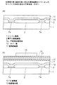
図1は、FeRAMのメモリセルの回路図の一例を示し、1ビットの情報の記憶に1つのトランジスタT0 と1つのキャパシタC0 を用いる1T1C型のメモリセルの回路図である。
【0004】
1T1C型メモリセルには、メモリセルから読み出された電荷が“1”のデータか又は“0”のデータかを判定するための基準電圧を発生させるリファレンスキャパシタC1 が必要となる。リファレンスキャパシタC1 は、データが読み出される毎にその分極が反転されることになる。データの判定は、各メモリセルのキャパシタC0 の電位とリファレンスキャパシタC1 の電位の大小関係に基づいて行われる。リファレンスキャパシタC1 は各ビット線BIT の端部に接続され、リファレンスキャパシタC1 の電位は理想的にはメモリセルに“1”を書き込む場合の電圧V1 と“0”を書き込む場合の電圧V0 の中間に設定するのが望ましい。
【0005】
メモリセルとしては、1T1C型の他に2T2C型がある。2T2C型のメモリセルは、1ビットの情報の記憶に2つのトランジスタと2つのキャパシタを用いる型式であり、一方のキャパシタに“1”又は“0”のデータを記憶し、他方のキャパシタに反対のデータを記憶するという相補的な動作をさせ、データの判定時には両方のキャパシタの分極状態を読み出して、その差分を用いてデータの判定を行う回路構成を有している。
【0006】
1T1C型式のメモリセルは、2T2C型式のメモリセルに比べてセル面積を約半分にすることが可能である。
【0007】
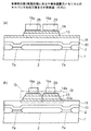
次に、1T1C型メモリセルの構造について説明する。図2は、1T1C型のメモリセルの平面図、図3は、そのI−I線断面図を示している。なお、図2では、半導体基板上の層間絶縁膜は省略されて描かれている。
【0008】
図2、図3において、半導体基板101 の表層には素子分離層102 に囲まれた活性領域(ウェル)103 が互いに間隔をおいて縦横に複数形成されている。各々の活性領域103 上には、Y方向に延びるワード線WLを兼ねた2つのゲート電極105 がゲート絶縁膜104 を介して形成されている。ワード線WLは、素子分離絶縁層102 の上に延在して形成されている。各活性領域103 においては、2つのゲート電極105 の両側の活性領域103 内に第1〜第3の不純物拡散領域107a,107b,107cが形成されている。
【0009】
一方のゲート電極105 とその両側の不純物拡散領域107a,107b は1つのMOSトランジスタT0 を構成し、さらに、他方のゲート電極105 とその両側の不純物拡散領域107b, 107cは別のMOSトランジスタT0 を構成している。即ち、各々の活性領域103 には2つのトランジスタT0 が形成されている。
【0010】
トランジスタT0 と素子分離絶縁層102 は絶縁性カバー膜108 により覆われ、また、絶縁性カバー膜108 上には第1層間絶縁膜109 が形成されている。
【0011】
第1層間絶縁膜109 の上であって素子分離絶縁層102 の上方には、Y方向に延在するストライプ状のキャパシタ下部電極111 がX方向に間隔をおいて複数形成され、そのキャパシタ下部電極111 の上には、これとほぼ同じ形状の強誘電体膜112 が形成され、さらに、強誘電体膜112 の上には複数のキャパシタ上部電極113 がY方向に一列に形成されている。1つのキャパシタ上部電極113 とその下の強誘電体膜112 及びキャパシタ下部電極111 によって1つのキャパシタC0 が構成される。
【0012】
また、キャパシタC0 と第1層間絶縁膜109 の上には第2の層間絶縁膜114 が形成されている。そして、第1及び第2層間絶縁膜109,114 、絶縁性カバー膜108 のうち活性領域103 内の第1〜第3の不純物拡散領域107a,107b,107cの上には、第1〜第3のコンタクトホール114a,114b,114cが形成されている。第1〜第3のコンタクトホール114a,114b,114c内には、それぞれ第1〜第3の導電性プラグ115a,115b,115cが形成されている。さらに、第2層間絶縁膜114 のうちキャパシタ上部電極113 の上には第4のコンタクトホール114dが形成され、その中には第4の導電性プラグ115dが形成されている。
【0013】
第2層間絶縁膜114 の上には、第1の導電性プラグ114aとこれに隣接する第4の導電性プラグ115dを接続するための第1の金属配線116aが形成されている。また、第2層間絶縁膜114 の上には、第3の導電性プラグ114cとこれに隣接する第4の導電性プラグ115dを接続するための第2の金属配線116cが形成されている。
【0014】
これにより、各キャパシタ下部電極111 の上方で一列に形成される複数のキャパシタ上部電極113 はそれぞれシリコン基板101 上のMOSトランジスタT0 に1対1で接続されることになる。
【0015】
なお、第2層間絶縁膜114 のうち第2の導電性プラグ115bの上には、金属パッド116bが形成される。その金属パッド116bには、その上方に第3層間絶縁膜(不図示)を介して形成されるビット線117 が接続される。ビット線117 は、ワード線WL、キャパシタ下部電極111 それぞれに交差する方向に延在している。
【0016】
【発明が解決しようとする課題】
ところで、上記したキャパシタは次のような方法によって形成される。
【0017】
第1の方法は、第1層間絶縁膜109 上に第1導電膜、強誘電体膜、第2導電膜を順に形成した後に、第2導電膜をパターニングしてキャパシタ上部電極113 を形成し、ついで、強誘電体膜と第1導電膜を同じマスクを用いてパターニングして強誘電体膜112 とキャパシタ下部電極111 を形成する方法である。
【0018】
第2の方法は、第1層間絶縁膜109 上に第1導電膜、強誘電体膜、第2導電膜を順に形成した後に、第2導電膜と強誘電体膜を同じマスクを用いてパターニングしてキャパシタ上部電極113 を形成し、ついで、第1導電膜をパターニングしてキャパシタ下部電極111 を形成する方法である。
【0019】
第3の方法は、第1層間絶縁膜109 上に第1導電膜、強誘電体膜、第2導電膜を順に形成した後に、第1導電膜、強誘電体膜、第2導電膜をそれぞれ別々のマスクを用いて個別にパターニングすることによりキャパシタ上部電極113 、強誘電体膜112 、キャパシタ下部電極111 を形成する方法である。
【0020】
第1、第2及び第3の方法によれば、キャパシタ上部電極113 を形成した後にキャパシタ下部電極111 を形成することになるので、キャパシタ下部電極111 のパターニングの際に使用されるマスクのズレによってキャパシタ上部電極113 の面積が縮小化されるおそれがある。キャパシタ上部電極113 の縮小化を防止するためにはキャパシタ下部電極111 を広く形成するようにすればよいが、これではメモリセル領域の高集積化の妨げになる。
【0021】
また、第2の方法によれば、キャパシタ下部電極111 上のキャパシタ上部電極113 同士の間の領域でキャパシタ下部電極111 が強誘電体膜112 から露出してしまうので、キャパシタ下部電極111 を構成するプラチナの触媒作用によってキャパシタの還元が促進されるおそれがある。
【0022】
さらに、第3の方法によれば、キャパシタ上部電極1113、強誘電体膜112 、キャパシタ下部電極111 が別々のマスクを使用して形成されるので、スループットが低下する。
【0023】
本発明の目的は、メモリセル領域に形成されるキャパシタ下部電極上の複数のキャパシタを精度良く形成することができる半導体装置及びその製造方法を提供することにある。
【0025】
【課題を解決するための手段】
上記した課題は、半導体基板の上方に第1絶縁膜を形成する工程と、前記第1絶縁膜の上に第1の導電膜、誘電体膜、第2の導電膜を順に形成する工程と、キャパシタ下部電極であるプレートラインのコンタクト領域を除いた形状を有する第1のマスクを使用して、前記第2の導電膜と前記誘電体膜をエッチングして第1パターン形状にする工程と、前記第1のマスクを除去する工程と、前記プレートラインのコンタクト領域から前記第2の導電膜の縁部にオーバーラップする第2パターンとキャパシタ形状の複数の第3パターンを有する第2のマスクを使用して、前記第1の導電膜と前記第1パターン形状の前記第2の導電膜を同時にエッチングすることにより、前記第2の導電膜からなる複数のキャパシタ上部電極を形成するとともに、前記第1パターン形状の前記誘電体膜に覆われ且つコンタクト領域を有するプレートラインを前記第1の導電膜から形成する工程と、前記第2のマスクを除去して、前記プレートラインの前記コンタクト領域と前記キャパシタ上部電極との間の領域に前記第2の導電膜から構成される孤立導電パターンを形成する工程とを有することを特徴とする半導体装置の製造方法によって達成する。
【0026】
本発明によれば、絶縁膜上に第1の導電膜、誘電体膜及び第2の導電膜を順に形成し、ついで第1のマスクを使用して第2の導電膜と誘電体膜を第1のパターン形状にパターニングした後に、第2のマスクを使用して第1の導電膜と第2の導電膜を同時にパターニングすることにより第2の導電膜から複数のキャパシタ上部電極を形成し、第1の導電膜からプレートライン(下部電極)を形成している。これにより、キャパシタ上部電極、誘電体膜及びキャパシタ下部電極によってキャパシタが構成されるとともに、プレートライン上ではキャパシタ上部電極の数だけキャパシタが存在する。
【0027】
従って、2つのマスクを用いることにより複数のキャパシタが形成されるので、キャパシタ形成工程のスループットが向上する。また、第1の導電膜と第2の導電膜を同時にパターニングしているので、エッチング条件を調整することにより誘電体膜を第1のパターンの状態で残すことが可能になり、プレートライン上の複数のキャパシタ上部電極の相互間の領域でプレートラインを誘電体膜で覆うことが可能になり、キャパシタ下部電極を構成する白金族金属の触媒によるキャパシタの還元が抑制されることになる。
【0028】
また、キャパシタ上部電極とキャパシタ下部電極を同時にパターニングしているので、キャパシタ上部電極の形成後のキャパシタ形成用のパターニングが無くなり、キャパシタ上部電極が再びエッチングされるおそれがなく、キャパシタ上部電極は精度良く形成されることになる。
【0029】
さらに、キャパシタ下部電極を形成するための第2のマスクとして、プレートラインのコンタクト領域を覆う第2パターンとキャパシタ形状の第3パターンを有するマスクを用いている。この場合、第2のマスクの位置ズレを考慮して、第2のマスクの第2パターンを第1の導電膜の縁にオーバーラップさせることになるが、これによりプレートラインのコンタクト領域の周辺で第2の導電膜からなる孤立導電パターンが形成されることになる。孤立導電パターンは層間絶縁膜により覆われるので、電気的に孤立して実動作セルを構成することはない。
【0030】
また、第2のマスクを使用して第1及び第2の導電膜をエッチングする際に、第2のマスクがエッチングガスと反応して縮小化するおそれがある。この対策として、第2の導電膜を第1のパターンの形状にパターニングした後であって第2のマスクを第2の導電膜上に形成する前に、第2の導電膜をキャパシタ保護絶縁膜によって覆い、その後に、第2のマスクによってキャパシタ保護膜をエッチングして第2のマスクの下に選択的に残すようにする。
【0031】
これによれば、キャパシタ上部電極形状のキャパシタ保護絶縁膜がマスクとして機能するので、第2のマスクが縮小化しても第2の導電膜は第2のマスクの初期の形状にパターニングされ、キャパシタ上部電極が精度良く形成される。
【0032】
【発明の実施の形態】
以下に本発明の実施形態を図面に基づいて説明する。
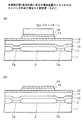
(第1の実施の形態)
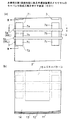
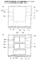
図4〜図8は、本発明の第1実施形態に係る半導体装置のメモリセルのキャパシタの形成工程を示す断面図である。図9〜図11は、本発明の第1実施形態に係る半導体装置のメモリセルのトランジスタ及びその周辺の形成工程を示す断面図である。図12〜図15は、本発明の第1実施形態に係る半導体装置のメモリセルのキャパシタの形成工程を示す平面図である。
【0033】
なお、図4〜図8は、図12のII−II線に沿った断面図であり、図9〜図11は、図12のIII-III 線に沿った断面図である。
【0034】
次に、図4(a) 、図9(a) 、図12(a) に示す構造を形成するまでの工程を説明する。
【0035】
まず、p型シリコン(半導体)基板1の表面に、LOCOS(Local Oxidation of Silicon)法によって素子分離絶縁膜2を形成する。なお、素子分離絶縁膜2として、LOCOS法によって形成されたシリコン酸化膜の他、STI(Shallow Trench Isolation)構造を採用してもよい。素子分離絶縁膜2は、シリコン基板1のメモリセル領域における所定の活性領域(トランジスタ形成領域)3を囲む範囲に形成される。
【0036】
活性領域3の平面形状は略長方形であり、帯状のプレートライン形成領域の両側に沿って間隔をおいて複数形成されている。
【0037】
その後、シリコン基板1の表面を熱酸化して、活性領域3の上でゲート絶縁膜4として使用されるシリコン酸化膜を形成する。
【0038】
次に、素子分離絶縁膜2及びゲート絶縁膜4の上にアモルファスシリコン膜とタングステンシリサイド膜を順に形成する。そして、アモルファスシリコン膜及びタングステンシリサイド膜をフォトリソグラフィ法により所定の形状にパターニングして、活性領域3の上にゲート電極5a,5bを形成する。メモリセル領域では、活性領域3上には2つのゲート電極5a,5bがほぼ平行に間隔をおいて形成され、これらのゲート電極5a,5bは素子分離絶縁膜2の上に延在してワード線WLとなる。ワード線WLは、プレートライン形成領域の延在方向に交差する方向に延在するように形成される。
【0039】
なお、ゲート電極5a,5bを構成するアモルファスシリコン膜の代わりにポリシリコン膜を形成してもよい。
【0040】
次に、活性領域3のうち、ゲート電極5a,5bの両側にn型不純物をイオン注入して、nチャネルMOSトランジスタT1 ,T2 のソース/ドレインとなる第1〜第3のn型不純物拡散領域7a,7b,7cを形成する。活性領域3の中央に位置する第2のn型不純物拡散領域7bはビット線に電気的に接続され、また、活性領域3の両側に位置する第1、第3のn型不純物拡散領域7a,7cはキャパシタに電気的に接続される。
【0041】
その後に、シリコン基板1、素子分離絶縁膜2及びゲート電極5a,5bの上に絶縁膜を形成する。そして、絶縁膜をエッチバックすることにより、ゲート電極5a〜5cの両側部分に側壁絶縁膜6として残す。その絶縁膜として、例えばCVD法により形成される酸化シリコン(SiO2)を使用する。
【0042】
さらに、活性領域3上のゲート電極5a,5b及び側壁絶縁膜6をマスクにして、n型不純物拡散領域7a〜7cにn型不純物をイオン注入することによりn型不純物拡散領域7a〜7cをLDD構造にする。
【0043】
これにより、第1及び第2のn型不純物拡散領域7a,7bとゲート電極5aを有する第1のnMOSトランジスタT1 の形成と、第2及び第3のn型不純物拡散領域7b,7cとゲート電極5bを有する第2のnMOSトランジスタT2 の形成が終了する。
【0044】
この後に、nMOSトランジスタT1 ,T2 を覆うカバー膜10をシリコン基板1上にプラズマCVD法により形成する。カバー膜10として例えば酸窒化シリコン(SiON)膜を形成する。
【0045】
次に、TEOSガスを用いるプラズマCVD法により、酸化シリコン(SiO2)膜を約1.0μmの厚さに成長し、この酸化シリコン膜を第1の層間絶縁膜11として使用する。
【0046】
続いて、第1の層間絶縁膜11の緻密化処理として、常圧の窒素雰囲気中で第1の層間絶縁膜11を700℃の温度で30分間熱処理する。その後に、第1の層間絶縁膜11の上面を化学機械研磨(CMP;Chemical Mechanical Polishing )法により研磨して平坦化する。
【0047】
なお、図12(a) では、素子分離絶縁膜2の上に形成される絶縁膜は省略されて描かれている。
【0048】
次に、図4(b) 、図9(b) 、図12(b) に示す構造を形成するまでの工程を説明する。
【0049】
まず、第1の層間絶縁膜11上に、第1の導電膜12としてTi膜とプラチナ(Pt)膜を順に形成する。Ti膜とPt膜はDCスパッタ法により形成される。この場合、Ti膜の厚さを10〜30nm程度、Pt膜の厚さを100〜300nm程度とする。なお、第1の導電膜12として、イリジウム、ルテニウム、酸化ルテニウム、酸化イリジウム、酸化ルテニウムストロンチウム(SrRuO3)等のいずれかの導電膜を形成してもよい。
【0050】
その後に、強誘電体膜13として厚さ100〜300nmのチタン酸ジルコン酸鉛(PZT; Pb(Zr1-xTix )O3 )膜をRFスパッタ法により第1の導電膜14上に形成する。強誘電体層13の形成方法は、その他に、MOD(metal organic deposition)法、MOCVD( 有機金属CVD)法、ゾル・ゲル法などがある。また、強誘電体層15の材料としては、PZT以外に、PLCSZT、PLZTのような他のPZT系材料や、SrBi2Ta2O9(SBT、Y1)、SrBi2(Ta,Nb)2O9 (SBTN、YZ)等のBi層状構造化合物、その他の金属酸化物強誘電体を採用してもよい。
【0051】
さらに、強誘電体膜13を構成するPZT膜の結晶化処理として、酸素雰囲気中で温度650〜850℃、30〜120秒間の条件でRTA(Rapid Thermal Annealing) を行う。例えば、温度700℃で60秒間アニールする。
【0052】
続いて、強誘電体膜13の上に第2の導電膜14として酸化イリジウム(IrO2)膜をスパッタ法により100〜300nmの厚さに形成する。なお、第2の導電膜14として、プラチナもしくは酸化ルテニウムストロンチウム(SRO)を用いてもよい。
【0053】
その後に、第2の導電膜14の上にレジストを塗布し、これを露光、現像することにより、プレートラインコンタクト領域を除いたプレートライン形成領域上に第1のレジストパターン15を形成する。
【0054】
次に、図5(a) 、図9(c) 、図13(a) に示すように、第1のレジストパターン15をマスクに使用して第2の導電膜14及び強誘電体膜13をエッチングする。これにより、第2の導電膜14と強誘電体膜13は、プレートラインコンタクト領域を除いたプレートライン形成領域とほぼ同じ形状になり、MOSトランジスタT1 、T2 の上から除去される。プレートライン形成領域の幅は約2.9μmである。
【0055】
この場合のエッチング条件は、例えば、誘導結合型プラズマエッチング装置を用い、塩素(Cl2)ガスを20ml/min. 、アルゴン(Ar)ガスを30ml/min. でエッチング雰囲気中に導入するとともに、エッチング雰囲気中の真空度を0.7Paとする。さらに、シリコン基板1が載置されるウェハステージ温度を25℃、ソースパワーを1400W、バイアスパワーを800Wに設定する。なお、ソースパワーは、誘導結合型プラズマエッチング装置のアンテナコイルに印加する13.56MHz の高周波電源のパワーである。また、バイアスパワーは、ウェハステージに印加する400KHz の高周波電源のパワーである。
【0056】
そのエッチングの際に、第1のレジストパターン15、第2の導電膜14及び強誘電体膜13の側面に導電性のエッチング生成物が付着すると、第1及び第2の導電膜12,14のパターニングにより形成されるキャパシタ上部電極とキャパシタ下部電極の間にリーク電流が流れ易くなる。このために、第1のレジストパターン15の側面を横方向に後退させるようなエッチング条件に設定することによって、第1のレジストパターン15の側面とエッチングされた膜の側面に付着する導電材を常に削りながらエッチングするようにすることが好ましい。この場合、第2のレジストパターン16a,16bの側面の後退を促進させる必要があり、その後退の調整は塩素とアルゴンのガス流量の調整によって行う。例えば塩素のガス比を高くし、アルゴンのガス比を低いする。
【0057】
続いて、図5(b) 、図13(b) に示すように、第1のレジストパターン15を除去する。
【0058】
次に、第1及び第2の導電膜12,14と強誘電体キャパシタ13の上にレジストを塗布する。続いて、図6(a) 、図14(a) に示すように、レジストを露光、現像することにより、プレートライン形成領域内に存在する第2の導電膜14の上に幅1.0μmで長さ1.7μmのキャパシタ上部電極形状の第2のレジストパターン16aを形成するとともに、プレートラインコンタクト領域から第2の導電膜14端部に僅かにオーバーラップする広さの第3のレジストパターン16bを形成する。このオーバーラップは、プレートラインコンタクト領域での位置合わせ時のズレ量を考慮した量とする。第2のレジストパターン16aは、プレートライン形成領域の長さ方向に沿って2列で複数個形成され、第2のレジストパターン16a同士の間隔を例えば0.3μmとする。
【0059】
この後に、図6(b) 、図14(b) に示すように、第2のレジストパターン16aに覆われない領域の第2の導電膜14をエッチングすると同時に、第3のレジストパターン16bと強誘電体膜13に覆われない領域の第1の導電膜12をエッチングする。
【0060】
これにより、第1の導電膜12はパターニングされてキャパシタの下部電極12aであるプレートラインとなる。また、第2の導電膜14はパターニングされて、各々のプレートライン12aの上方で2列に並ぶ複数の上部電極14aとなるとともに、帯状の強誘電体膜15のうちプレートラインコンタクト領域との境界部分に孤立導電パターン14bとして残される。また、図10(a) 、図15(a) に示すように、第1の導電膜12はMOSトランジスタT1 ,T2 の上方から除去される。
【0061】
この場合、第1及び第2の導電膜12,14のエッチング条件は、プレートライン領域内の強誘電体膜13が上部電極14aの周囲に残されるエッチング条件とする。また、上部電極14aとキャパシタ下部電極12aが同時に形成されるように、第1の導電膜12と第2の導電膜14のそれぞれの膜厚に応じたエッチング条件が設定されなければならない。さらに、上部電極14aと強誘電体膜13と下部電極12aの側壁に導電性物質を付着させないようなエッチング条件に設定して、上部電極14aと下部電極12aの間でリーク電流が流れないようにする必要がある。
【0062】
そのようなエッチング条件として、例えば、誘導結合型プラズマエッチング装置を用い、塩素(Cl2)ガスを20ml/min. 、アルゴン(Ar)ガスを30ml/min. でエッチング雰囲気中に導入するとともに、エッチング雰囲気中の真空度を0.7Paとする。さらに、シリコン基板1が載置されるウェハステージ温度を25℃、ソースパワーを1400W、バイアスパワーを800Wに設定する。
【0063】
このエッチングにより、第1の導電膜12と第2の導電膜14の一部を同時にエッチングすることにより、最終的なキャパシタQの上部電極14aと下部電極12aが同時に形成される。
【0064】
これにより、メモリセル領域では、下部電極12a、誘電体膜13及び上部電極14aを有するキャパシタQが形成される。即ち、プレートライン形成領域では、上部電極14aの数だけキャパシタQが形成されることになる。
【0065】
なお、孤立導電パターン14bの下にも、強誘電体膜13と下部電極12aが存在するが、孤立導電パターン14bは、電気的に孤立された状態に置かれるので、キャパシタとして動作することはない。
【0066】
その後に、図7(a) 、図15(a) に示すように、第2、第3のレジストパターン16a,16bを除去する。
【0067】
次に、図7(b) 、図10(b) に示すように、キャパシタQと第1の層間絶縁膜11の上にキャパシタ保護絶縁膜17として例えばアルミナを20nm程度の厚さに形成する。なお、キャパシタ保護絶縁膜17としては、アルミナの他、PZT、窒化シリコン膜、又は窒化酸化シリコン膜などを適用してもよい。
【0068】
さらに、キャパシタ保護絶縁膜17の上に第2の層間絶縁膜18として酸化シリコン膜を約1μmの厚さに形成する。この酸化シリコン膜は、TEOS、ヘリウム及び酸素の混合ガスを用いて、CVD法により形成される。
【0069】
続いて、第2の層間層間絶縁膜18の上面をCMP法により平坦化する。この例では、CMP後の第2層間絶縁膜18の残り膜厚は、メモリセル領域AのキャパシタQの上でキャパシタ保護絶縁膜17の膜厚と合わせて約300nm程度とする。
【0070】
次に、図8(a) 、図11(a) に示す構造を形成するまでの工程を説明する。
【0071】
まず、第2の層間絶縁膜18、キャパシタ保護絶縁膜17、第1層間絶縁膜11及びカバー膜10をフォトリソグラフィー法によりパターニングすることにより、第1、第3のn型不純物拡散領域7a,7cの上にそれぞれキャパシタコンタクトホール18aを形成すると同時に、第2のn型不純物拡散領域7bの上にビット線コンタクトホール18bを形成する。
【0072】
その後、第2の層間絶縁膜18上とキャパシタコンタクトホール18a内とビット線コンタクトホール18b内に、膜厚20nmのTi膜と膜厚50nmのTiN 膜をスパッタにより順に形成し、さらにTiN 膜の上にW膜をCVD方により形成する。W膜は、キャパシタコンタクトホール18aとビット線コンタクトホール18b内を完全に埋め込む厚さに形成される。
【0073】
続いて、Ti膜、TiN 膜及びW膜をCMP法により研磨して第2の層間絶縁膜18の上面上から除去する。これにより、キャパシタコンタクトホール18a内に残されたTi膜、TiN 膜及びW膜をキャパシタコンタクト用の第1の導電性プラグ19aとして使用し、また、ビット線コンタクトホール18b内に残されたTi膜、TiN 膜及びW膜をビット線コンタクト用の第2の導電性プラグ19bとして使用する。
【0074】
次に、図8(b) 、図11(b) 、図15(b) に示す構造を形成するまでの工程を説明する。
【0075】
まず、第2の層間絶縁膜18の上と第1、第2の導電性プラグ19a,19bの上に、アルミナなどからなる酸化防止絶縁膜(不図示)を形成する。続いて、酸化防止絶縁膜、第2層間絶縁膜18及びキャパシタ保護絶縁膜17をパターニングすることにより、上部電極16aの上にキャパシタコンタクト用のホール18c形成する。これと同時に、第2層間絶縁膜18及びキャパシタ保護絶縁膜17をパターニングして、プレートライン12aのプレートラインコンタクト領域の上にプレートラインコンタクト用のホール18dを形成する。
【0076】
その後に、酸化防止絶縁膜をエッチバックにより除去する。さらに、第2の層間絶縁膜18上と第1、第2の導電性プラグ19a,19b上とホール18c,18d内に、配線用金属膜として膜厚150nmのTiN 膜、膜厚5nmのTi膜、膜厚500nmのAl-Cu 膜、膜厚50nmのTiN 膜及び膜厚20nmのTi膜からなる5層構造の金属膜を形成した後に、配線用金属膜をフォトリソグラフィー法によりパターニングする。
【0077】
この配線用金属膜のパターニングにより、上部電極16aのホール18c内とその側方の第1の導電性プラグ19aを電気的に接続する第1の配線20aを形成するとともに、プレートラインコンタクト領域の上のホール18dを通してプレートライン12aに接続される第2の配線20dを形成する。これと同時に、第2の導電性プラグ19bの上に導電性パッド20bを形成する。
【0078】
これにより、プレートライン12a上の2列のキャパシタQの上部電極14aと第1又は第3のn型不純物拡散領域7a,7cは、第1の配線20aと第1の導電性プラグ19aを介して電気的に接続される。
【0079】
なお、第2のn型不純物拡散領域7bは、上方に形成されるビット線(不図示)に導電性パッド20b及び第2の導電性プラグ19bを介して電気的に接続される。
【0080】
配線20a,20dと導電性パッド20bを形成した後に、その上に第3の層間絶縁膜を形成し、導電性プラグを形成し、さらに第3の層間絶縁膜の上にビット線などを形成するが、その詳細は省略する。
【0081】
以上の実施形態においては、キャパシタQの下部電極であるプレートライン12aを覆う強誘電体膜13の上に複数の上部電極14aをプレートライン12aの延在方向に二列に複数個形成している。従って、一例に複数個搭載されるプレートライン(下部電極)を用いる従来技術とは異なり、プレートライン12aの両側にMOSトランジスタT1 ,T2 を形成することになるので、プレーライン相互間の無駄なスペースが従来よりも少なくなり、メモリセル領域を従来よりもさらに高集積化することが可能になる。
【0082】
また、第1の導電膜12、強誘電体膜13、第2の導電膜14をパターニングしてキャパシタQを形成する工程は、第1の導電膜12と強誘電体膜13を同一マスクを用いてパターニングしてプレートライン形成領域に残した後に、第2の導電膜14と第1の導電膜12を同時にパターニングして2列の上部電極14aとプレートライン(下部電極)12aを同時に形成している。
【0083】
従って、2回のパターニング工程によってキャパシタQを形成することができるので、スループットが良好である。しかも、プレートライン12aを構成するプラチナが上部電極14a相互間の領域で露出することはなく、プラチナの触媒による還元作用をキャパシタQに及ぼすことが防止される。
【0084】
ところで、図5(b) に示した第2の導電膜14のパターンを第1のパターンとし、図6(b) に示した上部電極14aを第2のパターンとする。そして、第1のパターンに対して第2のパターンに位置ずれが生じた場合に、左右の第2のパターンの大きさを一定とする条件は以下の式(1)で表される。なお、式(1)においてWTE-1stは第1のパターンの幅、WTE-FINALは第2のパターン(上部電極)の幅、WALLIGNは位置ズレ最大量、WTE-GAPはプレートライン形成領域における2列の第2のパターン(上部電極)同士の間隔を示している。
【0085】
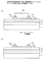
WTE-1st > 2×(WTE-FINAL + WALLIGN)+ WTE-GAP (1) (第2の実施の形態)
本実施形態では、キャパシタ製造工程においてプレートラインのコンタクト領域の露出面積を狭くする方法について説明する。
【0086】
図16〜図19は、本発明の第2実施形態に係る半導体装置のメモリセルのキャパシタ形成工程を示す断面図である。図20〜図23は、本発明の第2実施形態に係る半導体装置のメモリセルのキャパシタ形成工程を示す断面図である。なお、図20〜図23は、図16のIV−IV線から見た断面図である。
【0087】
まず、第1実施形態に係る図4(a) 、図9(a) 、図12(a) に示したように、シリコン基板1に素子分離絶縁膜2、MOSトランジスタT1 ,T2 、カバー膜10、第1層間絶縁膜11などを形成する。
【0088】
次に、図16(a) 、図20(a) に示すように、第1層間絶縁膜11上に、第1の導電膜12、強誘電体膜13、第2の導電膜14を順に形成する。第1の導電膜12、強誘電体膜13、第2の導電膜14は、それぞれ第1実施形態に示した材料により構成される。なお、強誘電体膜13は、成膜後に結晶化のためのアニールがなされる。
【0089】
その後に、第2の導電膜14の上にレジストを塗布し、これを露光、現像することにより、プレートライン(下部電極)形状の第1のレジストパターン21を形成する。第1のレジストパターン21は、プレートラインコンタクト部分に開口21aを有している。
【0090】
なお、図20〜図23は、プレートラインのコンタクト領域及びその周辺を示している。
【0091】
次に、図16(b) 、図20(b) に示すように、第1のレジストパターン21をマスクに使用して第2の導電膜14及び強誘電体膜13をエッチングする。これにより、第2の導電膜14と強誘電体膜13は、プレートラインとほぼ同じ平面形状になり、プレートラインコンタクト領域から第1の導電膜12を露出する開口13aを有することになる。プレートラインの幅は例えば2.9μm程度である。なお、第2の導電膜14と強誘電体膜13は、MOSトランジスタT1 、T2 の上から除去される。
【0092】
この場合のエッチング条件は、例えば、誘導結合型プラズマエッチング装置を用い、塩素(Cl2)ガスを20ml/min. 、アルゴン(Ar)ガスを30ml/min. でエッチング雰囲気中に導入するとともに、エッチング雰囲気中の真空度を0.7Paとする。さらに、シリコン基板1が載置されるウェハステージ温度を25℃、ソースパワーを1400W、バイアスパワーを800Wに設定する。
【0093】
そのエッチングの際に、第1のレジストパターン21及びエッチングされた第2の導電膜14及び強誘電体膜13の側面に導電性物質が付着すると、この後に第1及び第2の導電膜12,14のパターニングにより形成されるキャパシタ上部電極とキャパシタ下部電極の間にリーク電流が流れ易くなる。このために、第2のレジストパターンを横方向に後退させるようなエッチング条件に設定することにより、それらの側面に付着する導電材を削りながら第2の導電膜14及び強誘電体膜13をエッチングすることが好ましい。この場合、第2のレジストパターン16a,16bの側面の後退を促進する必要があり、その後退の調整として例えば塩素のガス比を高く、アルゴンのガス比を低くする。
【0094】
続いて、図17(a) 、図21(a) に示すように、第1のレジストパターン21を除去する。
【0095】
次に、第1及び第2の導電膜12,14と強誘電体膜13の上にレジストを塗布する。続いて、図17(b) 、図21(b) に示すように、レジストを露光、現像することにより、プレートライン形成領域内の第2の導電膜14の上に幅1.0μmで長さ1.7μmのキャパシタ上部電極形状の第2のレジストパターン22aを形成するとともに、プレートラインコンタクト領域及びその周辺に第3のレジストパターン22bを形成する。第2のレジストパターン22aは、プレートライン形成領域の長さ方向に沿って2列で複数個形成され、また、第2のレジストパターン16a同士の間隔を約0.3μmとする。
【0096】
この後に、図18(a) 、図22(a) に示すように、第2のレジストパターン22aに覆われない領域の第2の導電膜14をエッチングすると同時に、第3のレジストパターン22bと強誘電体膜13に覆われない領域の第1の導電膜12をエッチングする。その後に、図18(b) 、図22(b) に示すように、第2、第3のレジストパターン22a,22bを除去する。
【0097】
これにより、第1の導電膜12はパターニングされてキャパシタ下部電極であるプレートライン12bとなる。また、第2の導電膜14はパターニングされてプレートライン12bの上方において2列で平行に並ぶ複数の上部電極14aとなるとともに、プレートラインコンタクト領域の周辺を囲む枠状の孤立導電パターン14cとして残される。なお、第1実施形態と同様に、第1の導電膜12はMOSトランジスタT1 ,T2 の上方から除去される。
【0098】
このエッチングで、第1の導電膜12と第2の導電膜14の一部を同時にエッチングすることにより、最終的なキャパシタQの上部電極14aと下部電極(プレートライン)b同時に形成される。
【0099】
この場合、第1及び第2の導電膜12,14のエッチング条件は、プレートライン12bで強誘電体膜13が上部電極14a相互間領域とプレートラインコンタクト領域の周辺に残されるエッチング条件とする。また、上部電極14aと下部電極12bが同時に形成されるように、第1の導電膜12と第2の導電膜14のそれぞれの膜厚に応じたエッチング条件が設定されなければならない。さらに、上部電極14aと強誘電体膜13と下部電極b側壁に導電性物質を付着させないようになエッチング条件にして、上部電極14aと下部電極12bの間でリーク電流が流れないようにする必要がある。
【0100】
そのようなエッチング条件として、例えば、誘導結合型プラズマエッチング装置を用い、塩素(Cl2)ガスを20ml/min. 、アルゴン(Ar)ガスを30ml/min. でエッチング雰囲気中に導入するとともに、エッチング雰囲気中の真空度を0.7Paとする。さらに、シリコン基板1が載置されるウェハステージ温度を25℃、ソースパワーを1400W、バイアスパワーを800Wに設定する。
【0101】
以上により、メモリセル領域では、下部電極12b、誘電体膜13及び上部電極14aからなるキャパシタQが形成される。即ち、プレートライン形成領域では、上部電極14aの数だけキャパシタQが形成されることになる。
【0102】
なお、プレートラインコンタクト領域の周囲に存在する孤立導電パターン14cの下にも強誘電体膜13と下部電極12bが存在するが、孤立導電パターン14cは、電気的に孤立された状態に置かれるので、キャパシタの上部電極として機能しない。
【0103】
この後に、第1実施形態に係る図7(b) 、図10(b) に示したと同様に、キャパシタQと第1の層間絶縁膜11の上にキャパシタ保護絶縁膜17を200nm程度の厚さに形成する。さらに、キャパシタ保護絶縁膜17の上に第2の層間絶縁膜18を約1μmの厚さに形成する。続いて、第2の層間層間絶縁膜18の上面をCMP法により平坦化する。
【0104】
次に、図19、図23に示す構造を形成するまでの工程を説明する。
【0105】
まず、第2の層間絶縁膜18、キャパシタ保護絶縁膜17、第1層間絶縁膜11及びカバー膜10をフォトリソグラフィー法によりパターニングすることにより、第1、第3のn型不純物拡散領域7a,7cの上にそれぞれキャパシタコンタクトホール18aを形成すると同時に、第2のn型不純物拡散領域7bの上にビット線コンタクトホール18bを形成する。
【0106】
その後、第1実施形態と同様な工程により、第2の層間絶縁膜18上とキャパシタコンタクトホール18a内とビット線コンタクトホール18b内に、それぞれTi膜とTiN 膜とW膜から構成される第1の導電性プラグ19aと第2の導電性プラグ19bを形成する。
【0107】
続いて、第1実施形態と同様な工程により、第2層間絶縁膜18及びキャパシタ保護絶縁膜17をパターニングすることにより、上部電極16aの上にキャパシタコンタクト用のホール18cを形成するとともに、プレートライン12b上の強誘電体膜13の開口部13a上にプレートラインコンタクト用のホール18dを形成する。
【0108】
その後に、第2の層間絶縁膜18上と第1、第2の導電性プラグ19a,19b上とホール18c,18d内に、配線用金属膜を形成した後に、配線用金属膜をフォトリソグラフィー法によりパターニングする。
【0109】
この配線用金属膜のパターニングにより、キャパシタコンタクト用のホール18c内とその側方の第1の導電性プラグ19aを電気的に接続する第1の配線20aを形成する。これと同時に、第2の導電性プラグ19bの上に導電性パッド20bを形成するとともに、プレートラインコンタクト用のホール18d内から引出される第2の配線20cを形成する。
【0110】
これにより、プレートライン12b上で2列に形成された複数のキャパシタQの上部電極14aは、第1の配線20aを介して第1又は第3のn型不純物拡散領域7a、7cに電気的に接続される。
【0111】
また、第2の配線20cは、プレートライン12bに接続されて周辺回路領域(不図示)のプレートライン制御回路に接続される。
【0112】
なお、第2のn型不純物拡散領域7bは、その上方に形成されるビット線(不図示)に導電性パッド20b及び第2の導電性プラグ19bを介して電気的に接続される。
【0113】
配線20a,20dと導電性パッド20bを形成した後に、その上に第3の層間絶縁膜を形成し、導電性プラグを形成し、さらに第3の層間絶縁膜の上にビット線などを形成するが、その詳細は省略する。
【0114】
以上の実施形態においては、キャパシタQの下部電極であるプレートライン12bを覆う強誘電体膜13の上に複数の上部電極14aをプレートライン12bの延在方向に二列に複数個形成しているので、第1実施形態と同様に、メモリセル領域を従来よりもさらに高集積化することが可能になる。
【0115】
また、第1の導電膜12、強誘電体膜13、第2の導電膜14をパターニングしてキャパシタQを形成する工程は、第1の導電膜12と強誘電体膜13をプレートラインとほぼ同じ平面形状に同時にパターニングした後に、第2の導電膜14と第1の導電膜12を同時にパターニングして下部電極12bとその上の2列の上部電極14aを同時に形成している。従って、2回のパターニングによってキャパシタQを形成でき、キャパシタ形成工程を短くできる。しかも、下部電極12bを構成するプラチナが上部電極14a相互間領域に露出することはなく、プラチナの触媒作用による還元をキャパシタQに及ぼすことが抑制される。
【0116】
さらに、プレートライン12bのプレートラインコンタクト部の周辺も強誘電体膜13に覆われた状態となるので、第1実施形態に比べてさらにプレートライン12bによる触媒作用を抑制することができる。
(第3の実施の形態)
本実施形態では、半導体装置におけるキャパシタの上部電極をさらに高精度に形成するキャパシタの製造工程についてい説明する。
【0117】
図24〜図26は、本発明の第3実施形態に係る半導体装置のメモリセルのキャパシタ形成工程を示す断面図である。図27〜図29は、本発明の第2実施形態に係る半導体装置のメモリセルのキャパシタ形成工程を示す断面図である。なお、図24〜図26は、図27のV−V線から見た断面図である。
【0118】
まず、第1実施形態に係る図4(a) 、図9(a) 、図12(a) に示したように、シリコン基板1に素子分離絶縁膜2、MOSトランジスタT1 ,T2 、カバー膜10、第1層間絶縁膜11などを形成する。さらに、図4(b) 、図12(b) に示したように、第1層間絶縁膜11上に、第1の導電膜12、強誘電体膜13、第2の導電膜14を順に形成し、その後に第1のレジストパターン15を用いて第2の導電膜14及び強誘電体膜13をエッチングする。これにより、図5(b) 、図13(b) に示したように、プレートライン形成領域のうちプレートラインコンタクト領域を除いた形状に強誘電体膜13、第2の導電膜14をパターニングする。そのエッチングは、第1実施形態に示した条件に従う。
【0119】
その後に、図24(a) 、図27(a) に示すように、パターニングされた第2の導電膜14、強誘電体膜13及び第1の導電膜12の上に第1のキャパシタ保護絶縁膜25として厚さ50nmのアルミナ膜をスパッタにより形成する。第1のキャパシタ保護絶縁膜25として、エッチング選択性とキャパシタ保護性を兼ね備えた材料からなる膜が好ましく、アルミナ膜の他に酸化チタン膜などを形成してもよい。
【0120】
次に、第1のキャパシタ保護絶縁膜25の上にレジストを塗布する。続いて、図24(b) 、図27(b) に示すように、レジストを露光、現像することにより、プレートライン形成領域内に存在する第2の導電膜14の上方に幅1.0μmで長さ1.7μmのキャパシタ上部電極形状の第2のレジストパターン16aを形成するとともに、プレートラインコンタクト領域から第2の導電膜14端部に僅かにオーバーラップする大きさの第3のレジストパターン16bを第1のキャパシタ保護絶縁膜25上に形成する。このオーバーラップは、プレートラインコンタクト領域での位置合わせ時のズレ量を考慮した量とする。
【0121】
複数の第2のレジストパターン16aは、プレートライン形成領域の長さ方向に沿って2列で複数個形成され、第2のレジストパターン16a同士の間隔を0.3μmとする。
【0122】
次に、図25(a) 、図28(a) に示すように、第2及び第3のレジストパターン16a,16bをマスクに使用して第1のキャパシタ保護絶縁膜25をエッチングする。この場合に、第1のキャパシタ保護絶縁膜25のエッチングは、第2及び第3のレジストパターン16a,16bの側面の後退の少ない条件で行われる。
【0123】
例えば、誘導結合型プラズマエッチング装置を用い、塩素(Cl2)ガスを5ml/min. 、アルゴン(Ar)ガスを45ml/min. でエッチング雰囲気中に導入するとともに、エッチング雰囲気中の真空度を0.7Paとする。さらに、シリコン基板1が載置されるウェハステージ温度を25℃、ソースパワーを1400W、バイアスパワーを800Wに設定する。レジストパターン16a,16bの後退速度は塩素ガス比を変えることで調整することができる。
【0124】
レジストは、塩素との反応により揮発するため、この条件のように塩素ガス比が少なくてアルゴンガス比が高い条件を用いることによりレジストパターン16a,16bの後退を抑制できる。これにより、第1のキャパシタ保護絶縁膜25は、初期の第2、第3のレジストパターン16a,16bにほぼ近い平面形状にパターニングされる。
【0125】
そのようなエッチング条件によれば、第1及び第2の導電膜12,14のエッチングも可能である。しかし、エッチングにより生じる導電性の生成物がレジストパターン16a,16bの側面と第1及び第2の導電膜12,14のエッチング側面、及び強誘電体膜13の側面に付着して、キャパシタのリーク電流を増大させる原因になる。
【0126】
そこで、第1のキャパシタ保護絶縁膜25のエッチングを終えた後に、第2及び第3のレジストパターン16a,16bの側面が後退するようなエッチング条件に変える。
【0127】
そのエッチング条件として、例えば、誘導結合型プラズマエッチング装置を用い、塩素(Cl2)ガスを15ml/min. 、アルゴン(Ar)ガスを35ml/min. でエッチング雰囲気中に導入するとともに、エッチング雰囲気中の真空度を0.7Paとする。さらに、シリコン基板1が載置されるウェハステージ温度を25℃、ソースパワーを1400W、バイアスパワーを800Wに設定する。
【0128】
このように塩素ガス比を上げることにより、レジストパターン16a,16bを適度に後退させ、第1及び第2の導電膜12,14のエッチングにより生じる反応生成物を側壁に付着することが防止される。
【0129】
なお、第1及び第2の導電膜12,14をエッチングする際に、第2及び第3のレジストパターン16a,16bだけでなく第1のキャパシタ保護絶縁膜25がマスクとなる。
【0130】
このエッチングにより、図25(b) 、図28(b) に示すように、第2、第3のレジストパターン16a,16bが初期状態よりも縮小されるとともに、第1の導電膜12と第2の導電膜14の一部が同時にエッチングされて、最終的なキャパシタQの上部電極14aと下部電極12aが同時に形成される。
【0131】
この後に、第2、第3のレジストパターン16a,16bを除去する。
【0132】
これにより、第1の導電膜12はパターニングされてキャパシタ下部電極12aであるプレートラインとなる。また、第2の導電膜14はパターニングされて2列で平行に並ぶ複数の上部電極14aとなるとともに、プレートラインコンタクト領域と強誘電体膜13との境界部分に孤立導電パターン14bとして残される。
【0133】
これにより、メモリセル領域では、下部電極12a、誘電体膜13及び上部電極14aを有するキャパシタQが形成される。即ち、プレートライン形成領域では、上部電極14aの数だけキャパシタQが形成されることになる。
【0134】
なお、孤立導電パターン14bの下にも、強誘電体膜13と下部電極12aが存在するが、孤立導電パターン14bは、電気的に孤立された状態に置かれるので、キャパシタの上部電極として動作することはない。
【0135】
次に、図26(a) に示すように、キャパシタQ、第1の保護膜25及び第1の層間絶縁膜11の上に第2のキャパシタ保護絶縁膜17として例えばアルミナを200nm程度の厚さに形成する。なお、キャパシタ保護絶縁膜17としては、アルミナの他、PZT、窒化シリコン膜、又は窒化酸化シリコン膜などを適用してもよい。
【0136】
さらに、キャパシタ保護絶縁膜17の上に第2の層間絶縁膜18として酸化シリコン膜を約1μmの厚さに形成する。続いて、第2の層間層間絶縁膜18の上面をCMP法により平坦化する。
【0137】
次に、図26(b) 、図29に示す構造を形成するまでの工程を説明する。
【0138】
まず、第2の層間絶縁膜18、第2のキャパシタ保護絶縁膜17、第1層間絶縁膜11及びカバー膜10をフォトリソグラフィー法によりパターニングすることにより、第1、第3のn型不純物拡散領域7a,7cの上にそれぞれキャパシタコンタクトホール18aを形成すると同時に、第2のn型不純物拡散領域7bの上にビット線コンタクトホール18bを形成する。
【0139】
その後、第1実施形態と同じ工程によって、キャパシタコンタクトホール18a内にキャパシタコンタクト用の第1の導電性プラグ19aを形成し、ビット線コンタクトホール18b内にビット線コンタクト用の第2の導電性プラグ19bを形成する。
【0140】
次に、第2層間絶縁膜18及び第1及び第2のキャパシタ保護絶縁膜17,25をパターニングすることにより、上部電極16aの上にキャパシタコンタクト用のホール18cを形成する。同時に、第2層間絶縁膜18及び第2のキャパシタ保護絶縁膜17をパターニングすることにより、プレートライン12aのプレートラインコンタクト領域の上にプレートラインコンタクト用のホール18dを形成する。
【0141】
その後に、第2の層間絶縁膜18上と第1、第2の導電性プラグ19a,19b上とホール18c,18d内に、配線用金属膜を形成した後に、配線用金属膜をフォトリソグラフィー法によりパターニングする。
【0142】
この配線用金属膜のパターニングにより、ホール18c内とその側方の第1の導電性プラグ19aを電気的に接続する第1の配線20aを形成する。これと同時に、第2の導電性プラグ19bの上に導電性パッド20bを形成する。さらに、プレートラインコンタクト領域のホール18d内と第2の層間絶縁膜18上に第2の配線20dを形成する。
【0143】
これにより、プレートライン12a上で2列に形成された上部電極14aと第1又は第3のn型不純物拡散領域7aが、配線20aと第1の導電性プラグ19aを介して電気的に接続される。
【0144】
なお、第2のn型不純物拡散領域7bは、上方に形成されるビット線(不図示)に導電性パッド20b及び第2の導電性プラグ19bを介して電気的に接続される。
【0145】
配線20a,20dと導電性パッド20bを形成した後に、その上に第3の層間絶縁膜を形成し、導電性プラグを形成し、さらに第3の層間絶縁膜の上にビット線などを形成するが、その詳細は省略する。
【0146】
以上の実施形態においては、キャパシタ下部電極であるプレートライン12bを覆う強誘電体膜13の上に複数の上部電極14aをプレートライン12aの延在方向に二列に複数個形成しているので、第1実施形態と同様に、メモリセル領域を従来よりもさらに高集積化することが可能になる。
【0147】
また、第1の導電膜12、強誘電体膜13、第2の導電膜14をパターニングしてキャパシタQを形成する工程は、第1の導電膜12と強誘電体膜13をプレートラインに沿った平面形状に同時にパターニングした後に、第2の導電膜14と第1の導電膜12を同時にパターニングして下部電極12aとその上の2列の上部電極14aとを同時に形成している。
【0148】
従って、キャパシタ形成工程が2枚のレジストマスクで形成することができ、スループットが向上するだけでなく、下部電極12bを構成するプラチナが上部電極14a相互間領域で露出することはなく、プラチナの触媒による還元作用をキャパシタQに及ぼすことが抑制される。
【0149】
さらに、キャパシタ上部電極形状にパターニングされた第1のキャパシタ保護絶縁膜25によって第2の導電膜14を覆った状態で、レジストパターン16aを後退する条件で第2の導電膜14をエッチングしている。これにより、レジストパターン16aの側面が後退することにより、上部電極14a、強誘電体膜13及び下部電極12aの側面には付着する反応生成物はエッチングによって除去され、しかも、第1のキャパシタ保護絶縁膜25をマスクとして機能させることによって上部電極14aのパターン精度を高めることができる。
【0150】
また、プレートライン12bの上面が、プレートラインコンタクト部の周辺でも第1のキャパシタ保護絶縁膜25に覆われた状態となるので、第1実施形態に比べてさらにプラチナの触媒作用を抑制することができる。
(比較例)
ところで、1つのプレートラインの上に複数のキャパシタ上部電極を2列に形成する工程としては以下の3つの例が考えられるが、上記した第1〜第3実施形態に比べてパターニング工程が増えたり、又はプレートラインの触媒作用を防止することが難しい。
【0151】
比較例1
図30は、比較例1に係るキャパシタの形成工程を示す平面図である。図31は、比較例1に係るキャパシタの形成工程を示す断面図であって、図30(a) に示すVI−VI線から見た断面図である。
【0152】
まず、図30(a) 、図31(a) に示すように、層間絶縁膜51の上に第1の導電膜52、強誘電体膜53、第2の導電膜54を順に形成した後に、第1のレジストパターン(不図示)を用いて第2の導電膜54をパターニングして複数の上部電極54aをプレートライン形成領域に沿って2列に形成する。その後に、上部電極54a及び強誘電体膜53の上にレジストを塗布し、これを露光、現像してセルプレートライン形成領域のうちセルプレートコンタクト領域を除く部分に第2のレジストパターン55を形成する。この場合、プレートライン形成領域の両側に位置する上部電極54aの側面と第2のレジストパターン55の両側面とをほぼ一致させる。
【0153】
次に、図30(b) 、図31(b) に示すように、第2のレジストパターン55をマスクに使用して強誘電体膜53をエッチングした後に、第2のレジストパターン55を除去する。
【0154】
さらに、図30(c) 、図31(c) に示すように、上部電極54a、強誘電体膜53及び第1の導電膜52の上にレジストを塗布し、これを露光、現像してセルプレートライン形成領域を覆う第3のレジストパターン56を形成する。
【0155】
続いて、図30(d) 、図31(d) に示すように、第3のレジストパターン56をマスクに使用して第1の導電膜52をエッチングすることにより、下部電極56aを形成する。その後に、第3のレジストパターン56を除去する。
【0156】
以上のようなキャパシタの形成工程によれば、第1の導電膜52,強誘電体膜53、第2の導電膜54をそれぞれ別々にパターニングするためのレジストパターンを3回形成する必要がある。
【0157】
これに対して、上記した実施形態では、強誘電体膜13と第2の導電膜14を同時にパターニングし、さらに第2の導電膜14と第1の導電膜12を同時にパターニングしているので、レジストパターンの形成は2回と少なくなる。
【0158】
また、比較例1では、強誘電体膜53のパターニング用の第2のレジストパターン55と、第1の導電膜52のパターニング用の第3のレジストパターン56のそれぞれの形成位置にずれが生じると、強誘電体膜53のエッチング又は第1の導電膜52のエッチングの際に、左又は右の上部電極52aがエッチングされて左右の上部電極52aの面積にバラツキが生じるおそれがある。上部電極52aのバラツキは、メモリセル領域内の複数のキャパシタの容量が不均一になる原因となる。しかも、上部電極52aを形成した後に、上部電極52aは2回のエッチング雰囲気に曝されるおそれがある。
【0159】
上部電極54aの面積のバラツキは、キャパシタ電荷のバラツキの原因となって、デバイス動作マージンに影響を与える。特に、1T1C型FeRAMでは、リファレンスキャパシタとメモリセルのキャパシタとを比較することにより、「1」と「0」の読み出しを行うために、個々のキャパシタ電荷量のバラツキは深刻な問題となる。
【0160】
これに対して、上記した実施形態では、上部電極14aの形成は、下部電極12aの形成と同時であり、その後に、キャパシタ形成工程で上部電極14aがエッチングに曝されることはない。しかも、第1実施形態で示した式(1)に従ってマージンを予め確保することにより、複数のキャパシタ上部電極14aの面積はほぼ均一になる。
【0161】
比較例2
図32は、比較例2に係るキャパシタの形成工程を示す平面図である。図331は、比較例2に係るキャパシタの形成工程を示す断面図であって、図32(a) に示すVII −VII 線から見た断面図である。
【0162】
比較例2は、図32(a) 〜(d) 、図33(a) 〜(d) に示すように、比較例1とほぼ同じ工程によってプレートライン上に複数のキャパシタを2列で形成する工程を示している。
【0163】
比較例2では、上部電極54aのパターンに対して第2のレジストパターン55や第3のレジストパターン56の位置ズレを予め想定して、その位置ズレ分だけ上部電極54aの幅を縮小させている点で比較例1とは異なっている。
【0164】
これにより、比較例2によれば、第2のレジストパターン55及び第3のレジストパターン56の両側面を上部電極54aの側面よりも外側に位置するように形成できることになり、上部電極54aのパターンは均一に形成できる。
【0165】
しかし、上部電極54aの面積が小さくなるのでセル面積効率が悪化するし、3枚のレジストパターンを用いなければならずスループットが低下する。
【0166】
比較例3
図34は、比較例3に係るキャパシタの形成工程を示す平面図である。図35は、比較例3に係るキャパシタの形成工程を示す断面図であって、図34(a) に示すVIII−VIII線から見た断面図である。
【0167】
まず、図34(a) 、図35(a) に示すように、層間絶縁膜61の上に第1の導電膜62、強誘電体膜63、第2の導電膜64を順に形成する。
【0168】
次に、図34(b) 、図35(b) に示すように、キャパシタ形状の第1のレジストパターン65を用いて第2の導電膜64及び強誘電体膜63をパターニングして複数のキャパシタ上部電極64aとキャパシタ誘電体膜63aをプレートライン形成領域に沿って2列に形成する。続いて、第1のレジストパターン65を除去する。
【0169】
次に、図34(c) 、図35(c) に示すように、上部電極64a、強誘電体膜63及び第1の導電膜62の上にレジストを塗布し、これを露光、現像してセルプレートライン形状の第2のレジストパターン66を形成する。この場合、プレートライン形成領域内の左右に存在する上部電極64aの側面と第2のレジストパターン65の両側面とをほぼ一致させるように、第2のレジストパターン66を形成する。
【0170】
次に、図34(d) 、図35(d) に示すように、第2のレジストパターン66をマスクに使用して第1の導電膜62をエッチングした後に、第2のレジストパターン66を除去する。これにより、第1の導電膜62がパターニングされて下部電極62aとなる。
【0171】
以上のようなキャパシタの形成工程によれば、第1の導電膜62,強誘電体膜63を1回でパターニングし、第2の導電膜64を1回でパターニングするための2回のレジストパターン形成が必要となる。したがって、比較例1、2に比べて工程が短くなる。また、キャパシタ上部電極64aの形成後に1回のエッチングが行われるので、比較例1、2に比べてキャパシタ上部電極64aにバラツキが生じる可能性は低くなる。
【0172】
しかし、第2の導電膜64と強誘電体膜63を同時にエッチングしているために、キャパシタ上部電極64aの周囲においてキャパシタ下部電極62aが露出してしまう。
【0173】
キャパシタ下部電極には、触媒効果の高いプラチナなどの白金族金属が用いられるために、キャパシタ形成後の成膜工程やエッチング工程などに用いられるガスによってキャパシタを劣化させるおそれが大きくなる。
【0174】
これに対して、上記した本発明の実施形態によれば、強誘電体膜13と第2の導電膜14を同時にパターニングし、さらに第2の導電膜14と第1の導電膜12を同時にパターニングしているので、キャパシタ上部電極14aの周囲で強誘電体膜13が残されるので、キャパシタ下部電極12aが強誘電体膜13によって覆われ、白金族金属による触媒作用は大幅に抑制される。
【0175】
なお、1枚のレジストパターンを用いて複数のキャパシタを形成することが特開2001−257320号公報に記載されているが、上部電極の相互間で下部電極が露出することは避けられない。
(付記1)半導体基板の上方に形成された第1絶縁膜と、
前記第1絶縁膜の上に形成され且つコンタクト領域を有するキャパシタ下部電極と、
前記キャパシタ下部電極の上方に間隔をおいて複数形成されたキャパシタ上部電極と、
前記キャパシタ上部電極と前記キャパシタ下部電極の間に形成され且つ前記キャパシタ上部電極の相互間領域の前記キャパシタ下部電極を覆う誘電体膜と、
前記キャパシタ下部電極の前記コンタクト領域の周辺に形成され且つ前記キャパシタ上部電極を構成する導電膜と同じ層構造の孤立導電パターンと
を有することを特徴とする半導体装置。
(付記2)前記キャパシタ上部電極は、前記キャパシタ下部電極の上方において2列に形成されることを特徴とする付記1に記載の半導体装置。
(付記3)前記誘電体膜は、前記孤立導電パターンの下から複数の前記キャパシタ上部電極の下まで連続して形成されていることを特徴とする付記1又は付記2に記載の半導体装置。
(付記4)前記孤立導電パターンは、前記キャパシタ下部電極の前記コンタクト領域を囲むような枠形状を有していることを特徴とする付記1乃至付記3のいずれかに記載の半導体装置。
(付記5)前記キャパシタ上部電極の上面には、前記キャパシタ上部電極とほぼ同じ形状のキャパシタ保護絶縁膜が形成されていることを特徴とする付記1乃至付記4のいずれかに記載の半導体装置。
(付記6)前記キャパシタ下部電極の前記コンタクト領域の周囲には、前記キャパシタ保護絶縁膜と同じ層構造の保護絶縁膜が形成されていることを特徴とする付記5に記載の半導体装置。
(付記7)前記キャパシタ下部電極の両側方の領域で前記半導体基板の表層に形成された複数の不純物拡散領域と、
前記キャパシタ下部電極、前記キャパシタ上部電極、前記誘電体膜及び前記第1絶縁膜の上に形成された第2絶縁膜と、
前記第2絶縁膜上に形成されて前記キャパシタ上部電極と前記不純物拡散領域を一対一で電気的に接続する配線と
をさらに有することを特徴とする付記1乃至付記6のいずれかに記載の半導体装置。
(付記8)前記不純物拡散領域はトランジスタを構成することを特徴とする付記7に記載の半導体装置。
(付記9)半導体基板の上方に第1絶縁膜を形成する工程と、
前記第1絶縁膜の上に第1の導電膜、誘電体膜、第2の導電膜を順に形成する工程と、
第1のマスクを使用して前記第2の導電膜と前記誘電体膜をエッチングして第1パターン形状にする工程と、
前記第1のマスクを除去する工程と、
第2のマスクを使用して前記第1の導電膜と前記第1パターン形状の前記第2の導電膜を同時にエッチングすることにより、前記第2の導電膜からなる複数のキャパシタ上部電極を形成するとともに、前記第1のパターン形状の前記誘電体膜に覆われ且つコンタクト領域を有するキャパシタ下部電極であるプレートラインを前記第1の導電膜から形成する工程と
を有することを特徴とする半導体装置の製造方法。
(付記10)前記第2のマスクは、前記プレートラインの前記コンタクト領域に重なる第2パターンと、キャパシタ形状の複数の第3パターンを有することを特徴とする付記9に記載の半導体装置の製造方法。
(付記11)前記第1のマスクは、前記プレートラインの前記コンタクト領域を除いた形状を有することを特徴とする付記9又は付記10に記載の半導体装置の製造方法。
(付記12)前記第2のマスクは前記第1パターンを有する前記第2の導電膜の縁部にオーバーラップする大きさを有し、
前記第2のマスクの除去の後には、前記第2の導電膜から構成される孤立導電パターンが前記プレートラインの前記コンタクト領域と前記キャパシタ上部電極との間の領域に形成されることを特徴とする付記11に記載の半導体装置の製造方法。
(付記13)前記第1のマスクは、前記プレートラインと略同一の形状を有し且つ前記プレートラインの前記コンタクト領域内に開口を有し、
前記第1パターンの前記第2の導電膜及び前記誘電体膜には、前記コンタクト領域内に前記第1の導電膜を露出させる開口が形成されることを特徴とする付記9又は付記10に記載の半導体装置の製造方法。
(付記14)前記第2のマスクを除去した後には、前記プレートラインの前記コンタクト領域の周囲には、前記第2の導電膜からなる枠状の孤立導電パターンが形成されることを特徴とする付記13に記載の半導体装置の製造方法。
(付記15)前記孤立導電パターンと前記プレートラインの間には前記誘電体膜が残されることを特徴とする付記12又は付記14に記載の半導体装置の製造方法。
(付記16)前記第2の導電膜及び前記誘電体膜を前記第1パターンに形成した後に、前記第2の導電膜、前記誘電体膜及び前記第1の導電膜の上にキャパシタ保護絶縁膜を形成する工程と、
前記第2のマスクを前記キャパシタ保護絶縁膜の上に形成する工程と、
前記第2のマスクから露出した領域の前記キャパシタ保護絶縁膜をエッチングして前記第2のマスクの下に選択的に残す工程と、
前記第2のマスク及び前記キャパシタ保護膜に覆われない領域の前記第2の導電膜をエッチングして前記キャパシタ上部電極を形成する工程と
を有することを特徴とする付記9乃至付記15のいずれかに記載の半導体装置の製造方法。
(付記17)前記キャパシタ保護絶縁膜は、前記プレートラインの前記コンタクト領域及びその周辺にも残されることを特徴とする付記16に記載の半導体装置の製造方法。
(付記18)前記キャパシタ保護絶縁膜は、前記第1の導電膜又は前記第2の導電膜に対してエッチング選択性の低い材料から構成されていることを特徴とする付記17に記載の半導体装置の製造方法。
(付記19)前記キャパシタ保護絶縁膜は、前記キャパシタ上部電極、前記誘電体膜及び前記キャパシタ下部電極からなるキャパシタを保護する材料から構成されていることを特徴とする付記17に記載の半導体装置の製造方法。
(付記20)前記キャパシタ上部電極は、前記プレートラインの上で2列に複数形成されることを特徴とする付記9乃至付記19のいずれかに記載の半導体装置の製造方法。
【0176】
【発明の効果】
以上述べたように本発明によれば、絶縁膜上に第1の導電膜、誘電体膜、第2の導電膜を順に形成し、ついで第1のマスクを使用して第2の導電膜と誘電体膜を第1のパターン形状にパターニングした後に、第2のマスクを使用して第1の導電膜と第2の導電膜を同時にパターニングすることにより第2の導電膜から複数のキャパシタ上部電極を形成し、第1の導電膜からプレートライン(下部電極)を形成しているので、2つのマスクを用いてキャパシタを形成することが可能になり、キャパシタ形成工程のスループットを向上することができる。
【0177】
また、第1の導電膜と第2の導電膜を同時にパターニングしているので、エッチング条件を調整することにより誘電体膜を第1のパターンの状態で残すことが可能になり、キャパシタ上部電極の相互間の領域でキャパシタ下部電極を誘電体膜で覆うことが可能になり、キャパシタ下部電極を構成する白金族金属の触媒によるキャパシタの還元を防止することができる。
【0178】
また、キャパシタ上部電極とキャパシタ下部電極を同時にパターニングしているので、キャパシタ上部電極の形成後のキャパシタ形成用のパターニングを無くすことができ、キャパシタ上部電極の再エッチングによる形状の劣化を防止することができる。
【図面の簡単な説明】
【図1】図1は、FeRAMの1T1C型メモリセルの回路図である。
【図2】図2は、従来のFeRAMのメモリセルを示す平面図である。
【図3】図3は、従来のFeRAMのメモリセルを示す断面図である。
【図4】図4(a),(b) は、本発明の第1実施形態に係る半導体装置のメモリセルのキャパシタの形成工程を示す断面図(その1)である。
【図5】図5(a),(b) は、本発明の第1実施形態に係る半導体装置のメモリセルのキャパシタの形成工程を示す断面図(その2)である。
【図6】図6(a),(b) は、本発明の第1実施形態に係る半導体装置のメモリセルのキャパシタの形成工程を示す断面図(その3)である。
【図7】図7(a),(b) は、本発明の第1実施形態に係る半導体装置のメモリセルのキャパシタの形成工程を示す断面図(その4)である。
【図8】図8(a),(b) は、本発明の第1実施形態に係る半導体装置のメモリセルのキャパシタの形成工程を示す断面図(その5)である。
【図9】図9(a) 〜(c) は、本発明の第1実施形態に係る半導体装置のメモリセルのトランジスタ及びその周辺の形成工程を示す断面図(その1)である。
【図10】図10(a),(b) は、本発明の第1実施形態に係る半導体装置のメモリセルのトランジスタ及びその周辺の形成工程を示す断面図(その2)である。
【図11】図11(a),(b) は、本発明の第1実施形態に係る半導体装置のメモリセルのトランジスタ及びその周辺の形成工程を示す断面図(その3)である。
【図12】図12(a),(b) は、本発明の第1実施形態に係る半導体装置のメモリセルのキャパシタの形成工程を示す平面図(その1)である。
【図13】図13(a),(b) は、本発明の第1実施形態に係る半導体装置のメモリセルのキャパシタの形成工程を示す平面図(その2)である。
【図14】図14(a),(b) は、本発明の第1実施形態に係る半導体装置のメモリセルのキャパシタの形成工程を示す平面図(その3)である。
【図15】図15(a),(b) は、本発明の第1実施形態に係る半導体装置のメモリセルのキャパシタの形成工程を示す平面図(その4)である。
【図16】図16(a),(b) は、本発明の第2実施形態に係る半導体装置のメモリセルのキャパシタの形成工程を示す平面図(その1)である。
【図17】図17(a),(b) は、本発明の第2実施形態に係る半導体装置のメモリセルのキャパシタの形成工程を示す平面図(その2)である。
【図18】図18(a),(b) は、本発明の第2実施形態に係る半導体装置のメモリセルのキャパシタの形成工程を示す平面図(その3)である。
【図19】図19は、本発明の第2実施形態に係る半導体装置のメモリセルのキャパシタの形成工程を示す平面図(その4)である。
【図20】図20(a),(b) は、本発明の第2実施形態に係る半導体装置のメモリセルのキャパシタの形成工程を示す断面図(その1)である。
【図21】図21(a),(b) は、本発明の第2実施形態に係る半導体装置のメモリセルのキャパシタの形成工程を示す断面図(その2)である。
【図22】図22(a),(b) は、本発明の第2実施形態に係る半導体装置のメモリセルのキャパシタの形成工程を示す断面図(その3)である。
【図23】図23は、本発明の第2実施形態に係る半導体装置のメモリセルのキャパシタの形成工程を示す断面図(その4)である。
【図24】図24(a),(b) は、本発明の第3実施形態に係る半導体装置のメモリセルのキャパシタの形成工程を示す断面図(その1)である。
【図25】図25(a),(b) は、本発明の第3実施形態に係る半導体装置のメモリセルのキャパシタの形成工程を示す断面図(その2)である。
【図26】図26(a),(b) は、本発明の第3実施形態に係る半導体装置のメモリセルのキャパシタの形成工程を示す断面図(その3)である。
【図27】図27(a),(b) は、本発明の第3実施形態に係る半導体装置のメモリセルのキャパシタの形成工程を示す平面図(その1)である。
【図28】図28(a),(b) は、本発明の第3実施形態に係る半導体装置のメモリセルのキャパシタの形成工程を示す平面図(その2)である。
【図29】図29は、本発明の第3実施形態に係る半導体装置のメモリセルのキャパシタの形成工程を示す平面図(その3)である。
【図30】図30(a) 〜(d) は、比較例1に係るメモリセルキャパシタの形成工程を示す平面図である。
【図31】図31(a) 〜(d) は、比較例1に係るメモリセルキャパシタの形成工程を示す断面図である。
【図32】図32(a) 〜(d) は、比較例2に係るメモリセルキャパシタの形成工程を示す平面図である。
【図33】図33(a) 〜(d) は、比較例2に係るメモリセルキャパシタの形成工程を示す断面図である。
【図34】図34(a) 〜(d) は、比較例3に係るメモリセルキャパシタの形成工程を示す平面図である。
【図35】図35(a) 〜(d) は、比較例3に係るメモリセルキャパシタの形成工程を示す断面図である。
【符号の説明】
1…シリコン基板、2…素子分離絶縁膜、3…活性領域、4…ゲート絶縁膜、5a,5b…ゲート電極、6…側壁絶縁膜、7a,7b,7c…n型不純物拡散領域、10…カバー膜、11,18…層間絶縁膜、12…第1の導電膜、12a,12b…下部電極(プレートライン)、13…強誘電体膜、13a…開口部、14…第2の導電膜、14a…上部電極、15,16a,16b…レジストパターン、17…キャパシタ保護絶縁膜、18a,18b,18c,18d…コンタクトホール、19a,19b…導電性プラグ、20a,20c…配線、20b…導電性パッド、21,22a,22b…レジストパターン、25…キャパシタ保護絶縁膜。[0001]
BACKGROUND OF THE INVENTION
The present invention relates to a semiconductor device and a manufacturing method thereof, and more particularly to a semiconductor device having a capacitor and a manufacturing method thereof.
[0002]
[Prior art]
A FeRAM (Ferroelectric Random Access Memory) having a ferroelectric material is known as one of nonvolatile memories that can store information even when the power is turned off. FeRAM has a structure that stores information using the hysteresis characteristics of ferroelectrics, and is capable of high-speed operation and low power consumption. Therefore, future development is expected as a non-volatile memory with a large number of rewrites. Yes.
[0003]
FIG. 1 shows an example of a circuit diagram of an FeRAM memory cell. One transistor T is used to store 1-bit information.0And one capacitor C0FIG. 3 is a circuit diagram of a 1T1C type memory cell using the above.
[0004]
The 1T1C type memory cell includes a reference capacitor C that generates a reference voltage for determining whether the charge read from the memory cell is “1” data or “0” data.1Is required. Reference capacitor C1Each time data is read, its polarization is inverted. The data is determined by the capacitor C of each memory cell.0Potential and reference capacitor C1This is performed based on the magnitude relationship of the potentials. Reference capacitor C1Is connected to the end of each bit line BIT, and the reference capacitor C1Is ideally the voltage V when writing “1” into the memory cell.1And voltage V when writing "0"0It is desirable to set in the middle.
[0005]
As the memory cell, there is a 2T2C type in addition to the 1T1C type. The 2T2C type memory cell uses two transistors and two capacitors for storing 1-bit information. One capacitor stores data “1” or “0”, and the other capacitor has the opposite polarity. It has a circuit configuration in which a complementary operation of storing data is performed, the polarization states of both capacitors are read out at the time of data determination, and the data is determined using the difference between them.
[0006]
The 1T1C type memory cell can halve the cell area compared to the 2T2C type memory cell.
[0007]
Next, the structure of the 1T1C type memory cell will be described. FIG. 2 is a plan view of a 1T1C type memory cell, and FIG. 3 is a cross-sectional view taken along the line II. In FIG. 2, the interlayer insulating film on the semiconductor substrate is omitted.
[0008]
2 and 3, a plurality of active regions (wells) 103 surrounded by an
[0009]
One
[0010]
Transistor T0The element
[0011]
A plurality of striped capacitor
[0012]
Capacitor C0On the first
[0013]
On the second interlayer
[0014]
As a result, the plurality of capacitor
[0015]
In the second
[0016]
[Problems to be solved by the invention]
By the way, the above-described capacitor is formed by the following method.
[0017]
In the first method, a first conductive film, a ferroelectric film, and a second conductive film are sequentially formed on the first interlayer
[0018]
In the second method, a first conductive film, a ferroelectric film, and a second conductive film are sequentially formed on the first
[0019]
In the third method, a first conductive film, a ferroelectric film, and a second conductive film are formed in this order on the first
[0020]
According to the first, second and third methods, since the capacitor
[0021]
Also, according to the second method, the capacitor
[0022]
Furthermore, according to the third method, the capacitor upper electrode 1113, the
[0023]
An object of the present invention is to provide a semiconductor device capable of forming a plurality of capacitors on a capacitor lower electrode formed in a memory cell region with high accuracy, and a method for manufacturing the same.
[0025]
[Means for Solving the Problems]
The above issues areA step of forming a first insulating film over the semiconductor substrate; a step of sequentially forming a first conductive film, a dielectric film, and a second conductive film on the first insulating film; and a capacitor lower electrode. Etching the second conductive film and the dielectric film into a first pattern shape using a first mask having a shape excluding a contact region of a plate line; and Using the second mask having a second pattern that overlaps the edge of the second conductive film from the contact region of the plate line and a plurality of capacitor-shaped third patterns. A plurality of capacitor upper electrodes made of the second conductive film are formed by simultaneously etching one conductive film and the second conductive film having the first pattern shape, and the first pattern Forming a plate line covered with a dielectric film and having a contact region from the first conductive film; removing the second mask; and And a step of forming an isolated conductive pattern composed of the second conductive film in a region between the electrodes.
[0026]
According to the present invention, the first conductive film, the dielectric film, and the second conductive film are sequentially formed on the insulating film, and then the second conductive film and the dielectric film are formed using the first mask. After patterning into one pattern shape, a plurality of capacitor upper electrodes are formed from the second conductive film by simultaneously patterning the first conductive film and the second conductive film using a second mask. A plate line (lower electrode) is formed from one conductive film. Accordingly, a capacitor is constituted by the capacitor upper electrode, the dielectric film, and the capacitor lower electrode, and there are as many capacitors on the plate line as there are capacitor upper electrodes.
[0027]
Accordingly, since a plurality of capacitors are formed by using two masks, the throughput of the capacitor forming process is improved. In addition, since the first conductive film and the second conductive film are patterned at the same time, the dielectric film can be left in the state of the first pattern by adjusting the etching conditions, and on the plate line. The plate line can be covered with a dielectric film in the region between the plurality of capacitor upper electrodes, and the reduction of the capacitor by the platinum group metal catalyst constituting the capacitor lower electrode is suppressed.
[0028]
In addition, since the capacitor upper electrode and the capacitor lower electrode are simultaneously patterned, there is no patterning for forming the capacitor after the capacitor upper electrode is formed, and there is no possibility that the capacitor upper electrode is etched again. Will be formed.
[0029]
Furthermore, as a second mask for forming the capacitor lower electrode, a mask having a second pattern covering the contact region of the plate line and a capacitor-shaped third pattern is used. In this case, in consideration of the positional deviation of the second mask, the second pattern of the second mask is overlapped with the edge of the first conductive film. An isolated conductive pattern made of the second conductive film is formed. Since the isolated conductive pattern is covered with the interlayer insulating film, it is not electrically isolated to constitute an actual operation cell.
[0030]
In addition, when the first and second conductive films are etched using the second mask, the second mask may react with the etching gas and shrink. As a countermeasure, after the second conductive film is patterned in the shape of the first pattern and before the second mask is formed on the second conductive film, the second conductive film is formed as a capacitor protective insulating film. After that, the capacitor protection film is etched by the second mask so as to be selectively left under the second mask.
[0031]
According to this, since the capacitor protective insulating film in the shape of the capacitor upper electrode functions as a mask, even if the second mask is reduced, the second conductive film is patterned to the initial shape of the second mask, The electrode is formed with high accuracy.
[0032]
DETAILED DESCRIPTION OF THE INVENTION
Embodiments of the present invention will be described below with reference to the drawings.
(First embodiment)
4 to 8 are cross-sectional views showing a process for forming a capacitor of the memory cell of the semiconductor device according to the first embodiment of the present invention. 9 to 11 are cross-sectional views showing a process of forming the memory cell transistor and its periphery of the semiconductor device according to the first embodiment of the present invention. 12 to 15 are plan views showing a process of forming a capacitor of the memory cell of the semiconductor device according to the first embodiment of the present invention.
[0033]
4 to 8 are sectional views taken along the line II-II in FIG. 12, and FIGS. 9 to 11 are sectional views taken along the line III-III in FIG.
[0034]
Next, steps required until a structure shown in FIGS. 4A, 9A, and 12A is formed will be described.
[0035]
First, an element
[0036]
The planar shape of the
[0037]
Thereafter, the surface of the
[0038]
Next, an amorphous silicon film and a tungsten silicide film are sequentially formed on the element
[0039]
A polysilicon film may be formed in place of the amorphous silicon film constituting the
[0040]
Next, an n-type impurity is ion-implanted into both sides of the
[0041]
Thereafter, an insulating film is formed on the
[0042]
Further, n-type
[0043]
Thus, the first nMOS transistor T having the first and second n-type
[0044]
After this, the nMOS transistor T1, T2
[0045]
Next, silicon oxide (SiO 2) is formed by plasma CVD using TEOS gas.2) A film is grown to a thickness of about 1.0 μm, and this silicon oxide film is used as the first
[0046]
Subsequently, as the densification treatment of the first
[0047]
In FIG. 12A, the insulating film formed on the element
[0048]
Next, steps required until the structure shown in FIGS. 4B, 9B, and 12B is formed will be described.
[0049]
First, a Ti film and a platinum (Pt) film are sequentially formed as the first
[0050]
Thereafter, lead zirconate titanate (PZT; Pb (Zr) having a thickness of 100 to 300 nm is formed as the ferroelectric film 13.1-xTix) OThree) A film is formed on the first
[0051]
Further, as a crystallization process of the PZT film constituting the
[0052]
Subsequently, iridium oxide (IrO) is formed as a second
[0053]
After that, a resist is applied onto the second
[0054]
Next, as shown in FIGS. 5 (a), 9 (c), and 13 (a), the second
[0055]
The etching conditions in this case are, for example, an inductively coupled plasma etching apparatus and chlorine (Cl2) Gas is introduced into the etching atmosphere at 20 ml / min. And argon (Ar) gas at 30 ml / min., And the degree of vacuum in the etching atmosphere is 0.7 Pa. Further, the wafer stage temperature on which the
[0056]
During the etching, if conductive etching products adhere to the side surfaces of the first resist
[0057]
Subsequently, as shown in FIGS. 5B and 13B, the first resist
[0058]
Next, a resist is applied on the first and second
[0059]
Thereafter, as shown in FIGS. 6 (b) and 14 (b), the second
[0060]
As a result, the first
[0061]
In this case, the etching conditions of the first and second
[0062]
As such etching conditions, for example, using an inductively coupled plasma etching apparatus, chlorine (Cl2) Gas is introduced into the etching atmosphere at 20 ml / min. And argon (Ar) gas at 30 ml / min., And the degree of vacuum in the etching atmosphere is 0.7 Pa. Further, the wafer stage temperature on which the
[0063]
By this etching, part of the first
[0064]
Thereby, in the memory cell region, the capacitor Q having the
[0065]
The
[0066]
Thereafter, as shown in FIGS. 7A and 15A, the second and third resist
[0067]
Next, as shown in FIGS. 7B and 10B, alumina, for example, is formed as a capacitor
[0068]
Further, a silicon oxide film is formed as a second
[0069]
Subsequently, the upper surface of the second
[0070]
Next, steps required until a structure shown in FIGS. 8A and 11A is formed will be described.
[0071]
First, the first and third n-type
[0072]
Thereafter, a 20 nm thick Ti film and a 50 nm thick TiN film are sequentially formed on the second
[0073]
Subsequently, the Ti film, TiN film, and W film are polished by the CMP method and removed from the upper surface of the second
[0074]
Next, steps required until a structure shown in FIGS. 8B, 11B, and 15B is formed will be described.
[0075]
First, an antioxidant insulating film (not shown) made of alumina or the like is formed on the second
[0076]
Thereafter, the antioxidant insulating film is removed by etch back. Further, a TiN film having a film thickness of 150 nm and a Ti film having a film thickness of 5 nm are formed as a metal film for wiring on the second
[0077]
By patterning the metal film for wiring, a
[0078]
Thereby, the
[0079]
The second n-type
[0080]
After the
[0081]
In the above embodiment, a plurality of
[0082]
Further, in the step of patterning the first
[0083]
Accordingly, since the capacitor Q can be formed by two patterning steps, the throughput is good. In addition, the platinum constituting the
[0084]
Incidentally, the pattern of the second
[0085]
WTE-1st > 2 x (WTE-FINAL + WALLIGN) + WTE-GAP (1) (Second embodiment)
In the present embodiment, a method for reducing the exposed area of the contact region of the plate line in the capacitor manufacturing process will be described.
[0086]
16 to 19 are cross-sectional views illustrating capacitor formation steps of the memory cell of the semiconductor device according to the second embodiment of the present invention. 20 to 23 are cross-sectional views illustrating capacitor formation steps of the memory cell of the semiconductor device according to the second embodiment of the present invention. 20 to 23 are cross-sectional views taken along line IV-IV in FIG.
[0087]
First, as shown in FIGS. 4 (a), 9 (a), and 12 (a) according to the first embodiment, an element
[0088]
Next, as shown in FIGS. 16A and 20A, a first
[0089]
Thereafter, a resist is applied on the second
[0090]
20 to 23 show the contact region of the plate line and its periphery.
[0091]
Next, as shown in FIGS. 16B and 20B, the second
[0092]
The etching conditions in this case are, for example, an inductively coupled plasma etching apparatus and chlorine (Cl2) Gas is introduced into the etching atmosphere at 20 ml / min. And argon (Ar) gas at 30 ml / min., And the degree of vacuum in the etching atmosphere is 0.7 Pa. Further, the wafer stage temperature on which the
[0093]
During the etching, if a conductive material adheres to the side surfaces of the first resist
[0094]
Subsequently, as shown in FIGS. 17A and 21A, the first resist
[0095]
Next, a resist is applied on the first and second
[0096]
Thereafter, as shown in FIGS. 18 (a) and 22 (a), the second
[0097]
Thus, the first
[0098]
By this etching, parts of the first
[0099]
In this case, the etching conditions of the first and second
[0100]
As such etching conditions, for example, using an inductively coupled plasma etching apparatus, chlorine (Cl2) Gas is introduced into the etching atmosphere at 20 ml / min. And argon (Ar) gas at 30 ml / min., And the degree of vacuum in the etching atmosphere is 0.7 Pa. Further, the wafer stage temperature on which the
[0101]
As described above, the capacitor Q including the
[0102]
Although the
[0103]
Thereafter, as shown in FIGS. 7B and 10B according to the first embodiment, the capacitor protective insulating
[0104]
Next, steps required until a structure shown in FIGS. 19 and 23 is formed will be described.
[0105]
First, the first and third n-type
[0106]
Thereafter, by the same process as that of the first embodiment, the first layer composed of the Ti film, the TiN film, and the W film on the second
[0107]
Subsequently, by patterning the second
[0108]
Thereafter, a wiring metal film is formed on the second
[0109]
By patterning the wiring metal film, the
[0110]
Accordingly, the
[0111]
The
[0112]
The second n-type
[0113]
After the
[0114]
In the above embodiment, a plurality of
[0115]
Also, the process of patterning the first
[0116]
Furthermore, since the periphery of the plate line contact portion of the
(Third embodiment)
In the present embodiment, a capacitor manufacturing process for forming the upper electrode of the capacitor in the semiconductor device with higher accuracy will be described.
[0117]
24 to 26 are cross-sectional views illustrating capacitor formation steps of the memory cell of the semiconductor device according to the third embodiment of the present invention. 27 to 29 are cross-sectional views showing capacitor formation steps of the memory cell of the semiconductor device according to the second embodiment of the present invention. 24 to 26 are cross-sectional views taken along line VV in FIG.
[0118]
First, as shown in FIGS. 4 (a), 9 (a), and 12 (a) according to the first embodiment, an element
[0119]
Thereafter, as shown in FIGS. 24A and 27A, the first capacitor protective insulation is formed on the patterned second
[0120]
Next, a resist is applied on the first capacitor
[0121]
A plurality of second resist
[0122]
Next, as shown in FIGS. 25A and 28A, the first capacitor
[0123]
For example, using an inductively coupled plasma etching apparatus, chlorine (Cl2) Gas is introduced into the etching atmosphere at 5 ml / min. And argon (Ar) gas at 45 ml / min., And the degree of vacuum in the etching atmosphere is 0.7 Pa. Further, the wafer stage temperature on which the
[0124]
Since the resist is volatilized by reaction with chlorine, the receding of the resist
[0125]
According to such etching conditions, the first and second
[0126]
Therefore, after the etching of the first capacitor
[0127]
As the etching conditions, for example, using an inductively coupled plasma etching apparatus, chlorine (Cl2) Gas is introduced into the etching atmosphere at 15 ml / min. And argon (Ar) gas at 35 ml / min., And the degree of vacuum in the etching atmosphere is 0.7 Pa. Further, the wafer stage temperature on which the
[0128]
By increasing the chlorine gas ratio in this manner, the resist
[0129]
When the first and second
[0130]
By this etching, as shown in FIGS. 25B and 28B, the second and third resist
[0131]
Thereafter, the second and third resist
[0132]
Thus, the first
[0133]
Thereby, in the memory cell region, the capacitor Q having the
[0134]
The
[0135]
Next, as shown in FIG. 26A, for example, alumina is formed as a second capacitor
[0136]
Further, a silicon oxide film is formed as a second
[0137]
Next, steps required until a structure shown in FIGS.
[0138]
First, the first and third n-type impurity diffusion regions are patterned by patterning the second
[0139]
Thereafter, by the same process as in the first embodiment, a first
[0140]
Next, by patterning the second
[0141]
Thereafter, a wiring metal film is formed on the second
[0142]
By patterning the metal film for wiring, a
[0143]
As a result, the
[0144]
The second n-type
[0145]
After the
[0146]
In the above embodiment, a plurality of
[0147]
Further, in the step of patterning the first
[0148]
Therefore, the capacitor forming process can be formed with two resist masks, and not only the throughput is improved, but also the platinum constituting the
[0149]
Further, the second
[0150]
In addition, since the upper surface of the
(Comparative example)
By the way, although the following three examples can be considered as a process of forming a plurality of capacitor upper electrodes on one plate line in two rows, the patterning process may be increased as compared with the first to third embodiments described above. Or it is difficult to prevent plate line catalysis.
[0151]
Comparative Example 1
FIG. 30 is a plan view illustrating a capacitor forming process according to the first comparative example. FIG. 31 is a cross-sectional view showing a capacitor forming process according to Comparative Example 1, and is a cross-sectional view taken along line VI-VI shown in FIG.
[0152]
First, as shown in FIGS. 30 (a) and 31 (a), a first
[0153]
Next, as shown in FIGS. 30B and 31B, the second resist
[0154]
Further, as shown in FIGS. 30 (c) and 31 (c), a resist is applied on the
[0155]
Subsequently, as shown in FIGS. 30D and 31D, the first
[0156]
According to the capacitor forming process as described above, it is necessary to form a resist pattern for patterning the first
[0157]
On the other hand, in the above-described embodiment, the
[0158]
Further, in Comparative Example 1, when the formation positions of the second resist
[0159]
The variation in the area of the
[0160]
In contrast, in the above-described embodiment, the formation of the
[0161]
Comparative Example 2
FIG. 32 is a plan view illustrating a capacitor formation process according to Comparative Example 2. FIG. FIG. 331 is a cross-sectional view showing a step of forming a capacitor according to Comparative Example 2, and is a cross-sectional view taken along line VII-VII shown in FIG.
[0162]
In Comparative Example 2, as shown in FIGS. 32 (a) to (d) and FIGS. 33 (a) to (d), a plurality of capacitors are formed in two rows on the plate line by substantially the same process as Comparative Example 1. The process is shown.
[0163]
In the comparative example 2, the positional deviation of the second resist
[0164]
Thereby, according to the comparative example 2, both side surfaces of the second resist
[0165]
However, since the area of the
[0166]
Comparative Example 3
FIG. 34 is a plan view showing a capacitor forming process according to Comparative Example 3. FIG. FIG. 35 is a cross-sectional view showing a capacitor forming process according to Comparative Example 3, and is a cross-sectional view taken along line VIII-VIII shown in FIG.
[0167]
First, as shown in FIGS. 34A and 35A, a first
[0168]
Next, as shown in FIGS. 34 (b) and 35 (b), the second
[0169]
Next, as shown in FIGS. 34 (c) and 35 (c), a resist is applied on the
[0170]
Next, as shown in FIGS. 34 (d) and 35 (d), the second resist
[0171]
According to the capacitor forming process as described above, the first
[0172]
However, since the second
[0173]
Since a platinum group metal such as platinum having a high catalytic effect is used for the capacitor lower electrode, there is a high possibility that the capacitor is deteriorated by a gas used in a film forming process or an etching process after the capacitor is formed.
[0174]
On the other hand, according to the above-described embodiment of the present invention, the
[0175]
In addition, although forming a plurality of capacitors using one resist pattern is described in Japanese Patent Laid-Open No. 2001-257320, it is inevitable that the lower electrode is exposed between the upper electrodes.
(Appendix 1) a first insulating film formed above the semiconductor substrate;
A capacitor lower electrode formed on the first insulating film and having a contact region;
A plurality of capacitor upper electrodes formed at intervals above the capacitor lower electrode;
A dielectric film formed between the capacitor upper electrode and the capacitor lower electrode and covering the capacitor lower electrode in a region between the capacitor upper electrodes;
An isolated conductive pattern formed around the contact region of the capacitor lower electrode and having the same layer structure as the conductive film constituting the capacitor upper electrode;
A semiconductor device comprising:
(Supplementary note 2) The semiconductor device according to
(Supplementary note 3) The semiconductor device according to
(Supplementary note 4) The semiconductor device according to any one of
(Supplementary note 5) The semiconductor device according to any one of
(Supplementary note 6) The semiconductor device according to
(Appendix 7) A plurality of impurity diffusion regions formed in a surface layer of the semiconductor substrate in regions on both sides of the capacitor lower electrode;
A second insulating film formed on the capacitor lower electrode, the capacitor upper electrode, the dielectric film, and the first insulating film;
A wiring formed on the second insulating film to electrically connect the capacitor upper electrode and the impurity diffusion region on a one-to-one basis;
The semiconductor device according to any one of
(Supplementary note 8) The semiconductor device according to supplementary note 7, wherein the impurity diffusion region constitutes a transistor.
(Appendix 9) forming a first insulating film above the semiconductor substrate;
Forming a first conductive film, a dielectric film, and a second conductive film on the first insulating film in order;
Etching the second conductive film and the dielectric film into a first pattern shape using a first mask;
Removing the first mask;
A plurality of capacitor upper electrodes made of the second conductive film are formed by simultaneously etching the first conductive film and the second patterned conductive film using a second mask. And forming a plate line, which is a capacitor lower electrode covered with the dielectric film having the first pattern shape and having a contact region, from the first conductive film;
A method for manufacturing a semiconductor device, comprising:
(Supplementary note 10) The method of manufacturing a semiconductor device according to supplementary note 9, wherein the second mask has a second pattern overlapping the contact region of the plate line and a plurality of capacitor-shaped third patterns. .
(Additional remark 11) The said 1st mask has a shape except the said contact area | region of the said plate line, The manufacturing method of the semiconductor device of Additional remark 9 or
(Supplementary Note 12) The second mask has a size overlapping with an edge of the second conductive film having the first pattern,
After the removal of the second mask, an isolated conductive pattern composed of the second conductive film is formed in a region between the contact region of the plate line and the capacitor upper electrode. The manufacturing method of the semiconductor device according to
(Supplementary note 13) The first mask has substantially the same shape as the plate line, and has an opening in the contact region of the plate line,
Item 9 or
(Supplementary note 14) After the second mask is removed, a frame-like isolated conductive pattern made of the second conductive film is formed around the contact region of the plate line. A method for manufacturing a semiconductor device according to
(Supplementary note 15) The method of manufacturing a semiconductor device according to
(Supplementary Note 16) After forming the second conductive film and the dielectric film in the first pattern, a capacitor protective insulating film is formed on the second conductive film, the dielectric film, and the first conductive film. Forming a step;
Forming the second mask on the capacitor protection insulating film;
Etching the capacitor protection insulating film in a region exposed from the second mask to selectively leave under the second mask;
Etching the second conductive film in a region not covered by the second mask and the capacitor protection film to form the capacitor upper electrode;
A method of manufacturing a semiconductor device according to any one of appendix 9 to appendix 15, wherein
(Supplementary note 17) The method of manufacturing a semiconductor device according to supplementary note 16, wherein the capacitor protection insulating film is also left in the contact region of the plate line and its periphery.
(Supplementary note 18) The semiconductor device according to
(Additional remark 19) The said capacitor protective insulating film is comprised from the material which protects the capacitor which consists of the said capacitor upper electrode, the said dielectric film, and the said capacitor lower electrode, The semiconductor device of
(Supplementary note 20) The method of manufacturing a semiconductor device according to any one of supplementary notes 9 to 19, wherein a plurality of the capacitor upper electrodes are formed in two rows on the plate line.
[0176]
【The invention's effect】
As described above, according to the present invention, the first conductive film, the dielectric film, and the second conductive film are sequentially formed on the insulating film, and then the second conductive film is formed using the first mask. After patterning the dielectric film into the first pattern shape, the first conductive film and the second conductive film are simultaneously patterned using the second mask to form a plurality of capacitor upper electrodes from the second conductive film. Since the plate line (lower electrode) is formed from the first conductive film, the capacitor can be formed using two masks, and the throughput of the capacitor forming process can be improved. .
[0177]
Further, since the first conductive film and the second conductive film are patterned at the same time, the dielectric film can be left in the first pattern state by adjusting the etching conditions. It is possible to cover the capacitor lower electrode with a dielectric film in a region between them, and it is possible to prevent the reduction of the capacitor by the platinum group metal catalyst constituting the capacitor lower electrode.
[0178]
In addition, since the capacitor upper electrode and the capacitor lower electrode are patterned at the same time, patterning for capacitor formation after formation of the capacitor upper electrode can be eliminated, and deterioration of the shape due to re-etching of the capacitor upper electrode can be prevented. it can.
[Brief description of the drawings]
FIG. 1 is a circuit diagram of a 1T1C type memory cell of FeRAM.
FIG. 2 is a plan view showing a conventional FeRAM memory cell;
FIG. 3 is a cross-sectional view showing a conventional FeRAM memory cell;
FIGS. 4A and 4B are cross-sectional views (part 1) illustrating a process of forming a capacitor of a memory cell of the semiconductor device according to the first embodiment of the present invention. FIGS.
FIGS. 5A and 5B are cross-sectional views (part 2) illustrating the capacitor formation process of the memory cell of the semiconductor device according to the first embodiment of the present invention. FIGS.
FIGS. 6A and 6B are cross-sectional views (part 3) showing the process of forming the capacitor of the memory cell of the semiconductor device according to the first embodiment of the invention. FIGS.
FIGS. 7A and 7B are sectional views (No. 4) showing the capacitor formation step of the memory cell of the semiconductor device according to the first embodiment of the invention. FIGS.
FIGS. 8A and 8B are sectional views (No. 5) showing the capacitor formation step of the memory cell of the semiconductor device according to the first embodiment of the invention. FIGS.
FIGS. 9A to 9C are cross-sectional views (part 1) showing the process of forming the memory cell transistor and its periphery in the semiconductor device according to the first embodiment of the present invention;
FIGS. 10A and 10B are cross-sectional views (part 2) illustrating the process of forming the memory cell transistor and its periphery in the semiconductor device according to the first embodiment of the present invention; FIGS.
FIGS. 11A and 11B are cross-sectional views (part 3) illustrating the process of forming the memory cell transistor and its periphery in the semiconductor device according to the first embodiment of the present invention; FIGS.
FIGS. 12A and 12B are plan views (part 1) showing a process for forming a capacitor of a memory cell of the semiconductor device according to the first embodiment of the present invention; FIGS.
FIGS. 13A and 13B are plan views (No. 2) showing the capacitor formation process of the memory cell of the semiconductor device according to the first embodiment of the present invention; FIGS.
FIGS. 14A and 14B are plan views (part 3) illustrating a process of forming a capacitor of the memory cell of the semiconductor device according to the first embodiment of the present invention; FIGS.
FIGS. 15A and 15B are plan views (part 4) illustrating a process of forming a capacitor of the memory cell of the semiconductor device according to the first embodiment of the present invention; FIGS.
FIGS. 16A and 16B are plan views (part 1) showing a process for forming a capacitor of a memory cell of a semiconductor device according to a second embodiment of the present invention; FIGS.
FIGS. 17A and 17B are plan views (part 2) illustrating a process of forming a capacitor of the memory cell of the semiconductor device according to the second embodiment of the present invention; FIGS.
FIGS. 18A and 18B are plan views (part 3) illustrating a process of forming a capacitor of the memory cell of the semiconductor device according to the second embodiment of the present invention; FIGS.
FIG. 19 is a plan view (part 4) illustrating the capacitor formation step of the memory cell of the semiconductor device according to the second embodiment of the present invention;
FIGS. 20A and 20B are cross-sectional views (part 1) showing the capacitor formation process of the memory cell of the semiconductor device according to the second embodiment of the present invention. FIGS.
FIGS. 21A and 21B are cross-sectional views (part 2) showing the capacitor formation process of the memory cell of the semiconductor device according to the second embodiment of the present invention. FIGS.
FIGS. 22A and 22B are cross-sectional views (part 3) illustrating the capacitor formation step of the memory cell of the semiconductor device according to the second embodiment of the present invention. FIGS.
FIG. 23 is a sectional view (No. 4) showing the step of forming the capacitor of the memory cell of the semiconductor device according to the second embodiment of the present invention.
FIGS. 24A and 24B are cross-sectional views (part 1) showing a process for forming a capacitor of a memory cell of a semiconductor device according to a third embodiment of the present invention. FIGS.
FIGS. 25A and 25B are sectional views (No. 2) showing the capacitor formation process of the memory cell of the semiconductor device according to the third embodiment of the present invention. FIGS.
FIGS. 26A and 26B are cross-sectional views (part 3) showing the capacitor formation step of the memory cell of the semiconductor device according to the third embodiment of the present invention. FIGS.
FIGS. 27A and 27B are plan views (part 1) showing a process of forming a capacitor of a memory cell of a semiconductor device according to a third embodiment of the present invention. FIGS.
FIGS. 28A and 28B are plan views (part 2) illustrating a process of forming a capacitor of a memory cell of the semiconductor device according to the third embodiment of the present invention. FIGS.
FIG. 29 is a plan view (part 3) illustrating the step of forming the capacitor of the memory cell of the semiconductor device according to the third embodiment of the present invention;
30 (a) to 30 (d) are plan views showing a process of forming a memory cell capacitor according to Comparative Example 1. FIG.
FIGS. 31A to 31D are cross-sectional views showing a process for forming a memory cell capacitor according to Comparative Example 1. FIGS.
FIGS. 32A to 32D are plan views showing a process for forming a memory cell capacitor according to Comparative Example 2; FIGS.
33 (a) to 33 (d) are cross-sectional views showing a process of forming a memory cell capacitor according to Comparative Example 2. FIG.
FIGS. 34A to 34D are plan views showing a process for forming a memory cell capacitor according to Comparative Example 3; FIGS.
FIGS. 35A to 35D are cross-sectional views showing a process for forming a memory cell capacitor according to Comparative Example 3; FIGS.
[Explanation of symbols]
DESCRIPTION OF
Claims (3)
前記第1絶縁膜の上に第1の導電膜、誘電体膜、第2の導電膜を順に形成する工程と、
キャパシタ下部電極であるプレートラインのコンタクト領域を除いた形状を有する第1のマスクを使用して、前記第2の導電膜と前記誘電体膜をエッチングして第1パターン形状にする工程と、
前記第1のマスクを除去する工程と、
前記プレートラインのコンタクト領域から前記第2の導電膜の縁部にオーバーラップする第2パターンとキャパシタ形状の複数の第3パターンを有する第2のマスクを使用して、前記第1の導電膜と前記第1パターン形状の前記第2の導電膜を同時にエッチングすることにより、前記第2の導電膜からなる複数のキャパシタ上部電極を形成するとともに、前記第1パターン形状の前記誘電体膜に覆われ且つコンタクト領域を有するプレートラインを前記第1の導電膜から形成する工程と、
前記第2のマスクを除去して、前記プレートラインの前記コンタクト領域と前記キャパシタ上部電極との間の領域に前記第2の導電膜から構成される孤立導電パターンを形成する工程と
を有することを特徴とする半導体装置の製造方法。Forming a first insulating film above the semiconductor substrate;
Forming a first conductive film, a dielectric film, and a second conductive film on the first insulating film in order;
Etching the second conductive film and the dielectric film into a first pattern shape using a first mask having a shape excluding the contact region of the plate line which is a capacitor lower electrode;
Removing the first mask;
Using a second mask having a second pattern that overlaps an edge of the second conductive film from a contact region of the plate line and a plurality of capacitor-shaped third patterns; A plurality of capacitor upper electrodes made of the second conductive film are formed by simultaneously etching the second conductive film having the first pattern shape, and are covered with the dielectric film having the first pattern shape. Forming a plate line having a contact region from the first conductive film;
Removing the second mask, and forming an isolated conductive pattern composed of the second conductive film in a region between the contact region of the plate line and the capacitor upper electrode. A method of manufacturing a semiconductor device.
前記第1絶縁膜の上に第1の導電膜、誘電体膜、第2の導電膜を順に形成する工程と、
キャパシタ下部電極であるプレートラインと略同一の形状を有し且つ前記プレートラインのコンタクト領域内に開口を有する第1のマスクを使用して、前記第2の導電膜と前記誘電体膜をエッチングし、前記コンタクト領域内に前記第1の導電膜を露出させる開口を有する第1パターン形状にする工程と、
前記第1のマスクを除去する工程と、
前記キャパシタ下部電極のコンタクト領域及びその周辺を囲む第2パターンとキャパシタ形状の複数の第3パターンを有する第2のマスクを使用して、前記第1の導電膜と前記第1パターン形状の前記第2の導電膜を同時にエッチングして、前記第2の導電膜からなる複数のキャパシタ上部電極を形成するとともに、前記第1パターン形状の前記誘電体膜に覆われ且つコンタクト領域を有するプレートラインを前記第1の導電膜から形成する工程と、
前記第2のマスクを除去して、前記プレートラインの前記コンタクト領域の周囲に前記第2の導電膜から構成される孤立導電パターンを形成する工程と
を有することを特徴とする半導体装置の製造方法。Forming a first insulating film above the semiconductor substrate;
Forming a first conductive film, a dielectric film, and a second conductive film on the first insulating film in order;
The second conductive film and the dielectric film are etched using a first mask having substantially the same shape as a plate line that is a capacitor lower electrode and having an opening in a contact region of the plate line. Forming a first pattern shape having an opening exposing the first conductive film in the contact region;
Removing the first mask;
Using the second mask having a second pattern surrounding the contact region of the capacitor lower electrode and its periphery and a plurality of capacitor-shaped third patterns, the first conductive film and the first pattern-shaped first mask are used. Etching the two conductive films simultaneously to form a plurality of capacitor upper electrodes made of the second conductive film, and forming a plate line covered with the dielectric film of the first pattern shape and having a contact region Forming from the first conductive film;
And a step of removing the second mask and forming an isolated conductive pattern made of the second conductive film around the contact region of the plate line. .
前記第2のマスクを前記キャパシタ保護絶縁膜の上に形成する工程と、
前記第2のマスクから露出した領域の前記キャパシタ保護絶縁膜をエッチングして前記第2のマスクの下に選択的に残す工程と、
前記第2のマスク及び前記キャパシタ保護膜に覆われない領域の前記第2の導電膜をエッチングして前記キャパシタ上部電極を形成する工程と
を有することを特徴とする請求項1又は請求項2に記載の半導体装置の製造方法。Forming a capacitor protection insulating film on the second conductive film, the dielectric film and the first conductive film after forming the second conductive film and the dielectric film in the first pattern; When,
Forming the second mask on the capacitor protection insulating film;
Etching the capacitor protection insulating film in a region exposed from the second mask to selectively leave under the second mask;
3. The method according to claim 1, further comprising: etching the second conductive film in a region not covered with the second mask and the capacitor protective film to form the capacitor upper electrode. The manufacturing method of the semiconductor device of description.
Priority Applications (5)
| Application Number | Priority Date | Filing Date | Title |
|---|---|---|---|
| JP2002113937A JP4132936B2 (en) | 2002-04-16 | 2002-04-16 | Manufacturing method of semiconductor device |
| US10/351,336 US7102186B2 (en) | 2002-04-16 | 2003-01-27 | Semiconductor device and method of manufacturing the same |
| TW092101887A TWI222210B (en) | 2002-04-16 | 2003-01-28 | Semiconductor device and method of manufacturing the same |
| KR1020030009740A KR100898860B1 (en) | 2002-04-16 | 2003-02-17 | Semiconductor device and method of manufacturing the same |
| US11/490,252 US7595250B2 (en) | 2002-04-16 | 2006-07-21 | Semiconductor device and method of manufacturing the same |
Applications Claiming Priority (1)
| Application Number | Priority Date | Filing Date | Title |
|---|---|---|---|
| JP2002113937A JP4132936B2 (en) | 2002-04-16 | 2002-04-16 | Manufacturing method of semiconductor device |
Publications (2)
| Publication Number | Publication Date |
|---|---|
| JP2003309249A JP2003309249A (en) | 2003-10-31 |
| JP4132936B2 true JP4132936B2 (en) | 2008-08-13 |
Family
ID=29395961
Family Applications (1)
| Application Number | Title | Priority Date | Filing Date |
|---|---|---|---|
| JP2002113937A Expired - Fee Related JP4132936B2 (en) | 2002-04-16 | 2002-04-16 | Manufacturing method of semiconductor device |
Country Status (4)
| Country | Link |
|---|---|
| US (2) | US7102186B2 (en) |
| JP (1) | JP4132936B2 (en) |
| KR (1) | KR100898860B1 (en) |
| TW (1) | TWI222210B (en) |
Families Citing this family (10)
| Publication number | Priority date | Publication date | Assignee | Title |
|---|---|---|---|---|
| JP4303205B2 (en) * | 2003-02-27 | 2009-07-29 | 富士通マイクロエレクトロニクス株式会社 | Method for manufacturing ferroelectric capacitor |
| KR100941876B1 (en) * | 2003-06-25 | 2010-02-11 | 매그나칩 반도체 유한회사 | Method of manufacturing capacitor for analog semiconductor device |
| JP4800711B2 (en) * | 2005-08-31 | 2011-10-26 | 富士通セミコンダクター株式会社 | Manufacturing method of semiconductor device |
| KR100778851B1 (en) * | 2005-12-28 | 2007-11-22 | 동부일렉트로닉스 주식회사 | Method For Fabricating Metal-Insulator-Metal Capacitor In Semiconductor Device |
| JP4853057B2 (en) * | 2006-03-09 | 2012-01-11 | セイコーエプソン株式会社 | Method for manufacturing ferroelectric memory device |
| JP2012064854A (en) * | 2010-09-17 | 2012-03-29 | Toshiba Corp | Semiconductor device |
| EP2738827B1 (en) | 2012-11-29 | 2022-04-06 | IMEC vzw | MIMCAP structure in a semiconductor device package |
| US9455202B2 (en) * | 2014-05-29 | 2016-09-27 | United Microelectronics Corp. | Mask set and method for fabricating semiconductor device by using the same |
| JP2018182060A (en) * | 2017-04-13 | 2018-11-15 | 力祥半導體股▲フン▼有限公司UBIQ Semiconductor Corp. | Semiconductor device, semiconductor wafer and semiconductor device manufacturing method |
| US11350520B2 (en) | 2019-08-08 | 2022-05-31 | At&S Austria Technologie & Systemtechnik Aktiengesellschaft | Component carrier and method of manufacturing the same |
Family Cites Families (17)
| Publication number | Priority date | Publication date | Assignee | Title |
|---|---|---|---|---|
| US5069747A (en) * | 1990-12-21 | 1991-12-03 | Micron Technology, Inc. | Creation and removal of temporary silicon dioxide structures on an in-process integrated circuit with minimal effect on exposed, permanent silicon dioxide structures |
| JPH05129156A (en) | 1991-11-01 | 1993-05-25 | Rohm Co Ltd | Ferroelectric capacitor and its manufacture |
| JP4160638B2 (en) * | 1997-03-27 | 2008-10-01 | 株式会社ルネサステクノロジ | Semiconductor device |
| US5913150A (en) * | 1997-04-11 | 1999-06-15 | Nec Corporation | Method for manufacturing semiconductor device using spin on glass layer |
| KR100453884B1 (en) * | 1997-08-26 | 2005-09-28 | 삼성전자주식회사 | Capacitor and Method of Manufacturing the Same |
| JP3169866B2 (en) * | 1997-11-04 | 2001-05-28 | 日本電気株式会社 | Thin film capacitor and method of manufacturing the same |
| US6320214B1 (en) * | 1997-12-24 | 2001-11-20 | Matsushita Electric Industrial Co., Ltd. | Semiconductor device having a ferroelectric TFT and a dummy element |
| KR100291181B1 (en) * | 1997-12-27 | 2001-07-12 | 박종섭 | Method for forming FeRAM |
| JP3249496B2 (en) * | 1998-11-10 | 2002-01-21 | 株式会社東芝 | Semiconductor device and method of manufacturing semiconductor device |
| KR100317241B1 (en) * | 1999-11-16 | 2001-12-24 | 윤종용 | Ferroelectric capacitor and method for fabricating thereof |
| JP4034492B2 (en) | 2000-03-10 | 2008-01-16 | 株式会社東芝 | Manufacturing method of semiconductor memory device |
| US6603161B2 (en) * | 2000-03-10 | 2003-08-05 | Kabushiki Kaisha Toshiba | Semiconductor device having ferroelectric capacitor and method for manufacturing the same |
| JP4025829B2 (en) * | 2000-09-18 | 2007-12-26 | 富士通株式会社 | Semiconductor device and manufacturing method thereof |
| US20030003665A1 (en) * | 2001-06-27 | 2003-01-02 | Nakagawa Osamu Samuel | Process for high-dielectric constant metal-insulator metal capacitor in VLSI multi-level metallization systems |
| US6713310B2 (en) * | 2002-03-08 | 2004-03-30 | Samsung Electronics Co., Ltd. | Ferroelectric memory device using via etch-stop layer and method for manufacturing the same |
| JP4115779B2 (en) * | 2002-08-30 | 2008-07-09 | 富士通株式会社 | Manufacturing method of semiconductor device |
| JP2006310444A (en) * | 2005-04-27 | 2006-11-09 | Oki Electric Ind Co Ltd | Semiconductor memory and manufacturing method thereof |
-
2002
- 2002-04-16 JP JP2002113937A patent/JP4132936B2/en not_active Expired - Fee Related
-
2003
- 2003-01-27 US US10/351,336 patent/US7102186B2/en not_active Expired - Lifetime
- 2003-01-28 TW TW092101887A patent/TWI222210B/en not_active IP Right Cessation
- 2003-02-17 KR KR1020030009740A patent/KR100898860B1/en active IP Right Grant
-
2006
- 2006-07-21 US US11/490,252 patent/US7595250B2/en not_active Expired - Fee Related
Also Published As
| Publication number | Publication date |
|---|---|
| KR100898860B1 (en) | 2009-05-21 |
| JP2003309249A (en) | 2003-10-31 |
| US20060258114A1 (en) | 2006-11-16 |
| TWI222210B (en) | 2004-10-11 |
| TW200305997A (en) | 2003-11-01 |
| US7102186B2 (en) | 2006-09-05 |
| KR20030082895A (en) | 2003-10-23 |
| US7595250B2 (en) | 2009-09-29 |
| US20050098815A1 (en) | 2005-05-12 |
Similar Documents
| Publication | Publication Date | Title |
|---|---|---|
| US7595250B2 (en) | Semiconductor device and method of manufacturing the same | |
| JP4316188B2 (en) | Semiconductor device and manufacturing method thereof | |
| JP4141861B2 (en) | Semiconductor device and manufacturing method thereof | |
| JP2003282832A (en) | Semiconductor device and its manufacturing method | |
| US20120171783A1 (en) | Ferroelectric memory and manufacturing method thereof, and manufacturing method of ferroelectric capacitor | |
| US6713798B2 (en) | Semiconductor device having a capacitor and method of manufacturing the same | |
| US20030218202A1 (en) | Semiconductor device and method of manufacturing the same | |
| JP4371005B2 (en) | Semiconductor device manufacturing method and semiconductor device | |
| US7501675B2 (en) | Semiconductor device and method of manufacturing the same | |
| JP4105656B2 (en) | Semiconductor device and manufacturing method thereof | |
| JP2006310637A (en) | Semiconductor device | |
| JP5412754B2 (en) | Semiconductor device and manufacturing method of semiconductor device | |
| US6700147B1 (en) | Semiconductor device and method of manufacturing the same | |
| US6908867B2 (en) | Method of manufacturing a FeRAM with annealing process | |
| KR100699206B1 (en) | Ferroelectric memory cell fabrication methood | |
| JP4115779B2 (en) | Manufacturing method of semiconductor device | |
| JP5242044B2 (en) | Ferroelectric memory device and manufacturing method thereof | |
| JP4629021B2 (en) | Manufacturing method of semiconductor device | |
| JP2005093605A (en) | Semiconductor device and its manufacturing method | |
| JP2018046261A (en) | Manufacturing method of ferroelectric memory | |
| JP4920855B2 (en) | Semiconductor device and manufacturing method thereof | |
| KR20030002209A (en) | Cell structure of ferroelectric memory device and fabricating method of the same |
Legal Events
| Date | Code | Title | Description |
|---|---|---|---|
| A621 | Written request for application examination |
Free format text: JAPANESE INTERMEDIATE CODE: A621 Effective date: 20041214 |
|
| A977 | Report on retrieval |
Free format text: JAPANESE INTERMEDIATE CODE: A971007 Effective date: 20060224 |
|
| A131 | Notification of reasons for refusal |
Free format text: JAPANESE INTERMEDIATE CODE: A131 Effective date: 20060523 |
|
| A521 | Request for written amendment filed |
Free format text: JAPANESE INTERMEDIATE CODE: A523 Effective date: 20060721 |
|
| A02 | Decision of refusal |
Free format text: JAPANESE INTERMEDIATE CODE: A02 Effective date: 20080122 |
|
| A521 | Request for written amendment filed |
Free format text: JAPANESE INTERMEDIATE CODE: A523 Effective date: 20080219 |
|
| A911 | Transfer to examiner for re-examination before appeal (zenchi) |
Free format text: JAPANESE INTERMEDIATE CODE: A911 Effective date: 20080411 |
|
| TRDD | Decision of grant or rejection written | ||
| A01 | Written decision to grant a patent or to grant a registration (utility model) |
Free format text: JAPANESE INTERMEDIATE CODE: A01 Effective date: 20080527 |
|
| A01 | Written decision to grant a patent or to grant a registration (utility model) |
Free format text: JAPANESE INTERMEDIATE CODE: A01 |
|
| A61 | First payment of annual fees (during grant procedure) |
Free format text: JAPANESE INTERMEDIATE CODE: A61 Effective date: 20080602 |
|
| FPAY | Renewal fee payment (event date is renewal date of database) |
Free format text: PAYMENT UNTIL: 20110606 Year of fee payment: 3 |
|
| R150 | Certificate of patent or registration of utility model |
Free format text: JAPANESE INTERMEDIATE CODE: R150 Ref document number: 4132936 Country of ref document: JP Free format text: JAPANESE INTERMEDIATE CODE: R150 |
|
| FPAY | Renewal fee payment (event date is renewal date of database) |
Free format text: PAYMENT UNTIL: 20110606 Year of fee payment: 3 |
|
| S111 | Request for change of ownership or part of ownership |
Free format text: JAPANESE INTERMEDIATE CODE: R313111 |
|
| FPAY | Renewal fee payment (event date is renewal date of database) |
Free format text: PAYMENT UNTIL: 20110606 Year of fee payment: 3 |
|
| R350 | Written notification of registration of transfer |
Free format text: JAPANESE INTERMEDIATE CODE: R350 |
|
| FPAY | Renewal fee payment (event date is renewal date of database) |
Free format text: PAYMENT UNTIL: 20110606 Year of fee payment: 3 |
|
| S531 | Written request for registration of change of domicile |
Free format text: JAPANESE INTERMEDIATE CODE: R313531 |
|
| S533 | Written request for registration of change of name |
Free format text: JAPANESE INTERMEDIATE CODE: R313533 |
|
| FPAY | Renewal fee payment (event date is renewal date of database) |
Free format text: PAYMENT UNTIL: 20110606 Year of fee payment: 3 |
|
| R350 | Written notification of registration of transfer |
Free format text: JAPANESE INTERMEDIATE CODE: R350 |
|
| FPAY | Renewal fee payment (event date is renewal date of database) |
Free format text: PAYMENT UNTIL: 20110606 Year of fee payment: 3 |
|
| FPAY | Renewal fee payment (event date is renewal date of database) |
Free format text: PAYMENT UNTIL: 20120606 Year of fee payment: 4 |
|
| FPAY | Renewal fee payment (event date is renewal date of database) |
Free format text: PAYMENT UNTIL: 20120606 Year of fee payment: 4 |
|
| FPAY | Renewal fee payment (event date is renewal date of database) |
Free format text: PAYMENT UNTIL: 20130606 Year of fee payment: 5 |
|
| FPAY | Renewal fee payment (event date is renewal date of database) |
Free format text: PAYMENT UNTIL: 20140606 Year of fee payment: 6 |
|
| S531 | Written request for registration of change of domicile |
Free format text: JAPANESE INTERMEDIATE CODE: R313531 |
|
| R350 | Written notification of registration of transfer |
Free format text: JAPANESE INTERMEDIATE CODE: R350 |
|
| LAPS | Cancellation because of no payment of annual fees |