JP4105656B2 - Semiconductor device and manufacturing method thereof - Google Patents
Semiconductor device and manufacturing method thereof Download PDFInfo
- Publication number
- JP4105656B2 JP4105656B2 JP2004143428A JP2004143428A JP4105656B2 JP 4105656 B2 JP4105656 B2 JP 4105656B2 JP 2004143428 A JP2004143428 A JP 2004143428A JP 2004143428 A JP2004143428 A JP 2004143428A JP 4105656 B2 JP4105656 B2 JP 4105656B2
- Authority
- JP
- Japan
- Prior art keywords
- film
- capacitor
- semiconductor device
- sputtering
- cvd
- Prior art date
- Legal status (The legal status is an assumption and is not a legal conclusion. Google has not performed a legal analysis and makes no representation as to the accuracy of the status listed.)
- Expired - Fee Related
Links
Images


Classifications
-
- H—ELECTRICITY
- H10—SEMICONDUCTOR DEVICES; ELECTRIC SOLID-STATE DEVICES NOT OTHERWISE PROVIDED FOR
- H10B—ELECTRONIC MEMORY DEVICES
- H10B53/00—Ferroelectric RAM [FeRAM] devices comprising ferroelectric memory capacitors
-
- H—ELECTRICITY
- H10—SEMICONDUCTOR DEVICES; ELECTRIC SOLID-STATE DEVICES NOT OTHERWISE PROVIDED FOR
- H10B—ELECTRONIC MEMORY DEVICES
- H10B53/00—Ferroelectric RAM [FeRAM] devices comprising ferroelectric memory capacitors
- H10B53/30—Ferroelectric RAM [FeRAM] devices comprising ferroelectric memory capacitors characterised by the memory core region
Landscapes
- Semiconductor Memories (AREA)
- Semiconductor Integrated Circuits (AREA)
Description
本発明は、半導体装置及びその製造方法に関し、特に誘電体を用いたキャパシタを有する半導体装置及びその製造方法に関するものである。 The present invention relates to a semiconductor device and a manufacturing method thereof, and more particularly to a semiconductor device having a capacitor using a dielectric and a manufacturing method thereof.
強誘電体薄膜を利用した不揮発性メモリである強誘電体メモリ(FeRAM:Ferroelectric Random Access Memory)は、DRAMのキャパシタ部分を強誘電体で置き換えたものであり、次世代メモリとして期待されている。 A ferroelectric memory (FeRAM: Ferroelectric Random Access Memory), which is a nonvolatile memory using a ferroelectric thin film, is obtained by replacing a capacitor portion of a DRAM with a ferroelectric, and is expected as a next generation memory.
FeRAMでは、キャパシタ部分にPZT(Pb(ZrxTi1−x)O3)、BIT(Bi4Ti3O12)、SBT(SrBi2Ta2O9)などの強誘電体材料を使用する。いずれも酸素八面体を基本構造とするペロブスカイト構造を基本とした結晶構造をもつ。これらの材料は従来のSi酸化膜と異なり、アモルファス状態ではその特徴である強誘電性は発現しないため、使用することができない。よって結晶化するための工程、例えば高温での結晶化熱処理、高温でのIn−situ結晶化プロセスなどが必要となる。材料にもよるが、一般的に少なくとも400−700℃の温度が結晶化のために必要となる。成膜方法としては、MOCVD法、スパッタ法、溶液法(CSD:Chemical Solution Deposition)がある。
上述したような強誘電体材料を利用したFeRAMキャパシタは、キャパシタ膜成膜後の特性は良好であっても、その後の工程であるRIE工程や層間膜形成、配線工程、シンタ処理、モールド時などのプロセス時に、Hの拡散などによる工程ダメージを受け、キャパシタ特性が劣化するという問題があった。そこで、このダメージを回復するために酸素含有雰囲気下での熱処理が必要となっている。 FeRAM capacitors using ferroelectric materials such as those described above have good characteristics after capacitor film formation, but subsequent RIE processes, interlayer film formation, wiring processes, sintering, molding, etc. During this process, there was a problem that the capacitor characteristics deteriorated due to process damage due to diffusion of H or the like. Therefore, heat treatment in an oxygen-containing atmosphere is necessary to recover this damage.
ところがキャパシタ構造は、高集積化に伴い、キャパシタの上部電極とトランジスタの活性領域とを接続するオフセット型のものから、最近ではより密度の高いFeRAMを作製すべく、プラグ上にキャパシタを配置するCOP(Capacitor On Plug)構造の開発が進められるに至っている。これは、トランジスタの活性領域から接続されたWやSiからなるプラグ構造がキャパシタ直下にあるもので、DRAMのスタックトキャパシタの場合と同様にセルサイズを小さくすることができる。 However, the capacitor structure has been increased from the offset type connecting the upper electrode of the capacitor and the active region of the transistor with higher integration, and recently, a COP in which the capacitor is arranged on the plug in order to produce a higher density FeRAM. Development of the (Capacitor On Plug) structure has been advanced. This is because the plug structure made of W or Si connected from the active region of the transistor is directly under the capacitor, and the cell size can be reduced as in the case of the stacked capacitor of the DRAM.
しかしながらこの構造では、ダメージの回復を図るための酸素含有雰囲気下での熱処理の際に、直下のプラグ材料が酸化されてコンタクト抵抗が高くなり、ひどい場合には剥離が生じるなどの問題がある。これを回避するために、TiAlN、TiN、TaSiNなどのバリア層の形成、IrO2、Ir、RuO2、Ruなどの電極材料が試みられている。しかしこの場合、構造が複雑になる等の欠点があり、熱処理に対する耐性は高いとはいえないため、低温短時間化が必須となっている。 However, in this structure, there is a problem in that, when heat treatment is performed in an oxygen-containing atmosphere for recovery of damage, the plug material immediately below is oxidized to increase contact resistance, and in a severe case, peeling occurs. In order to avoid this, formation of barrier layers such as TiAlN, TiN and TaSiN, and electrode materials such as IrO 2 , Ir, RuO 2 and Ru have been attempted. However, in this case, there are disadvantages such as a complicated structure, and it cannot be said that the resistance to heat treatment is high.
そこで、後工程でのキャパシタへのダメージ自体を低減するために、ダメージを低減する保護膜が使用されている。上記特許文献1では、保護膜としてAl酸化膜をキャパシタ上層部に利用することにより、ダメージを回避したキャパシタセルを得ている。また、Al酸化膜の製造方法としてはスパッタ法、CVD(Chemical Vapor Deposition)法などが有るが、上記特許文献2では、高集積化にともなう微細加工により、より段差被膜性の高いALD(atomic layer deposition)法が使用されている。 Therefore, a protective film that reduces damage is used to reduce damage to the capacitor itself in a later step. In Patent Document 1, a capacitor cell avoiding damage is obtained by using an Al oxide film as a protective film in the upper layer portion of the capacitor. Further, as a method for producing an Al oxide film, there are a sputtering method, a CVD (Chemical Vapor Deposition) method, and the like. The deposition method is used.
しかし、CVD法の一種であるALD法は原料ガスに還元性の高いTMA(trymethyl−Alminium)を使用するため、成膜時にキャパシタ特性の劣化を引き起こすという問題がある。 However, the ALD method, which is a type of CVD method, uses TMA (trimethyl-Alminium), which has a high reducibility, as a raw material gas.
また、上記以外にキャパシタのRIE加工ダメージの低減を目的として、ダマシンプロセスを利用したキャパシタ作製プロセスなどが提案されているが、CMPを利用するプロセスでは酸化膜と誘電体膜、強誘電体膜が接した状態で熱処理をすることがあるために、そこの部分での反応が問題となる。例えば、PZTとSiO2とは熱により鉛ガラスを形成して接触部分を著しく劣化させるという問題がある。 In addition to the above, a capacitor manufacturing process using a damascene process has been proposed for the purpose of reducing the RIE processing damage of the capacitor. In the process using CMP, an oxide film, a dielectric film, and a ferroelectric film are formed. Since heat treatment may be performed in a contact state, the reaction in that portion becomes a problem. For example, PZT and SiO 2 have a problem that lead glass is formed by heat and the contact portion is significantly deteriorated.
本発明の目的は、後工程におけるダメージを低減可能な半導体装置及びその製造方法を提供することにある。 An object of the present invention is to provide a semiconductor device capable of reducing damage in a post-process and a manufacturing method thereof.
課題を解決し目的を達成するために、本発明の態様の半導体装置及びその製造方法は以下の如く構成されている。 In order to solve the problems and achieve the object, a semiconductor device according to an aspect of the present invention and a manufacturing method thereof are configured as follows.
本発明の一態様の半導体装置は、下部電極、誘電体、及び上部電極からなるキャパシタを有する半導体装置において、前記上部電極の上面のみに接しスパッタ法により成膜された柱状構造をなす第1のAl2O3膜と、前記上部電極の側面に接し前記第1のAl2O3膜の上側にスパッタ法により成膜された柱状構造をなす第2のAl2O3膜と、前記第2のAl2O3膜の上側にCVD法により成膜された第3のAl2O3膜と、前記キャパシタの上方における前記第1のAl 2 O 3 膜と前記第2のAl 2 O 3 膜の間に設けられた第1の膜と、を備えている。 The semiconductor device according to one embodiment of the present invention is a semiconductor device including a capacitor including a lower electrode, a dielectric, and an upper electrode, and has a columnar structure formed by sputtering and in contact with only the upper surface of the upper electrode. the Al 2 O 3 film and a second Al 2 O 3 film constituting the columnar structure which is deposited by sputtering on the upper side of the first Al 2 O 3 film in contact with a side surface of the upper electrode, the second the third of the Al 2 O 3 film and the above the said capacitor first Al 2 O 3 film and the second Al 2 O 3 film formed by a CVD method on the upper side of the Al 2 O 3 film of And a first film provided between the two .
本発明の一態様の半導体装置の製造方法は、下部電極、誘電体、及び上部電極からなるキャパシタを有する半導体装置の製造方法において、前記上部電極の上面のみに接する第1のAl2O3膜をスパッタ法により成膜し、前記キャパシタの上方における前記第1のAl 2 O 3 膜の上側に第1の膜を成膜し、前記第1の膜の上側に前記上部電極の側面に接する第2のAl2O3膜をスパッタ法により成膜し、前記第2のAl2O3膜の上側に第3のAl2O3膜をCVD法により成膜する。
A manufacturing method of a semiconductor device of one embodiment of the present invention is a manufacturing method of a semiconductor device having a capacitor including a lower electrode, a dielectric, and an upper electrode. The first Al 2 O 3 film is in contact with only the upper surface of the upper electrode. Is formed by sputtering, a first film is formed above the first Al 2 O 3 film above the capacitor, and a first film in contact with the side surface of the upper electrode is formed above the first film . 2 of the Al 2 O 3 film formed by sputtering, depositing a third of the Al 2 O 3 film by the CVD method on the upper side of the second Al 2 O 3 film.
本発明によれば、後工程におけるダメージを低減可能な半導体装置及びその製造方法を提供でき、良好な電気特性を有するキャパシタ及びそれを有する半導体装置を実現できる。すなわち、キャパシタ構造において2種類の保護膜を用いることにより、保護膜の形成に伴うキャパシタ特性の劣化を回避しつつ、層間膜形成、RIEなどに伴う特性劣化を回避することが可能になる。 ADVANTAGE OF THE INVENTION According to this invention, the semiconductor device which can reduce the damage in a post process, and its manufacturing method can be provided, and the capacitor | condenser which has a favorable electrical property, and a semiconductor device having the same are realizable. That is, by using two types of protective films in the capacitor structure, it is possible to avoid deterioration of characteristics due to interlayer film formation, RIE, and the like while avoiding deterioration of capacitor characteristics due to formation of the protective film.
以下、実施の形態を図面を参照して説明する。 Hereinafter, embodiments will be described with reference to the drawings.
図1は、本実施の形態に係るFeRAMの製造プロセスを示す断面図である。本実施の形態では、キャパシタ下に位置するプラグ材にタングステンを用いたCOP型FeRAMセルについて述べる。 FIG. 1 is a cross-sectional view showing the manufacturing process of the FeRAM according to the present embodiment. In this embodiment, a COP type FeRAM cell using tungsten as a plug material located under a capacitor will be described.
まず、図1の(a)に示すように、P型Si基板S表面のトランジスタ活性領域以外の領域に、素子分離のための溝を形成し、該溝内にSiO2を埋め込んで素子分離領域101を形成する(Sallow Trench Isolation)。続いて、スイッチ動作を行うためのトランジスタを形成する。 First, as shown in FIG. 1A, a trench for element isolation is formed in a region other than the transistor active region on the surface of the P-type Si substrate S, and SiO 2 is buried in the trench to isolate the element isolation region. 101 is formed (Sallow Trench Isolation). Subsequently, a transistor for performing a switching operation is formed.
まず、Si基板全面に熱酸化により厚さ6nm程度の酸化膜102を形成し、続いて酸化膜102全面にヒ素をドープしたn+型多結晶シリコン膜103を形成し、さらに多結晶シリコン膜103上にWSix膜104を、WSix膜104上に窒化膜105を形成する。その後、多結晶シリコン膜103、WSix膜104、及び窒化膜105を通常の光リソグラフィ法及びRIE法により加工し、ゲート電極100を形成する。 First, an oxide film 102 having a thickness of about 6 nm is formed on the entire surface of the Si substrate by thermal oxidation. Subsequently, an n + type polycrystalline silicon film 103 doped with arsenic is formed on the entire surface of the oxide film 102, and further on the polycrystalline silicon film 103. Then, a WSi x film 104 is formed, and a nitride film 105 is formed on the WSi x film 104. Thereafter, the polycrystalline silicon film 103, the WSi x film 104, and the nitride film 105 are processed by a normal photolithography method and an RIE method to form the gate electrode 100.
さらに、窒化膜106を堆積し、RIEによる側壁残しの手法によってゲート電極100側壁にスペーサ部を設ける。同時に、プロセスの詳細は省くが、イオン注入法及び熱処理によってソース・ドレイン領域107を形成する。 Further, a nitride film 106 is deposited, and a spacer portion is provided on the side wall of the gate electrode 100 by a method of leaving the side wall by RIE. At the same time, although the details of the process are omitted, the source / drain regions 107 are formed by ion implantation and heat treatment.
次に、図1の(b)に示すように、全面にCVD酸化膜108を堆積後、一旦CMP法により平坦化を行い、トランジスタの一方のソース・ドレイン領域107に連通するコンタクトホール109を形成する。この後、スパッタ法あるいはCVD法により薄いチタン膜を堆積し、フォーミングガス中で熱処理を行うことによってTiN膜110を形成する。続いて、CVDタングステン111を全面に堆積し、CMP法によりコンタクトホール109外の領域からタングステン111を除去し、コンタクトホール109内にタングステンを埋め込む。 Next, as shown in FIG. 1B, a CVD oxide film 108 is deposited on the entire surface, and then planarized by CMP to form a contact hole 109 communicating with one of the source / drain regions 107 of the transistor. To do. Thereafter, a thin titanium film is deposited by sputtering or CVD, and a TiN film 110 is formed by performing heat treatment in a forming gas. Subsequently, CVD tungsten 111 is deposited on the entire surface, the tungsten 111 is removed from the region outside the contact hole 109 by CMP, and tungsten is embedded in the contact hole 109.
その後、全面にCVD窒化膜112を堆積し、さらにトランジスタの他方のソース・ドレイン領域107に連通するコンタクトホール113を形成し、同様にしてTiN膜114を形成し、タングステン115をコンタクトホール113内に埋め込み、キャパシタに連通するプラグを形成する。 Thereafter, a CVD nitride film 112 is deposited on the entire surface, and a contact hole 113 communicating with the other source / drain region 107 of the transistor is formed. Similarly, a TiN film 114 is formed, and tungsten 115 is placed in the contact hole 113. A plug that is embedded and communicated with the capacitor is formed.
この後、図1の(c)に示すように、スパッタ法により厚さ10nmの炭化ケイ素膜116をCVD窒化膜112全面に堆積し、続いてスパッタ法により厚さ3nm程度のチタン膜117を炭化ケイ素膜116上全面に堆積する。この後、チタン膜117上全面にキャパシタ下部電極200となる厚さ30nmのイリジウム膜118と厚さ20nmの第1の白金膜119とをスパッタ法にて形成する。 Thereafter, as shown in FIG. 1C, a silicon carbide film 116 having a thickness of 10 nm is deposited on the entire surface of the CVD nitride film 112 by sputtering, and subsequently, a titanium film 117 having a thickness of about 3 nm is carbonized by sputtering. Deposited on the entire surface of the silicon film 116. Thereafter, an iridium film 118 with a thickness of 30 nm and a first platinum film 119 with a thickness of 20 nm are formed on the entire surface of the titanium film 117 by sputtering.
さらに、第1の白金膜119上にキャパシタ誘電体膜300となるPZT膜120をスパッタ法により形成し、一旦酸素雰囲気中での急速加熱処理(RTA)によりPZT膜120の結晶化を行う。この後、PZT膜120上にキャパシタ上部電極400となる第2の白金膜121をスパッタ法により形成する。 Further, a PZT film 120 to be a capacitor dielectric film 300 is formed on the first platinum film 119 by sputtering, and the PZT film 120 is crystallized by rapid heating treatment (RTA) in an oxygen atmosphere. Thereafter, a second platinum film 121 to be the capacitor upper electrode 400 is formed on the PZT film 120 by sputtering.
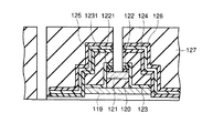
その後、白金膜121上に保護膜122としてAl2O3膜をスパッタ法により形成する。成膜温度は350℃、膜厚は10nmとした。続いて、保護膜122上に加工マスク材としてCVD酸化膜1221を堆積し、光リソグラフィ法とRIE法によって該CVD酸化膜1221をパターンニングしフォトレジストを除去した後、保護膜122、第2の白金膜121、及びPZT膜120をRIE法によってエッチング加工する。 Thereafter, an Al 2 O 3 film is formed as a protective film 122 on the platinum film 121 by sputtering. The film forming temperature was 350 ° C. and the film thickness was 10 nm. Subsequently, a CVD oxide film 1221 is deposited on the protective film 122 as a processing mask material, the CVD oxide film 1221 is patterned by photolithography and RIE, and the photoresist is removed. Then, the protective film 122 and the second film The platinum film 121 and the PZT film 120 are etched by the RIE method.
次に、保護膜123としてAl2O3膜をスパッタ法により形成する。成膜温度は350℃、膜厚は10nmとした。続いて、保護膜123上に加工マスク材としてCVD酸化膜1231を堆積し、光リソグラフィ法とRIE法の組合せによって保護膜123、第1の白金膜119、イリジウム膜118,チタン膜117,炭化ケイ素膜116の順にパターンニング加工を行い、キャパシタの形成を完了する。 Next, an Al 2 O 3 film is formed as the protective film 123 by sputtering. The film forming temperature was 350 ° C. and the film thickness was 10 nm. Subsequently, a CVD oxide film 1231 is deposited on the protective film 123 as a processing mask material, and the protective film 123, the first platinum film 119, the iridium film 118, the titanium film 117, and silicon carbide are combined by a combination of photolithography and RIE. Patterning is performed in the order of the film 116 to complete the formation of the capacitor.
この後、保護膜124としてAl2O3膜をCVD法の一種であるALD法により形成する。成膜温度は200℃、膜厚は10nmとした。続いて、保護膜124上にCVD酸化膜125を50nm堆積し、保護膜126としてAl2O3膜をALD法により形成する。成膜温度は200℃、膜厚は10nmとした。 Thereafter, an Al 2 O 3 film is formed as the protective film 124 by an ALD method which is a kind of CVD method. The film forming temperature was 200 ° C. and the film thickness was 10 nm. Subsequently, a CVD oxide film 125 is deposited to a thickness of 50 nm on the protective film 124, and an Al 2 O 3 film is formed as the protective film 126 by the ALD method. The film forming temperature was 200 ° C. and the film thickness was 10 nm.
次に、全面にCVD酸化膜127を堆積し該キャパシタを覆い、CMPによる平坦化を行い、光リソグラフィ法とRIE法によってCVD酸化膜127をパターンニングし、第2の白金膜121へのコンタクトホール128を形成する。続いて、加工時にPZT膜120に生じたダメージを除去するために、酸素雰囲気下で600℃程度の熱処理を行う。 Next, a CVD oxide film 127 is deposited on the entire surface to cover the capacitor, planarization is performed by CMP, the CVD oxide film 127 is patterned by photolithography and RIE, and a contact hole to the second platinum film 121 is formed. 128 is formed. Subsequently, in order to remove damage caused to the PZT film 120 during processing, a heat treatment is performed at about 600 ° C. in an oxygen atmosphere.
この後、図示しないが、ドライブ線、ビット線の形成、さらに上層メタル配線の工程を経て、FeRAMが完成することになる。 Thereafter, although not shown, the FeRAM is completed through the formation of drive lines and bit lines, and further through the process of the upper metal wiring.
図2は、本実施の形態の製造プロセスにより製造されたFeRAMの主要部を示す断面図である。図2に示すように、第2の白金膜121(上部電極)の上面にスパッタ法による保護膜122が形成され、保護膜122の上側、第2の白金膜121の側面、PZT膜120(誘電体膜)の側面、及び第1の白金膜119(下部電極)の上面に、スパッタ法による保護膜123が形成されている。さらに、保護膜123の上側と第1の白金膜119の側面にALD法による保護膜124が形成され、保護膜124の上側にALD法による保護膜126が形成されている。 FIG. 2 is a cross-sectional view showing the main part of the FeRAM manufactured by the manufacturing process of the present embodiment. As shown in FIG. 2, a protective film 122 is formed on the upper surface of the second platinum film 121 (upper electrode) by sputtering, and the upper side of the protective film 122, the side surface of the second platinum film 121, and the PZT film 120 (dielectric). A protective film 123 is formed on the side surface of the body film and the upper surface of the first platinum film 119 (lower electrode) by sputtering. Further, a protective film 124 by the ALD method is formed on the upper side of the protective film 123 and the side surface of the first platinum film 119, and a protective film 126 by the ALD method is formed on the upper side of the protective film 124.
以上のように、保護膜122,123(第1の保護膜)にスパッタ法により形成したAl2O3膜を使用し、保護膜124,126(第2の保護膜)にALD法により形成したAl2O3膜を使用することにより、加工時、CVD酸化膜の堆積時、さらにはALD法によるAl2O3膜の形成時等に生じるPZT膜120へのダメージを低減することが可能となる。 As described above, the Al 2 O 3 film formed by the sputtering method is used for the protective films 122 and 123 (first protective film), and the ALD method is formed on the protective films 124 and 126 (second protective film). by using the Al 2 O 3 film, during processing, during the deposition of the CVD oxide film, and further can reduce the damage to the PZT film 120 generated the Al 2 O 3 film formation or the like of by the ALD method Become.
なお、本実施の形態においては、保護膜122,123ともにスパッタ膜を使用して形成したが、保護膜122だけにスパッタ膜を使用した場合にも効果が有ることが確認されている。キャパシタ材料としては、強誘電体膜にPZT膜、上下電極に白金を用いたが、このような材料に限定されることはない。たとえば、強誘電体膜としてSBT膜を用いることも可能である。また、電極としてイリジウム、ルテニウム、あるいはストロンチウムルテニウム酸化物のような化合物導電体も使用することが可能である。 In the present embodiment, both the protective films 122 and 123 are formed using a sputtered film. However, it has been confirmed that the sputtered film is effective when only the protective film 122 is used. As a capacitor material, a PZT film is used for the ferroelectric film and platinum is used for the upper and lower electrodes. However, the material is not limited to such a material. For example, an SBT film can be used as the ferroelectric film. Further, a compound conductor such as iridium, ruthenium, or strontium ruthenium oxide can be used as an electrode.
本実施の形態は、FeRAMや高誘電体キャパシタを有するDRAMにおけるキャパシタプロセスのように、キャパシタ形成工程におけるRIEやプラズマCVD工程により生じるダメージを回避または軽減する目的で保護膜を使用する構造において、キャパシタ特性の劣化の極めて少ない新たな半導体装置ならびにその製造方法を提供している。 In this embodiment, a capacitor is used in a structure in which a protective film is used for the purpose of avoiding or reducing damage caused by RIE or plasma CVD process in the capacitor formation process, such as a capacitor process in a DRAM having FeRAM or a high dielectric capacitor. A new semiconductor device with extremely little deterioration in characteristics and a method for manufacturing the same are provided.
本実施の形態では、これらの問題を解決し特性の優れたキャパシタ誘電体膜の形成を可能にしつつ、下地プラグとの熱的安定性を同時に図ることを可能にする。これにより、信頼性の高い微細かつ高集積なFeRAMやDRAMなどの半導体装置を提供することが可能になる。以下に、その効果について具体的に説明する。 In the present embodiment, these problems can be solved and a capacitor dielectric film having excellent characteristics can be formed, and thermal stability with the base plug can be simultaneously achieved. This makes it possible to provide highly reliable semiconductor devices such as fine and highly integrated FeRAM and DRAM. Below, the effect is demonstrated concretely.
Al酸化膜は、耐水素バリア性を有しRIE工程やプラズマCVD工程さらにはシンタ工程からキャパシタ特性の劣化を防ぐ保護膜として有効である。CVD法によるAl酸化膜の成膜は、段差被膜性が良く、特にALD(atomic layer deposition)法は段差被膜性、膜厚制御性に優れている。しかし、ALD法によりAl酸化膜の成膜を行う際には、原料ガスとしてTMA(trymetnyl−Aluminun)を使用するため、キャパシタ上部電極、または強誘電体に直接成膜を行うと、TMAより発生した水素によりキャパシタ特性を劣化させてしまう。 The Al oxide film has a hydrogen barrier property and is effective as a protective film that prevents deterioration of capacitor characteristics from the RIE process, plasma CVD process, and sintering process. The formation of the Al oxide film by the CVD method has good step film property, and in particular, the ALD (atomic layer deposition) method has excellent step film property and film thickness controllability. However, when depositing an Al oxide film by the ALD method, TMA (trimethynyl-aluminun) is used as a source gas, so if the film is deposited directly on the capacitor upper electrode or ferroelectric, it is generated from TMA. The capacitor characteristics are deteriorated by the hydrogen.
しかし本実施の形態のように、キャパシタ上部電極、または強誘電体に直接接する保護膜はスパッタ法を、その上側の保護膜は段差被膜性の良いALD法を用いて形成することにより、水素に対するバリア性が高まり、キャパシタ特性を劣化させること無く、Al酸化膜を保護膜として形成することが可能となり、後工程ダメージを回避して優れた特性を持つ強誘電体キャパシタセルを得ることが可能となる。 However, as in this embodiment, the protective film directly in contact with the capacitor upper electrode or the ferroelectric is formed by the sputtering method, and the protective film on the upper side is formed by the ALD method having a good step film property. The barrier property is enhanced, and it becomes possible to form an Al oxide film as a protective film without deteriorating the capacitor characteristics, and it is possible to obtain a ferroelectric capacitor cell having excellent characteristics by avoiding damages in the subsequent process. Become.
さらに、スパッタ法によりAl酸化膜を形成するときの成膜温度を350℃とすることにより、AL酸化膜である保護膜122,123の構造は、図3に示す断面画像のように粒界を有する柱状構造となる。このときのAl2O3膜の粒径は20〜50nmであった。よって、保護膜122,123における緻密化された柱状構造により、粒界で水素が留まるため水素の透過性が低くなり、バリア性が高まり、後工程のダメージをより低減することが可能となる。なお、柱状構造を形成するための成膜温度の範囲は200℃以上600℃以下である。また、その他の保護膜124,126は、アモルファス構造をなしている。 Further, by forming the Al oxide film at 350 ° C. when the Al oxide film is formed by sputtering, the structure of the protective films 122 and 123, which are AL oxide films, has grain boundaries as shown in the cross-sectional image shown in FIG. It has a columnar structure. The particle size of the Al 2 O 3 film at this time was 20 to 50 nm. Therefore, the dense columnar structures in the protective films 122 and 123 allow hydrogen to remain at the grain boundaries, so that the hydrogen permeability is lowered, the barrier property is increased, and damage in the subsequent process can be further reduced. Note that the range of the film formation temperature for forming the columnar structure is 200 ° C. or more and 600 ° C. or less. The other protective films 124 and 126 have an amorphous structure.
図4は、本実施の形態により製造したFeRAMキャパシタにおけるヒステリシス特性を示す図である。図4から分かるように良好なヒステリシス特性が得られている。 FIG. 4 is a diagram showing hysteresis characteristics in the FeRAM capacitor manufactured according to the present embodiment. As can be seen from FIG. 4, good hysteresis characteristics are obtained.
図5は、FeRAMキャパシタにおけるヒステリシス特性を示す図であり、(a)は全ての保護膜122,123,124,126にCVD法により形成したAl2O3膜を使用した場合、(b)は全ての保護膜122,123,124,126にスパッタ法により形成したAl2O3膜を使用した場合を示す図である。図5の(a),(b)に比べて、図4の本実施の形態によるヒステリシス特性が良好であることが分かる。 FIG. 5 is a diagram showing hysteresis characteristics in an FeRAM capacitor. FIG. 5A shows a case where an Al 2 O 3 film formed by CVD is used for all the protective films 122, 123, 124 and 126, and FIG. is a diagram showing a case of using Al 2 O 3 film was formed by sputtering on all of the protective film 122,123,124,126. It can be seen that the hysteresis characteristics according to the present embodiment shown in FIG. 4 are better than those shown in FIGS.
図5の(a)に示すように全ての保護膜をCVD法により形成する場合、上部電極とPZT膜の側面に直接Al2O3を成膜する際に、CVDプロセスの原料であるTMAによりAl2O3成膜初期にPZTが還元されキャパシタ特性が劣化する。このCVDプロセスのダメージの分だけ、図5の(a)では図4に比べて特性が悪くなっている。 When all the protective films are formed by the CVD method as shown in FIG. 5A, when the Al 2 O 3 film is directly formed on the side surfaces of the upper electrode and the PZT film, TMA which is a raw material of the CVD process is used. PZT is reduced in the initial stage of Al 2 O 3 film formation, and the capacitor characteristics deteriorate. In FIG. 5A, the characteristic is worse than that in FIG. 4 by the amount of the damage of the CVD process.
図5の(b)に示すように全ての保護膜をスパッタ法により形成する場合、CVDプロセスのようなダメージはないが、スパッタAl2O3膜自身のH2バリア性が低いことと段差被膜性が低いことにより、Al2O3を成膜できない部分が発生し、そこからH2が拡散しキャパシタ特性を劣化させてしまう。このバリア性の低い分だけ、図5の(b)では図4に比べて特性が悪くなっている。 When all protective films are formed by sputtering as shown in FIG. 5B, there is no damage as in the CVD process, but the sputtered Al 2 O 3 film itself has low H 2 barrier properties and a step film. Due to the low property, a portion where Al 2 O 3 cannot be formed is generated, and H 2 diffuses from there to deteriorate the capacitor characteristics. Due to this low barrier property, the characteristics in FIG. 5B are worse than those in FIG.
一方、図4の場合は、まずプロセスダメージを受けやすい上部電極とPZT膜の側面に直接Al2O3を成膜する際にスパッタ法を利用し、その上部を成膜する際にALD法を利用してバリア性を高くし完全にキャパシタを覆うことで、後工程のダメージを効果的に防ぐことが可能となる。よって図4では、図5の(a),(b)に比べて良好な特性が得られている。 On the other hand, in the case of FIG. 4, the sputtering method is first used when directly depositing Al 2 O 3 on the side surfaces of the upper electrode and the PZT film which are susceptible to process damage, and the ALD method is used when depositing the upper portion. By utilizing the barrier property and completely covering the capacitor, it is possible to effectively prevent damage in the subsequent process. Therefore, in FIG. 4, better characteristics are obtained than in (a) and (b) of FIG. 5.
以上のように、本実施の形態により微細でかつ高密度・高集積な強誘電体メモリを提供することが可能になる。 As described above, according to this embodiment, it is possible to provide a fine, high-density and highly integrated ferroelectric memory.
なお、本発明は上記実施の形態のみに限定されず、要旨を変更しない範囲で適宜変形して実施できる。たとえば、本発明は強誘電体メモリに限らず強誘電体キャパシタを用いたDRAMにおいても適用できる。 In addition, this invention is not limited only to the said embodiment, In the range which does not change a summary, it can deform | transform suitably and can be implemented. For example, the present invention can be applied not only to a ferroelectric memory but also to a DRAM using a ferroelectric capacitor.
S…Si基板 100…ゲート電極 101…素子分離領域 102…酸化膜 103…多結晶シリコン膜 104…WSix膜 105…窒化膜 106…窒化膜 107…ソース・ドレイン領域 108…CVD酸化膜 109…コンタクトホール 110…TiN膜 111…CVDタングステン 112…CVD窒化膜 113…コンタクトホール 114…TiN膜 115…タングステン 116…炭化ケイ素膜 117…チタン膜 118…イリジウム膜 119…第1の白金膜 120…PZT膜 121…第2の白金膜 122…保護膜 1221…CVD酸化膜 123…保護膜 1231…CVD酸化膜 124…保護膜 125…CVD酸化膜 126…保護膜 127…CVD酸化膜 128…コンタクトホール 200…キャパシタ下部電極 300…キャパシタ誘電体膜 400…キャパシタ上部電極 S ... Si substrate 100 ... gate electrode 101 ... isolation region 102 ... oxide film 103 ... polycrystalline silicon film 104 ... WSi x film 105 ... nitride film 106 ... nitride film 107 ... source-drain regions 108 ... CVD oxide film 109 ... Contacts Hole 110 ... TiN film 111 ... CVD tungsten 112 ... CVD nitride film 113 ... Contact hole 114 ... TiN film 115 ... Tungsten 116 ... Silicon carbide film 117 ... Titanium film 118 ... Iridium film 119 ... First platinum film 120 ... PZT film 121 ... Second platinum film 122 ... Protective film 1221 ... CVD oxide film 123 ... Protective film 1231 ... CVD oxide film 124 ... Protective film 125 ... CVD oxide film 126 ... Protective film 127 ... CVD oxide film 128 ... Contact hole 200 ... Bottom of capacitor Electrode 300 ... Capacity Sita dielectric film 400 ... Upper electrode of capacitor
Claims (8)
前記上部電極の上面のみに接しスパッタ法により成膜された柱状構造をなす第1のAl2O3膜と、
前記上部電極の側面に接し前記第1のAl2O3膜の上側にスパッタ法により成膜された柱状構造をなす第2のAl2O3膜と、
前記第2のAl2O3膜の上側にCVD法により成膜された第3のAl2O3膜と、
前記キャパシタの上方における前記第1のAl 2 O 3 膜と前記第2のAl 2 O 3 膜の間に設けられた第1の膜と、
を備えたことを特徴とする半導体装置。 In a semiconductor device having a capacitor composed of a lower electrode, a dielectric, and an upper electrode,
A first Al 2 O 3 film having a columnar structure formed by sputtering and contacting only the upper surface of the upper electrode;
A second Al 2 O 3 film having a columnar structure that is in contact with a side surface of the upper electrode and formed by sputtering on the upper side of the first Al 2 O 3 film;
A third of the Al 2 O 3 film formed by the CVD method on the upper side of the second Al 2 O 3 film,
A first film provided between the first Al 2 O 3 film and the second Al 2 O 3 film above the capacitor ;
A semiconductor device comprising:
前記上部電極の上面のみに接する第1のAl2O3膜をスパッタ法により成膜し、
前記キャパシタの上方における前記第1のAl 2 O 3 膜の上側に第1の膜を成膜し、
前記第1の膜の上側に前記上部電極の側面に接する第2のAl2O3膜をスパッタ法により成膜し、
前記第2のAl2O3膜の上側に第3のAl2O3膜をCVD法により成膜することを特徴とする半導体装置の製造方法。 In a method for manufacturing a semiconductor device having a capacitor including a lower electrode, a dielectric, and an upper electrode,
Forming a first Al 2 O 3 film in contact with only the upper surface of the upper electrode by sputtering;
Forming a first film on the upper side of the first Al 2 O 3 film above the capacitor ;
A second Al 2 O 3 film in contact with the side surfaces of the upper electrode on the upper side of the first film is formed by sputtering,
A method of manufacturing a semiconductor device, comprising forming a third Al 2 O 3 film on the upper side of the second Al 2 O 3 film by a CVD method.
Priority Applications (2)
| Application Number | Priority Date | Filing Date | Title |
|---|---|---|---|
| JP2004143428A JP4105656B2 (en) | 2004-05-13 | 2004-05-13 | Semiconductor device and manufacturing method thereof |
| US10/856,868 US20050255663A1 (en) | 2004-05-13 | 2004-06-01 | Semiconductor device and method of manufacturing the same |
Applications Claiming Priority (1)
| Application Number | Priority Date | Filing Date | Title |
|---|---|---|---|
| JP2004143428A JP4105656B2 (en) | 2004-05-13 | 2004-05-13 | Semiconductor device and manufacturing method thereof |
Publications (2)
| Publication Number | Publication Date |
|---|---|
| JP2005327847A JP2005327847A (en) | 2005-11-24 |
| JP4105656B2 true JP4105656B2 (en) | 2008-06-25 |
Family
ID=35309956
Family Applications (1)
| Application Number | Title | Priority Date | Filing Date |
|---|---|---|---|
| JP2004143428A Expired - Fee Related JP4105656B2 (en) | 2004-05-13 | 2004-05-13 | Semiconductor device and manufacturing method thereof |
Country Status (2)
| Country | Link |
|---|---|
| US (1) | US20050255663A1 (en) |
| JP (1) | JP4105656B2 (en) |
Families Citing this family (10)
| Publication number | Priority date | Publication date | Assignee | Title |
|---|---|---|---|---|
| JP4284228B2 (en) * | 2004-04-19 | 2009-06-24 | 株式会社東芝 | Manufacturing method of semiconductor device |
| JP2006005234A (en) * | 2004-06-18 | 2006-01-05 | Seiko Epson Corp | Semiconductor device and method of manufacturing the same |
| CN100431155C (en) * | 2004-06-28 | 2008-11-05 | 富士通株式会社 | Semiconductor device and method for fabricating the same |
| JP4497312B2 (en) * | 2004-10-19 | 2010-07-07 | セイコーエプソン株式会社 | Ferroelectric memory manufacturing method |
| JP4953580B2 (en) * | 2005-03-03 | 2012-06-13 | 富士通セミコンダクター株式会社 | Manufacturing method of semiconductor device |
| JP2006310637A (en) * | 2005-04-28 | 2006-11-09 | Toshiba Corp | Semiconductor device |
| KR101287201B1 (en) * | 2005-12-30 | 2013-07-16 | 엘지디스플레이 주식회사 | A electrochromic display device and a method for fabricating the same |
| DE102010024079A1 (en) | 2010-06-17 | 2011-12-22 | Osram Opto Semiconductors Gmbh | Method for producing an optoelectronic semiconductor chip and optoelectronic semiconductor chip |
| JP5672832B2 (en) * | 2010-08-06 | 2015-02-18 | 富士通セミコンダクター株式会社 | Semiconductor device and manufacturing method thereof |
| JP2016012609A (en) * | 2014-06-27 | 2016-01-21 | 東京エレクトロン株式会社 | Etching method |
Family Cites Families (17)
| Publication number | Priority date | Publication date | Assignee | Title |
|---|---|---|---|---|
| US6509601B1 (en) * | 1998-07-31 | 2003-01-21 | Samsung Electronics Co., Ltd. | Semiconductor memory device having capacitor protection layer and method for manufacturing the same |
| US6611014B1 (en) * | 1999-05-14 | 2003-08-26 | Kabushiki Kaisha Toshiba | Semiconductor device having ferroelectric capacitor and hydrogen barrier film and manufacturing method thereof |
| US6534809B2 (en) * | 1999-12-22 | 2003-03-18 | Agilent Technologies, Inc. | Hardmask designs for dry etching FeRAM capacitor stacks |
| KR100323874B1 (en) * | 1999-12-22 | 2002-02-16 | 박종섭 | Method of forming an aluminum oxide film in a semiconductor device |
| US6730951B2 (en) * | 2001-06-25 | 2004-05-04 | Matsushita Electric Industrial Co., Ltd. | Capacitor, semiconductor memory device, and method for manufacturing the same |
| KR100423906B1 (en) * | 2001-08-08 | 2004-03-22 | 삼성전자주식회사 | Ferroelectric memory device amd method of forming the same |
| US20030143853A1 (en) * | 2002-01-31 | 2003-07-31 | Celii Francis G. | FeRAM capacitor stack etch |
| JP2004071932A (en) * | 2002-08-08 | 2004-03-04 | Toshiba Corp | Semiconductor device |
| US6621683B1 (en) * | 2002-09-19 | 2003-09-16 | Infineon Technologies Aktiengesellschaft | Memory cells with improved reliability |
| US7091102B2 (en) * | 2002-12-20 | 2006-08-15 | Samsung Electronics Co., Ltd. | Methods of forming integrated circuit devices having a capacitor with a hydrogen barrier spacer on a sidewall thereof and integrated circuit devices formed thereby |
| KR100532427B1 (en) * | 2003-03-27 | 2005-11-30 | 삼성전자주식회사 | Method for manufacturing ferroelectric memory device |
| US20040206993A1 (en) * | 2003-04-17 | 2004-10-21 | Infineon Technologies Ag | Process for fabrication of ferroelectric devices with reduced hydrogen ion damage |
| US6839220B1 (en) * | 2003-07-18 | 2005-01-04 | Infineon Technologies Ag | Multi-layer barrier allowing recovery anneal for ferroelectric capacitors |
| US7101785B2 (en) * | 2003-07-22 | 2006-09-05 | Infineon Technologies Ag | Formation of a contact in a device, and the device including the contact |
| US7001781B2 (en) * | 2003-09-26 | 2006-02-21 | Infineon Technologies Ag | Method for producing a ferroelectric capacitor that includes etching with hardmasks |
| US7001821B2 (en) * | 2003-11-10 | 2006-02-21 | Texas Instruments Incorporated | Method of forming and using a hardmask for forming ferroelectric capacitors in a semiconductor device |
| JP4522088B2 (en) * | 2003-12-22 | 2010-08-11 | 富士通セミコンダクター株式会社 | Manufacturing method of semiconductor device |
-
2004
- 2004-05-13 JP JP2004143428A patent/JP4105656B2/en not_active Expired - Fee Related
- 2004-06-01 US US10/856,868 patent/US20050255663A1/en not_active Abandoned
Also Published As
| Publication number | Publication date |
|---|---|
| JP2005327847A (en) | 2005-11-24 |
| US20050255663A1 (en) | 2005-11-17 |
Similar Documents
| Publication | Publication Date | Title |
|---|---|---|
| JP4827653B2 (en) | Semiconductor device and manufacturing method thereof | |
| JP5251864B2 (en) | Semiconductor device and manufacturing method thereof | |
| JP4884104B2 (en) | Semiconductor device including capacitor and manufacturing method thereof | |
| US20060183250A1 (en) | Methods of fabricating ferroelectric capacitors utilizing a partial chemical mechanical polishing process | |
| WO2006134664A1 (en) | Semiconductor device and method for manufacturing same | |
| US7573120B2 (en) | Semiconductor device and method of manufacturing the same | |
| JP4105656B2 (en) | Semiconductor device and manufacturing method thereof | |
| JP4845624B2 (en) | Semiconductor device and manufacturing method thereof | |
| US7501675B2 (en) | Semiconductor device and method of manufacturing the same | |
| KR101262432B1 (en) | Method for manufacturing semiconductor devuce | |
| JP2006302976A (en) | Semiconductor device and manufacturing method thereof | |
| US20040130026A1 (en) | Semiconductor device and method of manufacturing the same | |
| JP5487140B2 (en) | Manufacturing method of semiconductor device | |
| JP2006269800A (en) | Semiconductor device | |
| JP4220459B2 (en) | Semiconductor device | |
| JP2009105223A (en) | Semiconductor device, and its manufacturing method | |
| JP2010003741A (en) | Semiconductor device, and method of manufacturing semiconductor device | |
| JP2005093605A (en) | Semiconductor device and its manufacturing method | |
| JP5007723B2 (en) | Semiconductor device including capacitor and manufacturing method thereof | |
| JP2009105388A (en) | Semiconductor device and manufacturing method thereof | |
| JP2005353829A (en) | Semiconductor device and its manufacturing method | |
| JP2005129852A (en) | Semiconductor device | |
| JP5326256B2 (en) | Manufacturing method of semiconductor device | |
| JP2007266023A (en) | Semiconductor device and method of manufacturing same | |
| JP2006134961A (en) | Semiconductor device |
Legal Events
| Date | Code | Title | Description |
|---|---|---|---|
| A977 | Report on retrieval |
Free format text: JAPANESE INTERMEDIATE CODE: A971007 Effective date: 20060804 |
|
| A131 | Notification of reasons for refusal |
Free format text: JAPANESE INTERMEDIATE CODE: A131 Effective date: 20060808 |
|
| A521 | Request for written amendment filed |
Free format text: JAPANESE INTERMEDIATE CODE: A523 Effective date: 20061108 |
|
| A131 | Notification of reasons for refusal |
Free format text: JAPANESE INTERMEDIATE CODE: A131 Effective date: 20071211 |
|
| A521 | Request for written amendment filed |
Free format text: JAPANESE INTERMEDIATE CODE: A523 Effective date: 20080228 |
|
| TRDD | Decision of grant or rejection written | ||
| A01 | Written decision to grant a patent or to grant a registration (utility model) |
Free format text: JAPANESE INTERMEDIATE CODE: A01 Effective date: 20080325 |
|
| A61 | First payment of annual fees (during grant procedure) |
Free format text: JAPANESE INTERMEDIATE CODE: A61 Effective date: 20080327 |
|
| R150 | Certificate of patent or registration of utility model |
Free format text: JAPANESE INTERMEDIATE CODE: R150 |
|
| FPAY | Renewal fee payment (event date is renewal date of database) |
Free format text: PAYMENT UNTIL: 20110404 Year of fee payment: 3 |
|
| LAPS | Cancellation because of no payment of annual fees |