JP4126013B2 - 電子回路、電気接続素子および接触ばね用ハウジング、および電磁シールド・プロセス - Google Patents
電子回路、電気接続素子および接触ばね用ハウジング、および電磁シールド・プロセス Download PDFInfo
- Publication number
- JP4126013B2 JP4126013B2 JP2003509832A JP2003509832A JP4126013B2 JP 4126013 B2 JP4126013 B2 JP 4126013B2 JP 2003509832 A JP2003509832 A JP 2003509832A JP 2003509832 A JP2003509832 A JP 2003509832A JP 4126013 B2 JP4126013 B2 JP 4126013B2
- Authority
- JP
- Japan
- Prior art keywords
- contact
- back plate
- main portion
- recess
- main
- Prior art date
- Legal status (The legal status is an assumption and is not a legal conclusion. Google has not performed a legal analysis and makes no representation as to the accuracy of the status listed.)
- Expired - Fee Related
Links
Images


Classifications
-
- G—PHYSICS
- G06—COMPUTING; CALCULATING OR COUNTING
- G06F—ELECTRIC DIGITAL DATA PROCESSING
- G06F1/00—Details not covered by groups G06F3/00 - G06F13/00 and G06F21/00
- G06F1/16—Constructional details or arrangements
- G06F1/18—Packaging or power distribution
-
- G—PHYSICS
- G06—COMPUTING; CALCULATING OR COUNTING
- G06F—ELECTRIC DIGITAL DATA PROCESSING
- G06F1/00—Details not covered by groups G06F3/00 - G06F13/00 and G06F21/00
- G06F1/16—Constructional details or arrangements
- G06F1/18—Packaging or power distribution
- G06F1/183—Internal mounting support structures, e.g. for printed circuit boards, internal connecting means
- G06F1/185—Mounting of expansion boards
-
- G—PHYSICS
- G06—COMPUTING; CALCULATING OR COUNTING
- G06F—ELECTRIC DIGITAL DATA PROCESSING
- G06F1/00—Details not covered by groups G06F3/00 - G06F13/00 and G06F21/00
- G06F1/16—Constructional details or arrangements
- G06F1/18—Packaging or power distribution
- G06F1/183—Internal mounting support structures, e.g. for printed circuit boards, internal connecting means
- G06F1/184—Mounting of motherboards
-
- G—PHYSICS
- G06—COMPUTING; CALCULATING OR COUNTING
- G06F—ELECTRIC DIGITAL DATA PROCESSING
- G06F1/00—Details not covered by groups G06F3/00 - G06F13/00 and G06F21/00
- G06F1/16—Constructional details or arrangements
- G06F1/18—Packaging or power distribution
- G06F1/183—Internal mounting support structures, e.g. for printed circuit boards, internal connecting means
- G06F1/186—Securing of expansion boards in correspondence to slots provided at the computer enclosure
-
- H—ELECTRICITY
- H05—ELECTRIC TECHNIQUES NOT OTHERWISE PROVIDED FOR
- H05K—PRINTED CIRCUITS; CASINGS OR CONSTRUCTIONAL DETAILS OF ELECTRIC APPARATUS; MANUFACTURE OF ASSEMBLAGES OF ELECTRICAL COMPONENTS
- H05K9/00—Screening of apparatus or components against electric or magnetic fields
- H05K9/0007—Casings
- H05K9/0015—Gaskets or seals
- H05K9/0016—Gaskets or seals having a spring contact
Description
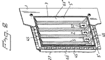
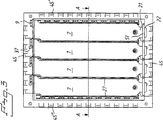
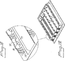
上部および下部に外側部分を有するフレーム・パーツを開口に取り付け、開口の側部に配置された最も外側のフレーム・パーツ、サイド・フレーム・パーツ、および左側または右側の外側部分に取り付ける。これらの外側部分は開口の縁部に接続する。さらに、フレーム・パーツは外側部分で互いに接続する。フレーム・パーツは、開口をバック・プレートを対象とする部分開口に分割することができる。
フレーム・パーツをハウジングに電気接続させ、かつ両側に配置されたフレーム・パーツを互いに電気接続させる。上述の接続手段および接触ばねを使用して、これを達成することができる。
開口内への簡単な挿入動作で、簡単である、差込可能なボードに付属する、またはコネクタだけを担持することができるバック・プレートを挿入する。バック・プレートは、形成された部分開口の別々の1つに挿入される。バック・プレートはそれぞれ別々のフレーム・パーツに取り付けられる。全てのバック・プレートを挿入した後、フレーム・パーツと共に、開口を完全に覆う。
挿入動作によって、バック・プレートをフレーム・パーツに電気接続させる。それによって、対応する挿入動作により、両側に配置される挿入されたバック・プレートを同時に、互いに電気接続させることができる。
Claims (12)
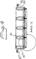
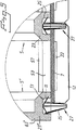
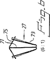
- 差込可能なボードおよび装置ハウジング用の第1のバック・プレートおよびその側部の第2のバック・プレートの間の電気接続用接触素子であって、第1のバックプレートと第2のバックプレートは平行に装置ハウジングに配置され、各々は対向する大きな面とその大きな面に接続する狭い縁面を有しており、
主部分は、装置ハウジングのバックプレート用の開口の側部に設けられた窪みに係合し、
第1のバックプレートが開口に挿入されそして主部分が窪みに係合されたときに、主部分から突出した少なくとも1つの第1の弾性突起が、第1のバックプレートが配置される面に実質的に平行な線であって主部分と交差する線に沿って、第1のバックプレートの狭い縁面とのみ接触し弾性的に作用することを特徴とする接触素子。 - 少なくとも1つの第1の弾性突起が主部分から15°−30°範囲の鋭角で屈曲していることを特徴とする請求項1記載の接触素子。
- 少なくとも1つの第1の弾性突起が実質的に平らであることを特徴とする請求項1記載の接触子。
- 第1のバックプレートが開口に挿入されそして主部分が窪みに係合されているときに、第1の弾性突起が、第1のバックプレートの縁面と良好な点接触を与えるように主部分から垂直に延びる中心線に沿って弱い屈曲を有することを特徴とする請求項1記載の接触素子。
- 主部分が窪みに係合されているとき主部分の一部が窪みの外にも存在するような幅を持っていることを特徴とする請求項1記載の接触素子。
- 主部分がほぼ平らなストリップ形状をしており、主部分の第1の長手縁部から突出している第1の弾性突起を複数有し、その複数の弾性突起は主部分の異なる側に交互に屈曲していることを特徴とする請求項1記載の接触素子。
- 第1の長手縁部の反対側にあって、主部分が窪みに係合しているときに窪みに配置される縁部を第2の長手縁部とすることを特徴とする請求項1記載の接触素子。
- 主部分の第1の長手縁部と反対側の第2の長手縁部から突出し、窪みに主部分を係合するように、窪みに主部分が挿入されたときに窪みの両側に接触するための主部分の異なる側に交互に屈曲する第2の弾性突起を有することを特徴とする請求項6記載の接触素子。
- 第2の弾性突起が平らであること特徴とする請求項8記載の接触素子。
- 第2の弾性突起が、第1の弾性突起と反対側に配置され、第1の弾性突起に対して異なる側に屈曲することを特徴とする請求項8に記載の接触素子。
- 主部分の窪みへ係合するために、主部分が窪みに挿入されたとき主部分から突出した少なくとも1つの第2の弾性突起が窪みの端面内に食い込むことを特徴とする請求項8に記載の接触素子。
- 主部分は、実質的に平らなストリップ形状をしており、そして主部分の第1の長手縁部からの複数の第1の突起を含む少なくとも1つの第1の弾性突起を有し、さらに、主部分は、主部分が窪みに係合されているとき第2の突起は挿入された主部分の一部であって、主部分と同一平面であることを特徴とする請求項1に記載の接触素子。
Applications Claiming Priority (2)
| Application Number | Priority Date | Filing Date | Title |
|---|---|---|---|
| SE0102322A SE523388C2 (sv) | 2001-06-27 | 2001-06-27 | Hölje för elektroniska anordningar med en öppning för instickskort samt kontaktelement för elektrisk förbindning mellan en panel för instickskort och ett apparathölje |
| PCT/SE2002/001292 WO2003003802A1 (en) | 2001-06-27 | 2002-06-27 | Housing for electronic circuits, electrically connecting element and contact spring, procedure for electromagnetic shielding |
Publications (3)
| Publication Number | Publication Date |
|---|---|
| JP2004531095A JP2004531095A (ja) | 2004-10-07 |
| JP2004531095A5 JP2004531095A5 (ja) | 2006-01-05 |
| JP4126013B2 true JP4126013B2 (ja) | 2008-07-30 |
Family
ID=20284671
Family Applications (1)
| Application Number | Title | Priority Date | Filing Date |
|---|---|---|---|
| JP2003509832A Expired - Fee Related JP4126013B2 (ja) | 2001-06-27 | 2002-06-27 | 電子回路、電気接続素子および接触ばね用ハウジング、および電磁シールド・プロセス |
Country Status (9)
| Country | Link |
|---|---|
| US (1) | US7158388B2 (ja) |
| EP (1) | EP1407645B1 (ja) |
| JP (1) | JP4126013B2 (ja) |
| KR (1) | KR20040038920A (ja) |
| CN (1) | CN1331378C (ja) |
| AT (1) | ATE487360T1 (ja) |
| DE (1) | DE60238197D1 (ja) |
| SE (1) | SE523388C2 (ja) |
| WO (1) | WO2003003802A1 (ja) |
Families Citing this family (16)
| Publication number | Priority date | Publication date | Assignee | Title |
|---|---|---|---|---|
| JP2005251309A (ja) * | 2004-03-04 | 2005-09-15 | Hitachi Ltd | ディスクアレイ装置 |
| JP4672599B2 (ja) * | 2006-05-26 | 2011-04-20 | 富士通テレコムネットワークス株式会社 | プラグインユニット板の表示構造 |
| SE533455C2 (sv) * | 2009-10-23 | 2010-10-05 | Clamco Invest Ab | Hölje för elektronisk utrustning, innefattande kontakteringsanordning |
| SE534234C2 (sv) * | 2009-10-23 | 2011-06-07 | Clamco Invest Ab | Hölje för elektronisk utrustning |
| US8270929B1 (en) * | 2011-09-09 | 2012-09-18 | Contech RF Devices, LLC | RF shielding for mobile devices |
| EP3118718B1 (en) * | 2013-02-28 | 2022-12-21 | Oracle International Corporation | Power management of rack-mounted field replaceable units |
| CN104122961A (zh) * | 2013-04-25 | 2014-10-29 | 鸿富锦精密工业(深圳)有限公司 | 机柜式服务器及虚拟服务器机箱 |
| GB2515113B (en) | 2013-06-14 | 2015-12-30 | Eschmann Holdings Ltd | Surgical table and method of operating the same |
| CN104238656A (zh) * | 2013-06-24 | 2014-12-24 | 鸿富锦精密工业(深圳)有限公司 | 扩充卡固定装置 |
| GB2516051B (en) | 2013-07-09 | 2016-06-08 | Eschmann Holdings Ltd | Surgical tables |
| GB2535054B (en) | 2013-07-12 | 2017-01-11 | Eschmann Holdings Ltd | Tabletop sections for surgical tables |
| CN105241293B (zh) * | 2015-10-30 | 2017-05-31 | 成都标建铝业有限公司 | 一种增强散热效果的散热器型材 |
| CN106647444B (zh) * | 2016-10-31 | 2023-08-01 | 国网山东省电力公司莱芜供电公司 | 采用负反馈的电源调节装置及其调节方法 |
| CN109358715B (zh) * | 2018-10-26 | 2021-10-01 | 英业达科技有限公司 | 计算机机壳 |
| BE1026757B1 (de) * | 2018-11-07 | 2020-06-08 | Phoenix Contact Gmbh & Co | Baugruppe eines Elektronikgeräts mit einem Gerätegehäuse und einer Elektronikbaugruppe |
| CN112462862B (zh) * | 2019-09-06 | 2023-04-07 | 英业达科技有限公司 | 用于扩充卡槽口的电磁遮蔽结构及其扩充卡挡板 |
Family Cites Families (11)
| Publication number | Priority date | Publication date | Assignee | Title |
|---|---|---|---|---|
| DE3907412A1 (de) | 1989-03-08 | 1990-09-13 | Ant Nachrichtentech | Gehaeusesystem zur aufnahme von elektrischen einschueben |
| JP3011379B2 (ja) * | 1991-07-17 | 2000-02-21 | 北川工業株式会社 | 電磁波シールド用ガスケット |
| IT1255012B (it) | 1992-03-27 | 1995-10-13 | Italtel Spa | Dispositivo di schermatura elettromagnetica |
| US5957465A (en) * | 1997-06-17 | 1999-09-28 | Sun Microsystems, Inc. | Modular EMC PCI card gasket |
| US5929376A (en) | 1997-06-20 | 1999-07-27 | Tektronix, Inc. | Electromagnetic interference shield and method of manufacturing |
| US5952608A (en) * | 1997-08-11 | 1999-09-14 | Kim; Sun-Ki | Finger strip for shielding electromagnetic wave and front panel assembly mounting the same |
| US6201711B1 (en) | 1999-05-18 | 2001-03-13 | Hewlett-Packard Company | Computer system housing for attenuating electromagnetic inferference (EMI) |
| US6332618B1 (en) * | 1999-09-20 | 2001-12-25 | Telefonaktiebolaget Lm Ericsson (Publ) | Double sided gasket |
| US6403879B1 (en) * | 2000-06-21 | 2002-06-11 | Hewlett-Packard Company | Electronic chassis having an EMI gasket and integral ventilation holes |
| WO2002037920A1 (en) | 2000-11-03 | 2002-05-10 | Instrument Specialities Company, Inc. | Modular shielding of openings with passing cables |
| US6618271B1 (en) * | 2002-04-01 | 2003-09-09 | Gateway, Inc. | EMI shield |
-
2001
- 2001-06-27 SE SE0102322A patent/SE523388C2/sv not_active IP Right Cessation
-
2002
- 2002-06-27 DE DE60238197T patent/DE60238197D1/de not_active Expired - Lifetime
- 2002-06-27 JP JP2003509832A patent/JP4126013B2/ja not_active Expired - Fee Related
- 2002-06-27 AT AT02744059T patent/ATE487360T1/de not_active IP Right Cessation
- 2002-06-27 KR KR10-2003-7017055A patent/KR20040038920A/ko not_active Application Discontinuation
- 2002-06-27 CN CNB028166566A patent/CN1331378C/zh not_active Expired - Fee Related
- 2002-06-27 EP EP02744059A patent/EP1407645B1/en not_active Expired - Lifetime
- 2002-06-27 US US10/481,589 patent/US7158388B2/en not_active Expired - Fee Related
- 2002-06-27 WO PCT/SE2002/001292 patent/WO2003003802A1/en active Application Filing
Also Published As
| Publication number | Publication date |
|---|---|
| KR20040038920A (ko) | 2004-05-08 |
| EP1407645A1 (en) | 2004-04-14 |
| DE60238197D1 (de) | 2010-12-16 |
| US20040196627A1 (en) | 2004-10-07 |
| ATE487360T1 (de) | 2010-11-15 |
| SE523388C2 (sv) | 2004-04-13 |
| SE0102322L (sv) | 2002-12-28 |
| EP1407645B1 (en) | 2010-11-03 |
| CN1547876A (zh) | 2004-11-17 |
| JP2004531095A (ja) | 2004-10-07 |
| US7158388B2 (en) | 2007-01-02 |
| CN1331378C (zh) | 2007-08-08 |
| SE0102322D0 (sv) | 2001-06-27 |
| WO2003003802A1 (en) | 2003-01-09 |
Similar Documents
| Publication | Publication Date | Title |
|---|---|---|
| JP4126013B2 (ja) | 電子回路、電気接続素子および接触ばね用ハウジング、および電磁シールド・プロセス | |
| US7018237B2 (en) | Electrical connector with improved shielding device | |
| US5973926A (en) | Method and apparatus for attaching circuit board to chassis and forming solid ground connection using a single screw | |
| US4762966A (en) | Electromagnetic signal interference shielding gasket apparatus | |
| US6238244B1 (en) | Shielded electrical connector with superposed terminals | |
| US7497717B2 (en) | Land grid array connector having improved cover | |
| US20020142636A1 (en) | Electrical connector assembly utilizing multiple ground planes | |
| JPH0668319A (ja) | 周辺の遮蔽されたデータカード | |
| JP6498409B2 (ja) | コネクタ組立体 | |
| CN203313588U (zh) | 电磁干扰垫片组件以及斜置屏蔽壳体组件 | |
| CN110718815A (zh) | 背板连接器 | |
| US7387536B2 (en) | Electronic part-mounting socket | |
| US7173826B1 (en) | PC card assembly with frame having longitudinal slot | |
| JP2625546B2 (ja) | 機器のカバーのための取付装置 | |
| US7226311B2 (en) | Socket assembly for card | |
| US6688913B2 (en) | Connector assembly structure | |
| US6239358B1 (en) | I/O shield for electronic assemblies | |
| JP2001267016A (ja) | カードコネクタ用カバー及びそれを用いたカードコネクタ組立体 | |
| US9160113B2 (en) | Electrical connector with engaging arms formed on cover | |
| US6179622B1 (en) | Memory card connector | |
| US20150064969A1 (en) | Electrical connector assembly | |
| US20120267489A1 (en) | Connector mounting apparatus with emi shielding clip | |
| KR100191748B1 (ko) | 차폐 덮개 및 이를 사용한 차폐 방법 | |
| JP4715583B2 (ja) | 電子機器ユニットのシールド構造 | |
| JP2895023B2 (ja) | 電子部品の取付構造 |
Legal Events
| Date | Code | Title | Description |
|---|---|---|---|
| A521 | Request for written amendment filed |
Free format text: JAPANESE INTERMEDIATE CODE: A523 Effective date: 20050621 |
|
| A621 | Written request for application examination |
Free format text: JAPANESE INTERMEDIATE CODE: A621 Effective date: 20050621 |
|
| A131 | Notification of reasons for refusal |
Free format text: JAPANESE INTERMEDIATE CODE: A131 Effective date: 20070807 |
|
| A601 | Written request for extension of time |
Free format text: JAPANESE INTERMEDIATE CODE: A601 Effective date: 20071107 |
|
| A602 | Written permission of extension of time |
Free format text: JAPANESE INTERMEDIATE CODE: A602 Effective date: 20071114 |
|
| A601 | Written request for extension of time |
Free format text: JAPANESE INTERMEDIATE CODE: A601 Effective date: 20071207 |
|
| A602 | Written permission of extension of time |
Free format text: JAPANESE INTERMEDIATE CODE: A602 Effective date: 20071214 |
|
| A521 | Request for written amendment filed |
Free format text: JAPANESE INTERMEDIATE CODE: A523 Effective date: 20071221 |
|
| A131 | Notification of reasons for refusal |
Free format text: JAPANESE INTERMEDIATE CODE: A131 Effective date: 20080304 |
|
| A521 | Request for written amendment filed |
Free format text: JAPANESE INTERMEDIATE CODE: A523 Effective date: 20080314 |
|
| TRDD | Decision of grant or rejection written | ||
| A01 | Written decision to grant a patent or to grant a registration (utility model) |
Free format text: JAPANESE INTERMEDIATE CODE: A01 Effective date: 20080415 |
|
| A01 | Written decision to grant a patent or to grant a registration (utility model) |
Free format text: JAPANESE INTERMEDIATE CODE: A01 |
|
| A61 | First payment of annual fees (during grant procedure) |
Free format text: JAPANESE INTERMEDIATE CODE: A61 Effective date: 20080509 |
|
| R150 | Certificate of patent or registration of utility model |
Free format text: JAPANESE INTERMEDIATE CODE: R150 |
|
| FPAY | Renewal fee payment (event date is renewal date of database) |
Free format text: PAYMENT UNTIL: 20110516 Year of fee payment: 3 |
|
| FPAY | Renewal fee payment (event date is renewal date of database) |
Free format text: PAYMENT UNTIL: 20120516 Year of fee payment: 4 |
|
| FPAY | Renewal fee payment (event date is renewal date of database) |
Free format text: PAYMENT UNTIL: 20130516 Year of fee payment: 5 |
|
| LAPS | Cancellation because of no payment of annual fees |