JP4124841B2 - Network analyzer, high frequency characteristic measurement apparatus, and error factor measurement method - Google Patents
Network analyzer, high frequency characteristic measurement apparatus, and error factor measurement method Download PDFInfo
- Publication number
- JP4124841B2 JP4124841B2 JP19418897A JP19418897A JP4124841B2 JP 4124841 B2 JP4124841 B2 JP 4124841B2 JP 19418897 A JP19418897 A JP 19418897A JP 19418897 A JP19418897 A JP 19418897A JP 4124841 B2 JP4124841 B2 JP 4124841B2
- Authority
- JP
- Japan
- Prior art keywords
- reflection coefficient
- short
- load
- open
- error factor
- Prior art date
- Legal status (The legal status is an assumption and is not a legal conclusion. Google has not performed a legal analysis and makes no representation as to the accuracy of the status listed.)
- Expired - Fee Related
Links
- 238000005259 measurement Methods 0.000 title claims description 43
- 238000000691 measurement method Methods 0.000 title claims 3
- 238000000034 method Methods 0.000 claims description 9
- 238000010586 diagram Methods 0.000 description 9
- 230000005540 biological transmission Effects 0.000 description 5
- 239000011159 matrix material Substances 0.000 description 2
- 238000006243 chemical reaction Methods 0.000 description 1
- 238000001514 detection method Methods 0.000 description 1
- 230000000694 effects Effects 0.000 description 1
- 239000012776 electronic material Substances 0.000 description 1
- 230000001360 synchronised effect Effects 0.000 description 1
Images
Landscapes
- Measurement Of Resistance Or Impedance (AREA)
Description
【0001】
【発明の属する技術分野】
この発明は、ネットワーク・アナライザ(Network Analyzer)のキャリブレーション方法に関する。
【0002】
【従来の技術】
先ず、ネットワーク・アナライザについて一般的な説明をする。ネットワーク・アナライザは回路網や電子部品、電子材料の電気的諸量のうちの高周波の周波数特性を測定するものである。正弦波の微少電気信号を発生させてDUT(被測定物)に与え、その反射特性と伝送特性、つまり応答信号をSパラメータで測定し、解析する測定器である。応答信号は、一般に振幅と位相の情報を持つベクトル量であり、複素数である。そこで、この振幅と位相のベクトル量を解析する測定器をベクトル・ネットワーク・アナライザともいう。
【0003】
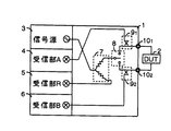
ネットワーク・アナライザの内部構成は周知であるので省略し、Sパラメータ・テストセット内蔵の基本構成を図3に示す。図中、1はSパラメータ・テストセット内蔵ネットワーク・アナライザであり、2はDUT、3は信号源で一般に掃引発振器を用いる。4は受信部Aで、受信信号をミキサで受けて低周波に変換し、アナログ/デジタル変換(A/D)をし、直交検波を行って実数値Rと虚数値Xを求め1つの複素数として測定される。5は受信部Rで信号源3からの送信信号を測定する。6は受信部Bである。これら3つの受信部は信号源3から出力される周波数の信号を検波するように同期されている。
【0004】
7は信号源3からの信号を分離するパワースプリッタで、一方の信号はRFスイッチ8を経てDUT2に与え、他方の信号は受信部R5に与えている。8のRFスイッチは信号源3からの出力信号を端子101 のポート1から出力したり、端子102 のポート2から出力したりするためのものである。91 と92 は端子101 又は端子102 からの応答信号を取り出すブリッジ若しくは方向性結合器である。このSパラメータ・テストセット内蔵ネットワーク・アナライザ1でDUT2のSパラメータを測定する。
【0005】
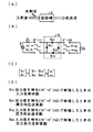
図4を用いてSパラメータを簡単に説明する。測定周波数が高くなり測定系が集中定数的に扱えなくなってくると、図4(A)のように、回路網のパラメータとして入射波・反射波・伝送波を変数として定義し測定する。この定義された回路網のパラメータがSパラメータである。例えば、図4(B)に示すように、信号源3からDUT2のポート1に信号a1を与え、ポート2は特性インピーダンスZoで終端しているとする。このときのS11はポート1における入射波a1と反射波b1の比、S11=b1/a1、として定義され、ポート1における反射係数と呼ばれる。S21はポート1からポート2への伝送波b2とポート1の入射波a1の比、S21=b2/a1、として定義され、ポート1からポート2への伝送係数あるいは透過係数と呼ばれる。S22、S21はポート2から信号a2を与えポート1を特性インピーダンスZoで終端して測定したもので、S22=b2/a2、S12=b1/a2、と定義される。
【0006】
図4(C)はこの関係式をマトリックスで表現したものである。図4(D)はSパラメータの内容の説明である。ネットワーク・アナライザ1は、こうして得られたSパラメータをDUT2のさまざまな特性に換算して表示する。例えば、振幅をdB換算して表示するLOGMAG表示、位相を表示するPHASE表示、群遅延時間の DELAY表示、定在波比の SWR表示、スミスチャートの SMITH表示、ポーラチャートの POLAR表示等である。
ところで、ネットワーク・アナライザ1によりDUT2の反射特性を測定しようとする場合、測定系の誤差によりDUT2の真の値を直接測定することができない。そこで、この誤差の原因を知り、適当なモデルを考えることにより測定値を補正することができる。
【0007】
次に、本発明と関係ある従来のネットワーク・アナライザの測定について、図5を用いて以下説明する。図5(A)はネットワーク・アナライザでDUT2の反射特性を測定する測定系である。信号源3からの信号をDUT2に与え、その反射波をブリッジ9で取り出し受信部A4で測定する。
【0008】
図5(B)にこの場合の測定誤差要因を示す。つまり、測定系の方向性と周波数トラッキングとソース・マッチに主に起因する誤差である。方向性の誤差とは、DUT2に向かう入射信号とDUT2からの反射信号とをブリッジ9で分離しなければならないが、測定値S11mには順方向からのリーケージ、つまり漏れ信号が含まれており、これによる誤差である。周波数トラッキングによる誤差とは、測定系の周波数レスポンスの誤差である。ソース・マッチによる誤差とは、信号源側のインピーダンスと測定システム系のインピーダンスの整合が取れていない場合に、DUT2で反射した信号が信号源3側で再び反射してDUT2に戻り、再反射する。この再反射による誤差である。
【0009】
これらを含めて1ポートの反射特性測定の誤差モデルは、図5(C)のようになる。ここでS11mは測定値、S11aは真値、Ed、Er、Esは誤差要因である。この誤差モデルを、説明は省略するがシグナル・フローグラフで解いてS11mを求めると、図5(D)で表現できる。変形して真値S11aを求めると、図5(E)で表現できる。ここで未知数は、Ed、Er、Esの3つであるから、特性が既知の3つの標準デバイスを用いればこれらの未知数を求めることができる。
【0010】
即ち、 オープン(解放)、ショート(短絡)及びロード(標準負荷Zo)の3つの状態をつくり、それぞれのときのS11mの測定値f( short)、f(open)及びf(load)の値を記録しておき、その値を用いて計算すると、DUT2の真の反射係数S11aを求めることができる。これをキャリブレーションという。つまり、キャリブレーションとは測定系の持つ誤差を予め測定しておき、演算でその影響を取り除くことである。
【0011】
オープン、ショート及びロードの状態をつくるのに校正キットがある。一例を図6に示す。図6(A)は外観図であり、11はコネクタ、12は本体である。図6(B)はオープン素子で端末13は開放されているが、浮遊容量C等が存在するので、位相の補正を加味して反射係数Aopenは(1×ejα)である。図6(C)は ショート素子で端末14は短絡され位相補正を加味して反射係数Ashort は(−1×ejβ)である。図6(D)はロード素子で端末15は特性インピーダンスZoで終端され、反射係数は0と仮定している。特性インピーダンスZoは一般に50Ωヤ75Ωであることが多い。
【0012】
従来のキャリブレーション方法を図2に示す。始めに校正キットのオープン素子の反射係数Aopen=(1×ejα)と、 ショート素子の反射係数Ashort =(−1×ejβ)をネットワーク・アナライザ1の記憶部にメモリする。
次に、ロード素子を無反射、つまり、反射係数=0と仮定して端子10iに接続し、その応答信号を受信部A4で測定する。そのS11mの測定値f(load)は、図5(D)の数式から求め、
f(load)=S11m=Ed+{Er・0/(1ーEs・0)}=Ed
となる。つまり、測定値f(load)=Ed であり、Edが求まる。
【0013】
次に、オープン素子を端子10iに接続しその測定値f(open)を求めてメモリし、 ショート素子を接続しその測定値f( short)を求めてメモリする。ここで、
f(open)=f(load)+{Er・Aopen/(1−Es・Aopen)}
f( short)=f(load)+{Er・Ashort /(1−Es・Ashort )}
であるから、この2式を連立させることにより第二数式を得る。
測定値のf(open)とf( short)が求まると、反射係数のAopenとAshort とを用い、数2の第二数式に従って演算し、EsとErとを求める。
【0014】
【数2】

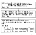
図2に上述した従来のキャリブレーション方法のフローチャートを示す。校正キットのオープン素子とショート素子との反射係数のAopenとAshort をメモリする。ロード素子の反射係数を0と仮定して端子に接続し、信号源から信号を与え、その応答信号を測定すると、その測定値はS11m=f(load)=Edとなり、Edが求まる。同様に測定値f(open)とf( short)を測定し、メモリする。これらのAopenとAshortとf(open)とf( short)とを用いて第二数式に従って演算し、EsとErとを求めて、キャリブレーションを行う。
【0016】
【発明が解決しようとする課題】
従来のキャリブレーション方法では、校正キットのロード素子を反射係数=0と仮定して行っていた。そこで、無反射ロード素子の開発に力をそそいでいた。つまり、ロード素子が理想的と仮定するしか手がなく反射係数=0としていたが、現実には若干の反射がある。従って、このロード素子の理想的でない分がキャリブレーションにおける誤差となり、若干の測定誤差を生じさせていた。
【0017】
この発明は、ロード素子の反射係数を0と仮定せず、反射係数=ρ の既知の値とし、これより測定誤差を生じさせない誤差要因を取得するという、新たなキャリブレーションの方法を提供することを目的とする。
【0018】
【課題を解決するための手段】
上記目的を達成するために、この発明は、既知の反射係数を有する校正キットを使用する。校正キットにはオープン素子とショート素子とロード素子の3種類の素子が準備されている。このそれぞれの素子の反射係数、つまり、オープン素子の反射係数Aopenとショート素子の反射係数Ashort とロード素子の反射係数Aloadとをネットワーク・アナライザの記憶部にメモリする。
【0019】
次に、オープン素子をネットワーク・アナライザの入出力端子に接続し、信号源より信号を送り、その応答信号を受信部A4若しくは受信部B6で測定する。その測定したS11mの測定値をf(open)とする。ショート素子を端子に接続して測定したS11mの測定値をf(short )とする。ロード素子を端子に接続して測定したS11mの測定値をf(load)とする。この測定したf(open)とf(short )とf(load)もネットワーク・アナライザの記憶部にメモリする。
【0020】
次に、上記の反射係数Aopen、Ashort 、Aload、と上記の測定値f(open)、f(short )、f(load)、とを用い、数1の第一数式に従って演算部でEd、Es及びErを求めてキャリブレーションを行うものである。
【0021】
【数3】
【発明の実施の形態】
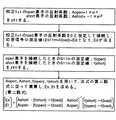
発明の実施の形態を実施例に基づき図面を参照して説明する。図1に本発明のキャリブレーション方法の一実施例のフローチャートを示す。校正キットの3つの素子の反射係数は、理想的にはオープン素子でAopen=1、ショート素子でAshort =−1、ロード素子でAload=0である。ところが、現実には理想的ではなく、若干の誤差がある。そこで事前に正確に測定するか、理論的に計算するか、補正済みのものを購入するかして補正値α、β、ρを明確にしておく。反射係数はオープン素子でAopen=(1×ejα)、ショート素子でAshort =(−1×ejβ)、ロード素子でAload=ρである。この反射係数をネットワーク・アナライザの記憶部にメモリさせる。
【0023】
次に、これらの3つの素子を、図5(A)の入出力端子10iに交互に接続して信号源3より信号を与え、その応答信号を受信部A4で測定する。オープン素子を接続したときのS11mの測定値をf(open)とし、ショート素子を接続したときのS11mの測定値をf(short )、ロード素子を接続したときのS11mの測定値をf(load)として記憶部にメモリさせる。
【0024】
ところで、図5(D)の数式は、
S11m=Ed+{Er・S11a/(1ーEs・S11a)} であるので、この数式を変形すると、
S11m=Ed+S11a(Er−Ed・Es)+S11a・S11m・Es となる。ここで、S11mに上述した測定値を、S11aに反射係数を代入すると、次の3つの式を得る。
f(open)=Ed+Aopen(Er−Ed・Es)+Aopen・f(open)・Es
f(short)=Ed+Ashort(Er−Ed・Es)+Ashort・f(short)・Es
f(load)=Ed+Aload(Er−Ed・Es)+Aload・f(load)・Es
この3つの式をマトリックス表示したのが、数1の第一数式である。この3つの式を演算部で演算して、未知数のEd、Es及びErを求めることができる。つまり、Aload=0と仮定することなくキャリブレーションをすることができる。
【0025】
【発明の効果】
以上詳細に説明したように、この発明は、ロード素子(別名ロードスタンダード)の反射係数が0、つまり理想的な無反射でなくとも、その値が既知であれば演算によってキャリブレーションが可能になった。よって、ロード素子の作製が容易になり、測定誤差の要因が無くなり、ネットワーク・アナライザの利用価値が高まった。この発明の技術的価値は大である。
【図面の簡単な説明】
【図1】本発明のキャリブレーション方法の一実施例のフローチャートである。
【図2】従来のキャリブレーション方法のフローチャートである。
【図3】Sパラメータ・テストセット内蔵ネットワーク・アナライザの一例の構成図である。
【図4】Sパラメータの説明図である。(A)は入射波・反射波・伝送波の説明図、(B)は個々のSパラメータの説明図、(C)はSパラメータの関係式、(D)は個々のSパラメータの説明である。
【図5】1ポート反射特性測定の説明図である。(A)は構成図、(B)は測定誤差の説明図、(C)は誤差モデル図、(D)は測定値S11mの関係式、(E)は真値S11aの関係式である。
【図6】校正キットの説明図である。(A)は外観図、(B)はオープン素子、(C)はショート素子、(D)はロード素子である。
【符号の説明】
1 Sパラメータ・テストセット内蔵ネットワーク・アナライザ
2 DUT(被測定物)
3 信号源
4 受信部A
5 受信部R
6 受信部B
7 パワースプリッタ
8 RFスイッチ
9i、91 、92 ブリッジ若しくは方向性結合器
10i、101 、102 端子
11 コネクタ
12 本体
13 オープン素子端末
14 ショート素子端末
15 ロード素子端末[0001]
BACKGROUND OF THE INVENTION
The present invention relates to a calibration method for a network analyzer.
[0002]
[Prior art]
First, a general description of the network analyzer will be given. The network analyzer measures frequency characteristics of a high frequency among electrical quantities of circuit networks, electronic components, and electronic materials. This is a measuring device that generates a sine wave minute electric signal and applies it to a DUT (device under test), and measures and analyzes its reflection characteristic and transmission characteristic, that is, a response signal using S parameters. The response signal is generally a vector quantity having amplitude and phase information, and is a complex number. Therefore, a measuring device that analyzes the vector quantity of the amplitude and phase is also called a vector network analyzer.
[0003]
Since the internal configuration of the network analyzer is well known, it is omitted, and the basic configuration with a built-in S parameter test set is shown in FIG. In the figure, 1 is a network analyzer with an S-parameter test set, 2 is a DUT, 3 is a signal source, and generally uses a swept oscillator. 4 is a receiving unit A, which receives a received signal with a mixer, converts it to a low frequency, performs analog / digital conversion (A / D), performs quadrature detection, and obtains a real value R and an imaginary value X as one complex number. Measured. Reference numeral 5 denotes a receiving unit R that measures a transmission signal from the signal source 3.
[0004]
Reference numeral 7 denotes a power splitter for separating the signal from the signal source 3. One signal is given to the
[0005]
The S parameter will be briefly described with reference to FIG. When the measurement frequency becomes high and the measurement system can no longer handle the lumped constant, as shown in FIG. 4A, the incident wave, the reflected wave, and the transmitted wave are defined as variables as the parameters of the circuit network and measured. The defined network parameter is the S parameter. For example, as shown in FIG. 4B, it is assumed that the signal a1 is given from the signal source 3 to the
[0006]
FIG. 4C represents this relational expression in a matrix. FIG. 4D illustrates the contents of the S parameter. The
By the way, when the reflection characteristic of the
[0007]
Next, measurement of a conventional network analyzer related to the present invention will be described below with reference to FIG. FIG. 5A shows a measurement system that measures the reflection characteristics of the
[0008]
FIG. 5B shows the measurement error factors in this case. That is, it is an error mainly caused by the directionality of the measurement system, frequency tracking, and source match. The directionality error means that the incident signal directed to DUT2 and the reflected signal from DUT2 must be separated by bridge 9, but the measured value S11m includes leakage from the forward direction, that is, a leakage signal. This is an error. The error due to frequency tracking is an error in the frequency response of the measurement system. The error due to source match means that when the impedance of the signal source side and the impedance of the measurement system system are not matched, the signal reflected by the
[0009]
Including these, the error model for measuring the reflection characteristics of one port is as shown in FIG. Here, S11m is a measured value, S11a is a true value, and Ed, Er, and Es are error factors. Although the explanation of this error model is omitted, it can be expressed by FIG. 5D when S11m is obtained by solving with a signal flow graph. If the true value S11a is obtained by deformation, it can be expressed in FIG. Here, since there are three unknowns, Ed, Er, and Es, these three unknowns can be obtained by using three standard devices with known characteristics.
[0010]
That is, three states of open (release), short (short-circuit) and load (standard load Zo) are created, and the measured values f (short), f (open) and f (load) of S11m at each time are obtained. If it is recorded and calculated using the value, the true reflection coefficient S11a of DUT2 can be obtained. This is called calibration. That is, the calibration is to measure an error of the measurement system in advance and remove the influence by calculation.
[0011]
There are calibration kits to create open, short and load conditions. An example is shown in FIG. FIG. 6A is an external view, 11 is a connector, and 12 is a main body. FIG. 6B is an open element, and the terminal 13 is open, but the stray capacitance C and the like exist, so the reflection coefficient Aopen is (1 × e j α) in consideration of phase correction. FIG. 6C shows a short element, the terminal 14 is short-circuited, and the reflection coefficient Ashort is (−1 × e j β) in consideration of phase correction. FIG. 6D assumes that the load element is a load element, the terminal 15 is terminated with a characteristic impedance Zo, and the reflection coefficient is zero. In general, the characteristic impedance Zo is often 50Ω and 75Ω.
[0012]
A conventional calibration method is shown in FIG. First, the reflection coefficient Aopen = (1 × e j α) of the open element of the calibration kit and the reflection coefficient Ashort = (− 1 × e j β) of the short element are stored in the storage unit of the
Next, assuming that the load element is non-reflective, that is, the reflection coefficient = 0, the load element is connected to the
f (load) = S11m = Ed + {Er · 0 / (1−Es · 0)} = Ed
It becomes. That is, the measured value f (load) = Ed, and Ed is obtained.
[0013]
Next, an open element is connected to the
f (open) = f (load) + {Er · Aopen / (1−Es · Aopen)}
f (short) = f (load) + {Er · Ashort / (1−Es · Ashort)}
Therefore, the second equation is obtained by combining these two equations.
When the measurement values f (open) and f (short) are obtained, the reflection coefficients Aopen and Ashort are used to perform the calculation according to the second equation of
[0014]
[Expression 2]
FIG. 2 shows a flowchart of the conventional calibration method described above. Memorize the reflection coefficients Aopen and Ashort of the open and short elements of the calibration kit. When the load element is assumed to have a reflection coefficient of 0 and connected to a terminal, a signal is applied from a signal source, and the response signal is measured, the measured value is S11m = f (load) = Ed, and Ed is obtained. Similarly, the measurement values f (open) and f (short) are measured and stored. Using these Aopen, Ashort, f (open), and f (short), calculation is performed according to the second formula to obtain Es and Er, and calibration is performed.
[0016]
[Problems to be solved by the invention]
In the conventional calibration method, the load element of the calibration kit is assumed to have a reflection coefficient = 0. Therefore, he was eager to develop a non-reflective load element. In other words, the load element is only assumed to be ideal, and the reflection coefficient = 0, but in reality there is some reflection. Therefore, the non-ideal part of the load element becomes an error in calibration, causing a slight measurement error.
[0017]
The present invention provides a new calibration method in which the reflection coefficient of the load element is not assumed to be 0, the reflection coefficient = ρ is a known value, and an error factor that does not cause a measurement error is obtained. With the goal.
[0018]
[Means for Solving the Problems]
In order to achieve the above object, the present invention uses a calibration kit having a known reflection coefficient. The calibration kit includes three types of elements: open elements, short elements, and load elements. The reflection coefficient of each element, that is, the reflection coefficient Aopen of the open element, the reflection coefficient Ashort of the short element, and the reflection coefficient Aload of the load element are stored in the storage unit of the network analyzer.
[0019]
Next, the open element is connected to the input / output terminal of the network analyzer, a signal is sent from the signal source, and the response signal is measured by the receiving unit A4 or the receiving unit B6. The measured value of S11m is f (open). The measured value of S11m measured with the short element connected to the terminal is defined as f (short). The measured value of S11m measured with the load element connected to the terminal is defined as f (load). The measured f (open), f (short) and f (load) are also stored in the storage unit of the network analyzer.
[0020]
Next, using the above reflection coefficients Aopen, Ashort, Aload and the above measured values f (open), f (short), f (load), Ed, Es in the arithmetic unit according to the first formula of
[0021]
[Equation 3]
DETAILED DESCRIPTION OF THE INVENTION
DESCRIPTION OF THE PREFERRED EMBODIMENTS Embodiments of the present invention will be described based on examples with reference to the drawings. FIG. 1 shows a flowchart of an embodiment of the calibration method of the present invention. The reflection coefficients of the three elements of the calibration kit are ideally Aopen = 1 for an open element, Ashort = −1 for a short element, and Aload = 0 for a load element. However, in reality it is not ideal and there are some errors. Therefore, the correction values α, β, and ρ are clarified by accurately measuring in advance, theoretically calculating, or purchasing a corrected one. The reflection coefficient is Aopen = (1 × e j α) for the open element, Ashort = (− 1 × e j β) for the short element, and Aload = ρ for the load element. This reflection coefficient is stored in the storage unit of the network analyzer.
[0023]
Next, these three elements are alternately connected to the input /
[0024]
By the way, the mathematical formula in FIG.
S11m = Ed + {Er · S11a / (1−Es · S11a)}
S11m = Ed + S11a (Er-Ed.Es) + S11a.S11m.Es. Here, substituting the measurement value described above for S11m and the reflection coefficient for S11a, the following three equations are obtained.
f (open) = Ed + Aopen (Er-Ed · Es) + Aopen · f (open) · Es
f (short) = Ed + Ashort (Er-Ed · Es) + Ashort · f (short) · Es
f (load) = Ed + Aload (Er-Ed · Es) + Aload · f (load) · Es
The first equation of
[0025]
【The invention's effect】
As described above in detail, according to the present invention, even if the reflection coefficient of the load element (also called load standard) is 0, that is, it is not ideal non-reflection, calibration is possible by calculation if the value is known. It was. Therefore, the load element can be easily manufactured, the cause of the measurement error is eliminated, and the utility value of the network analyzer is increased. The technical value of this invention is great.
[Brief description of the drawings]
FIG. 1 is a flowchart of an embodiment of a calibration method of the present invention.
FIG. 2 is a flowchart of a conventional calibration method.
FIG. 3 is a configuration diagram of an example of a network analyzer with a built-in S-parameter test set.
FIG. 4 is an explanatory diagram of S parameters. (A) is an explanatory diagram of incident waves, reflected waves, and transmitted waves, (B) is an explanatory diagram of individual S parameters, (C) is a relational expression of S parameters, and (D) is an explanation of individual S parameters. .
FIG. 5 is an explanatory diagram of 1-port reflection characteristic measurement. (A) is a configuration diagram, (B) is an explanatory diagram of measurement error, (C) is an error model diagram, (D) is a relational expression of measurement value S11m, and (E) is a relational expression of true value S11a.
FIG. 6 is an explanatory diagram of a calibration kit. (A) is an external view, (B) is an open element, (C) is a short element, and (D) is a load element.
[Explanation of symbols]
1 S-parameter test set built-in
3 Signal
5 Receiver R
6 Receiver B
7 power splitter 8 RF switch 9i, 9 1 , 9 2 bridge or
Claims (3)
オープン状態をつくるオープン素子、ショート状態をつくるショート素子およびロード状態をつくるロード素子の既知の反射係数を記録する既知反射係数記録部と、
前記オープン素子、前記ショート素子および前記ロード素子の反射係数の、前記ネットワーク・アナライザによる測定結果を記録する測定反射係数記録部と、
前記ネットワーク・アナライザの方向性に主に起因する誤差の誤差要因Edを、前記オープン素子、前記ショート素子および前記ロード素子の前記既知の反射係数と、前記オープン素子、前記ショート素子および前記ロード素子の前記反射係数の測定結果とに基づき演算する方向性誤差要因演算部と、
ソース・マッチに主に起因する誤差の誤差要因Esを、前記オープン素子、前記ショート素子および前記ロード素子の前記既知の反射係数と、前記オープン素子、前記ショート素子および前記ロード素子の前記反射係数の測定結果とに基づき演算するソースマッチ誤差要因演算部と、
周波数トラッキングに主に起因する誤差の誤差要因Erを、前記オープン素子、前記ショート素子および前記ロード素子の前記既知の反射係数と、前記オープン素子、前記ショート素子および前記ロード素子の前記反射係数の測定結果と、前記誤差要因EdおよびEsに基づき演算する周波数トラッキング誤差要因演算部と、
を備え、
前記オープン素子の前記既知の反射係数をAopen、
前記ショート素子の前記既知の反射係数をAshort、
前記ロード素子の前記既知の反射係数をAload、
前記オープン素子の前記反射係数の測定結果をf(open)、
前記ショート素子の前記反射係数の測定結果をf(short)、
前記ロード素子の前記反射係数の測定結果をf(load)、
とした場合、
前記方向性誤差要因演算部、前記ソースマッチ誤差要因演算部および前記周波数トラッキング誤差要因演算部は、数1の第一数式に従って演算を行う、
A known reflection coefficient recording unit for recording a known reflection coefficient of an open element that creates an open state, a short element that creates a short state, and a load element that creates a load state;
A measurement reflection coefficient recording unit for recording a measurement result of the reflection coefficient of the open element, the short element, and the load element by the network analyzer ;
The error factor Ed of the error mainly caused by the directionality of the network analyzer is the known reflection coefficient of the open element, the short element, and the load element, and the open element, the short element, and the load element. A directional error factor calculation unit that calculates based on the measurement result of the reflection coefficient;
An error factor Es of an error mainly caused by a source match is calculated using the known reflection coefficient of the open element, the short element, and the load element, and the reflection coefficient of the open element, the short element, and the load element. A source match error factor calculation unit that calculates based on the measurement result;
An error factor Er of an error mainly caused by frequency tracking is measured for the known reflection coefficient of the open element, the short element, and the load element, and the reflection coefficient of the open element, the short element, and the load element. A frequency tracking error factor calculation unit that calculates based on the result and the error factors Ed and Es;
With
Aopen for the known reflection coefficient of the open element,
The known reflection coefficient of the short element is Ashort,
Aload for the known reflection coefficient of the load element;
The measurement result of the reflection coefficient of the open element is f (open),
The measurement result of the reflection coefficient of the short element is f (short),
The measurement result of the reflection coefficient of the load element is f (load),
If
The directional error factor calculation unit, the source match error factor calculation unit, and the frequency tracking error factor calculation unit perform calculation according to the first formula of Equation 1.
オープン状態をつくるオープン素子、ショート状態をつくるショート素子およびロード状態をつくるロード素子の既知の反射係数を記録する既知反射係数記録部と、
前記オープン素子、前記ショート素子および前記ロード素子の反射係数の、前記高周波周波数特性測定装置による測定結果を記録する測定反射係数記録部と、
前記高周波周波数特性測定装置の方向性に主に起因する誤差の誤差要因Edを、前記オープン素子、前記ショート素子および前記ロード素子の前記既知の反射係数と、前記オープン素子、前記ショート素子および前記ロード素子の前記反射係数の測定結果とに基づき演算する方向性誤差要因演算部と、
ソース・マッチに主に起因する誤差の誤差要因Esを、前記オープン素子、前記ショート素子および前記ロード素子の前記既知の反射係数と、前記オープン素子、前記ショート素子および前記ロード素子の前記反射係数の測定結果とに基づき演算するソースマッチ誤差要因演算部と、
周波数トラッキングに主に起因する誤差の誤差要因Erを、前記オープン素子、前記ショート素子および前記ロード素子の前記既知の反射係数と、前記オープン素子、前記ショート素子および前記ロード素子の前記反射係数の測定結果と、前記誤差要因EdおよびEsに基づき演算する周波数トラッキング誤差要因演算部と、
を備え、
前記オープン素子の前記既知の反射係数をAopen、
前記ショート素子の前記既知の反射係数をAshort、
前記ロード素子の前記既知の反射係数をAload、
前記オープン素子の前記反射係数の測定結果をf(open)、
前記ショート素子の前記反射係数の測定結果をf(short)、
前記ロード素子の前記反射係数の測定結果をf(load)、
とした場合、
前記方向性誤差要因演算部、前記ソースマッチ誤差要因演算部および前記周波数トラッキング誤差要因演算部は、数2の第一数式に従って演算を行う、
A known reflection coefficient recording unit for recording a known reflection coefficient of an open element that creates an open state, a short element that creates a short state, and a load element that creates a load state;
A measurement reflection coefficient recording unit for recording a measurement result of the reflection coefficient of the open element, the short element, and the load element by the high frequency characteristic measurement device ;
The error factor Ed of the error mainly caused by the directivity of the high-frequency frequency characteristic measuring device is the known reflection coefficient of the open element, the short element, and the load element, and the open element, the short element, and the load. A directional error factor calculation unit for calculating based on the measurement result of the reflection coefficient of the element;
An error factor Es of an error mainly caused by a source match is calculated using the known reflection coefficient of the open element, the short element, and the load element, and the reflection coefficient of the open element, the short element, and the load element. A source match error factor calculation unit that calculates based on the measurement result;
An error factor Er of an error mainly caused by frequency tracking is measured for the known reflection coefficient of the open element, the short element, and the load element, and the reflection coefficient of the open element, the short element, and the load element. A frequency tracking error factor calculation unit that calculates based on the result and the error factors Ed and Es;
With
Aopen for the known reflection coefficient of the open element,
The known reflection coefficient of the short element is Ashort,
Aload for the known reflection coefficient of the load element;
The measurement result of the reflection coefficient of the open element is f (open),
The measurement result of the reflection coefficient of the short element is f (short),
The measurement result of the reflection coefficient of the load element is f (load),
If
The directional error factor calculation unit, the source match error factor calculation unit, and the frequency tracking error factor calculation unit perform calculations according to the first formula of Equation 2 ,
オープン状態をつくるオープン素子、ショート状態をつくるショート素子およびロード状態をつくるロード素子の既知の反射係数を記録する既知反射係数記録工程と、
前記オープン素子、前記ショート素子および前記ロード素子の反射係数の、前記高周波周波数特性測定装置による測定結果を記録する測定反射係数記録工程と、
前記高周波周波数特性測定装置の方向性に主に起因する誤差の誤差要因Edを、前記オープン素子、前記ショート素子および前記ロード素子の前記既知の反射係数と、前記オープン素子、前記ショート素子および前記ロード素子の前記反射係数の測定結果とに基づき演算する方向性誤差要因演算工程と、
ソース・マッチに主に起因する誤差の誤差要因Esを、前記オープン素子、前記ショート素子および前記ロード素子の前記既知の反射係数と、前記オープン素子、前記ショート素子および前記ロード素子の前記反射係数の測定結果とに基づき演算するソースマッチ誤差要因演算工程と、
周波数トラッキングに主に起因する誤差の誤差要因Erを、前記オープン素子、前記ショート素子および前記ロード素子の前記既知の反射係数と、前記オープン素子、前記ショート素子および前記ロード素子の前記反射係数の測定結果と、前記誤差要因EdおよびEsに基づき演算する周波数トラッキング誤差要因演算工程と、
を備え、
前記オープン素子の前記既知の反射係数をAopen、
前記ショート素子の前記既知の反射係数をAshort、
前記ロード素子の前記既知の反射係数をAload、
前記オープン素子の前記反射係数の測定結果をf(open)、
前記ショート素子の前記反射係数の測定結果をf(short)、
前記ロード素子の前記反射係数の測定結果をf(load)、
とした場合、
前記方向性誤差要因演算工程、前記ソースマッチ誤差要因演算工程および前記周波数トラッキング誤差要因演算工程は、数3の第一数式に従って演算を行う、
A known reflection coefficient recording step of recording a known reflection coefficient of an open element that creates an open state, a short element that creates a short state, and a load element that creates a load state;
A measurement reflection coefficient recording step for recording a measurement result of the reflection coefficient of the open element, the short element, and the load element by the high frequency characteristic measuring device ;
The error factor Ed of the error mainly caused by the directivity of the high-frequency frequency characteristic measuring device is the known reflection coefficient of the open element, the short element, and the load element, and the open element, the short element, and the load. A directional error factor calculation step for calculating based on the measurement result of the reflection coefficient of the element;
An error factor Es of an error mainly caused by a source match is calculated using the known reflection coefficient of the open element, the short element, and the load element, and the reflection coefficient of the open element, the short element, and the load element. Source match error factor calculation process that calculates based on the measurement result;
An error factor Er of an error mainly caused by frequency tracking is measured for the known reflection coefficient of the open element, the short element, and the load element, and the reflection coefficient of the open element, the short element, and the load element. A frequency tracking error factor calculation step to calculate based on the result and the error factors Ed and Es;
With
Aopen for the known reflection coefficient of the open element,
The known reflection coefficient of the short element is Ashort,
Aload for the known reflection coefficient of the load element;
The measurement result of the reflection coefficient of the open element is f (open),
The measurement result of the reflection coefficient of the short element is f (short),
The measurement result of the reflection coefficient of the load element is f (load),
If
The directional error factor calculation step , the source match error factor calculation step, and the frequency tracking error factor calculation step perform calculations according to the first equation of Equation 3 .
Priority Applications (1)
| Application Number | Priority Date | Filing Date | Title |
|---|---|---|---|
| JP19418897A JP4124841B2 (en) | 1997-07-18 | 1997-07-18 | Network analyzer, high frequency characteristic measurement apparatus, and error factor measurement method |
Applications Claiming Priority (1)
| Application Number | Priority Date | Filing Date | Title |
|---|---|---|---|
| JP19418897A JP4124841B2 (en) | 1997-07-18 | 1997-07-18 | Network analyzer, high frequency characteristic measurement apparatus, and error factor measurement method |
Publications (2)
| Publication Number | Publication Date |
|---|---|
| JPH1138054A JPH1138054A (en) | 1999-02-12 |
| JP4124841B2 true JP4124841B2 (en) | 2008-07-23 |
Family
ID=16320416
Family Applications (1)
| Application Number | Title | Priority Date | Filing Date |
|---|---|---|---|
| JP19418897A Expired - Fee Related JP4124841B2 (en) | 1997-07-18 | 1997-07-18 | Network analyzer, high frequency characteristic measurement apparatus, and error factor measurement method |
Country Status (1)
| Country | Link |
|---|---|
| JP (1) | JP4124841B2 (en) |
Cited By (1)
| Publication number | Priority date | Publication date | Assignee | Title |
|---|---|---|---|---|
| US20240175959A1 (en) * | 2018-09-29 | 2024-05-30 | Keysight Technologies, Inc. | Integrated vector network analyzer |
Families Citing this family (18)
| Publication number | Priority date | Publication date | Assignee | Title |
|---|---|---|---|---|
| JP2001153904A (en) | 1999-11-25 | 2001-06-08 | Advantest Corp | Network analyzer, network analyzing method and storage medium |
| JP4255017B2 (en) | 2002-04-17 | 2009-04-15 | 株式会社アドバンテスト | Automatic calibrator, calibration method, program and recording medium |
| DE10393797T5 (en) * | 2002-11-27 | 2005-12-01 | Advantest Corp. | Power supply device, method, program, recording medium, network analyzer, and spectrum analyzer |
| JP4506154B2 (en) * | 2003-01-08 | 2010-07-21 | 凸版印刷株式会社 | Characteristic impedance measuring method and measuring apparatus |
| JP4274462B2 (en) | 2003-09-18 | 2009-06-10 | 株式会社アドバンテスト | Error factor acquisition apparatus, method, program, and recording medium |
| JP5242881B2 (en) | 2004-02-23 | 2013-07-24 | ローデ ウント シュワルツ ゲーエムベーハー ウント コー カーゲー | Network analyzer, network analysis method, program, and recording medium |
| JP4462979B2 (en) | 2004-03-26 | 2010-05-12 | 株式会社アドバンテスト | Network analyzer, transmission tracking measurement method, network analysis method, program, and recording medium |
| JPWO2005111635A1 (en) * | 2004-05-14 | 2008-03-27 | 松下電器産業株式会社 | Method and apparatus for measuring electric circuit parameters |
| KR100840923B1 (en) | 2004-06-28 | 2008-06-24 | 가부시키가이샤 아드반테스트 | Devices, methods, programs, recording media and network analyzers, semiconductor test equipment |
| CN100495046C (en) | 2004-06-28 | 2009-06-03 | 株式会社爱德万测试 | Fixture characteristic measurement device, method, network analyzer, and semiconductor test device |
| TW200817688A (en) | 2006-08-30 | 2008-04-16 | Advantest Corp | Element judging device, method, program, recording medium and measuring device |
| JP4188396B2 (en) | 2006-08-31 | 2008-11-26 | 株式会社アドバンテスト | Error factor determination apparatus, method, program, recording medium, output correction apparatus including the apparatus, and reflection coefficient measurement apparatus |
| US7809216B2 (en) * | 2007-03-16 | 2010-10-05 | Photonic Systems, Inc. | Bi-directional signal interface and apparatus using same |
| US7616007B2 (en) * | 2007-07-23 | 2009-11-10 | Advantest Corporation | Device, method, program, and recording medium for error factor measurement, and output correction device and reflection coefficient measurement device provided with the device for error factor measurement |
| US7761253B2 (en) * | 2007-07-23 | 2010-07-20 | Advantest Corporation | Device, method, program, and recording medium for error factor measurement, and output measurement device and input measurement device provided with the device for error factor measurement |
| US10684317B2 (en) * | 2017-09-04 | 2020-06-16 | Rohde & Schwarz Gmbh & Co. Kg | Vector network analyzer and measuring method for frequency-converting measurements |
| JP7721843B2 (en) * | 2021-10-28 | 2025-08-13 | 日本無線株式会社 | Array antenna device and calibration/monitoring program |
| CN114740414A (en) * | 2022-04-07 | 2022-07-12 | 展讯通信(上海)有限公司 | Method, device and equipment for determining system error of network analyzer and storage medium |
-
1997
- 1997-07-18 JP JP19418897A patent/JP4124841B2/en not_active Expired - Fee Related
Cited By (2)
| Publication number | Priority date | Publication date | Assignee | Title |
|---|---|---|---|---|
| US20240175959A1 (en) * | 2018-09-29 | 2024-05-30 | Keysight Technologies, Inc. | Integrated vector network analyzer |
| US12320882B2 (en) * | 2018-09-29 | 2025-06-03 | Keysight Technologies, Inc | Integrated vector network analyzer |
Also Published As
| Publication number | Publication date |
|---|---|
| JPH1138054A (en) | 1999-02-12 |
Similar Documents
| Publication | Publication Date | Title |
|---|---|---|
| JP4124841B2 (en) | Network analyzer, high frequency characteristic measurement apparatus, and error factor measurement method | |
| US12320882B2 (en) | Integrated vector network analyzer | |
| US6060888A (en) | Error correction method for reflection measurements of reciprocal devices in vector network analyzers | |
| Marks | Formulations of the basic vector network analyzer error model including switch-terms | |
| CN103399286B (en) | A kind of measurement calibration steps of many characteristic impedance network | |
| JPH11352163A (en) | Calibration method of network analyzer | |
| GB2329478A (en) | Automatic calibration of a network analyzer | |
| US5440236A (en) | Calibrating a network analyzer by making multiple measurements on a common transmission line with a movable discontinuity | |
| CN107132415A (en) | Ion involution antenna impedance measuring system based on voltage probe and current probe | |
| US7511508B2 (en) | Fixture characteristic measuring device, method, program, recording medium, network analyzer, and semiconductor test device | |
| US7113891B2 (en) | Multi-port scattering parameter calibration system and method | |
| TWI237120B (en) | Impedance standard substrate and method for calibrating vector network analyzer | |
| US6347382B1 (en) | Multi-port device analysis apparatus and method | |
| CN113765601A (en) | A short-wave transmitter standing wave detection and calibration device and method | |
| US7885779B2 (en) | Measurement error correcting method and electronic component characteristic measurement device | |
| US6982561B2 (en) | Scattering parameter travelling-wave magnitude calibration system and method | |
| GB2409049A (en) | Measuring complex reflection coefficient of an RF source | |
| US20080265911A1 (en) | Power Sensing Module with Built-In Mismatch and Correction | |
| US20080010034A1 (en) | Method for network analyzer calibration and network analyzer | |
| JP2001272428A (en) | Network analyzer, network analysis method, and recording medium recording network analysis program | |
| Dudkiewicz | Vector-receiver load pull measurements | |
| JP3976866B2 (en) | Hybrid transformer calibration method and calibration apparatus | |
| JP2006112893A (en) | Vector network analyzer using 6-port junction and its calibration method | |
| CN105182076B (en) | Two-port network phase shift method for real-timely testing based on vector network analyzer | |
| JP4525391B2 (en) | Method and apparatus for measuring impedance of π-type impedance network |
Legal Events
| Date | Code | Title | Description |
|---|---|---|---|
| A621 | Written request for application examination |
Free format text: JAPANESE INTERMEDIATE CODE: A621 Effective date: 20040304 |
|
| A977 | Report on retrieval |
Free format text: JAPANESE INTERMEDIATE CODE: A971007 Effective date: 20060403 |
|
| A131 | Notification of reasons for refusal |
Free format text: JAPANESE INTERMEDIATE CODE: A131 Effective date: 20070320 |
|
| A521 | Written amendment |
Free format text: JAPANESE INTERMEDIATE CODE: A523 Effective date: 20070517 |
|
| RD02 | Notification of acceptance of power of attorney |
Free format text: JAPANESE INTERMEDIATE CODE: A7422 Effective date: 20070517 |
|
| A131 | Notification of reasons for refusal |
Free format text: JAPANESE INTERMEDIATE CODE: A131 Effective date: 20080227 |
|
| A521 | Written amendment |
Free format text: JAPANESE INTERMEDIATE CODE: A523 Effective date: 20080415 |
|
| TRDD | Decision of grant or rejection written | ||
| A01 | Written decision to grant a patent or to grant a registration (utility model) |
Free format text: JAPANESE INTERMEDIATE CODE: A01 Effective date: 20080430 |
|
| A01 | Written decision to grant a patent or to grant a registration (utility model) |
Free format text: JAPANESE INTERMEDIATE CODE: A01 |
|
| A61 | First payment of annual fees (during grant procedure) |
Free format text: JAPANESE INTERMEDIATE CODE: A61 Effective date: 20080507 |
|
| R150 | Certificate of patent or registration of utility model |
Free format text: JAPANESE INTERMEDIATE CODE: R150 |
|
| FPAY | Renewal fee payment (event date is renewal date of database) |
Free format text: PAYMENT UNTIL: 20110516 Year of fee payment: 3 |
|
| FPAY | Renewal fee payment (event date is renewal date of database) |
Free format text: PAYMENT UNTIL: 20110516 Year of fee payment: 3 |
|
| FPAY | Renewal fee payment (event date is renewal date of database) |
Free format text: PAYMENT UNTIL: 20120516 Year of fee payment: 4 |
|
| FPAY | Renewal fee payment (event date is renewal date of database) |
Free format text: PAYMENT UNTIL: 20130516 Year of fee payment: 5 |
|
| FPAY | Renewal fee payment (event date is renewal date of database) |
Free format text: PAYMENT UNTIL: 20130516 Year of fee payment: 5 |
|
| FPAY | Renewal fee payment (event date is renewal date of database) |
Free format text: PAYMENT UNTIL: 20130516 Year of fee payment: 5 |
|
| FPAY | Renewal fee payment (event date is renewal date of database) |
Free format text: PAYMENT UNTIL: 20140516 Year of fee payment: 6 |
|
| LAPS | Cancellation because of no payment of annual fees |