JP4124535B2 - Optical information recording medium and recording / reproducing method thereof - Google Patents
Optical information recording medium and recording / reproducing method thereof Download PDFInfo
- Publication number
- JP4124535B2 JP4124535B2 JP07992899A JP7992899A JP4124535B2 JP 4124535 B2 JP4124535 B2 JP 4124535B2 JP 07992899 A JP07992899 A JP 07992899A JP 7992899 A JP7992899 A JP 7992899A JP 4124535 B2 JP4124535 B2 JP 4124535B2
- Authority
- JP
- Japan
- Prior art keywords
- layer
- optical information
- recording
- recording medium
- recording layer
- Prior art date
- Legal status (The legal status is an assumption and is not a legal conclusion. Google has not performed a legal analysis and makes no representation as to the accuracy of the status listed.)
- Expired - Lifetime
Links
Images


Description
【0001】
【発明の属する技術分野】
本発明は、レーザー光線の照射等の光学的な手段を用い、高密度、高速度での情報の記録再生、書き換えが可能な相変化形の光学記録情報媒体、及びその記録再生方法に関するものである。
【0002】
【従来の技術】
情報を大容量に記録でき、高速での再生及び書き換えが可能な媒体として、光磁気記録媒体や相変化形記録媒体等が知られている。これらの可搬性に優れた大容量記録媒体は、高度情報化社会において今後ますます需要が増し、アプリケーションの高機能化や、扱う映像情報の高性能化等に伴い、さらなる高容量化、高速度化が望まれている。
【0003】
これらの光記録媒体は、レーザー光を局所的に照射することにより生じる記録材料の光学特性の違いを記録として利用したものである。例えば光磁気記録媒体では、磁化状態の違いにより生じる反射光偏光面の回転角の違いを記録として利用している。相変化形記録媒体は、特定波長の光に対する反射光量が、結晶状態と非晶質状態とで異なることを記録として利用しているものであり、レーザーの出力パワーを変調させることにより記録の消去と上書きの記録を同時に行うことができるため、高速で情報信号の書き換えが可能であるという利点がある。
【0004】
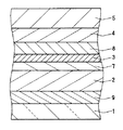
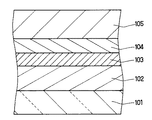
従来の光学情報記録媒体の代表的な層構成例を図10に示す。基板101には例えばポリカーボネート、ポリメチルメタクリレート(以下PMMA)等の樹脂またはガラス等が用いられ、レーザー光線を導くための案内溝が施されている。保護層102,104については後述する。記録層103は光学特性の異なる状態を有し、この状態間を可逆的に変化し得る物質からなる。書き換え型の相変化形光記録材料の場合、記録層103の材料としては、TeもしくはSeを含むいわゆるカルコゲナイド系材料またはSbを含む材料、例えばTe−Sb−Ge、Te−Sn−Ge、Te−Sb−Ge−Se、Te−Sn−Ge−Au、Ag−In−Sb−Te、In−Sb−Se、In−Te−Se等を主成分とする材料を用いることができる。反射層105は、例えばAu、Al、Cr等の金属、又はこれら金属の合金よりなり、放熱効果や記録薄膜の効果的な光吸収を目的として設けられるが、必須の層ではない。また、図中では省略したが、光学情報記録媒体の酸化、腐食やほこり等の付着の防止を目的として、反射層105の上にオーバーコート層を設けた構成、或いは紫外線硬化樹脂を接着剤として用い、ダミー基板を貼り合わせた構成を採用してもよい。
【0005】
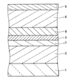
また、例えば図11に示すように、基板101と記録層103との間の保護層を、保護層102と保護層106とに2層化した記録媒体も提案されている。例えば特開平5−217211号公報では、Agを含有する記録層の保護層として、記録層に接する第1の保護層にSiNもしくはAlNの窒化物、またはSiCの炭化物を設け、その外側の第2の保護層にZnSまたはZnSを含有する複合化合物を設けた構成が開示されている。第1の保護層は、第2の保護層の構成原子のSと記録層の構成原子のAgとの反応を抑制するために形成されている。別の例として例えば特開平6−195747号公報では、図11に示すように記録層103と基板101との間の保護層を2層化し、記録層103に接する第1の保護層106をSi3N4、基板101と接する第2の保護層102にZnS−SiO2を適用する構成が開示されている。
【0006】
保護層102、104、106は記録層103の材料の酸化、蒸発や変形を防止するといった記録層103の保護機能を担う。また、保護層102、104、106の膜厚を調節することによって、光学情報記録媒体の吸収率や、記録部と消去部の間の反射率差を調節でき、媒体の光学特性の調節機能も担っている。保護層102、104、106を構成する材料の条件としては、上記目的を満たすばかりでなく、記録材料や基板101との接着性が良いこと、保護層102、104、106自身がクラックを生じない耐候性の良い膜であることが要求される。また、これらの保護層102、104、106が記録層103に接して用いられる場合は、記録材料の光学的変化を損なわない材料でなければならない。保護層102、104、106の材料としては、ZnS等の硫化物、SiO2、Ta2O5、Al2O3等の酸化物、GeN、Si3N4、Al3N4等の窒化物、GeON、SiON、AlON等の窒酸化物、その他炭化物、弗化物等の誘電体、或いはこれらの適当な組み合わせが提案されている。
【0007】
従来より、記録の書き換えを行った場合、書き換え後のマーク位置が微妙にずれ、いわゆるオーバーライト歪み(記録マークの歪み)が生じるという現象が知られていた。この歪みが生じる原因は、書き換え前の状態がアモルファスであるか、結晶であるかによって、レーザー照射時の温度上昇の様子が異なり、書き換え後のマークが所定の長さよりずれることにある。これを解決するために、アモルファス部の吸収率をAa、結晶部の吸収率をAcとしたとき、Ac/Aaを1より大きいある一定の範囲に保つという、いわゆる吸収補正が可能な構成をとると、マーク部分での温度上昇が均一となり、書き換えのマーク歪みが生じ難くなる。
【0008】
例えば、特開平7−78354号公報には、基板上に順に金属層、保護層、記録層、反射層を有し、記録後の反射率を記録前の反射率より大きくする提案がなされている。
【0009】
また、特開平7−105574号公報には、基板上にTiからなる光吸収層を設けた構成で、記録層での結晶状態の光吸収率を、非晶質状態での吸収率よりも大きくし、記録マークの位置ずれを生じ難くする提案が開示されている。
【0010】
【発明が解決しようとする課題】
特に高速で記録の書き換えを行うと、上述のオーバーライト歪みが生じ易くなってしまう。しかし、これを解決するために、単に、Ac/Aa>1としたのでは、消去率が十分に得られないという課題がある。その一方、消去率を上げるために結晶化速度が速い記録層組成を用いると、記録信号の十分な信頼性を得ることが困難であった。
【0011】
そこで、本発明は、上記課題を解決し、オーバーライト歪みを抑制しながら、かつ速い結晶化速度を得るべく高速で情報を記録できる光学情報記録媒体とその記録再生方法を提供することを目的とする。また、結晶化速度が速い場合であっても、記録信号の信頼性が高い光学情報記録媒体とその記録再生方法を提供することを目的とする。
【0012】
【課題を解決するための手段】
上記目的を達成するため、本発明の光学情報記録媒体は、結晶状態とアモルファス状態との間を可逆的に変化する記録層を含み、前記記録層に所定波長のレーザ光を入射することにより、前記記録層を前記結晶状態および前記アモルファス状態から選ばれるいずれか一方から他方へと変化させる光学情報記録媒体であって、前記記録層が前記結晶状態であるときの前記記録層における前記レーザ光の吸収率Acが、前記記録層が前記アモルファス状態であるときの前記記録層における前記レーザ光の吸収率Aaよりも大きく、前記記録層の両側に接して、前記記録層の前記アモルファス状態から前記結晶状態への変化を促進する結晶化促進層が設けられており、前記光学上方記録媒体は、いずれかの層に光吸収補正層をさらに含み、前記レーザ光の前記所定波長における前記光吸収補正層の屈折率が2よりも小さく、前記レーザ光の前記所定波長における前記光吸収補正層の吸収係数が2よりも大きいことを特徴とする。
【0013】
これにより、高速条件下での記録の書き換えにおいても高い消去率が得られる媒体を提供することができる。
【0014】
また、上記目的を達成するため、本発明の光学情報の記録再生方法は、結晶状態とアモルファス状態との間を可逆的に変化する記録層を含み、前記記録層に所定波長のレーザ光を入射させることにより、前記記録層が前記結晶状態および前記アモルファス状態から選ばれるいずれか一方から他方へと変化し、
前記記録層が前記結晶状態であるときの前記レーザ光の前記記録層における吸収率Acが、前記記録層が前記アモルファス状態であるときの前記レーザ光の前記記録層における吸収率Aaよりも大きく、
前記記録層の両側に接して結晶化促進層を設けた光学情報記録媒体を用いた光学情報の記録再生方法であって、
光学系により微小スポットに絞り込んだレーザー光の照射により前記記録層のうちの局所的な一部分が結晶状態からアモルファス状態へと可逆的に変化し得るアモルファス状態生成パワーレベルをP1、前記レーザー光の照射により前記記録層の局所的な一部がアモルファス状態から結晶状態へと可逆的に変化し得る結晶状態生成パワーレベルをP2、前記P1および前記P2のいずれのパワーレベルよりも低く、前記レーザー光の照射によって前記記録層の光学的状態が影響を受けず、かつその照射によって光学情報の再生のために十分な反射が得られる再生パワーレベルをP3としたとき、
前記レーザー光のパワーレベルを前記P1と前記P2との間で変調させることにより光学情報の記録、消去または上書きを行い、前記P3のパワーレベルの前記レーザー光を照射することにより光学情報の再生を行うことを特徴とする。
【0015】
これにより、オーバーライト歪みを抑制しながら、情報信号の高速度での記録、再生が可能となる。
【0016】
【発明の実施の形態】
本発明に関する光学情報記録媒体の層構成の一例を図1〜図3に示す。図1に示す光学情報記録媒体は、基板1上に、光吸収補正層9、保護層2、第1の結晶化促進層7、記録層3、第2の結晶化促進層8、反射層5がこの順に積層された構成を有する。また、図2に示す光学情報記録媒体は、基板1上に、保護層2、第1の結晶化促進層7、記録層3、第2の結晶化促進層8、光吸収補正層9がこの順に積層された構成を有する。また、図3に示す光学情報記録媒体は、基板1上に、保護層2、第1の結晶化促進層7、記録層3、第2の結晶化促進層8、光吸収補正層9、反射層5がこの順に積層された構成を有する。
【0017】
但し、本発明は上記構成に限定されるものではない。例えば、図1において、基板1と光吸収補正層9との間に層を設ける構成、第2の結晶化促進層8と反射層5との間に別の層を設ける構成、保護層2をすべて第1の結晶化促進層7で置き換えた構成、反射層のない構成等種々の構成に適用することが可能である。図2および図3においても種々の構成を適用できる。例えば、図2または図3において、第2の結晶化促進層8と光吸収補正層9との間に第2の保護層を設けてもよい。
【0018】
基板1の材料には、ポリカーボネート、PMMA等の樹脂、またはガラス等が用いられ、レーザー光線を導くための案内溝が施されていることが好ましい。
【0019】
保護層2は、記録層3での効果的な光吸収を可能にする光学特性の調節を主な目的として設けられる。保護層2の材料としては、ZnS等の硫化物、SiO2、Ta2O5、Al2O3等の酸化物、GeN(但し、価数は任意)、Si3N4、Al3N4等の窒化物、GeON、SiON、AlON(但し、価数は任意)等の窒酸化物、その他炭化物、フッ化物等の記録再生消去に適用するレーザー光を透過するいわゆる誘電体、或いはこれらの適当な組み合わせ(例えばZnS−SiO2等)など、上記目的が達成可能な材料を用いる。
【0020】
第1および第2の結晶化促進層7、8は、記録層3の酸化、腐食、変形等の防止といった記録層保護の役割を担うとともに、以下に述べるように、記録層3に接して設けられるがゆえの、重要な2つの役割を担っている。
【0021】
1つ目は、記録層3と保護層2との間の原子拡散または原子移動、特に保護層2中に硫黄または硫化物が含まれる場合、これらの成分が記録層3へと拡散または移動することを防止するという役割である。この保護層2及び/又は記録層3の構成原子が他方の層へ原子拡散または原子移動(以下、「原子拡散」と称する)を防止することにより、媒体の繰り返し特性は飛躍的に向上する。原子拡散の防止という点からいえば、結晶化促進層7、8を設ける位置は、記録層3のいずれか一方であっても両側であってもよいが、より効果的に防止するためには、両側に設けることが好ましい。原子拡散の防止については、記録層3界面での熱の負荷が大きくかかる側、すなわち、記録または消去時における記録層3界面での温度上昇が高い方(多くの場合、これはレーザー光入射側となる)の界面に設けた場合(すなわち、第1の結晶化促進層7)、非常に顕著にその効果が現れる。なお、結晶化促進層7、8中に含有される成分が、情報の繰り返し記録に伴い記録層3に拡散または移動する場合もありうる。このような観点からは、記録層3の光学変化を妨げにくい材料(例えば、Ge、Cr、Si、Al)を結晶化促進層7、8の構成材料として用いることが好ましい。
【0022】
結晶化促進層7、8の2つ目の重要な役割は、記録層3に接して設けた場合、記録マーク(アモルファス部分)の熱的安定性を損なわずに、記録材料の結晶化を促進する効果を発揮することである。これにより、さらなる高速消去が可能となる。この効果は特に、記録層3の温度上昇の低い側の界面、すなわち、多くの場合でレーザー入射側と反対側の記録層3界面に設けた場合(すなわち、第2の結晶化促進層8)に顕著となる場合が多い。
【0023】
図4に示したように、記録の書き換えを行う場合、書き換え前後での記録マーク(アモルファス部分)が重なっていると、記録層では、アモルファス状態から結晶状態への移行(領域21)、結晶状態からアモルファス状態への移行(領域23)のみならず、アモルファス状態からアモルファス状態への移行(領域22)が生じる。
【0024】
このとき、オーバーライト歪みは、主として、領域21と領域22との境界24で生じる。この理由を以下に述べる。領域22では書き換えの前後がともにアモルファス状態であるため、結晶状態からアモルファス状態へと相変化する領域23に比べて、結晶が溶融するための潜熱を必要としない。このため、書き換えの際に、領域22と領域23とに同量の熱量が与えられた場合は、領域22で余分な熱量が生じる。この余剰熱量は領域21をアモルファス化してしまい、このため、境界24が領域21の方向へとずれることになる。
【0025】
ここで、Ac/Aa>1とすると、書き換え前の領域22での光吸収が、領域23でのそれよりも少なくなるため、境界24の位置のずれを少なくすることができる。しかし、Aaが相対的に小さくなるため、領域21が結晶化するための十分な光吸収ができず、結晶化が困難になってしまう。このため、境界24の位置のずれは生じにくくなるものの、領域21の結晶化が不十分となることにより、オーバーライト後で高い消去率を得ることが困難であった。
【0026】
上記課題を解決するための案として、少ない光吸収でも結晶化が可能である、結晶化速度の速い記録層組成を用いることが考えられる。この場合は、領域21が結晶化し易くなり、より高い消去率が得られるようになる。しかし、結晶化を速めている分、アモルファスの熱的安定性が損なわれるため、記録マークが長時間の保存に耐えることが困難になるという新たな課題が生じてしまう。
【0027】
そこで、本発明では、結晶化促進層を設けることにより、少ない光吸収でも十分にアモルファス状態から結晶状態へと変化しうるようにした。したがって、結晶化速度が比較的遅い記録層組成を用いてアモルファス部分の熱的安定性を十分に得た場合でも、結晶化を速くすることが可能となり、高い消去率を得ることができる。
【0028】
また、高速での良好な書き換え特性と、良好な繰り返し特性との両方を兼ね備えるため、本発明では、結晶化促進層を記録層3の両側に設けることとした。
【0029】
結晶化促進層7、8に適用する材料は、上記の2つの役割を果たす材料であればよいが、窒化物、窒酸化物、酸化物または炭化物のいずれかを主成分とする材料であれば好ましい。例えば、窒化物としては、GeN、CrN、SiN、AlN、NbN、MoN、FeN、TiN、ZrN(但し、価数は任意。以下同じ)等、窒酸化物としては、GeON、CrON、SiON、AlON、NbON、MoON(但し、価数は任意。以下同じ)等、酸化物としては、SiO2、Ta2O5、Al2O3等、炭化物としてはCrC、SiC、AlC、TiC、TaC、ZrC(但し、価数は任意。以下同じ)等を用いることができ、或いは、これらの適当な混合物としてもよい。いずれにせよ、結晶化促進層7、8の材料としては、記録層3と保護層2との構成原子の原子拡散を起こしにくい材料であるか、または仮に記録層3に拡散した場合でも記録層3の光学変化を妨げにくい材料であり、記録層3と接して設けた場合に、記録層3の結晶化を促進する材料が好ましい。
【0030】
結晶化促進層7、8を構成する材料として、GeおよびNを含む材料、具体的には例えば、GeN、GeON、GeXN、GeXON(但し、XはCr、Mo、Mn、Ni、CoおよびLaから選ばれる少なくとも1つの元素を含む材料)のうちの少なくとも1つを主成分とする材料を用いた場合に、特に優れた繰り返し特性及び耐候性を得ることができる。ただし、結晶化促進の効果は、GeN、GeON、GeXN、GeXONのいずれを用いてもほぼ同様に得られる。なお、物質XはGeN膜またはGeON膜の耐候性向上を主な目的として添加される物質である。上記6元素を含む材料の他にもY、Fe、Ti、Zr、Nb、Ta、Cu、Zn、Pd、Ag、Cd、Hf、Wを含む材料としてもよいが、上記の6元素(Cr、Mo、Mn、Ni、Co、La)のうちの少なくとも1元素を含む場合、より効果的に耐候性が向上する。
【0031】
また、結晶化促進層7、8を構成する材料としては、ZnS−SiO2を主成分とする材料を用いてもよい。特に、結晶化促進層7、8中でのZn含有量のS含有量に対する比((Zn含有量)/(S含有量))が1より大きい材料(以下、Znリッチと称す)、或いは、O含有量のSi含有量に対する比((O含有量)/(Si含有量))が2より大きい材料(以下、Oリッチと称す)を用いることが好ましい。Znリッチ組成またはOリッチ組成を有するZnS−SiO2層は、記録層3と接して設けられた場合に、記録層3の結晶化促進の効果があり、しかも保護層2と記録層3との原子拡散を抑制する効果を有するため、結晶化促進層7、8として適している。
【0032】
結晶化促進層7、8の膜厚は、原子拡散防止効果を確実にするために、その膜厚の下限は1nm以上(さらに5nm以上)であることが好ましい。また、結晶化促進層7、8は記録再生消去に必要なレーザービームが記録層3に透過すればよく、従ってその膜厚の上限は特に限定されるものではない。
【0033】
次に、記録層3の材料としては、光学特性が可逆的に変化する材料を用いる。相変化形記録媒体の場合、Sb系またはTe、Seを主成分とするカルコゲナイド系材料を用いることが好ましい。例えばTe−Sb−Ge、Te−Sn−Ge、Te−Sb−Ge−Se、Te−Sn−Ge−Au、Ag−In−Sb−Te、In−Sb−Se、In−Te−Se等を主成分とする材料が挙げられる。
【0034】
或いは、高密度化を図る場合、記録層組成をGe−Sb−Te3元組成図(図5)において、GeTe−Sb2Te3ライン上の組成(或いはライン上の組成にSbを適量添加した組成)のうちGeTeに近い側の組成を用いることが好ましい。従来、このような組成を用いると、記録の繰り返し特性が悪化するという新たな問題が生じていたが、結晶化促進層7、8を設けることで、上述の通りこれが回避され、比較的GeTe側の組成を用いても、書き換え記録の高速化と良好な繰り返し特性との両立が可能となる。
【0035】
また、記録層の組成としては、((GeTe)1-x(Sb2Te3)x)1-ySby(ただし、1/13≦x≦1/3、0≦y≦2/3)により示される組成が好ましい。この組成は、具体的には、図5に示す点A(Ge41.4Sb6.9Te51.7)、点B(Ge22.2Sb22.2Te55.6)、点C(Ge18.2Sb36.4Te45.5)、点D(Ge38.7Sb12.9Te48.4)で囲まれる範囲である。この範囲の組成を有する記録層は、従来の構成では、必ずしも高線速での使用が可能ではなかったが、本発明により、高線速での使用が可能になった範囲でもある。
【0036】
記録層3中にはAr、Kr等のスパッタガス成分やH、C、H2O等が不純物として含まれることがあり、また、種々の目的のために記録層3の主成分Ge−Sb−Te材料に他の物質を微量(例えば約10at%以下)添加する場合もあり得るが、これらの構成を本発明で排除するものではない。
【0037】
記録層3の膜厚は1nm以上25nm以下であることが好ましい。これは膜厚が1nm未満の場合には記録材料が層状になりにくいためであり、25nmを超える場合には記録層面内での熱拡散が大きくなるため、高密度で記録を行った際に隣接消去が生じ易くなるためである。
【0038】
反射層5は、Au、Ag、Cu、Al、Cr、Ni等の金属、或いは適宜選択された金属の合金より形成する。
【0039】
光吸収補正層9は、媒体でのアモルファス部の吸収率をAa、結晶部の吸収率をAcとしたとき、Ac/Aaを1より大きいある一定の範囲に保つという、いわゆる吸収補正を可能にするために設けられる層である。
【0040】
光吸収補正層9を形成することにより、Ac/Aa≦1である媒体においても、Ac/Aa>1とすることができる。光吸収補正層9の具体的な構成については後述する。
【0041】
Ac/Aa>1を実現する方法としてはいくつか挙げられる。まず、アモルファス状態の反射率Raが結晶状態の反射率Rcより高い構成とする方法が挙げられる。この場合、例えばアモルファス状態と結晶状態との間の反射率差|Ra−Rc|を大きくとった場合でも、Ac/Aaの値を大きくすることができる。このため、Ac/Aa値を大きい値とすることができる。すなわち、より高速の条件下での書き換えを行う場合でも、マーク歪みを抑制することが可能となる。
【0042】
また、アモルファス状態での反射率が結晶状態の反射率より低い場合でもAc/Aa>1を実現することができる。このような方法としては、媒体に透過を生じさせ、記録層がアモルファス状態であるときの媒体の透過率をTa、結晶状態での媒体の透過率をTcとしたとき、0<Tc<Taとする方法が挙げられる。
【0043】
また、別の方法として、記録層がアモルファス状態であるときの記録層以外の層における吸収率をA’a、記録層が結晶状態であるときの記録層以外の層におけるを吸収率A’cとしたとき、0<A’c<A’aとする方法が挙げられる。具体的には、媒体中に吸収を生じる層を設け、この層での光吸収が、記録層がアモルファス状態であるときAa2、結晶状態であるときAc2としたとき、0<Ac2<Aa2を満たす構成とすることが挙げられる。
【0044】
Rc<Raの反射率構成を持つ媒体は、既述のようにAc/Aa>1となる構成を設計しやすいという大きな利点がある。しかし、アモルファス部と結晶部の反射率の和が、Rc>Raの反射率構成を有する媒体に比べて概して大きくなるため、信号再生時のノイズが増加しやすいという不利な点もある。一方、Rc>Raの反射率構成の場合、このような欠点は生じにくいが、反射率差|Rc−Ra|を大きくしたい場合には比較的不利である。
【0045】
上記で述べた3つの構成、すなわち「Ra>Rcの構成」、「Ra<Rcかつ0<Tc<Taの構成」、「Ra<Rcかつ0<Ac2<Aa2の構成」の例をそれぞれ図1、図2、図3に示す。
【0046】
図1の構成における光吸収補正層9は、Ra>Rcを容易に可能とする役割をもっている。このときの光吸収補正層は、ある程度のレーザー光を反射、或いは吸収するが、残りは透過させなければならない。
【0047】
Ra>Rcを効果的に達成するためには、光吸収補正層9をなす材料の使用レーザー波長域での光学定数n−ikの屈折率n及び吸収係数kが、n<2かつk>2、或いは、n>2かつk<2を満たす範囲内であることが好ましい。ここで、n<2かつk>2を満たす材料としては、Au、AgおよびCuから選ばれる少なくとも1種を含む材料が挙げられる。あるいは、この材料に加えて、Al、CrまたはNiを含む材料を用いてもよい。一方、n>2かつk<2を満たす材料としては、Si、Ge、Cr、S、SeおよびTeから選ばれる少なくとも1種を含む材料が挙げられる。
【0048】
さらに具体的には、膜厚の薄いAu、Ag、Cu等の金属、或いはSi、Ge、Teを主成分とする半導体または誘電体、或いはAuCr、CuNi、SiCr等のこれらの適当な混合物を用いることができる。金属としては、Au、AgまたはCuを主成分とする金属を用いることが好ましい。この場合、熱伝導率等を調整するために、Al、Cr、Ni等の金属を、好ましくは30%以下の範囲で添加してもよい。
【0049】
なお、図1に示した構成の場合、光吸収補正層9は、記録層3と基板1との間のいずれかの場所に設けることが好ましい。ただし、記録マーク間の熱干渉を抑制し、クロス消去特性を良好に保つためには、光吸収補正層9が、記録層3からある程度離れた位置、例えば基板1のすぐ上の位置等に設けることがより好ましい。
【0050】
図1に示した媒体の好ましい構成例を以下に例示する。光吸収補正層9は、膜厚5〜30nmのn<2かつk>2を満たす材料、または膜厚5〜30nmのn>2かつk<2を満たす材料である。保護層2は、膜厚60〜120nmのZnS−SiO2である。第1の結晶化促進層7は、膜厚1〜40nmのSiC−SiNである。あるいは、結晶化促進層7として、膜厚1〜40nmのAlCrN、SiCrN、GeCrNまたはGeNiNを用いてもよい。記録層3は、膜厚5〜25nmの上記に例示した好ましい範囲の組成を有するGeSbTeである。第2の結晶化促進層8は、膜厚10〜80nmのSiC−SiNである。あるいは、結晶化促進層8として、AlCrN、SiCrN、GeCrNまたはGeNiNを用いてもよい。反射層5は、膜厚20〜120nmのAuまたはAgを主成分とする材料である。
【0051】
図2の構成での光吸収補正層9は、その膜厚を薄くすることにより透過を生じさせた層であり、0<Tc<Taを実現している。
【0052】
0<Tc<Taを効果的に達成するためには、光吸収補正層9をなす材料の使用レーザー波長域での光学定数n−ikの屈折率n及び吸収係数kが、n<3かつk<6を満たす範囲内であることが好ましい。
【0053】
このような材料としては、Au、Ag、Cu、Al、Cr、Ni、SiおよびGeから選ばれる少なくとも1種を含む材料が挙げられる。具体的には、上記と同様に、膜厚の薄いAu、Ag、Cu、Al、Cr、Ni等の金属、或いはSi、Ge等を主成分とする半導体または誘電体(特に記録再生消去に適用するレーザー光に対して所定の透過率を有するような膜厚を備えた金属、半導体または誘電体)、或いはこれらの適当な混合物を用いることができる。
【0054】
さらに具体的には、Au、AgもしくはCuを主成分とする金属、またはGeもしくはSiを主成分とする半導体または誘電体を用いることが好ましい。
【0055】
光吸収補正層9の膜厚は、材料に応じて定められる上限値以下とすることが好ましい。例えばAuを用いた場合、その膜厚は約20nmより薄くすることが好ましい。
【0056】
なお、図2に示した構成の場合、光吸収補正層9は、レーザ光入射の方向と反対側の最も上の位置に設けることが好ましい。
【0057】
図2に示した媒体の好ましい構成例を以下に例示する。保護層2は、膜厚100〜160nmのZnS−SiO2である。第1の結晶化促進層7は、膜厚1〜40nmのSiC−SiNである。あるいは、結晶化促進層7として、膜厚1〜40nmのAlCrN、SiCrN、GeCrNまたはGeNiNを用いてもよい。記録層3は、膜厚5〜25nmの上記に例示した好ましい範囲の組成を有するGeSbTeである。第2の結晶化促進層8は、膜厚60〜140nmのSiC−SiNである。あるいは、結晶化促進層8として、AlCrN、SiCrN、GeCrNまたはGeNiNを用いてもよい。光吸収補正層9は、膜厚1〜20nmのn<3かつk<6を満たす材料である。
【0058】
また、図2に示した構成では、放熱効果が低下するおそれがあるため、図2の光吸収補正層9上に、さらにAlN、TaN、InO、SnO(ただし、価数は問わない)等の透明誘電体層を積層してもよい。
【0059】
図3の構成での光吸収補正層9は、この層で光吸収を行うことによりAc/Aa>1を可能とする層であり、使用するレーザー波長域において、適度な光吸収を有する層を設ける。この光吸収補正層は、記録層がアモルファス状態であるときの吸収率Aa2が、記録層が結晶状態であるときの吸収率Ac2よりも大きい層(0<Ac2<Aa2)として形成される。
【0060】
0<Ac2<Aa2を効果的に達成するためには、光吸収補正層9をなす材料の使用レーザー波長域での光学定数n−ikの屈折率n及び吸収係数kが、n>2かつk>2を満たす範囲内であることが好ましい。
【0061】
このような材料としては、Ge、Si、Cr、Se、SおよびTeから選ばれる少なくとも1種を含む材料が挙げられる。具体的には、Ge、Si、Cr、Se、SおよびTeから選ばれる少なくとも1種を主成分とする半導体または誘電体が好ましい。このような材料としては、例えば、GeCr、SiTa、SiW、PbS、PbTe等が挙げられる。
【0062】
なお、図3に示した構成の場合、光吸収補正層9は、反射層5の手前の位置にに設けることが好ましい。
【0063】
図3に示した媒体の好ましい構成例を以下に例示する。保護層2は、膜厚100〜160nmのZnS−SiO2である。第1の結晶化促進層7は、膜厚1〜40nmのSiC−SiNである。あるいは、結晶化促進層7として、膜厚1〜40nmのAlCrN、SiCrN、GeCrNまたはGeNiNを用いてもよい。記録層3は、膜厚5〜25nmの上記に例示した好ましい範囲の組成を有するGeSbTeである。第2の結晶化促進層8は、膜厚10〜80nmのSiC−SiNである。あるいは、結晶化促進層8として、AlCrN、SiCrN、GeCrNまたはGeNiNを用いてもよい。光吸収補正層9は、膜厚5〜50nmのn>2かつk>2を満たす材料である。反射層5は、膜厚20〜120nmのAuまたはAgを主成分とする材料である。
【0064】
上記各構成例では、保護層を追加して設けてもよい。例えば、図1〜図3の構成例における保護層2を第1の保護層として、さらに第2の保護層4を追加した例を、図6〜図8に示す。図6に示した構成は、図1の構成例において、第2の結晶化促進層8と反射層5との間に第2の保護層4を形成した例である。図7に示した構成は、図2の構成例において、第2の結晶化促進層8と光吸収補正層9との間に第2の保護層4を形成した例である。図8に示した構成は、図3に示した構成例において、第2の結晶化促進層8と光吸収補正層9との間に第2の保護層4を形成した例である。
【0065】
次に、これらの光学情報記録媒体の製造方法について述べる。上記光学情報記録媒体を構成する多層膜を作製する方法としては、スパッタリング法、真空蒸着法、CVD法等のいわゆる気相堆積法が可能である。ここでは、一例として、図9に、スパッタリング法を用いるときの成膜装置の概略を示す。
【0066】
真空容器10には排気口16を通して真空ポンプ(図示省略)を接続してあり、真空容器内を高真空に保つことができるようになっている。ガス供給口15からは、一定流量の希ガス、窒素、酸素、またはこれらの混合ガスを供給することができるようになっている。図中11は基板であり、基板の自公転を行うための駆動装置12に取り付けられている。図中13はスパッタターゲットであり、陰極14に接続されている。陰極14は、図示は省略したが、スイッチを通して直流電源または高周波電源に接続されている。また、真空容器10を接地することにより、真空容器10及び基板11は陽極に保たれている。
【0067】
各層を成膜する際の成膜ガスとしては、希ガスを含むガスを用いる。希ガスにはAr、Kr等が単独または必要に応じて混合して用いられる。記録層3、及び保護層2の成膜ガスに、微量の窒素または酸素を混合することがあるが、これは、繰り返し記録時での記録層の物質移動を抑制する効果があるためである。なお、記録層3を成膜する際は、例えばGe−Sb−Teターゲットが用いられる。
【0068】
結晶化促進層7、8として窒化物を用いる場合、反応性スパッタリング法により成膜すると良好な膜質の膜が得られる。例えば、結晶化促進層としてGeCrNを用いる場合、GeCrまたはGeCrとNとを含む材料をターゲットとし、成膜ガスとして希ガスと窒素の混合ガスを用いる。或いはN2O、NO2、NO、N2等の窒素原子を含むガスや、これらの適当な組み合わせの混合ガスと希ガスとの混合ガスを用いてもよい。また、膜が硬質である場合や膜応力が大きい場合等、必要に応じて微量の酸素を成膜ガス中に混合することにより、良好な膜質の層を得ることができる場合がある。
【0069】
次に、以上のようにして形成した光学情報記録媒体の記録再生消去方法について述べる。信号の記録再生消去には、例えば、レーザー光源と、対物レンズを搭載した光ヘッドと、レーザー光を照射する位置を所定の位置へと導くための駆動装置、トラック方向及び膜面に垂直な方向の位置を制御するためのトラッキング制御装置及びフォーカシング制御装置と、レーザーパワーを変調するためのレーザー駆動装置、媒体を回転させるための回転制御装置とを用いる。
【0070】
信号の記録または消去は、まず媒体を回転制御装置を用いて回転させ、光学系によりレーザー光を微小スポットに絞りこんで、媒体へレーザー光を照射することにより行う。レーザーの照射により記録層のうちの局所的な一部分がアモルファス状態へと可逆的に変化しうるアモルファス状態生成パワーレベルをP1、同じくレーザーの照射により結晶状態へと可逆的に変化しうる結晶状態生成パワーレベルをP2とし(通常、P1>P2)、レーザーパワーをP1とP2の間で変調させることで記録マークを形成、或いは記録マークを消去し、情報の記録、消去、及び上書き記録を行った。ここではP1のパワーを照射する部分は、パルスの列で形成する、いわゆるマルチパルスとした。但し、マルチパルスを用いないパルスで構成してもよいが、本発明の書き換えの高速化及び繰り返し特性の向上を達成するためには、マルチパルスを適用することが好ましい。
【0071】
また、前記P1、P2のいずれのパワーレベルよりも低く、そのパワーレベルでのレーザー照射によって記録マークの光学的な状態が影響を受けず、レーザー照射によって媒体から記録マークの再生のために十分な反射率が得られるパワーレベルを再生パワーレベルP3とし、P3のパワーのレーザービームを照射することにより得られる媒体からの信号を検出器で読みとり、情報信号の再生を行った。なお、レーザ光の波長は、780nm以下の範囲が好ましい。
【0072】
また、光学情報記録媒体に記録再生する際のレーザビームの走査線速度は4m/s以上であることが好ましい。本発明においては、高速消去特性および繰り返し特性が向上し、より高い転送レートが得られる光学情報記録媒体が可能になるため、レーザビームの走査線速度をより大きくしたほうが本発明の特徴を顕著に発揮することができる。レーザビームの走査線速度は8m/s以上であることがより好ましい。
【0073】
ただし、非常に高密度での記録が可能になった場合は、線速度をさほど速くしなくとも高い転送レートが得られる。例えば、青色波長での記録再生を行う場合は、赤色波長での記録再生と比較して、非常に高密度での記録が可能となるため、同じ距離を再生した場合に得られる情報量が大きくなり、転送レートが高くなる。このような場合は、必ずしも8m/s以上の線速度を適用する必要はない。
【0074】
【実施例】
本発明の実施の一例を以下に示すが、本発明は以下の実施例により制限されるものではない。
【0075】
まず、図1と同様の構成で、基板1を厚さ0.6mm、直径120mmのディスク状ポリカーボネート樹脂、保護層2をZnSにSiO2を20mol%混合した材料、記録層3をGe21Sb25Te54、結晶化促進層7、8をGeCrN、光吸収補正層9をAuとした場合の記録媒体を(1)とする。なお、記録媒体(1)の各層の膜厚は、記録層3を12nm、保護層2を80nm、結晶化促進層7、8をそれぞれ10nm、50nm、反射層5を40nm、光吸収補正層9を10nmとした。
【0076】
比較例として、
記録媒体(1)における結晶化促進層7、8のそれぞれの膜厚10nm及び50nmはそのままで、保護層2と同じ材料で置き換えた他は記録媒体(1)と同様の構成を有する構成(すなわち、記録層3を保護層と同じ材料の層で挟持し、基板1と保護層2との間に光吸収補正層9を備えた構成)を記録媒体(2)とし、
記録媒体(1)における光吸収補正層9の膜厚10nmはそのままにし、保護層2と同じ材料で置き換えた他は記録媒体(1)と同様の構成を有する構成(すなわち、記録層3を結晶化促進層7及び8で挟持し、結晶化促進層7と基板1との間は保護層2のみを備えた構成)を記録媒体(3)とし、
記録媒体(1)における結晶化促進層8のみ膜厚50nmはそのままで、保護層2と同じ材料で置き換えた構成(すなわち、記録層3を結晶化促進層7と保護層と同じ材料の層とで挟持した構成)を記録媒体(4)とし、
記録媒体(4)で、さらに光吸収補正層9の膜厚10nmはそのままにし、保護層2と同じ材料で置き換えた構成(すなわち、記録層3を結晶化促進層7と保護層と同じ材料の層で挟持し、結晶化促進層7と基板との間を保護層2のみとした構成)を記録媒体(5)とし、
記録媒体(1)における結晶化促進層7のみ膜厚10nmはそのままにし、保護層2と同じ材料で置き換えた構成(すなわち、記録層3を保護層と同じ材料の層と結晶化促進層8とで挟持した構成)を記録媒体(6)とし、
記録媒体(6)で、さらに光吸収補正層9の膜厚を10nmはそのままにし、保護層2と同じ材料で置き換えた構成(すなわち、記録層3を保護層2と結晶化促進層8とで挟持し、記録層3と基板1との間を保護層2のみとした構成)を記録媒体(7)とした。
【0077】
記録層3及び保護層2を成膜する際は、Arに窒素を2.5%混合したガスを、全圧がそれぞれ1.0mTorr、0.5mTorrとなるように一定の流量で供給し、陰極にそれぞれDC1.27W/cm2、RF5.10W/cm2のパワーを投入して行った。反射層5を成膜する際は、Arガスを全圧3.0mTorrになるように供給し、DC4.45W/cm2のパワーを投入して行った。
【0078】
結晶化促進層7、8(GeCrN層)を成膜する際はターゲット材料をGeCrとし、GeCrN膜中に含有されるCr含有量の、Ge含有量とCr含有量の和に対する比率が20%となるようにした。スパッタガスはArと窒素との混合ガス、スパッタガス圧は10mTorr、スパッタガス中の窒素分圧は40%、スパッタパワー密度は6.37W/cm2で全て共通とした。
【0079】
以上により作製した記録媒体(1)〜(7)を用いて、光学情報の記録試験を実施した。
【0080】
記録の信号方式はEFM変調方式とし、用いたレーザー光の波長は650nm、対物レンズの開口数は0.60である。最短ビット長は0.28μm、即ち最短マーク長は0.41μm、ディスク回転速度は線速6m/s、及び12m/sで測定を行った。トラックピッチは1.20μm、即ち0.60μmごとに溝部とランド部が交互に形成される基板を用いた。
【0081】
特性の評価は、高線速でのオーバーライト消去率、及び記録の繰り返し特性について行った。
【0082】
高速消去特性の評価は、EFM信号方式での3T長さのマークを設定レーザーパワーで記録した後、11T長さのマークでオーバーライトしたときの消去率を測定することにより行った。オーバーライト消去率が30dB以上得られたものを○、30dBに満たなかったものを×として示した。
【0083】
記録の繰り返し特性は、EFM信号方式により最短マーク長が0.41μmとなる場合について3Tから11Tの長さのランダムマークを溝部に記録し、マークの前端間及び後端間のジッター値をウィンドウ幅Tで割った値(以下ジッター値)の、繰り返し記録後での増加分を評価することにより行った。10万回の繰り返し記録後で、10回記録時のジッター値と比較して、前端間、後端間ジッター値の増加分の平均が3%以下であるものを○、3%より大きかったものを×として示した。(1)〜(7)の媒体を評価した結果を(表1)に示す。
【0084】
(表1)

(表1)の結果より、結晶化促進層を記録層の上下に有しない記録媒体(2)、結晶化促進層を記録層の反射層側にのみ有する記録媒体(6)及び(7)では繰り返し特性が悪く、結晶化促進層を記録層の上下に有する構成、または結晶化促進層を記録層の基板側にのみ有する構成では良好な繰り返し特性が得られている。
【0086】
また、光吸収補正層9を有する記録媒体(1)、(2)、(4)及び(6)の内、記録層3の反射層5側の結晶化促進層8を有しない記録媒体(2)及び(4)では12m/sの高線速におけるオーバーライト消去率が劣り、記録層3の反射層5側にのみ結晶化促進層8を備えた記録媒体(6)では12m/sの高線速におけるオーバーライト消去率は良好ではあるが、繰り返し特性に劣る。
【0087】
さらに、記録層3の上下に結晶化促進層7、8を備えるが光吸収補正層9を有しない記録媒体(3)、及び記録層3の基板1側にのみ結晶化促進層7を備えるが光吸収補正層9を有しない記録媒体(5)では、12m/sの高線速側ではオーバーライト消去率が落ちている。
【0088】
結局、記録層3の上下に結晶化促進層7、8と光吸収補正層9とをともに有する本発明の記録媒体(1)では、高速消去が可能となり、繰り返し特性も良好であることがわかる。
【0089】
次に、図2と同様の構成で各層の膜厚は、保護層2を110nm、結晶化促進層7、8をそれぞれ10nm、120nm、記録層3を8nm、光吸収補正層9を10nmとし、各層の材料及び製法を記録媒体(1)と同様にした記録媒体を(8)とする。
【0090】
比較例として、
記録媒体(8)における結晶化促進層7、8のそれぞれの膜厚10nm及び120nmはそのままで、適用する材料を保護層2と同じ材料で置き換えた構成(すなわち、記録層3を保護層と同じ材料の層で挟持した構成)を記録媒体(9)、
記録媒体(8)における光吸収補正層9を50nmの上記反射層5で置き換えた構成(すなわち、記録層3を結晶化促進層7、8で挟持し、結晶化促進層8を記録層3と反射層5とで挟持した構成)を記録媒体(10)とする。
【0091】
さらに、図3と同様の構成で各層の膜厚は、保護層2を130nm、結晶化促進層7、8をそれぞれ10nm、40nm、記録層3を12nm、反射層5を40nm、光吸収補正層9を30nmのSiWとし、光吸収層以外の各層に用いる材料を記録媒体(1)と同様にした記録媒体を(11)とした。
【0092】
比較例として、
媒体(11)における結晶化促進層7、8のそれぞれの膜厚10nm及び40nmはそのままで、適用する材料を保護層2と同じ材料で置き換えた構成(すなわち、記録層3を保護層と同じ材料の層で挟持した構成)を記録媒体(12)、媒体(11)における光吸収補正層9の膜厚40nmはそのままで、用いる材料を保護層2と同じ材料で置き換えた構成(すなわち、結晶化促進層8と反射層5との間に保護層と同じ材料の層を挟持した構成)を記録媒体(13)とする。
【0093】
以上の媒体(8)〜(13)について特性評価を行った結果を(表2)に示す。(表2)からも、本発明の記録媒体(8)及び(11)が高速消去特性、良好な繰り返しの特性が得られることがわかる。
【0094】
(表2)
この結果は、図1の構成における傾向と同様であることから、図2または図3に示した層構成においても、記録層を介して一対の結晶化促進層を密着させると共に、光吸収補正層を形成してAc>Aaとした構成により、線速に依らず繰り返し特性及びオーバーライト消去率に優れた光情報記録媒体が提供できることが確認された。
【0096】
別の実施例として、媒体(1)と同様の層構成、材料を有し、記録層の組成のみ、Ge30.1Sb17.3Te52.6とした媒体を記録媒体(14)とする。
【0097】
比較例として、記録層の組成のみをGe14.3Sb28.6Te57.1とした点を除いては媒体(14)と全く同じ構成、材料を有する媒体を記録媒体(15)とする。
【0098】
別の比較例として、媒体(1)と同様の層構成を有するが、結晶化促進層7,8をすべて保護層の材料で置き換え、記録層の組成をGe30.1Sb17.3Te52.6およびGe14.3Sb28.6Te57.1とした媒体を、それぞれ記録媒体(16)、記録媒体(17)とする。
【0099】
これら媒体の評価を、記録の繰り返し特性、高線速でのオーバーライト消去率および耐環境試験特性について行った。繰り返し特性および高線速でのオーバーライト特性の評価基準については、既述の方法と同様とした。
【0100】
耐環境試験の評価は、以下の方法で行った。まず、オーバーライト特性の評価時と同じ条件を用いて、線速12m/sで3Tの長さのマークを記録し、このときの3T信号の前端および後端間のジッター値(記録マークの前端間および後端間のずれ量をウィンドウ幅で割った値)を測定した。次に媒体を90℃、相対湿度25%の高温条件に保持することにより、加速試験を行った。この後、記録したマークのジッター値を再度測定し、加速試験前に比べて加速試験後のジッター値の増加分が、前端間、後端間のいずれも2%以下である場合を○、前端間、後端間のジッター値のいずれかが2%以上増加していた場合を×とする。
【0101】
表3に、媒体(14)〜(17)を評価した結果を示す。また、既述の媒体(1)について、同様の耐環境試験を行った結果も併せて示す。
【0102】
(表3)
表3によると、Ge量が比較的少なく、かつGeTe−Sb2Te3で結ばれるライン上の組成である、Ge14.3Sb28.6Te57.1の組成を用いている、媒体(15)および媒体(17)は、オーバーライト消去率は良好であるものの、十分な耐環境試験特性が得られない。これに対して、媒体(1)、媒体(14)および媒体(16)の組成を用いた場合、アモルファスが熱的に安定するため、十分な耐環境試験特性を得ることができる。
【0104】
また、媒体(16)では、結晶化促進層を有しないため、繰り返し特性および高線速での消去率が良好ではないが、結晶化促進層を両側に有し、また吸収補正層9も有する、媒体(1)および媒体(14)では、繰り返し特性、高線速での消去率および耐環境試験特性のすべてにおいて、良好な特性を示すことが可能となる。
【0105】
表3の結果より、従来、高線速条件で高い消去率が得られなかった記録層組成であっても、記録層の両側に結晶化促進層を設けるとともに、光吸収補正層を形成してAc>Aaとした構成を用いることにより、記録の繰り返し特性およびオーバーライト消去率に優れた光学情報記録媒体を提供できることが確認できた。
【0106】
さらに別の実施例として、図6〜図8に示した構成と同様となるように、記録媒体を作製した。
【0107】
図6と同様の構成で、基板1を厚さ0.6mm、直径120mmのディスク状ポリカーボネート樹脂、保護層2、4をZnSにSiO2を20mol%混合した材料、記録層3をGe30.0Sb18.0Te52.0、反射層5をAlCr、結晶化促進層7、8をSiCrN、光吸収補正層9をAgPdとした場合の媒体を記録媒体(18)とする。なお、記録媒体(18)の各層の膜厚は、光吸収補正層9を5nm、保護層2を80nm、結晶化促進層7を5nm、記録層3を9nm、結晶化促進層8を5nm、保護層4を40nm、反射層5を80nmとした。
【0108】
また、図7と同様の構成で、記録層3をGe29.4Sb19.1Te51.5、結晶化促進層7、8をAlNiN、光吸収補正層9をAuPdとした点を除いては、記録媒体(18)と同じ材料を用いて構成した媒体を、記録媒体(19)とする。なお、記録媒体(19)の各層の膜厚は、保護層2を120nm、結晶化促進層7を5nm、記録層3を10nm、結晶化促進層8を5nm、保護層4を120nm、光吸収補正層9を10nmとした。
【0109】
また、図8と同様の構成で、結晶化促進層7、8をGeCrN、光吸収補正層9をSiTa、反射層5をAlとした点を除いては、記録媒体(18)と同じ材料を用いて構成した媒体を、記録媒体(20)とする。なお、記録媒体(20)の各層の膜厚は、保護層2を130nm、結晶化促進層7を2nm、記録層3を9nm、結晶化促進層8を2nm、保護層4を40nm、光吸収補正層9を30nm、反射層5を80nmとした。
【0110】
これら媒体(18)〜(20)の評価を、記録の繰り返し特性、高線速でのオーバーライト特性、耐環境試験特性について行った。評価の方法は、媒体(14)〜(17)と同様とした。その結果、媒体(18)〜(20)についての評価結果は、いずれの項目についても○に相当するものであった。
【0111】
【発明の効果】
以上述べたように、光学特性が可逆的に変化する記録層の両側に接して結晶化促進層を設け、Ac>Aaとすることにより、信号の書き換えの高速化が可能であり、記録マークの熱的安定性、記録の繰り返し特性にも優れた光情報記録媒体が得られ、当該光情報記録媒体の性能を遺憾なく発揮できる記録再生消去方法とが得られる効果がある。
【図面の簡単な説明】
【図1】 本発明における層構成の例を示す断面図
【図2】 本発明における層構成の別の例を示す断面図
【図3】 本発明における層構成のさらに別の例を示す断面図
【図4】 オーバーライト歪みを説明するための模式図
【図5】 記録層の好ましい組成範囲を示すための3元組成図
【図6】 本発明における層構成の別の例を示す断面図
【図7】 本発明における層構成のまた別の例を示す断面図
【図8】 本発明における層構成のさらに別の例を示す断面図
【図9】 成膜装置の一例を模式的に示す図
【図10】 従来の層構成の一例を示す図
【図11】 従来の層構成の他の例を示す図
【符号の説明】
1 基板
2 (第1の)保護層
3 記録層
4 (第2の)保護層
5 反射層
7 (第1の)結晶化促進層
8 (第2の)結晶化促進層
9 光吸収補正層
10 真空容器
11 基板
12 基板駆動装置
13 ターゲット
14 陰極
15 ガス供給口
16 排気口[0001]
BACKGROUND OF THE INVENTION
The present invention relates to a phase change type optical recording information medium capable of recording / reproducing and rewriting information at high density and high speed using optical means such as laser beam irradiation, and a recording / reproducing method thereof. .
[0002]
[Prior art]
Magneto-optical recording media, phase change recording media, and the like are known as media capable of recording information in a large capacity and capable of being reproduced and rewritten at high speed. These high-capacity recording media with excellent portability will become increasingly demanded in the advanced information society in the future, and as the functions of applications and the performance of video information become higher, the capacity and speed will be further increased. Is desired.
[0003]
These optical recording media utilize the difference in optical characteristics of recording materials caused by local irradiation with laser light as recording. For example, in the magneto-optical recording medium, the difference in the rotation angle of the reflected light polarization plane caused by the difference in the magnetization state is used for recording. Phase change type recording media use the fact that the amount of reflected light with respect to light of a specific wavelength differs between the crystalline state and the amorphous state. Recording is erased by modulating the output power of the laser. And overwriting can be performed at the same time, and there is an advantage that information signals can be rewritten at high speed.
[0004]
A typical layer configuration example of a conventional optical information recording medium is shown in FIG. For example, a resin such as polycarbonate or polymethyl methacrylate (hereinafter referred to as PMMA) or glass is used for the
[0005]
For example, as shown in FIG. 11, a recording medium in which a protective layer between a
[0006]
The
[0007]
Conventionally, it has been known that when recording is rewritten, the mark position after rewriting is slightly shifted, and so-called overwrite distortion (distortion of the recording mark) occurs. The cause of this distortion is that the temperature rise during laser irradiation differs depending on whether the state before rewriting is amorphous or crystalline, and the mark after rewriting deviates from a predetermined length. In order to solve this, when the absorption rate of the amorphous part is Aa and the absorption rate of the crystal part is Ac, a configuration in which so-called absorption correction is performed in which Ac / Aa is kept in a certain range larger than 1 is adopted. As a result, the temperature rise at the mark portion becomes uniform, and rewrite mark distortion is less likely to occur.
[0008]
For example, Japanese Patent Application Laid-Open No. 7-78354 proposes that a substrate has a metal layer, a protective layer, a recording layer, and a reflective layer in order, and the reflectance after recording is larger than the reflectance before recording. .
[0009]
Japanese Patent Laid-Open No. 7-105574 discloses a structure in which a light absorption layer made of Ti is provided on a substrate, and the light absorption rate in the crystalline state in the recording layer is larger than the absorption rate in the amorphous state. However, there has been disclosed a proposal that makes it difficult to cause the positional deviation of the recording mark.
[0010]
[Problems to be solved by the invention]
In particular, when the recording is rewritten at a high speed, the above-described overwrite distortion is likely to occur. However, in order to solve this, simply setting Ac / Aa> 1, there is a problem that a sufficient erasure rate cannot be obtained. On the other hand, if a recording layer composition having a high crystallization rate is used to increase the erasure rate, it is difficult to obtain sufficient reliability of the recording signal.
[0011]
Therefore, the present invention has an object to provide an optical information recording medium capable of recording information at a high speed and a recording / reproducing method thereof in order to solve the above-described problems and suppress overwriting distortion and obtain a high crystallization speed. To do. It is another object of the present invention to provide an optical information recording medium having a high recording signal reliability and a recording / reproducing method thereof even when the crystallization speed is high.
[0012]
[Means for Solving the Problems]
In order to achieve the above object, the optical information recording medium of the present invention includes a recording layer that reversibly changes between a crystalline state and an amorphous state, and a laser beam having a predetermined wavelength is incident on the recording layer. An optical information recording medium for changing the recording layer from any one selected from the crystalline state and the amorphous state to the other, wherein the laser light in the recording layer when the recording layer is in the crystalline state The absorption rate Ac is greater than the absorption rate Aa of the laser light in the recording layer when the recording layer is in the amorphous state. both sides A crystallization promoting layer for promoting the change of the recording layer from the amorphous state to the crystalline state is provided. The optical upper recording medium further includes a light absorption correction layer in any one of the layers, and the refractive index of the light absorption correction layer at the predetermined wavelength of the laser light is smaller than 2, so that the predetermined value of the laser light is The absorption coefficient of the light absorption correction layer at a wavelength is greater than 2 It is characterized by that.
[0013]
Thereby, it is possible to provide a medium capable of obtaining a high erasure rate even in rewriting of recording under high speed conditions.
[0014]
In order to achieve the above object, the optical information recording / reproducing method of the present invention includes a recording layer that reversibly changes between a crystalline state and an amorphous state, and laser light having a predetermined wavelength is incident on the recording layer. By changing, the recording layer changes from either one selected from the crystalline state and the amorphous state to the other,
The absorption rate Ac of the laser beam when the recording layer is in the crystalline state is larger than the absorption rate Aa of the laser beam when the recording layer is in the amorphous state,
An optical information recording / reproducing method using an optical information recording medium provided with a crystallization promoting layer in contact with both sides of the recording layer,
An amorphous state generation power level at which a local part of the recording layer can reversibly change from a crystalline state to an amorphous state by irradiation with a laser beam focused on a minute spot by an optical system is set to P. 1 , A crystal state generation power level at which a local part of the recording layer can reversibly change from an amorphous state to a crystalline state by irradiation with the laser light is expressed by P 2 , P 1 And P 2 The reproduction power level is lower than any of the above power levels, and the optical state of the recording layer is not affected by the irradiation of the laser beam, and sufficient reflection for reproducing optical information is obtained by the irradiation. Three When
The power level of the laser beam is set to P 1 And P 2 Optical information is recorded, erased or overwritten by modulating the Three Optical information is reproduced by irradiating the laser beam with a power level of.
[0015]
As a result, it is possible to record and reproduce information signals at high speed while suppressing overwrite distortion.
[0016]
DETAILED DESCRIPTION OF THE INVENTION
An example of the layer structure of the optical information recording medium according to the present invention is shown in FIGS. The optical information recording medium shown in FIG. 1 includes a light
[0017]
However, the present invention is not limited to the above configuration. For example, in FIG. 1, a configuration in which a layer is provided between the
[0018]
The material of the
[0019]
The
[0020]
The first and second
[0021]
First, atomic diffusion or atom transfer between the
[0022]
The second important role of the
[0023]
As shown in FIG. 4, when recording is rewritten, if recording marks (amorphous portions) before and after rewriting overlap, the recording layer shifts from the amorphous state to the crystalline state (region 21), and the crystalline state. The transition from the amorphous state to the amorphous state (region 22) as well as the transition from the amorphous state to the amorphous state (region 23) occurs.
[0024]
At this time, the overwrite distortion mainly occurs at the
[0025]
Here, if Ac / Aa> 1, the light absorption in the
[0026]
As a proposal for solving the above problem, it is conceivable to use a recording layer composition having a high crystallization speed, which can be crystallized with a small amount of light absorption. In this case, the
[0027]
Therefore, in the present invention, by providing the crystallization promoting layer, it is possible to sufficiently change from the amorphous state to the crystalline state even with a small amount of light absorption. Therefore, even when the thermal stability of the amorphous portion is sufficiently obtained by using the recording layer composition having a relatively low crystallization speed, the crystallization can be accelerated and a high erasure rate can be obtained.
[0028]
Further, in order to combine both good rewriting characteristics at high speed and good repetition characteristics, in the present invention, the crystallization promoting layer is provided on both sides of the
[0029]
The material applied to the
[0030]
As a material constituting the
[0031]
In addition, as a material constituting the
[0032]
The film thicknesses of the
[0033]
Next, as the material of the
[0034]
Alternatively, in the case of increasing the density, the recording layer composition is GeTe-Sb in the Ge-Sb-Te ternary composition diagram (FIG. 5). 2 Te Three Of the composition on the line (or the composition obtained by adding an appropriate amount of Sb to the composition on the line), it is preferable to use a composition closer to GeTe. Conventionally, when such a composition is used, there has been a new problem that the repetitive characteristics of recording are deteriorated. However, by providing the
[0035]
The composition of the recording layer is ((GeTe) 1-x (Sb 2 Te Three ) x ) 1-y Sb y (However, a composition represented by 1/13 ≦ x ≦ 1/3, 0 ≦ y ≦ 2/3) is preferable. Specifically, this composition is determined by the point A (Ge 41.4 Sb 6.9 Te 51.7 ), Point B (Ge 22.2 Sb 22.2 Te 55.6 ), Point C (Ge 18.2 Sb 36.4 Te 45.5 ), Point D (Ge 38.7 Sb 12.9 Te 48.4 ). A recording layer having a composition in this range cannot always be used at a high linear velocity in the conventional configuration, but is also a range that can be used at a high linear velocity according to the present invention.
[0036]
In the
[0037]
The film thickness of the
[0038]
The
[0039]
The light
[0040]
By forming the light
[0041]
There are several methods for realizing Ac / Aa> 1. First, there is a method in which the amorphous state reflectance Ra is higher than the crystalline state reflectance Rc. In this case, for example, even when the reflectance difference | Ra−Rc | between the amorphous state and the crystalline state is increased, the value of Ac / Aa can be increased. For this reason, the Ac / Aa value can be set to a large value. That is, even when rewriting is performed under higher speed conditions, it is possible to suppress mark distortion.
[0042]
Further, even when the reflectance in the amorphous state is lower than the reflectance in the crystalline state, Ac / Aa> 1 can be realized. As such a method, transmission is caused in the medium, and when the recording medium is in an amorphous state, the medium transmittance is Ta, and in the crystalline state, the medium transmittance is Tc, and 0 <Tc <Ta. The method of doing is mentioned.
[0043]
As another method, the absorption rate in a layer other than the recording layer when the recording layer is in an amorphous state is A′a, and the absorption rate in a layer other than the recording layer when the recording layer is in a crystalline state is A′c. , 0 <A′c <A′a. Specifically, a layer that generates absorption is provided in the medium, and light absorption in this layer is caused by Aa when the recording layer is in an amorphous state. 2 Ac when in the crystalline state 2 0 <Ac 2 <Aa 2 It is mentioned that it is set as the structure which satisfy | fills.
[0044]
A medium having a reflectance configuration of Rc <Ra has a great advantage that it is easy to design a configuration in which Ac / Aa> 1 as described above. However, since the sum of the reflectance of the amorphous portion and the crystal portion is generally larger than that of a medium having a reflectance configuration of Rc> Ra, there is a disadvantage that noise during signal reproduction is likely to increase. On the other hand, in the case of the reflectance configuration of Rc> Ra, such a defect is hardly caused, but is relatively disadvantageous when it is desired to increase the reflectance difference | Rc−Ra |.
[0045]
The three configurations described above, namely “Ra> Rc configuration”, “Ra <Rc and 0 <Tc <Ta configuration”, and “Ra <Rc and 0 <Ac”. 2 <Aa 2 Examples of “configuration” are shown in FIGS. 1, 2, and 3, respectively.
[0046]
The light
[0047]
In order to effectively achieve Ra> Rc, the refractive index n and the absorption coefficient k of the optical constant n-ik in the used laser wavelength region of the material forming the light
[0048]
More specifically, a thin metal such as Au, Ag, or Cu, or a semiconductor or dielectric based on Si, Ge, or Te, or an appropriate mixture of AuCr, CuNi, SiCr, or the like is used. be able to. As the metal, it is preferable to use a metal mainly composed of Au, Ag, or Cu. In this case, in order to adjust the thermal conductivity or the like, a metal such as Al, Cr, or Ni may be added in a range of preferably 30% or less.
[0049]
In the case of the configuration shown in FIG. 1, the light
[0050]
A preferred configuration example of the medium shown in FIG. The light
[0051]
The light
[0052]
In order to effectively achieve 0 <Tc <Ta, the refractive index n and the absorption coefficient k of the optical constant n-ik in the used laser wavelength region of the material forming the light
[0053]
Examples of such a material include a material containing at least one selected from Au, Ag, Cu, Al, Cr, Ni, Si, and Ge. Specifically, in the same manner as described above, thin metals such as Au, Ag, Cu, Al, Cr, Ni, or semiconductors or dielectrics mainly composed of Si, Ge, etc. A metal, a semiconductor, or a dielectric having a film thickness that has a predetermined transmittance with respect to the laser beam, or a suitable mixture thereof.
[0054]
More specifically, it is preferable to use a metal whose main component is Au, Ag or Cu, or a semiconductor or dielectric whose main component is Ge or Si.
[0055]
The film thickness of the light
[0056]
In the case of the configuration shown in FIG. 2, the light
[0057]
A preferred configuration example of the medium shown in FIG. 2 will be exemplified below. The
[0058]
Further, in the configuration shown in FIG. 2, since the heat dissipation effect may be reduced, AlN, TaN, InO, SnO (however, the valence is not limited) on the light
[0059]
The light
[0060]
0 <Ac 2 <Aa 2 In order to effectively achieve the above, the refractive index n and the absorption coefficient k of the optical constant n-ik in the used laser wavelength region of the material forming the light
[0061]
Examples of such a material include a material containing at least one selected from Ge, Si, Cr, Se, S, and Te. Specifically, a semiconductor or a dielectric having at least one selected from Ge, Si, Cr, Se, S and Te as a main component is preferable. Examples of such a material include GeCr, SiTa, SiW, PbS, and PbTe.
[0062]
In the case of the configuration shown in FIG. 3, the light
[0063]
A preferred configuration example of the medium shown in FIG. 3 is exemplified below. The
[0064]
In each of the above configuration examples, a protective layer may be additionally provided. For example, FIGS. 6 to 8 show examples in which the
[0065]
Next, a method for manufacturing these optical information recording media will be described. As a method for producing a multilayer film constituting the optical information recording medium, a so-called vapor deposition method such as a sputtering method, a vacuum evaporation method, a CVD method, or the like is possible. Here, as an example, FIG. 9 shows an outline of a film forming apparatus when a sputtering method is used.
[0066]
A vacuum pump (not shown) is connected to the
[0067]
A gas containing a rare gas is used as a film forming gas for forming each layer. As the rare gas, Ar, Kr or the like is used alone or in combination as necessary. A trace amount of nitrogen or oxygen may be mixed with the film forming gas of the
[0068]
When nitrides are used as the
[0069]
Next, a recording / reproducing / erasing method for the optical information recording medium formed as described above will be described. For signal recording / reproduction / erasure, for example, a laser light source, an optical head equipped with an objective lens, a drive device for guiding the position of laser light irradiation to a predetermined position, a track direction and a direction perpendicular to the film surface A tracking control device and a focusing control device for controlling the position of the recording medium, a laser driving device for modulating the laser power, and a rotation control device for rotating the medium are used.
[0070]
Signal recording or erasing is performed by first rotating the medium using a rotation control device, narrowing the laser beam into a minute spot by an optical system, and irradiating the medium with the laser beam. The amorphous state generation power level at which a local part of the recording layer can be reversibly changed to an amorphous state by laser irradiation is set to P. 1 Similarly, the crystal state generation power level that can be reversibly changed to the crystal state by laser irradiation is expressed as P 2 (Usually P 1 > P 2 ), Laser power P 1 And P 2 The recording mark was formed or the recording mark was erased by performing modulation between the information recording, erasing and overwriting recording. Here P 1 The portion to be irradiated with the power was a so-called multi-pulse formed by a pulse train. However, it may be composed of pulses that do not use multi-pulses, but it is preferable to apply multi-pulses in order to achieve speeding up of rewriting and improvement of repetition characteristics of the present invention.
[0071]
In addition, the P 1 , P 2 The power that is lower than any of the above power levels, and the laser irradiation at that power level does not affect the optical state of the recording mark, and the laser irradiation provides sufficient reflectivity for reproducing the recording mark from the medium. Play level Power level P Three And P Three The signal from the medium obtained by irradiating a laser beam with a power of 5 was read with a detector, and the information signal was reproduced. The wavelength of the laser beam is preferably in the range of 780 nm or less.
[0072]
In addition, the scanning linear velocity of the laser beam when recording / reproducing on / from the optical information recording medium is preferably 4 m / s or more. In the present invention, an optical information recording medium with improved high-speed erasing characteristics and repetition characteristics and a higher transfer rate can be obtained. Therefore, the characteristics of the present invention become more prominent by increasing the scanning linear velocity of the laser beam. It can be demonstrated. The scanning linear velocity of the laser beam is more preferably 8 m / s or more.
[0073]
However, when recording at a very high density becomes possible, a high transfer rate can be obtained without increasing the linear velocity so much. For example, when recording / reproducing at a blue wavelength, recording at a very high density is possible compared to recording / reproducing at a red wavelength, so the amount of information obtained when reproducing the same distance is large. Thus, the transfer rate is increased. In such a case, it is not always necessary to apply a linear velocity of 8 m / s or more.
[0074]
【Example】
An example of the implementation of the present invention is shown below, but the present invention is not limited by the following examples.
[0075]
First, in the same configuration as in FIG. 1, the
[0076]
As a comparative example,
The structure having the same structure as that of the recording medium (1) except that the film thicknesses 10 nm and 50 nm of the
The structure having the same structure as that of the recording medium (1) except that the
Only the
In the recording medium (4), the film thickness of the light
Only the
In the recording medium (6), the thickness of the light
[0077]
When the
[0078]
When the
[0079]
Using the recording media (1) to (7) manufactured as described above, an optical information recording test was performed.
[0080]
The recording signal system is an EFM modulation system, the wavelength of the laser beam used is 650 nm, and the numerical aperture of the objective lens is 0.60. The shortest bit length was 0.28 μm, that is, the shortest mark length was 0.41 μm, and the disk rotation speed was measured at a linear velocity of 6 m / s and 12 m / s. The track pitch was 1.20 μm, that is, a substrate on which grooves and lands were alternately formed every 0.60 μm was used.
[0081]
The characteristics were evaluated with respect to the overwrite erasure rate at a high linear velocity and the recording repetition characteristics.
[0082]
The evaluation of the high-speed erasing characteristic was performed by measuring the erasing rate when overwriting with the mark of 11T length after recording the mark of 3T length in the EFM signal system with the set laser power. A case where the overwriting erasure rate was 30 dB or more was shown as ◯, and a case where the overwriting erasure rate was less than 30 dB was shown as x.
[0083]
The repetitive characteristics of recording are as follows. When the shortest mark length is 0.41 μm by the EFM signal system, a random mark with a length of 3T to 11T is recorded in the groove, and the jitter value between the front end and the rear end of the mark is represented by the window width This was done by evaluating the increment after repeated recording of the value divided by T (hereinafter referred to as jitter value). After 100,000 times of repetitive recording, compared with the jitter value at the time of 10 times recording, the average increase in the jitter value between the front end and the rear end is 3% or less. Is shown as x. The results of evaluating the media of (1) to (7) are shown in (Table 1).
[0084]
(Table 1)
From the results of (Table 1), in the recording medium (2) having no crystallization promoting layer above and below the recording layer, and the recording media (6) and (7) having the crystallization promoting layer only on the reflective layer side of the recording layer. The repeatability is poor, and good repeatability is obtained with a configuration having crystallization promoting layers on the top and bottom of the recording layer, or a configuration having a crystallization promoting layer only on the substrate side of the recording layer.
[0086]
Among the recording media (1), (2), (4), and (6) having the light
[0087]
Furthermore, the
[0088]
As a result, it can be seen that the recording medium (1) of the present invention having both the
[0089]
Next, the film thickness of each layer in the same configuration as in FIG. 2 is 110 nm for the
[0090]
As a comparative example,
Structure in which the film thickness of 10 nm and 120 nm of each of the
A structure in which the light
[0091]
Further, the thickness of each layer is the same as that shown in FIG. 3, and the
[0092]
As a comparative example,
A structure in which the film thickness of 10 nm and 40 nm of each of the
[0093]
Table 2 shows the results of the characteristic evaluation of the above media (8) to (13). From Table 2, it can be seen that the recording media (8) and (11) of the present invention can provide high-speed erasing characteristics and good repetitive characteristics.
[0094]
(Table 2)
Since this result is the same as the tendency in the configuration of FIG. 1, even in the layer configuration shown in FIG. 2 or FIG. 3, the pair of crystallization promoting layers are brought into close contact with each other through the recording layer, and the light absorption correction layer It was confirmed that an optical information recording medium excellent in repetitive characteristics and overwrite erasure rate can be provided regardless of the linear velocity by the configuration in which Ac> Aa is formed.
[0096]
As another example, it has the same layer structure and material as the medium (1), and only the composition of the recording layer is Ge. 30.1 Sb 17.3 Te 52.6 This medium is referred to as a recording medium (14).
[0097]
As a comparative example, only the composition of the recording layer was changed to Ge. 14.3 Sb 28.6 Te 57.1 Except for these points, a medium having the same configuration and materials as the medium (14) is defined as a recording medium (15).
[0098]
As another comparative example, it has the same layer structure as that of the medium (1), but the
[0099]
These media were evaluated with respect to recording repeatability, overwrite erasure rate at high linear velocity, and environmental resistance test properties. The evaluation criteria for the repeat characteristics and the overwrite characteristics at a high linear velocity were the same as those described above.
[0100]
The environmental resistance test was evaluated by the following method. First, a mark having a length of 3T is recorded at a linear velocity of 12 m / s using the same conditions as in the evaluation of the overwrite characteristics, and the jitter value between the front end and the rear end of the 3T signal at this time (the front end of the recording mark) A value obtained by dividing the amount of displacement between the rear and rear ends by the window width). Next, an acceleration test was performed by maintaining the medium at a high temperature of 90 ° C. and a relative humidity of 25%. Thereafter, the jitter value of the recorded mark is measured again, and when the increase in the jitter value after the acceleration test is 2% or less between the front end and the rear end compared to before the acceleration test, the front end The case where any of the jitter values between the rear end and the rear end has increased by 2% or more is defined as x.
[0101]
Table 3 shows the results of evaluating the media (14) to (17). Moreover, the result of having performed the same environmental resistance test about the above-mentioned medium (1) is also shown.
[0102]
(Table 3)
According to Table 3, the amount of Ge is relatively small, and GeTe-Sb 2 Te Three Ge on the line connected by 14.3 Sb 28.6 Te 57.1 In the medium (15) and the medium (17) using the composition, the overwrite erasure rate is good, but sufficient environmental resistance test characteristics cannot be obtained. On the other hand, when the composition of the medium (1), the medium (14), and the medium (16) is used, the amorphous is thermally stabilized, so that sufficient environmental resistance test characteristics can be obtained.
[0104]
Further, since the medium (16) does not have a crystallization promoting layer, the repetition characteristics and the erasure rate at a high linear velocity are not good, but it has a crystallization promoting layer on both sides and also has an
[0105]
From the results shown in Table 3, a crystallization promoting layer is provided on both sides of the recording layer, and a light absorption correction layer is formed on the both sides of the recording layer even if the recording layer composition has not been able to obtain a high erasing rate under high linear velocity conditions. It was confirmed that by using the configuration of Ac> Aa, it is possible to provide an optical information recording medium having excellent recording repeatability and overwrite erasure rate.
[0106]
As yet another example, a recording medium was manufactured so as to have the same configuration as shown in FIGS.
[0107]
6, the
[0108]
Further, the
[0109]
Further, the same material as that of the recording medium (18) is used except that the
[0110]
These media (18) to (20) were evaluated with respect to recording repetitive characteristics, overwrite characteristics at a high linear velocity, and environmental resistance test characteristics. The evaluation method was the same as the media (14) to (17). As a result, the evaluation results for the media (18) to (20) corresponded to ◯ for all items.
[0111]
【The invention's effect】
As described above, by providing the crystallization promoting layer in contact with both sides of the recording layer in which the optical characteristics reversibly change and setting Ac> Aa, the signal rewriting speed can be increased. An optical information recording medium excellent in thermal stability and recording repetitive characteristics can be obtained, and there is an effect that a recording / reproducing / erasing method capable of fully exhibiting the performance of the optical information recording medium can be obtained.
[Brief description of the drawings]
FIG. 1 is a cross-sectional view showing an example of a layer structure in the present invention.
FIG. 2 is a cross-sectional view showing another example of the layer structure in the present invention.
FIG. 3 is a sectional view showing still another example of the layer structure in the present invention.
FIG. 4 is a schematic diagram for explaining overwrite distortion.
FIG. 5 is a ternary composition diagram for showing a preferred composition range of the recording layer.
FIG. 6 is a cross-sectional view showing another example of the layer structure in the present invention.
FIG. 7 is a sectional view showing still another example of the layer structure in the present invention.
FIG. 8 is a sectional view showing still another example of the layer structure in the present invention.
FIG. 9 is a diagram schematically illustrating an example of a film forming apparatus.
FIG. 10 is a diagram showing an example of a conventional layer configuration
FIG. 11 is a diagram showing another example of a conventional layer structure
[Explanation of symbols]
1 Substrate
2 (First) protective layer
3 Recording layer
4 (Second) protective layer
5 reflective layers
7 (First) crystallization promoting layer
8 (Second) crystallization promoting layer
9 Light absorption correction layer
10 Vacuum container
11 Substrate
12 Substrate drive device
13 Target
14 Cathode
15 Gas supply port
16 Exhaust port
Claims (14)
前記記録層が前記結晶状態であるときの前記記録層における前記レーザ光の吸収率Acが、前記記録層が前記アモルファス状態であるときの前記記録層における前記レーザ光の吸収率Aaよりも大きく、
前記記録層の両側に接して、前記記録層の前記アモルファス状態から前記結晶状態への変化を促進し、GeN、GeON、GeXN、GeXON(但し、XはCr、Mo、Mn、Ni、Co、La、Y、Fe、Ti、Zr、Nb、Ta、Cu、Zn、Pd、Ag、Cd、Hf、およびWから選ばれる少なくとも1つの元素を含む材料)のうちの少なくとも1つを主成分とする結晶化促進層が設けられおり、
前記光学情報記録媒体は、光吸収補正層をさらに含み、前記レーザ光の前記所定波長における前記光吸収補正層の屈折率が2よりも小さく、前記レーザ光の前記所定波長における前記光吸収補正層の吸収係数が2よりも大きく、
前記光吸収補正層は、前記基板と前記記録層の間に配置されていることを特徴とする光学情報記録媒体。 A substrate, and a reversibly changing the recording layer between a crystalline state and an amorphous state, by entering the laser beam of a predetermined wavelength to the recording layer, the recording layer from the crystalline state and the amorphous state An optical information recording medium to be changed from any one selected to the other,
The laser beam absorption rate Ac in the recording layer when the recording layer is in the crystalline state is greater than the laser beam absorption rate Aa in the recording layer when the recording layer is in the amorphous state,
In contact with both sides of the recording layer, the recording layer is promoted to change from the amorphous state to the crystalline state. GeN, GeON, GeXN, GeXON (where X is Cr, Mo, Mn, Ni, Co, La , Y, Fe, Ti, Zr, Nb, Ta, Cu, Zn, Pd, Ag, Cd, Hf, and a material containing at least one element selected from W) as a main component Acceleration layer is provided,
The optical information recording medium further includes a light absorption correction layer, a refractive index of the light absorption correction layer at the predetermined wavelength of the laser light is smaller than 2, and the light absorption correction layer at the predetermined wavelength of the laser light. absorption coefficient of is much larger than the 2,
The optical information recording medium, wherein the light absorption correction layer is disposed between the substrate and the recording layer .
光学系により微小スポットに絞り込んだレーザー光の照射により前記記録層のうちの局所的な一部分が結晶状態からアモルファス状態へと可逆的に変化し得るアモルファス状態生成パワーレベルをP1、前記レーザー光の照射により前記記録層の局所的な一部がアモルファス状態から結晶状態へと可逆的に変化し得る結晶状態生成パワーレベルをP2、前記P1および前記P2のいずれのパワーレベルよりも低く、前記レーザー光の照射によって前記記録層の光学的状態が影響を受けず、かつその照射によって光学情報の再生のために十分な反射が得られる再生パワーレベルをP3としたとき、
前記レーザー光のパワーレベルを前記P1と前記P2との間で変調させることにより光学情報の記録、消去または上書きを行い、前記P3のパワーレベルの前記レーザー光を照射することにより光学情報の再生を行うことを特徴とする光学情報の記録再生方法。A method of recording and reproducing optical information using either of the optical information recording medium according to claim 1-11,
An amorphous state generation power level at which a local part of the recording layer can reversibly change from a crystalline state to an amorphous state by irradiation of a laser beam focused on a minute spot by an optical system is set to P 1 . The crystal state generation power level at which a local part of the recording layer can reversibly change from an amorphous state to a crystalline state by irradiation is lower than any of the power levels of P 2 , P 1, and P 2 , when not receiving the optical state the influence of the recording layer by irradiation of the laser light, and the reproduction power level sufficient reflection can be obtained for the reproduction of the optical information by the irradiation was P 3,
Optical information is recorded, erased or overwritten by modulating the power level of the laser light between P 1 and P 2, and optical information is irradiated by irradiating the laser light at the power level of P 3. And reproducing the optical information.
Priority Applications (1)
| Application Number | Priority Date | Filing Date | Title |
|---|---|---|---|
| JP07992899A JP4124535B2 (en) | 1998-03-26 | 1999-03-24 | Optical information recording medium and recording / reproducing method thereof |
Applications Claiming Priority (3)
| Application Number | Priority Date | Filing Date | Title |
|---|---|---|---|
| JP10-79060 | 1998-03-26 | ||
| JP7906098 | 1998-03-26 | ||
| JP07992899A JP4124535B2 (en) | 1998-03-26 | 1999-03-24 | Optical information recording medium and recording / reproducing method thereof |
Related Child Applications (1)
| Application Number | Title | Priority Date | Filing Date |
|---|---|---|---|
| JP2006044191A Division JP4214155B2 (en) | 1998-03-26 | 2006-02-21 | Optical information recording medium and recording / reproducing method thereof |
Publications (2)
| Publication Number | Publication Date |
|---|---|
| JPH11339311A JPH11339311A (en) | 1999-12-10 |
| JP4124535B2 true JP4124535B2 (en) | 2008-07-23 |
Family
ID=26420132
Family Applications (1)
| Application Number | Title | Priority Date | Filing Date |
|---|---|---|---|
| JP07992899A Expired - Lifetime JP4124535B2 (en) | 1998-03-26 | 1999-03-24 | Optical information recording medium and recording / reproducing method thereof |
Country Status (1)
| Country | Link |
|---|---|
| JP (1) | JP4124535B2 (en) |
Cited By (2)
| Publication number | Priority date | Publication date | Assignee | Title |
|---|---|---|---|---|
| JPH0644626U (en) * | 1992-11-27 | 1994-06-14 | デルタ工業株式会社 | Handle structure of automobile assist handle |
| US11085656B2 (en) | 2017-02-24 | 2021-08-10 | Ademco Inc. | Configurable electrode humidifier allowing for various injects |
Families Citing this family (4)
| Publication number | Priority date | Publication date | Assignee | Title |
|---|---|---|---|---|
| CN101231859B (en) * | 1999-12-21 | 2011-10-05 | 松下电器产业株式会社 | Optical information recording medium, method of recording and reproducing, and optical recording and reproducing system |
| WO2003025923A1 (en) * | 2001-09-12 | 2003-03-27 | Matsushita Electric Industrial Co., Ltd. | Optical information recording medium and recording method using it |
| JP4064905B2 (en) | 2003-10-29 | 2008-03-19 | 株式会社東芝 | Phase change optical recording medium |
| JPWO2006025162A1 (en) * | 2004-08-30 | 2008-05-08 | 松下電器産業株式会社 | Optical information recording medium and method for manufacturing the same |
-
1999
- 1999-03-24 JP JP07992899A patent/JP4124535B2/en not_active Expired - Lifetime
Cited By (2)
| Publication number | Priority date | Publication date | Assignee | Title |
|---|---|---|---|---|
| JPH0644626U (en) * | 1992-11-27 | 1994-06-14 | デルタ工業株式会社 | Handle structure of automobile assist handle |
| US11085656B2 (en) | 2017-02-24 | 2021-08-10 | Ademco Inc. | Configurable electrode humidifier allowing for various injects |
Also Published As
| Publication number | Publication date |
|---|---|
| JPH11339311A (en) | 1999-12-10 |
Similar Documents
| Publication | Publication Date | Title |
|---|---|---|
| US7372800B2 (en) | Optical recording medium and optical recording process using the same | |
| KR100293895B1 (en) | optical recording medium, manufacturing method thereof and information recording method therewith | |
| KR100313224B1 (en) | Optical information recording medium and method for reproducing the recording | |
| JP4680465B2 (en) | Optical information recording medium, recording / reproducing method thereof, and optical information recording / reproducing system using the same | |
| JP4834666B2 (en) | Information recording medium and manufacturing method thereof | |
| JP3612927B2 (en) | Optical information recording medium | |
| JP2000132864A (en) | Information recording medium and information recording device | |
| JP2000222777A (en) | Optical information recording medium | |
| JP2004255698A (en) | Optical recording medium | |
| JPH08127176A (en) | Information recording thin film, manufacture thereof information recording medium and using method therefor | |
| JP4124535B2 (en) | Optical information recording medium and recording / reproducing method thereof | |
| JPH11213446A (en) | Optical information recording medium and its production | |
| JP4996610B2 (en) | Optical information recording medium | |
| JPH1016393A (en) | Phase change type optical data recording medium and its production | |
| JPH11115315A (en) | Optical information recording medium, manufacture thereof, and recording/reproducing method of information using the same | |
| JP4214155B2 (en) | Optical information recording medium and recording / reproducing method thereof | |
| KR19980080962A (en) | Optical information recording medium and manufacturing method thereof | |
| JP2006095821A (en) | Photorecording medium | |
| JP4104128B2 (en) | Optical recording medium | |
| JP4542922B2 (en) | Optical information recording medium and manufacturing method thereof | |
| JP2004005920A (en) | Phase-transition type information recording medium | |
| JPH11353707A (en) | Optical recording medium | |
| JP3729833B2 (en) | Information recording medium | |
| JP2001344807A (en) | Information recording medium | |
| JP2004311011A (en) | Optical information recording medium, its manufacturing method, and recording method and recording device of information using the medium |
Legal Events
| Date | Code | Title | Description |
|---|---|---|---|
| A621 | Written request for application examination |
Free format text: JAPANESE INTERMEDIATE CODE: A621 Effective date: 20060113 |
|
| A521 | Request for written amendment filed |
Free format text: JAPANESE INTERMEDIATE CODE: A523 Effective date: 20060221 |
|
| A977 | Report on retrieval |
Free format text: JAPANESE INTERMEDIATE CODE: A971007 Effective date: 20070530 |
|
| A131 | Notification of reasons for refusal |
Free format text: JAPANESE INTERMEDIATE CODE: A131 Effective date: 20070605 |
|
| A521 | Request for written amendment filed |
Free format text: JAPANESE INTERMEDIATE CODE: A523 Effective date: 20070725 |
|
| A131 | Notification of reasons for refusal |
Free format text: JAPANESE INTERMEDIATE CODE: A131 Effective date: 20080117 |
|
| A521 | Request for written amendment filed |
Free format text: JAPANESE INTERMEDIATE CODE: A523 Effective date: 20080314 |
|
| TRDD | Decision of grant or rejection written | ||
| A01 | Written decision to grant a patent or to grant a registration (utility model) |
Free format text: JAPANESE INTERMEDIATE CODE: A01 Effective date: 20080408 |
|
| A01 | Written decision to grant a patent or to grant a registration (utility model) |
Free format text: JAPANESE INTERMEDIATE CODE: A01 |
|
| A61 | First payment of annual fees (during grant procedure) |
Free format text: JAPANESE INTERMEDIATE CODE: A61 Effective date: 20080502 |
|
| R150 | Certificate of patent or registration of utility model |
Free format text: JAPANESE INTERMEDIATE CODE: R150 |
|
| FPAY | Renewal fee payment (event date is renewal date of database) |
Free format text: PAYMENT UNTIL: 20110516 Year of fee payment: 3 |
|
| FPAY | Renewal fee payment (event date is renewal date of database) |
Free format text: PAYMENT UNTIL: 20110516 Year of fee payment: 3 |
|
| FPAY | Renewal fee payment (event date is renewal date of database) |
Free format text: PAYMENT UNTIL: 20120516 Year of fee payment: 4 |
|
| FPAY | Renewal fee payment (event date is renewal date of database) |
Free format text: PAYMENT UNTIL: 20120516 Year of fee payment: 4 |
|
| FPAY | Renewal fee payment (event date is renewal date of database) |
Free format text: PAYMENT UNTIL: 20130516 Year of fee payment: 5 |
|
| FPAY | Renewal fee payment (event date is renewal date of database) |
Free format text: PAYMENT UNTIL: 20130516 Year of fee payment: 5 |
|
| EXPY | Cancellation because of completion of term |