JP4119085B2 - Liquid crystal display device and stereoscopic display device - Google Patents
Liquid crystal display device and stereoscopic display device Download PDFInfo
- Publication number
- JP4119085B2 JP4119085B2 JP2000386626A JP2000386626A JP4119085B2 JP 4119085 B2 JP4119085 B2 JP 4119085B2 JP 2000386626 A JP2000386626 A JP 2000386626A JP 2000386626 A JP2000386626 A JP 2000386626A JP 4119085 B2 JP4119085 B2 JP 4119085B2
- Authority
- JP
- Japan
- Prior art keywords
- liquid crystal
- display device
- selective reflection
- reflection layer
- polarization selective
- Prior art date
- Legal status (The legal status is an assumption and is not a legal conclusion. Google has not performed a legal analysis and makes no representation as to the accuracy of the status listed.)
- Expired - Fee Related
Links
- 239000004973 liquid crystal related substance Substances 0.000 title claims description 123
- 230000010287 polarization Effects 0.000 claims description 123
- 239000000758 substrate Substances 0.000 claims description 52
- 230000003287 optical effect Effects 0.000 claims description 20
- 230000002194 synthesizing effect Effects 0.000 claims description 2
- 238000010586 diagram Methods 0.000 description 4
- 230000000694 effects Effects 0.000 description 3
- 238000010521 absorption reaction Methods 0.000 description 2
- 239000004986 Cholesteric liquid crystals (ChLC) Substances 0.000 description 1
- 229920000106 Liquid crystal polymer Polymers 0.000 description 1
- 230000007423 decrease Effects 0.000 description 1
- 230000005684 electric field Effects 0.000 description 1
- 230000001678 irradiating effect Effects 0.000 description 1
- 238000002310 reflectometry Methods 0.000 description 1
Images


Landscapes
- Liquid Crystal (AREA)
- Devices For Indicating Variable Information By Combining Individual Elements (AREA)
- Polarising Elements (AREA)
- Testing, Inspecting, Measuring Of Stereoscopic Televisions And Televisions (AREA)
Description
【0001】
【発明の属する技術分野】
本発明は、低コストで高輝度が実現できる液晶表示装置、及び立体視表示装置に関する。
【0002】
【従来の技術】
紙のように両面で表示可能な液晶表示装置は、2枚の液晶表示装置を貼り合わせて実現されていた。
【0003】
一方、従来の立体視表示装置は、2枚の液晶パネルを並列配置するか時分割駆動し、右目と左目の情報を合成して表示を行っていた。
【0004】
【発明が解決しようとする課題】
2枚の液晶表示装置を貼り合わせて両面表示を行うと2組の液晶表示装置が必要となり、低コスト化が困難であった。また、厚みが増加するという課題もあった。さらに、両面で表示可能な液晶表示装置は吸収型の偏光板を用いており、低電力化と高輝度化が図れなかった。
【0005】
一方、複数の液晶パネルを用いる従来の立体視表示装置は、バックライトも同数必要なため低電力化が困難であった。また、時分割駆動で立体視を行う立体視表示装置は時分割駆動のため輝度が低下する課題があった。
【0006】
【課題を解決するための手段】
上記課題を解決するために、両面表示型の液晶表示装置、及びそれを用いた立体視表示装置において、以下の手段を講じた。
【0007】
本発明の第1の液晶表示装置は、導光体の両面に液晶パネルが配置された液晶表示装置において、導光体と液晶パネル間に偏光選択反射層が配置され、さらに導光体の両側で偏光選択反射層が互いに異なる偏光選択性を有することを特徴とする。導光体の両面に液晶表示パネルを配置することで、導光体が1枚で済み低コスト化が図れる。このとき、液晶パネルの一方を半透過型液晶パネルとし、他方を透過型液晶パネルとすると、表示面を見る状況により、必要な表示品位を実現することが可能である。例えば、折りたたみ式の携帯電話において、蓋の表面を半透過型パネルとし、裏面を透過型パネルの側とすると、待機時は低消費電力に優れた半透過型パネルのみ駆動し、動画像等の高品位表示時は裏面の透過型パネルを使用することができる。
【0008】
偏光選択反射層として、例えば導光体の片側にP波を透過しS波を反射するものを設け、他方の側にはS波を透過しP波を反射するものを設ける。この場合、一方の偏光選択反射層で反射した反射光は他方の偏光選択反射層を透過することが可能である。従って導光体の両側に液晶パネルを積層してもバックライト光が吸収されることなく効率的にどちらかの液晶パネルに入射される。このため低電力化と高輝度化が図れる。このとき、偏光選択反射層は、円偏光に対して偏光選択性を有しても同様の効果が得られる。
【0009】
本発明の第2の液晶表示装置は、光源を配設した第1基板の片面側に第1液晶層と第2基板が形成され、第1基板の他面側に第2液晶層と第3基板が形成された液晶表示装置において、第1基板と第1液晶層、及び第1基板と第2液晶層間に偏光選択反射層が積層され、さらに第1基板の両側で偏光選択反射層が互いに異なる偏光選択性を有することを特徴とする。導光体を別途用いずに、液晶層を保持する基板自体に導光機能を持たせ、さらに偏光選択反射層を基板に内付けすることで薄型化が図れる。
【0010】
本発明の第3の液晶表示装置は、光源を配設した導光体の片面に第1液晶パネルが積層され、第1液晶パネルが、導光体側から第1偏光選択反射層、第1液晶層、及び第2偏光選択反射層を有し、さらに導光体の他面に第2液晶パネルが積層され、第2液晶パネルが、導光体側から第3偏光選択反射層、第2液晶層、及び第4偏光選択反射層を有するときに、第1偏光選択反射層と第3偏光選択反射層が互いに異なる偏光選択性を有し、さらに第1偏光選択反射層と第2偏光選択反射層、及び第3偏光選択反射層と第4偏光選択反射層がそれぞれ互いに異なる偏光選択性を有することを特徴とする。本構成により、第1液晶パネル、及び第2液晶パネルの黒表示部に入射した光が導光体に再度入射することが可能となり、光利用効率がさらに向上する。
【0011】
本発明の第4の液晶表示装置は、端面付近に光源を配設した第1基板の片面側に第1基板側から、第1偏光選択反射層、第1液晶層、第2偏光選択反射層、及び第2基板が形成され、第1基板の他面側に第1基板側から第3偏光選択反射層、第2液晶層、第4偏光選択反射層、及び第3基板が形成された液晶表示装置において、第1偏光選択反射層と第3偏光選択反射層が互いに異なる偏光選択性を有し、さらに第1偏光選択反射層と第2偏光選択反射層、及び第3偏光選択反射層と第4偏光選択反射層がそれぞれ互いに異なる偏光選択性を有することを特徴とする。本構成により第3の液晶表示装置と同様の理由で光利用効率が向上する。
【0012】
本発明の第1の立体視表示装置は、請求項1から4記載の液晶表示装置の何れかと光路変更機構を含む立体視表示装置において、前記液晶表示装置の両側の表示部がそれぞれ右目信号と左目信号を表示し、光路変更機構により、右目信号と左目信号が合成されることで立体視を行うことを特徴とする。両面表示のそれぞれを右目と左目の信号に用いることで立体視が可能となる。
【0013】
本発明の第2の立体視表示装置は、請求項1から4記載の液晶表示装置の何れかと光路変更機構を含む立体視表示装置において、液晶表示装置の両側の表示部がそれぞれ右目信号と左目信号を表示し、光路変更機構により、右目信号と左目信号が別個にそれぞれ右目と左目に入射することで立体視を行うことを特徴とする。
【0014】
信号が右目と左目に個別に入射しても立体視が得られる。
【0015】
本発明の第3の立体視表示装置は、請求項1から4記載の液晶表示装置の何れかと光路変更機構を含む立体視表示装置において、液晶表示装置の両側の表示部がそれぞれ目の焦点深度が異なる状態に対応する表示情報を表示し、光路変更機構により表示情報を合成することで立体視を行うことを特徴とする。目の焦点深度が異なる状態に対応する表示情報を重ねても立体視が得られる。
【0016】
【発明の実施の形態】
以下の実施の形態1から4の液晶表示装置は、基板の両側に表示部を有する液晶表示装置である。
【0017】
(実施の形態1)
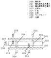
図2は本発明の液晶表示装置で光利用効率が向上することを示す原理図である。図2において、光源207から無偏光で出射した光源光203が、偏光選択反射層A201に入射すると、偏光選択反射層A201を直線偏光のS波205は透過するがP波204は反射する。反射したP波204は偏光選択反射層B202に入射する。このとき、偏光選択反射層B202がP波を透過しS波を反射する構成であれば、偏光選択反射層A201からの反射光は偏光選択反射層B202を透過する。このため原理的に光源光203は偏光選択反射層A201、または偏光選択反射層B202のどちらかを透過することになる。このため、従来の吸収型偏光層を用いる場合に比べ光利用効率が大幅に向上する。なお、偏光の選択性はP波とS波以外にも左円偏光と右円偏光に対して選択性を有しても良い。偏光選択反射層A201と偏光選択反射層B202で偏光選択性が互いに異なれば、同様の効果が得られる。
【0018】
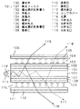
図1は本発明の第1の液晶表示装置の断面図である。光源114を出射した光の一部は、集光フィルム101で法線方向に集光された後、偏光選択反射層A102に入射する。偏光選択反射層A102は、P波を反射しS波を透過する構成を有している。このため、S波は液晶A104を透過し、基板B105から出射する(出射光A115)。一方、P波は偏光選択反射層A102で反射して、偏光選択反射層B108に入射する。偏光選択反射層B108はP波を透過しS波を反射する構成を有している。このため、偏光選択反射層A102からの反射光(P波)は偏光選択反射層B108を透過し、基板D111から出射する(出射光B116)。
【0019】
一方、光源から偏光選択反射層B108に入射した光も同様の原理で、P波は出射光C117と成り、S波は出射光D118と成る。このため光源の光は吸収されること無く基板B105、又は基板D111の一方から出射されることに成り、光利用効率が向上する。
【0020】
P波とS波の偏光選択反射層としては、例えばD−BEF(3M社製)を用いることができる。また、円偏光に対する偏光選択性を利用しても良く、例えばコレステリック液晶ポリマー素子等を用いることができる。
【0021】
また、集光フィルムを用いることで、光源光が法線方向に集光され偏光選択性が向上する。これは、偏光選択反射層の偏光選択性には入射角度依存性があり、法線方向が最も偏光選択性が高いためである。
【0022】
上記は透過型の液晶表示装置の構成であるが、これは画素の一部に開口を有するか、半透過膜を用いた半透過型液晶表示装置の構成でも良い。また、導光体を挟んだ一方が透過型で他方が半透過型でも良い。
【0023】
また、導光体を挟んで配置された液晶パネルの一方が透過型液晶パネルか半透過型パネルで、他方が反射型パネルでも良い。この場合、両面表示は出来ないが、片側から表示面を観察する場合に、必要に応じて反射型表示と透過型(又は半透過型)表示を切り替えることができる。このため反射型で低消費電力、透過型で高品位表示と目的に応じて使い分けが可能である。
【0024】
(実施の形態2)
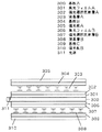
図3は本発明の第2の液晶表示装置の断面図を示す。基板A300の両側に偏光選択反射層と液晶層を形成し、基板A300の端部に光源311が埋め込まれている。基板A300は液晶の保持機能と導光体の機能を兼用している。このとき、実施の形態1に示した導光体が不要となり薄型化が図れる。
【0025】
基板A300の表面には、光源光が基板内を均一に導光するように微小な凹凸構造を設けても良い。凹凸構造としては、溝状、ドット状、または半円柱状等の凹凸構造を、面内輝度が均一となるように大きさと分布密度を適時変えて用いることができる。
【0026】
(実施の形態3)
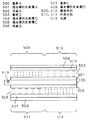
図4は本発明の第3の液晶表示装置の断面図を示す。実施の形態1と同様の構成において、基板C421の外側に偏光選択反射層D422、基板D411の外側に偏光選択反射層C412を形成した。また、偏光選択反射層A402と偏光選択反射層B408は異なる偏光選択反射性を有する。さらに、偏光選択反射層A402と偏光選択反射層D422、及び偏光選択反射層B408と偏光選択反射層C412も異なる偏光選択反射性を有する。具体的には、偏光選択反射層A402と偏光選択反射層C412は、S波を透過してP波を反射する。また、偏光選択反射層D422と偏光選択反射層B408は、P波を透過してS波を反射する。また、液晶A404、液晶B410は黒表示時に液晶層を通過する光に対して位相が変調せず白表示時に位相変調を行う表示モードとする。本構成により、パネルの黒表示部に相当する位置の液晶層に入射した光源光は導光体側に反射され、導光体の反対側に位置する液晶層の白表示部から出射することが可能と成る。このため、光利用効率がさらに向上する。
【0027】
偏光選択反射層A402を透過したS波のうち、黒表示部405に入射した光は、液晶層で位相変調を受けない。このため偏光選択反射層D422にS波のまま入射し、導光体側に反射されて反対側の白表示部413から出射する。また、白表示部406に入射した光は液晶A404で位相変調(S波→P波)を受けるため基板C421側から出射する(出射光B418)。
【0028】
液晶層の表示モードには、ノーマリブラックモードの場合は横電界で駆動するホモジニアス配向や、垂直配向モードを用いることができる。また、捻れネマチック配向の場合は、ノーマリホワイトモードで用いると黒表示時に位相変調が小さく良好な偏光選択性が得られる。
【0029】
(実施の形態4)
図5は本発明の第4の液晶表示装置の断面図である。実施の形態2とほぼ同様の構成で、基板B503の外側に偏光選択反射層B504、基板C507の外側に偏光選択反射層D508を形成した。また、偏光選択反射層A501と偏光選択反射層C505は異なる偏光選択反射性を有する。さらに、偏光選択反射層A501と偏光選択反射層B504、及び偏光選択反射層C505と偏光選択反射層D508も異なる偏光選択反射性を有する。具体的には、偏光選択反射層A501と偏光選択反射層D508は、S波を透過してP波を反射する。また、偏光選択反射層C505と偏光選択反射層B504は、P波を透過してS波を反射する。
【0030】
また、液晶A502、液晶B506は黒表示時に液晶層を通過する光に対して位相が変調せず白表示時に位相変調を行う表示モードとする。本構成により、実施の形態3と同様の原理で光利用効率が向上する。
【0031】
以下の実施の形態5、及び6の液晶表示装置は基板の片側に表示部を有する液晶表示装置である。
【0032】
(実施の形態5)
図6は本発明の第1の立体視表示装置の構成図である。導光体900に液晶パネルA901と液晶パネルB902が積層された実施の形態1記載の液晶表示装置が配置されている。表示面に対面して、光路変更機構として反射板A904、反射板B905、光学素子A906、及び光学素子B907が配置されている。光学素子は、表示面の信号をスクリーン908上に均一に照射する機能を有している。また、液晶表示装置は両面の表示面がそれぞれ右目信号と左目信号を表示する。信号は上記の光路変更機構により、スクリーン908上で合成されることで立体視が可能となる。
【0033】
液晶表示装置は、実施形態1から4記載の液晶表示装置の何れかを用いれば良い。また、光路変更機構は上記以外にもスクリーン上で右目信号と左目信号が合成できるように形成できる。
【0034】
(実施の形態6)
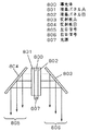
図7は本発明の第2の立体視表示装置の構成図である。導光体800、液晶パネルA801、及び液晶パネルB802等から成る実施の形態1記載の液晶表示装置が配置されている。また、反射板A803、及び反射板B804から成る光路変更機構が形成されている。このとき、液晶表示装置の両側の表示部がそれぞれ右目信号と左目信号を表示し、光路変更機構により、右目信号と左目信号が別個にそれぞれ右目と左目に入射する構成とすることで、立体視を行うことが可能となる。
【0035】
(実施の形態7)
本発明の第3の立体視表示装置は、実施の形態5と同様の構成において、液晶表示装置の両側の表示部が、それぞれ目の焦点深度が異なる状態に対応する表示情報を表示する。目の焦点深度が異なる画像を合成すると立体視を行うことが可能となる。
【0036】
【発明の効果】
以上、本発明によれば、両面表示、又は片面表示の液晶表示装置の光利用効率が向上し高輝度化と低電力化が図れる。また、基板に導光体機能を付与することで、薄型化が図れる。
【図面の簡単な説明】
【図1】実施の形態1の液晶表示装置の断面図
【図2】光利用効率の向上の原理図
【図3】実施の形態2の液晶表示装置の断面図
【図4】実施の形態3の液晶表示装置の断面図
【図5】実施の形態4の液晶表示装置の断面図
【図6】実施の形態5の立体視表示装置の構成図
【図7】実施の形態6の立体視表示装置の構成図
【符号の説明】
100 導光体
101 集光フィルム
102 偏光選択反射層A
103 基板A
104 液晶A
105 基板B
106 偏光板A
107 集光フィルム
108 偏光選択反射層B
109 基板C
110 液晶B
111 基板D
112 偏光板B
113 ランプカバー
114 光源
115 出射光A
116 出射光B
117 出射光C
118 出射光D[0001]
BACKGROUND OF THE INVENTION
The present invention relates to a liquid crystal display device and a stereoscopic display device that can realize high luminance at low cost.
[0002]
[Prior art]
A liquid crystal display device capable of displaying on both sides, such as paper, has been realized by bonding two liquid crystal display devices together.
[0003]
On the other hand, the conventional stereoscopic display device displays two liquid crystal panels arranged in parallel or time-division driving and combining the information of the right eye and the left eye.
[0004]
[Problems to be solved by the invention]
When two liquid crystal display devices are bonded to perform double-sided display, two sets of liquid crystal display devices are required, and cost reduction is difficult. Moreover, there also existed the subject that thickness increased. Further, the liquid crystal display device capable of displaying on both sides uses an absorption type polarizing plate, and it has not been possible to reduce power consumption and brightness.
[0005]
On the other hand, in the conventional stereoscopic display device using a plurality of liquid crystal panels, it is difficult to reduce power consumption because the same number of backlights are required. In addition, a stereoscopic display device that performs stereoscopic viewing by time-division driving has a problem that luminance decreases due to time-division driving.
[0006]
[Means for Solving the Problems]
In order to solve the above problems, the following measures were taken in a double-sided display type liquid crystal display device and a stereoscopic display device using the same.
[0007]
The first liquid crystal display device of the present invention is a liquid crystal display device in which a liquid crystal panel is disposed on both sides of a light guide, wherein a polarization selective reflection layer is disposed between the light guide and the liquid crystal panel, and further on both sides of the light guide. The polarization selective reflection layers have different polarization selectivity. By arranging the liquid crystal display panels on both sides of the light guide, only one light guide is required, and the cost can be reduced. At this time, if one of the liquid crystal panels is a transflective liquid crystal panel and the other is a transmissive liquid crystal panel, a necessary display quality can be realized depending on the situation of viewing the display surface. For example, in a folding mobile phone, if the front surface of the lid is a transflective panel and the back surface is the transmissive panel side, only the transflective panel with excellent power consumption is driven during standby. A transmissive panel on the back side can be used for high quality display .
[0008]
As the polarization selective reflection layer, for example, one that transmits the P wave and reflects the S wave is provided on one side of the light guide, and the other side that transmits the S wave and reflects the P wave is provided. In this case, the reflected light reflected by one polarization selective reflection layer can pass through the other polarization selective reflection layer. Therefore, even if the liquid crystal panels are stacked on both sides of the light guide, the backlight light is efficiently incident on one of the liquid crystal panels without being absorbed. For this reason, low power and high luminance can be achieved. At this time, the same effect can be obtained even if the polarization selective reflection layer has polarization selectivity with respect to circularly polarized light.
[0009]
In the second liquid crystal display device of the present invention, the first liquid crystal layer and the second substrate are formed on one side of the first substrate on which the light source is disposed, and the second liquid crystal layer and the third substrate are formed on the other side of the first substrate. In the liquid crystal display device in which the substrate is formed, a polarization selective reflection layer is laminated between the first substrate and the first liquid crystal layer, and between the first substrate and the second liquid crystal layer, and the polarization selective reflection layer is mutually formed on both sides of the first substrate. It is characterized by having different polarization selectivity. Without using a light guide separately, the substrate holding the liquid crystal layer itself can have a light guide function, and a polarization selective reflection layer can be attached to the substrate to reduce the thickness.
[0010]
In the third liquid crystal display device of the present invention, a first liquid crystal panel is laminated on one side of a light guide provided with a light source, and the first liquid crystal panel includes a first polarization selective reflection layer and a first liquid crystal from the light guide side. And a second polarization selective reflection layer, and a second liquid crystal panel is laminated on the other surface of the light guide, and the second liquid crystal panel has a third polarization selective reflection layer and a second liquid crystal layer from the light guide side. And the fourth polarized light selective reflection layer, the first polarized light selective reflection layer and the third polarized light selective reflection layer have different polarization selectivity, and further the first polarized light selective reflection layer and the second polarized light selective reflection layer. The third polarization selective reflection layer and the fourth polarization selective reflection layer have different polarization selectivity from each other. With this configuration, it becomes possible for light incident on the black display portions of the first liquid crystal panel and the second liquid crystal panel to be incident on the light guide again, thereby further improving light utilization efficiency.
[0011]
The fourth liquid crystal display device of the present invention includes a first polarized light selective reflection layer, a first liquid crystal layer, and a second polarized light selective reflection layer from the first substrate side on one side of the first substrate in which a light source is disposed near the end surface. And the second substrate, and the third polarization selective reflection layer, the second liquid crystal layer, the fourth polarization selective reflection layer, and the third substrate are formed on the other surface side of the first substrate from the first substrate side. In the display device, the first polarization selective reflection layer and the third polarization selective reflection layer have different polarization selectivity, and the first polarization selective reflection layer, the second polarization selective reflection layer, and the third polarization selective reflection layer, The fourth polarization selective reflection layers have different polarization selectivity from each other. This configuration improves the light utilization efficiency for the same reason as in the third liquid crystal display device.
[0012]
The first stereoscopic display device of the present invention is a stereoscopic display device comprising any optical path changing mechanism of
[0013]
Second stereoscopic display device of the present invention, with any one of
[0014]
Stereoscopic vision can be obtained even if the signal is incident on the right eye and the left eye separately.
[0015]
Third stereoscopic display device of the present invention is a stereoscopic display device comprising any optical path changing mechanism of
[0016]
DETAILED DESCRIPTION OF THE INVENTION
The following liquid crystal display devices of
[0017]
(Embodiment 1)
FIG. 2 is a principle view showing that the light use efficiency is improved in the liquid crystal display device of the present invention. In FIG. 2, when the
[0018]
FIG. 1 is a cross-sectional view of a first liquid crystal display device of the present invention. A part of the light emitted from the
[0019]
On the other hand, the light incident on the polarization selective reflection layer B108 from the light source also has the same principle, the P wave becomes the outgoing light C117, and the S wave becomes the outgoing light D118. For this reason, the light of the light source is emitted from one of the substrate B105 and the substrate D111 without being absorbed, and the light use efficiency is improved.
[0020]
For example, D-BEF (manufactured by 3M) can be used as the P wave and S wave polarization selective reflection layer. Moreover, you may utilize the polarization selectivity with respect to circularly polarized light, for example, a cholesteric liquid crystal polymer element etc. can be used.
[0021]
Moreover, by using a condensing film, light source light is condensed in the normal direction and polarization selectivity is improved. This is because the polarization selectivity of the polarization selective reflection layer has an incident angle dependency and the normal direction has the highest polarization selectivity.
[0022]
The above is a configuration of a transmissive liquid crystal display device, but this may be a configuration of a transflective liquid crystal display device having an opening in a part of a pixel or using a transflective film. One of the light guides may be transmissive and the other may be transflective.
[0023]
One of the liquid crystal panels arranged with the light guide interposed therebetween may be a transmissive liquid crystal panel or a transflective panel, and the other may be a reflective panel. In this case, double-sided display is not possible, but when observing the display surface from one side, it is possible to switch between reflective display and transmissive (or transflective) display as necessary. For this reason, the reflective type and the low power consumption, the transmissive type and the high-quality display can be used depending on the purpose.
[0024]
(Embodiment 2)
FIG. 3 is a sectional view of the second liquid crystal display device of the present invention. A polarization selective reflection layer and a liquid crystal layer are formed on both sides of the substrate A300, and a
[0025]
A minute concavo-convex structure may be provided on the surface of the substrate A300 so that the light source light is uniformly guided through the substrate. As the concavo-convex structure, a concavo-convex structure such as a groove shape, a dot shape, or a semi-cylindrical shape can be used by appropriately changing the size and distribution density so that the in-plane luminance is uniform.
[0026]
(Embodiment 3)
FIG. 4 shows a sectional view of a third liquid crystal display device of the present invention. In the same configuration as in the first embodiment, the polarization selective reflection layer D422 is formed outside the substrate C421, and the polarization selective reflection layer C412 is formed outside the substrate D411. Further, the polarization selective reflection layer A402 and the polarization selective reflection layer B408 have different polarization selective reflection properties. Furthermore, the polarization selective reflection layer A402 and the polarization selective reflection layer D422, and the polarization selective reflection layer B408 and the polarization selective reflection layer C412 also have different polarization selective reflection properties. Specifically, the polarization selective reflection layer A402 and the polarization selective reflection layer C412 transmit the S wave and reflect the P wave. Further, the polarization selective reflection layer D422 and the polarization selective reflection layer B408 transmit the P wave and reflect the S wave. Further, the liquid crystal A404 and the liquid crystal B410 are set to a display mode in which the phase is not modulated with respect to the light passing through the liquid crystal layer at the time of black display and the phase is modulated at the time of white display. With this configuration, light source light incident on the liquid crystal layer at a position corresponding to the black display portion of the panel is reflected to the light guide side and can be emitted from the white display portion of the liquid crystal layer located on the opposite side of the light guide body. It becomes. For this reason, the light utilization efficiency is further improved.
[0027]
Of the S waves transmitted through the polarization selective reflection layer A402, the light incident on the
[0028]
As the display mode of the liquid crystal layer, homogeneous alignment driven by a lateral electric field or vertical alignment mode can be used in the normally black mode. In the case of twisted nematic orientation, when used in the normally white mode, phase modulation is small during black display and good polarization selectivity can be obtained.
[0029]
(Embodiment 4)
FIG. 5 is a sectional view of a fourth liquid crystal display device of the present invention. In the same configuration as in the second embodiment, a polarization selective reflection layer B504 is formed outside the substrate B503, and a polarization selective reflection layer D508 is formed outside the substrate C507. The polarization selective reflection layer A501 and the polarization selective reflection layer C505 have different polarization selective reflectivities. Further, the polarization selective reflection layer A501 and the polarization selective reflection layer B504, and the polarization selective reflection layer C505 and the polarization selective reflection layer D508 also have different polarization selective reflection properties. Specifically, the polarization selective reflection layer A501 and the polarization selective reflection layer D508 transmit the S wave and reflect the P wave. Further, the polarization selective reflection layer C505 and the polarization selective reflection layer B504 transmit the P wave and reflect the S wave.
[0030]
Further, the liquid crystal A502 and the liquid crystal B506 are set to a display mode in which the phase is not modulated with respect to light passing through the liquid crystal layer at the time of black display and phase modulation is performed at the time of white display. With this configuration, the light utilization efficiency is improved on the same principle as in the third embodiment.
[0031]
The liquid crystal display devices of the following fifth and sixth embodiments are liquid crystal display devices having a display portion on one side of a substrate.
[0032]
(Embodiment 5)
FIG. 6 is a block diagram of the first stereoscopic display apparatus of the present invention. The liquid crystal display device described in
[0033]
As the liquid crystal display device, any one of the liquid crystal display devices described in
[0034]
(Embodiment 6)
FIG. 7 is a configuration diagram of the second stereoscopic display apparatus of the present invention. The liquid crystal display device according to the first embodiment including the
[0035]
(Embodiment 7)
In the third stereoscopic display device of the present invention, in the same configuration as in the fifth embodiment, the display units on both sides of the liquid crystal display device display the display information corresponding to the different depths of focus of the eyes. Stereoscopy can be performed by synthesizing images with different depths of focus of eyes.
[0036]
【The invention's effect】
As described above, according to the present invention, the light use efficiency of the liquid crystal display device for double-sided display or single-sided display is improved, and high luminance and low power can be achieved. Further, by providing the substrate with a light guide function, the thickness can be reduced.
[Brief description of the drawings]
FIG. 1 is a cross-sectional view of a liquid crystal display device according to a first embodiment. FIG. 2 is a principle diagram for improving light utilization efficiency. FIG. 3 is a cross-sectional view of a liquid crystal display device according to a second embodiment. FIG. 5 is a cross-sectional view of a liquid crystal display device according to a fourth embodiment. FIG. 6 is a configuration diagram of a stereoscopic display device according to a fifth embodiment. FIG. 7 is a stereoscopic display according to the sixth embodiment. System configuration [Explanation of symbols]
100
103 Substrate A
104 Liquid crystal A
105 Substrate B
106 Polarizing plate A
107
109 Substrate C
110 Liquid crystal B
111 Substrate D
112 Polarizing plate B
113
116 Outgoing light B
117 Outgoing light C
118 Outgoing light D
Claims (13)
Priority Applications (1)
| Application Number | Priority Date | Filing Date | Title |
|---|---|---|---|
| JP2000386626A JP4119085B2 (en) | 2000-12-20 | 2000-12-20 | Liquid crystal display device and stereoscopic display device |
Applications Claiming Priority (1)
| Application Number | Priority Date | Filing Date | Title |
|---|---|---|---|
| JP2000386626A JP4119085B2 (en) | 2000-12-20 | 2000-12-20 | Liquid crystal display device and stereoscopic display device |
Publications (2)
| Publication Number | Publication Date |
|---|---|
| JP2002189230A JP2002189230A (en) | 2002-07-05 |
| JP4119085B2 true JP4119085B2 (en) | 2008-07-16 |
Family
ID=18853693
Family Applications (1)
| Application Number | Title | Priority Date | Filing Date |
|---|---|---|---|
| JP2000386626A Expired - Fee Related JP4119085B2 (en) | 2000-12-20 | 2000-12-20 | Liquid crystal display device and stereoscopic display device |
Country Status (1)
| Country | Link |
|---|---|
| JP (1) | JP4119085B2 (en) |
Families Citing this family (31)
| Publication number | Priority date | Publication date | Assignee | Title |
|---|---|---|---|---|
| US6925313B2 (en) | 2001-02-07 | 2005-08-02 | Hyundai Curitel Inc. | Folder-type mobile communication terminal having double-sided LCD |
| US7198028B2 (en) | 2001-07-18 | 2007-04-03 | Walbro Engine Management, L.L.C. | Ignition timing control system for light duty combustion engines |
| WO2003029884A1 (en) * | 2001-09-28 | 2003-04-10 | Citizen Watch Co., Ltd. | Liquid crystal display device |
| KR100432009B1 (en) * | 2001-12-03 | 2004-05-22 | 주식회사 팬택 | Dual way display type liquid crystal display device for a mobile communication apparatus |
| JP3599022B2 (en) | 2002-01-10 | 2004-12-08 | カシオ計算機株式会社 | Liquid crystal display |
| SE524047C2 (en) * | 2002-03-07 | 2004-06-22 | Flir Systems Ab | Method and apparatus for bi-monocular image transfer |
| JP2009175756A (en) * | 2002-04-30 | 2009-08-06 | Casio Comput Co Ltd | Liquid crystal display |
| JP2004021238A (en) | 2002-06-20 | 2004-01-22 | Nec Saitama Ltd | Display device and mobile terminal system |
| KR100828531B1 (en) * | 2002-07-26 | 2008-05-13 | 삼성전자주식회사 | Liquid crystal display |
| TWI232281B (en) | 2002-08-16 | 2005-05-11 | Toppoly Optoelectronics Corp | A backlight device of a LCD display |
| JP2004199027A (en) | 2002-10-24 | 2004-07-15 | Seiko Epson Corp | Display device and electronic equipment |
| JP3719433B2 (en) | 2002-10-30 | 2005-11-24 | セイコーエプソン株式会社 | Display device and electronic device |
| US7102162B2 (en) * | 2002-12-12 | 2006-09-05 | Che-Kuei Mai | Plane light source structure for planar display |
| KR100506088B1 (en) | 2003-01-14 | 2005-08-03 | 삼성전자주식회사 | Liquid crystal displaying apparatus |
| JP3873256B2 (en) | 2003-01-24 | 2007-01-24 | ミネベア株式会社 | Surface lighting device |
| JP4026135B2 (en) * | 2003-02-20 | 2007-12-26 | ミネベア株式会社 | Surface lighting device |
| TWI363573B (en) * | 2003-04-07 | 2012-05-01 | Semiconductor Energy Lab | Electronic apparatus |
| US7015989B2 (en) * | 2003-05-12 | 2006-03-21 | Lg.Philips Lcd Co., Ltd. | Liquid crystal display device using dual light unit |
| JP4776898B2 (en) * | 2003-08-01 | 2011-09-21 | 株式会社半導体エネルギー研究所 | vehicle |
| US7772756B2 (en) | 2003-08-01 | 2010-08-10 | Semiconductor Energy Laboratory Co., Ltd. | Light-emitting device including a dual emission panel |
| JP4055741B2 (en) * | 2004-05-24 | 2008-03-05 | セイコーエプソン株式会社 | Electro-optical device and electronic apparatus |
| KR20060034528A (en) * | 2004-10-19 | 2006-04-24 | 삼성전자주식회사 | Display device that can adjust the height of display panel |
| TWI386744B (en) | 2004-12-14 | 2013-02-21 | 三星顯示器公司 | Thin film transistor panel and liquid crystal display using the same |
| US20060152648A1 (en) * | 2005-01-12 | 2006-07-13 | Samsung Electronics Co., Ltd. | Display device and portable display apparatus including the same |
| JP2006323315A (en) | 2005-05-20 | 2006-11-30 | Citizen Electronics Co Ltd | Combined front-rear backlight |
| KR100796591B1 (en) * | 2005-08-23 | 2008-01-21 | 삼성에스디아이 주식회사 | Double-sided stereoscopic image display device |
| WO2007040028A1 (en) * | 2005-10-04 | 2007-04-12 | Sharp Kabushiki Kaisha | Liquid crystal display unit and portable electronic apparatus provided with it |
| KR101148197B1 (en) * | 2005-12-19 | 2012-05-23 | 삼성전자주식회사 | Dual display apparatus |
| JP4083785B2 (en) * | 2007-02-24 | 2008-04-30 | セイコーインスツル株式会社 | Liquid crystal display |
| KR101942786B1 (en) * | 2011-12-15 | 2019-01-29 | 엘지디스플레이 주식회사 | Bidirectional display device |
| KR102553840B1 (en) * | 2016-08-31 | 2023-07-10 | 삼성전자주식회사 | Glassless three-dimensional display apparatus including single back light unit |
-
2000
- 2000-12-20 JP JP2000386626A patent/JP4119085B2/en not_active Expired - Fee Related
Also Published As
| Publication number | Publication date |
|---|---|
| JP2002189230A (en) | 2002-07-05 |
Similar Documents
| Publication | Publication Date | Title |
|---|---|---|
| JP4119085B2 (en) | Liquid crystal display device and stereoscopic display device | |
| TWI309738B (en) | ||
| JP4042516B2 (en) | Display device | |
| JP4408368B2 (en) | DISPLAY DEVICE, DISPLAY METHOD, AND DEVICE USING THEM | |
| EP1950980B1 (en) | Autostereoscopic 2D/3D switchable display apparatus with high light efficiency, employing a lenticular screen and time-multiplexing of 3D-views | |
| JP3419766B2 (en) | Apparatus that can switch between image display state and mirror state, and equipment equipped with this | |
| CN202995195U (en) | Liquid crystal display device, special glasses and privacy display device | |
| JP4044369B2 (en) | Liquid crystal display | |
| CN102466917B (en) | Liquid crystal indicator | |
| CN101276091A (en) | Liquid crystal display device and terminal device with touch panel | |
| KR20120138236A (en) | Bendable liquid crystal polarization switch for direct view stereoscopic display | |
| TW594194B (en) | Liquid crystal display device and electronic device | |
| JP4742300B2 (en) | Display device | |
| US8456596B2 (en) | Transparent display device and displaying method using the same | |
| JPH1184115A (en) | Reflector, liquid crystal device and electronic equipment | |
| JP2010211084A (en) | Display device | |
| JP2007127724A (en) | Liquid crystal display device | |
| JP2003202565A (en) | Apparatus capable of switching between image display state and mirror state, and equipment provided with this | |
| US8866979B2 (en) | Display device with parallax barrier | |
| US20060055838A1 (en) | Light recycling film and display | |
| TW594263B (en) | Optical device and display | |
| WO2004029704A1 (en) | Reflective/transmissive type liquid crystal display panel, 2d/3d switching liquid crystal display panel, and 2d/3d switching liquid crystal display unit | |
| JP4176816B2 (en) | Liquid crystal display | |
| CN100504535C (en) | Display device and display device mounting device | |
| CN108227319A (en) | A kind of display panel and display device |
Legal Events
| Date | Code | Title | Description |
|---|---|---|---|
| A711 | Notification of change in applicant |
Free format text: JAPANESE INTERMEDIATE CODE: A711 Effective date: 20061109 |
|
| A621 | Written request for application examination |
Free format text: JAPANESE INTERMEDIATE CODE: A621 Effective date: 20070820 |
|
| A131 | Notification of reasons for refusal |
Free format text: JAPANESE INTERMEDIATE CODE: A131 Effective date: 20070904 |
|
| A521 | Written amendment |
Free format text: JAPANESE INTERMEDIATE CODE: A523 Effective date: 20071030 |
|
| A131 | Notification of reasons for refusal |
Free format text: JAPANESE INTERMEDIATE CODE: A131 Effective date: 20080205 |
|
| A521 | Written amendment |
Free format text: JAPANESE INTERMEDIATE CODE: A523 Effective date: 20080327 |
|
| TRDD | Decision of grant or rejection written | ||
| A01 | Written decision to grant a patent or to grant a registration (utility model) |
Free format text: JAPANESE INTERMEDIATE CODE: A01 Effective date: 20080422 |
|
| A61 | First payment of annual fees (during grant procedure) |
Free format text: JAPANESE INTERMEDIATE CODE: A61 Effective date: 20080424 |
|
| R150 | Certificate of patent or registration of utility model |
Free format text: JAPANESE INTERMEDIATE CODE: R150 |
|
| FPAY | Renewal fee payment (event date is renewal date of database) |
Free format text: PAYMENT UNTIL: 20110502 Year of fee payment: 3 |
|
| S533 | Written request for registration of change of name |
Free format text: JAPANESE INTERMEDIATE CODE: R313533 |
|
| FPAY | Renewal fee payment (event date is renewal date of database) |
Free format text: PAYMENT UNTIL: 20110502 Year of fee payment: 3 |
|
| R350 | Written notification of registration of transfer |
Free format text: JAPANESE INTERMEDIATE CODE: R350 |
|
| FPAY | Renewal fee payment (event date is renewal date of database) |
Free format text: PAYMENT UNTIL: 20110502 Year of fee payment: 3 |
|
| FPAY | Renewal fee payment (event date is renewal date of database) |
Free format text: PAYMENT UNTIL: 20120502 Year of fee payment: 4 |
|
| S531 | Written request for registration of change of domicile |
Free format text: JAPANESE INTERMEDIATE CODE: R313531 |
|
| FPAY | Renewal fee payment (event date is renewal date of database) |
Free format text: PAYMENT UNTIL: 20120502 Year of fee payment: 4 |
|
| R350 | Written notification of registration of transfer |
Free format text: JAPANESE INTERMEDIATE CODE: R350 |
|
| FPAY | Renewal fee payment (event date is renewal date of database) |
Free format text: PAYMENT UNTIL: 20120502 Year of fee payment: 4 |
|
| FPAY | Renewal fee payment (event date is renewal date of database) |
Free format text: PAYMENT UNTIL: 20130502 Year of fee payment: 5 |
|
| S533 | Written request for registration of change of name |
Free format text: JAPANESE INTERMEDIATE CODE: R313533 |
|
| FPAY | Renewal fee payment (event date is renewal date of database) |
Free format text: PAYMENT UNTIL: 20130502 Year of fee payment: 5 |
|
| R350 | Written notification of registration of transfer |
Free format text: JAPANESE INTERMEDIATE CODE: R350 |
|
| FPAY | Renewal fee payment (event date is renewal date of database) |
Free format text: PAYMENT UNTIL: 20140502 Year of fee payment: 6 |
|
| R250 | Receipt of annual fees |
Free format text: JAPANESE INTERMEDIATE CODE: R250 |
|
| R250 | Receipt of annual fees |
Free format text: JAPANESE INTERMEDIATE CODE: R250 |
|
| R250 | Receipt of annual fees |
Free format text: JAPANESE INTERMEDIATE CODE: R250 |
|
| LAPS | Cancellation because of no payment of annual fees |