JP4112248B2 - Light emitting device, electronic equipment - Google Patents
Light emitting device, electronic equipment Download PDFInfo
- Publication number
- JP4112248B2 JP4112248B2 JP2002064532A JP2002064532A JP4112248B2 JP 4112248 B2 JP4112248 B2 JP 4112248B2 JP 2002064532 A JP2002064532 A JP 2002064532A JP 2002064532 A JP2002064532 A JP 2002064532A JP 4112248 B2 JP4112248 B2 JP 4112248B2
- Authority
- JP
- Japan
- Prior art keywords
- switch
- transistors
- light
- pixel
- self
- Prior art date
- Legal status (The legal status is an assumption and is not a legal conclusion. Google has not performed a legal analysis and makes no representation as to the accuracy of the status listed.)
- Expired - Fee Related
Links
- 239000003990 capacitor Substances 0.000 claims description 20
- 239000000758 substrate Substances 0.000 claims description 13
- 238000006243 chemical reaction Methods 0.000 claims description 4
- 238000000034 method Methods 0.000 description 34
- 230000003071 parasitic effect Effects 0.000 description 11
- 238000010586 diagram Methods 0.000 description 10
- 239000010408 film Substances 0.000 description 7
- 230000000694 effects Effects 0.000 description 6
- 239000000463 material Substances 0.000 description 6
- 239000004065 semiconductor Substances 0.000 description 6
- 239000010409 thin film Substances 0.000 description 6
- 229910021420 polycrystalline silicon Inorganic materials 0.000 description 5
- 229920005591 polysilicon Polymers 0.000 description 5
- 239000004020 conductor Substances 0.000 description 4
- 239000004973 liquid crystal related substance Substances 0.000 description 4
- 239000011159 matrix material Substances 0.000 description 4
- 238000012360 testing method Methods 0.000 description 4
- 230000007547 defect Effects 0.000 description 3
- 230000005669 field effect Effects 0.000 description 3
- 238000004519 manufacturing process Methods 0.000 description 3
- 150000002894 organic compounds Chemical class 0.000 description 3
- 150000001875 compounds Chemical class 0.000 description 2
- 229910010272 inorganic material Inorganic materials 0.000 description 2
- 239000011147 inorganic material Substances 0.000 description 2
- 238000005259 measurement Methods 0.000 description 2
- 239000007787 solid Substances 0.000 description 2
- 230000015556 catabolic process Effects 0.000 description 1
- 230000001413 cellular effect Effects 0.000 description 1
- 238000004040 coloring Methods 0.000 description 1
- 229920001940 conductive polymer Polymers 0.000 description 1
- 239000013078 crystal Substances 0.000 description 1
- 238000006731 degradation reaction Methods 0.000 description 1
- 230000006866 deterioration Effects 0.000 description 1
- 238000011161 development Methods 0.000 description 1
- 239000006185 dispersion Substances 0.000 description 1
- 239000012535 impurity Substances 0.000 description 1
- 239000002184 metal Substances 0.000 description 1
- 230000003287 optical effect Effects 0.000 description 1
- 239000011368 organic material Substances 0.000 description 1
- 229920000642 polymer Polymers 0.000 description 1
- 238000012545 processing Methods 0.000 description 1
- 238000005070 sampling Methods 0.000 description 1
Images


Description
【0001】
【発明の属する技術分野】
本発明は、発光装置及び表示装置の技術に関する。さらには、前記発光装置又は前記表示装置を搭載した電子機器に関する。本明細書における発光装置とは、自発光素子から放出される光を利用した装置を指す。自発光素子としては、有機発光ダイオード(OLED)素子、無機材料系の発光ダイオード素子、電界放出発光素子(FED素子)などを示す。また本明細書における表示装置とは、複数の画素をマトリクス状に配置し画像情報を視覚的に伝達する装置、いわゆるディスプレイを示す。
【0002】
【従来の技術】
近年、画像の表示を行う表示装置の重要性が増している。表示装置としては、液晶素子を用いて画像の表示を行う液晶表示装置が、高画質、薄型、軽量などの利点を活かして、携帯電話やパソコンをはじめとする種々の用途の表示装置として幅広く用いられている。
【0003】
他方で、自発光素子を用いた表示装置、発光装置の開発も進められている。この自発光素子には、有機材料、無機材料、薄膜材料、バルク材料、又は分散材料など広汎に渡って様々な種類の素子が存在する。
【0004】
上記自発光素子のうち、有機発光ダイオード(OLED)素子は、表示装置向けに将来有望視されている。OLED素子を自発光素子として用いたOLED表示装置は、既存の液晶表示装置以上に薄型、軽量である特長に加え、動画表示に適した高応答速度、高視野角、低電圧駆動などの特長を有しているため、携帯電話や携帯情報端末(PDA)をはじめテレビ、モニターなど、幅広い用途が見込まれている。その結果、OLED表示装置は、次世代ディスプレイとして注目されている。
【0005】
特にアクティブマトリクス(以下、AMと表記)型のOLED表示装置は、パッシブマトリクス(以下、PMと表記)型では困難である、高精細で且つ大画面での表示も可能であるうえ、PM型を上回る低消費電力で高信頼性を有しているため、実用化への期待は大変強い。
【0006】
OLED素子は、陽極と、陰極と、該陽極と該陰極との間に挟まれた有機化合物層とを有する構造をしている。そして、OLED素子に流れる電流量と、OLED素子の発光輝度は概ね比例する関係にある。AM型OLED表示装置が有する画素では、該画素のOLED素子の発光輝度を制御する駆動用トランジスタを該OLED素子に直列に接続している場合が多い。
【0007】
ところで、AM型OLED表示装置において画像を表示する駆動方式には、大別して電圧入力方式と電流入力方式がある。前者の電圧入力方式は、画素に入力するビデオ信号として、電圧値形式データのビデオ信号を入力する。また後者の電流入力方式は、画素に入力するビデオ信号として、電流値形式データのビデオ信号を入力する。
【0008】
電圧入力方式では、通常画素の駆動用トランジスタのゲート電極にビデオ信号の電圧が直接印加される。従って、OLED素子を定電流発光させる場合、駆動用トランジスタの電気的特性が各々の画素間で均一でなくバラつきを有していると、各画素のOLED素子駆動電流にバラつきが生じる。OLED素子駆動電流のバラつきは、OLED素子の発光輝度のバラつきとなる。つまり、OLED素子の発光輝度のバラつきは、画面全体でみると砂嵐状あるいは絨毯模様のムラとして、表示画像の品位を低下させる。
【0009】
そこで、電圧入力方式におけるOLED素子駆動電流のバラつきを抑制するための有効な手段の一つとして電流入力方式がある。電流入力方式では、通常ビデオ信号のデータ電流値を記憶し、前記記憶した電流値と同一、又は数倍(1未満を含む正の実数倍)の電流をOLED素子駆動電流として供給する。
【0010】
電流入力方式のAM型OLED表示装置の画素回路の代表的な例を図10(A)に示す(A. Yumoto et al., Proc. Asia Display / IDW '01 p.p.1395-1398 (2001) 等を参照)。図10(A)において、516がOLED素子である。また図10(A)に示す画素回路は、カレントミラー回路を有する。そこで、カレントミラー回路を構成する2つのトランジスタが同一の電気的特性さえ備えていれば、ビデオ信号のデータ電流値を正確に記憶することができる。仮に相異なる画素の駆動用トランジスタの電気的特性にバラつきが生じていても、同一画素内の前記2つのトランジスタが、各々同一の電気的特性を備えていれば、OLED素子の発光輝度のバラつきが抑制されることになる。
【0011】
次いで、図10(A)とは異なる電流入力方式のAM型OLED表示装置の画素回路の例を図10(B)に示す(I. M. Hunter et al., Proc. AM-LCD 2000 p.p.249-252 (2000) 等を参照)。図10(B)において、611がOLED素子である。また図10(B)に示す画素回路は、駆動用トランジスタのゲート電極にビデオ信号に対応する電圧を書込むときに、駆動用トランジスタのドレイン電極とゲート電極とが短絡する。その状態でビデオ信号のデータ電流を流して、その後ゲート電極を電気的に絶縁させる。このとき、OLED素子を発光させるときに、駆動用トランジスタを飽和領域にて動作させるようにすれば、駆動用トランジスタは、書込み時のデータ電流と同一の値の電流をOLED素子に供給する。従って、各画素の駆動用トランジスタに電気的特性のバラつきが存在しても、OLED素子の発光輝度のバラつきは抑制されることになる。
【0012】
【発明が解決しようとする課題】
図10(A)(B)に示す画素は、上述したように正確にデータ電流値を記憶できるはずであるが、以下のような深刻な問題がある。
【0013】
まず、図10(A)の画素回路における問題点は、カレントミラーを構成する二つのトランジスタが同一の電気的特性もつことが、前提条件とされていることである。画素回路の設計時に工夫すれば、両トランジスタを基板上に隣り合わせに作製することも可能であるため、ある程度はバラつきを減少させることが出来る。しかしながら、ポリシリコンで作成されたトランジスタは、結晶粒界における欠陥等に起因して、TFTのしきい値電圧や電界効果移動度等の電気的特性に、なお許容限度を超えるバラつきが残存してしまう。
【0014】
ここで、より具体的に64階調の画像を表示する場合を例に挙げて説明する。64階調の画像を表示する場合には、自発光素子の輝度のバラつきは1%以内程度に抑える必要が生じる。しかし図10(A)の画素回路では、データ電流値を1%の精度で記憶することは、現在普通に使用されるポリシリコンでは困難である。すなわち、図10(A)の画素回路を使うのみでは、画面全体でムラがなく、十分に均一な高品位の表示画像を得ることはできない。
【0015】
次いで、図10(B)の画素回路における問題点は、画素に書込むビデオ信号データ電流と、OLED素子を発光させるときのOLED素子駆動電流とが、同一の値になってしまう点である。AM型OLED表示装置を作製する場合、両電流を同一の値としなくてはならないという点は、事実上はかなり厳しい制約となる。
【0016】
これは、AM型OLED表示装置において、信号線等に多量の寄生容量、寄生抵抗がついてしまうことによるものである。多量の寄生容量、寄生抵抗がついてしまうと、ビデオ信号データ電流はOLED素子駆動電流よりも大きくする措置をとることが必要な場合が少なからず生じる。特に、ビデオ信号データ電流をアナログ値にして階調表現する場合には、暗部のビデオ信号データ電流の書込みが非常に困難となる。
【0017】
本発明は上記問題点の存在に鑑みてなされたものである。まず本発明は、図10(B)の画素回路とは異なり、画素に書込むビデオ信号データ電流と、OLED素子を発光させるときのOLED素子駆動電流との比が「1」に固定されないAM型OLED表示装置を提供することを課題とする。次に本発明は、図10(A)の画素回路とは異なり、同一画素内の隣接設置されたトランジスタ間においても、なお電気的特性のバラつきがある程度残存することを前提とする。その上で本発明は、図10(A)のようなカレントミラーを用いた画素回路の場合と比較して、OLED素子駆動電流のバラつきが十分に抑制されたAM型OLED表示装置を提供することを課題とする。
【0018】
また、自発光素子は有機化合物層の劣化によって生じる信頼性等の低さが問題となっている。そこで本発明は、自発光素子の信頼性の問題を改善した表示装置、発光装置を提供することを課題とする。
【0019】
【課題を解決するための手段】
上記課題を解決するために、本発明はAM型表示装置または発光装置において、各画素に設置される駆動用素子を複数のトランジスタにより構成し、画素にデータ電流を読込むときには該複数のトランジスタを並列接続状態にし、自発光素子を発光させるときには該複数のトランジスタを直列接続状態にすることを特徴としている。
【0020】
なおOLED素子以外の素子を用いた表示装置、発光装置であっても、電流駆動型の素子を用いる場合には、本発明の構成が利用できる。
【0021】
また本発明は、上記課題を解決するために、一定の期間ごとに発光時とは逆の極性の駆動電圧(逆方向バイアス電圧)を発光素子に印加することを特徴としている。これは、逆の極性の駆動電圧を発光素子に印加すると、発光素子の電流−電圧特性のバラつきが改善されることを利用したものである。
【0022】
本発明は、第1及び第2の電極を有する自発光素子と、
各ゲート電極が共通に接続されたn個(nは2以上の自然数)のトランジスタとを有する駆動手段とが備えられた画素が設けられた発光装置であって、
前記画素に入力されるビデオ信号の同期タイミングに対応して前記n個のトランジスタの各ソース・ドレイン間を直列に接続して電流IWを流し、前記ビデオ信号に応じて、前記n個のトランジスタの各ソース・ドレイン間を並列に接続して前記自発光素子に電流IEを流す設定手段と、
前記ビデオ信号の同期タイミングに対応する単位フレーム期間の所定の期間に対し、前記第1又は前記第2の電極の電位を変化させて、前記自発光素子に逆方向バイアスの電圧を供給する供給手段とを有することを特徴とする。
【0023】
本発明は、第1及び第2の電極を有する自発光素子と、
各ゲート電極が共通に接続されたn個(nは2以上の自然数)のトランジスタとを有する駆動手段とが備えられた画素が設けられた発光装置であって、
前記画素に入力されるビデオ信号の同期タイミングに対応して、前記n個のトランジスタの各ソース・ドレイン間を直列に接続して電流IWを流し、前記ビデオ信号に応じて、前記n個のトランジスタの各ソース・ドレイン間を並列に接続して前記自発光素子に電流IEを流す設定手段と、
前記ビデオ信号の同期タイミングに対応する単位フレーム期間の所定の期間に対し、前記自発光素子の各々の発光期間が所定の発光期間に達したときに前記自発光素子の各々の発光を停止せしめる消去手段と、
前記フレーム期間の所定の期間に対し、前記第1又は前記第2の電極の電位を変化させて、前記自発光素子に逆方向バイアスの電圧を供給する供給手段とを有することを特徴とする。
【0024】
なお前記設定手段とは、画素へのビデオ信号の入力を制御するトランジスタに相当し、より具体的には図1における第1スイッチ12と、第2スイッチ13に相当する。また前記設定手段とは、前記画素を駆動する信号線駆動回路、走査線駆動回路又はコントロール回路に相当する。
さらに、前記駆動手段とは、画素における駆動用トランジスタに相当する。前記駆動用トランジスタは、前記自発光素子を駆動する役目を担っており、多くの場合において、自発光素子に直接接続されているトランジスタを指す。
最後に前記消去手段とは、自発光素子の発光を停止せしめる機能を有し、具体的には図1における第4スイッチ18に相当する。
【0025】
ここで、本発明の表示装置または発光装置の画素構成の概略について、図1(A)(B)を用いて説明する。図1(A)には、複数の画素を有する画素部において、j行i列目に配置された画素11を示す。画素11は、信号線(Si)、電源線(Vi)、第1走査線(Gaj)、スイッチング機能を有する第1スイッチ12〜第3スイッチ14、駆動用素子15、容量素子16、自発光素子17を有する。なお、図1(A)(B)で容量素子16が設置されているノードの寄生容量が大きい場合などには、容量素子16は必ずしも設けなくてよい。
【0026】
また、自発光素子17の第1又は第2の電極は、共通の電源である対向電源19aに接続されている。そして、本発明は、対向電源19aの電位を変化させることで、自発光素子17に逆方向バイアス電圧を印加する。
【0027】
自発光素子としては、典型的にはOLED素子が該当するため、本明細書では、自発光素子を表す記号としてダイオードの記号を用いる。しかし自発光素子にダイオード特性は必須ではなく、本発明はダイオード特性をもつ自発光素子の場合に限定されない。さらに本明細書における自発光素子は、電流駆動型の表示用素子であればよく、自発光により表示機能を担う必要もない。例えば、液晶のような光シャッターの役目を担っている素子であり、且つ電圧値でなく電流値により制御される素子も、本明細書における自発光素子に含まれる。
【0028】
第1スイッチ12〜第3スイッチ14には、トランジスタなどのスイッチング機能を有する半導体素子を1個又は複数個用いることができる。同様に駆動用素子15にも、トランジスタなどの半導体素子を複数個用いることができる。第1スイッチ12及び第2スイッチ13は、第1走査線(Gaj)から与えられる信号により、オン又はオフが決定される。第1スイッチ12及び第2スイッチ13はスイッチとして機能すればよいので、用いられる半導体素子の導電型に特に限定はない。
【0029】
なお第1スイッチ12は、信号線(Si)と駆動用素子15の間に設置されており、画素11に対する信号の書込みを制御する役割を果たす。また第2スイッチ13は、電源線(Vi)と駆動用素子15の間に設置されており、電源線から画素11への電流の供給を制御する。
【0030】
図1(B)には、図1(A)に示した画素11に、第4スイッチ18と第2走査線(Gbj)を追加して配置した場合を示す。第4スイッチ18には、トランジスタなどのスイッチング機能を有する半導体素子を1個又は複数個用いることができる。第4スイッチ18は、第2走査線(Gbj)から与えられる信号により、オン又はオフが決定される。第1スイッチ12及び第2スイッチ13はスイッチとして機能すればよいので、用いられる半導体素子の導電型に特に限定はない。
【0031】
第4スイッチ18は画素11の初期化用素子としての役割を担う。そして、第4スイッチ18がオンになると、容量素子16に保持されている電荷が放出されて、駆動用素子15はオフになり、さらに自発光素子17の発光は終了する。
【0032】
本発明では、駆動用素子15を複数のトランジスタで構成し、画素11にビデオ信号のデータ電流を書込む場合と、自発光素子17に電流を流して発光させる場合とにおいて、該複数のトランジスタの接続を並列と直列とに切替えて用いる点に特徴がある。図1(A)(B)では、第1スイッチ12及び第2スイッチ13を、第1走査線(Gaj)からの信号によりオン・オフの制御を行っていることが、駆動用素子15の複数のトランジスタを、並列接続状態と直列接続状態とを切替える手段となっている。
【0033】
一例として駆動用素子15が4つのトランジスタ20a〜20dで構成された場合の画素11を図1(C)(D)に示し、画素11における動作について以下に説明する。
【0034】
図1(C)は画素11にデータ電流を書込む場合を示し、図1(D)は自発光素子を発光させる場合を示している。なお図1(C)(D)において、第1スイッチ12、第2スイッチ13、駆動用素子15、自発光素子17、信号線(Si)及び電源線(Vi)以外の素子、配線は図示を省略する。
【0035】
最初に、画素11にデータ電流を書込む場合について説明する。図1(C)において、第1スイッチ12及び第2スイッチ13は、第1走査線(Gaj)から与えられる信号によりオンになる。すると駆動用素子15は、各トランジスタがダイオード接続状態となり、かつ相互に並列接続状態になる。電流経路は、電源線(Vi)から第2スイッチ13、駆動用素子15、第1スイッチ12を通って、信号線(Si)に達する経路である。このときの電流値IWは、ビデオ信号のデータ電流値であり、信号線駆動回路(図示せず)が信号線(Si)に出力する所定の電流値である。
【0036】
次いで、自発光素子17を発光させる場合について説明する。図1(D)において、第1スイッチ12及び第2スイッチ13は、第1走査線(Gaj)から与えられる信号によりオフになる。すると駆動用素子15は、各トランジスタが相互に直列接続状態になる。電流経路は、電源線(Vi)からトランジスタ20a、20b、20c、20dを通って自発光素子17に達する経路である。このときの電流値IEにより、自発光素子17の発光輝度が決まる。
【0037】
最後に、自発光素子17に逆方向バイアスを印加する場合について説明する。
【0038】
図1(E)において、対向電源(陰極)19aの電位を陽極の電位よりも高くすることで、自発光素子17に逆方向バイアスを印加することが出来る。なお図1(E)は、対向電源19aからスイッチ14の方向に矢印が図示してある。実際には自発光素子17に逆方向バイアスを印加すると電流は流れないが、図1(E)では説明を分かりやすくするために図示している。
【0039】
上述したように、本発明は、画素にデータ電流を書込むときには、駆動用素子15を構成するトランジスタ20a〜20dを並列に使用する(図1(C))。他方、画素11が有する自発光素子17に電流を流すとき、すなわち自発光素子を駆動しているときには、駆動用素子15を構成するトランジスタ20a〜20dを直列に使用する(図1(D))。従って、トランジスタ20a〜20dの電気的特性が同一であると仮定すれば、書込み時の電流値IWは、自発光素子駆動時の電流値IEの16倍(=42倍)となる。より一般的には、駆動用素子15を構成するトランジスタの数がn個の場合を考えると、該トランジスタの全てが同一の電気的特性をもつの条件の下では、ビデオ信号書込み時の電流値IWと自発光素子駆動時の電流値IEとの間に次式(1)の関係が成立する。
【0040】
【数1】
IW=n2×IE・・・(1)
【0041】
なお式(1)が厳密に成立するためには、駆動用素子15を構成するトランジスタの全てが同一の電気的特性をもつことが条件となる。しかし該トランジスタの電気的特性が、相互に若干のバラつきを伴っている場合であっても、近似的に式(1)が成立するとして扱うことが現実的には可能である。
【0042】
従って本発明では、駆動用素子15を複数のトランジスタで構成し、画素11にビデオ信号電流を書込む場合と、自発光素子を発光させる場合とにおいて、該複数のトランジスタの接続を並列と直列とに切替えて用いることで、書込み時の電流値IWと自発光素子駆動時の電流値IEとを任意に設定することができる特長を有する。
【0043】
また本発明の別の特長として、駆動用素子15を構成する各トランジスタの電気的特性が、相互に若干のバラつきを伴っていたとしても、その影響が自発光素子駆動電流IEに反映されてしまうのを大きく軽減できる点がある。これに関しては、具体的な例を挙げて、実施の形態5において説明する。
【0044】
さらに、図10(A)のようなカレントミラーを用いる画素回路においては、画素内の2つのトランジスタに関する限り、同一の電気的特性もつことが要求されてしまう問題があった。しかしながら本発明では、同一の画素内におけるトランジスタでさえも、相互に電気的特性が若干異なることを既に前提としている。すなわち本発明は、トランジスタの特性バラつきに対する耐性の点において、電流入力方式のカレントミラーを用いる画素回路と比較して優れている。その結果、本発明は、結晶粒界における欠陥等に起因するポリシリコンTFTの電気的特性バラつきが存在しても、自発光素子駆動電流IEを実用レベルにまで均一化することが可能となる。
【0045】
【発明の実施の形態】
(実施の形態1)
以上、本発明の表示装置、発光装置の画素の概略を図1を用いて述べた。実施の形態1では、本発明の表示装置、発光装置の画素の具体的例について、図2〜4を用いて説明する。簡単にするため、駆動用素子15を構成するトランジスタ数nが、2〜4の場合の例を挙げる。
【0046】
最初の例を、図2(A)を用いて説明する。
【0047】
図2(A)には、j行i列目に配置された画素11を示す。そして画素11は、信号線(Si)、電源線(Vi)、走査線(Gaj)、トランジスタ21〜26、容量素子27、自発光素子28を有する。図2(A)に示す画素11は、図1(A)に示す画素11を具体的にトランジスタで図示したものであり、pチャネル型のトランジスタ21、22は第1スイッチ12に相当する。pチャネル型のトランジスタ23は第2スイッチ13に相当し、nチャネル型のトランジスタ24は第3スイッチ14に相当する。pチャネル型のトランジスタ25、26は駆動用素子15に相当する。
【0048】
トランジスタ21〜24の各ゲート電極は、走査線(Gaj)に接続されている。容量素子27は、トランジスタ25のゲート・ソース間電圧を保持する役割を担う。なお、トランジスタ25、26のゲート容量が大きい場合や、該ノードの寄生容量が大きい場合などでは、容量素子27は必ずしも設けなくてもよい。
【0049】
図2(A)に示す画素11に、ビデオ信号データ電流を書込むときには、走査線(Gaj)に低電位信号を送り、トランジスタ21〜23をオン、トランジスタ24をオフにする。このとき、トランジスタ25、26は電流経路上、互いに並列接続の関係になる。一方、自発光素子28に電流を流すときには、走査線(Gaj)に高電位信号を送り、トランジスタ21〜23をオフ、トランジスタ24をオンにする。このとき、トランジスタ25、26は電流経路上、互いに直列接続の関係になる。
【0050】
図2(A)の例では、駆動用素子15のトランジスタ25、26の接続関係の切替えを、第1走査線(Gaj)のみで制御する。また、第1スイッチを2個、第2スイッチを1個のトランジスタのみという、最少個数のトランジスタで構成する。このように図2(A)の例は、走査線数及びトランジスタ数を少なく抑えているため、開口率の確保や歩留まりの向上を重視する場合には好ましい構成である。
【0051】
次いで図2(A)とは別の例を、図2(B)を用いて説明する。
【0052】
図2(B)には、j行i列目に配置された画素11を示す。そして画素11は、信号線(Si)、電源線(Vi)、第1走査線(Gaj)、第2走査線(Gbj)、トランジスタ31〜39、42、容量素子40、自発光素子41を有する。図2(B)に示す画素11は、図1(B)に示す画素11を具体的にトランジスタで図示したものであり、pチャネル型のトランジスタ31〜34は第1スイッチ12に相当する。pチャネル型のトランジスタ35、36は第2スイッチ13に相当し、nチャネル型のトランジスタ37は第3スイッチ14に相当する。pチャネル型のトランジスタ38、39は駆動用素子15に相当する。nチャネル型のトランジスタ42は第4スイッチ18に相当する。
【0053】
トランジスタ31〜34の各ゲート電極は、第1走査線(Gaj)に接続されている。トランジスタ35〜37、42の各ゲート電極は、第2走査線(Gbj)に接続されている。容量素子40は、トランジスタ38のゲート・ソース間電圧を保持する役割を担う。なお、トランジスタ38、39のゲート容量が大きい場合や、該ノードの寄生容量が大きい場合などでは、容量素子40は必ずしも設けなくてもよい。
【0054】
図2(B)に示す画素11に、ビデオ信号データ電流を書込むときには、第1走査線(Gaj)及び第2走査線(Gbj)に低電位信号を送り、トランジスタ31〜36をオン、トランジスタ37、42をオフにする。このとき、トランジスタ38、39は電流経路上、互いに並列接続の関係になる。一方、自発光素子41に電流を流すときには、走査線(Gaj)に高電位信号を送り、トランジスタ31〜36をオフ、トランジスタ37、42をオンにする。このとき、トランジスタ38、39は電流経路上、互いに直列接続の関係になる。
【0055】
図2(B)の例では、駆動用素子15のトランジスタ38、39の接続関係の切替えを、第1走査線(Gaj)及び第2走査線(Gbj)を用いて制御する。しかし第2走査線(Gbj)により制御されるトランジスタは、いずれも信号線(Si)とは接続していない。また自発光素子41に電流を流し発光させるか否かは、第1走査線(Gaj)の電位に関わりなく、第2走査線(Gbj)の電位のみにより制御できる特徴がある。従って、データ電流を書込むとき以外で、第2走査線(Gbj)に第1走査線(Gaj)とは独立の信号を送ることで、自発光素子41の発光時間を任意に制御できる。
【0056】
これは、中間階調表現を時間階調方式により表現する場合に、非常に重要な特長である。ポリシリコンTFTにより形成された駆動回路を有するAM型OLED表示装置に、時間階調方式を適用する場合には、列走査期間中に自発光素子の発光を停止させる手段なしには、十分な多階調表示が困難なためである。また、中間階調表現をアナログ的なビデオ信号データ電流を用いることで表現する場合であっても、ホールド型ディスプレイ特有の動画ボケを防止するために、インパルス型の発光を行う等の用途に有用である(ホールド型ディスプレイ特有の動画ボケについては、例えばT. Kurita, Proc. AM-LCD 2000 p.p.1-4 (2000) 等を参照)。
【0057】
また図2(B)の例の別の特長としては、ビデオ信号データ電流の記憶がより正確に行える点がある。図2(A)の例では、データ電流の書込み時に、トランジスタ25は電源線(Vi)に直接接続するのに対し、トランジスタ26はトランジスタ23を介して接続する。よって、トランジスタ23による電圧降下分だけ、データ電流の書込み時が不正確となる。しかしながら、図2(B)の例では、トランジスタ38はトランジスタ35を介して、トランジスタ39はトランジスタ36を介して、電源線(Vi)に接続する。トランジスタ35とトランジスタ36による電圧降下を、同程度となるようにすれは、ビデオ信号データ電流の記憶をより正確に行うことができる。
【0058】
続いて3つ目の例を、図3(A)を用いて説明する。
【0059】
図3(A)には、j行i列目に配置された画素11を示す。そして画素11は、信号線(Si)、電源線(Vi)、第1走査線(Gaj)、第2走査線(Gbj)、トランジスタ51〜57、60、容量素子58、自発光素子59を有する。図3(A)に示す画素11は、図1(B)に示す画素11を具体的にトランジスタで図示したものであり、nチャネル型のトランジスタ51〜53は第1スイッチ12に相当する。nチャネル型のトランジスタ54は第2スイッチ13に相当し、pチャネル型のトランジスタ55は第3スイッチ14に相当する。pチャネル型のトランジスタ56、57は駆動用素子15に相当する。nチャネル型のトランジスタ60は第4スイッチ18に相当する。
【0060】
トランジスタ51〜55の各ゲート電極は、第1走査線(Gaj)に接続されている。トランジスタ60のゲート電極は、第2走査線(Gbj)に接続されている。容量素子58は、トランジスタ56のゲート・ソース間電圧を保持する役割を担う。なお、トランジスタ56、57のゲート容量が大きい場合や、該ノードの寄生容量が大きい場合などでは、容量素子58は必ずしも設けなくてもよい。
【0061】
図3(A)に示す画素11に、ビデオ信号データ電流を書込むときには、第1走査線(Gaj)に高電位信号を送り、トランジスタ51〜54をオン、トランジスタ55をオフにする。このとき、トランジスタ56、57は電流経路上、互いに並列接続の関係になる。一方、自発光素子59に電流を流すときには、走査線(Gaj)に低電位信号を送り、トランジスタ51〜54をオフ、トランジスタ55をオンにする。このとき、トランジスタ56、57は電流経路上、互いに直列接続の関係になる。
【0062】
なお上記の間、第2走査線(Gbj)には低電位信号を送り、トランジスタ60をオフしておく。
【0063】
図3(A)に示す画素11においても、図2(B)の例の場合と同様に、第2走査線(Gbj)に送る信号により、自発光素子59の発光時間を任意に制御できる。すなわち自発光素子59が発光している間、第2走査線(Gbj)に高電位信号をおくり、トランジスタ60をオンにすると、トランジスタ56がオフとなって、自発光素子59は消光する。但し、自発光素子59を一度消光させると、再度ビデオ信号データ電流を書込まなくては、自発光素子59を発光させられない。この点は、図2(B)の例と異なる。
【0064】
図3(A)に示す画素11において、自発光素子59の発光時間を任意に制御できることの特長は、図2(B)の例の場合と同様である。すなわち、まず中間階調表現を時間階調方式により表現することが可能となる。また中間階調表現をアナログ的なビデオ信号データ電流を用いることで表現する場合であっても、ホールド型ディスプレイ特有の動画ボケを防止するために、インパルス型の発光を行う等の用途に有用である。
【0065】
図3(A)に示す画素11においては、第1スイッチ12又は第2スイッチ13のトランジスタ51〜54、第4スイッチ18のトランジスタ60はnチャネル型であり、第3スイッチ14のトランジスタ55はpチャネル型である。これは、図2(A)(B)の例の場合と異なっている。しかしこれは、スイッチのトランジスタのチャネル型に関して、特に制限がないことを例示したものにすぎない。
【0066】
続いて4つ目の例を、図3(B)を用いて説明する。
【0067】
図3(B)には、j行i列目に配置された画素11を示す。そして画素11は、信号線(Si)、電源線(Vi)、第1走査線(Gaj)、第2走査線(Gbj)、トランジスタ71〜82、85、容量素子83、自発光素子84を有する。図3(B)に示す画素11は、図1(B)に示す画素11を具体的にトランジスタで図示したものであり、pチャネル型のトランジスタ71〜75は第1スイッチ12に相当する。pチャネル型のトランジスタ76〜78は第2スイッチ13に相当し、nチャネル型のトランジスタ79は第3スイッチ14に相当する。pチャネル型のトランジスタ80〜82は駆動用素子15に相当する。nチャネル型のトランジスタ85は第4スイッチ18に相当する。
【0068】
トランジスタ71〜75、85の各ゲート電極は、第1走査線(Gaj)に接続されている。トランジスタ76〜79のゲート電極は、第2走査線(Gbj)に接続されている。容量素子83は、トランジスタ80のゲート・ソース間電圧を保持する役割を担う。なお、トランジスタ80〜82のゲート容量が大きい場合や、該ノードの寄生容量が大きい場合などでは、容量素子83は必ずしも設けなくてもよい。
【0069】
図3(B)に示す画素11に、ビデオ信号データ電流を書込むときには、第1走査線(Gaj)及び第2走査線(Gbj)に低電位信号を送り、トランジスタ71〜78をオン、トランジスタ79、85をオフにする。このとき、トランジスタ80〜82は電流経路上、互いに並列接続の関係になる。一方、自発光素子84に電流を流すときには、走査線(Gaj)に高電位信号を送り、トランジスタ71〜78をオフ、トランジスタ79、85をオンにする。このとき、トランジスタ80〜82は電流経路上、互いに直列接続の関係になる。
【0070】
図3(B)の例では、駆動用素子15のトランジスタ80〜82の接続関係の切替えを第1走査線(Gaj)及び第2走査線(Gbj)を用いて制御する。しかし第2走査線(Gbj)により制御されるトランジスタは、いずれも信号線(Si)とは接続していない。また自発光素子84に電流を流し発光させるか否かは、第1走査線(Gaj)の電位に関わりなく、第2走査線(Gbj)の電位のみにより制御できる特徴がある。従って、データ電流を書込むとき以外で、第2走査線(Gbj)に第1走査線(Gaj)とは独立の信号を送ることで、自発光素子84の発光時間を任意に制御できる。これは図2(B)の例と同様である。
【0071】
従って、図3(B)に示す画素11においても、自発光素子84の発光時間を任意に制御できることに起因した、以下の特長がある。すなわち、中間階調表現を時間階調方式により表現することが可能となることである。また中間階調表現をアナログ的なビデオ信号データ電流を用いることで表現する場合であっても、ホールド型ディスプレイ特有の動画ボケを防止するために、インパルス型の発光を行う等の用途に有用であることである。
【0072】
5つ目の例を、図4(A)を用いて説明する。
【0073】
図4(A)には、j行i列目に配置された画素11を示す。そして画素11は、信号線(Si)、電源線(Vi)、第1走査線(Gaj)、第2走査線(Gbj)、トランジスタ91〜103、106、容量素子104、自発光素子105を有する。図4(A)に示す画素11は、図1(B)に示す画素11を具体的にトランジスタで図示したものであり、pチャネル型のトランジスタ91〜94は第1スイッチ12に相当する。pチャネル型のトランジスタ95〜98は第2スイッチ13に相当し、nチャネル型のトランジスタ99は第3スイッチ14に相当する。pチャネル型のトランジスタ100〜103は駆動用素子15に相当する。nチャネル型のトランジスタ106は第4スイッチ18に相当する。
【0074】
トランジスタ91〜94の各ゲート電極は、第1走査線(Gaj)に接続されている。トランジスタ95〜99、106のゲート電極は、第2走査線(Gbj)に接続されている。容量素子104は、トランジスタ100のゲート・ソース間電圧を保持する役割を担う。なお、トランジスタ100〜103のゲート容量が大きい場合や、該ノードの寄生容量が大きい場合などでは、容量素子104は必ずしも設けなくてもよい。
【0075】
図4(A)に示す画素11に、ビデオ信号データ電流を書込むときには、第1走査線(Gaj)及び第2走査線(Gbj)に低電位信号を送り、トランジスタ91〜98をオン、トランジスタ99、106をオフにする。このとき、トランジスタ100〜103は電流経路上、互いに並列接続の関係になる。一方、自発光素子105に電流を流すときには、走査線(Gaj)に高電位信号を送り、トランジスタ91〜98をオフ、トランジスタ99、106をオンにする。このとき、トランジスタ100〜103は電流経路上、互いに直列接続の関係になる。
【0076】
図4(A)の例では、駆動用素子15のトランジスタ100〜103の接続関係の切替えを、第1走査線(Gaj)及び第2走査線(Gbj)を用いて制御する。しかし第2走査線(Gbj)により制御されるトランジスタは、いずれも信号線(Si)とは接続していない。また自発光素子105に電流を流し発光させるか否かは、第1走査線(Gaj)の電位に関わりなく、第2走査線(Gbj)の電位のみにより制御できる特徴がある。従って、データ電流を書込むとき以外で、第2走査線(Gbj)に第1走査線(Gaj)とは独立の信号を送ることで、自発光素子84の発光時間を任意に制御できる。これは図2(B)の例と同様である。
【0077】
従って、図4(A)に示す画素11においても、自発光素子84の発光時間を任意に制御できることに起因する以下の特長がある。すなわち、まず中間階調表現を時間階調方式により表現することが可能となることである。また中間階調表現をアナログ的なビデオ信号データ電流を用いることで表現する場合であっても、ホールド型ディスプレイ特有の動画ボケを防止するために、インパルス型の発光を行う等の用途に有用であることである。
【0078】
6つ目の例を、図4(B)を用いて説明する。
【0079】
図4(B)には、j行i列目に配置された画素11を示す。そして画素11は、信号線(Si)、電源線(Vi)、第1走査線(Gaj)、第2走査線(Gbj)、トランジスタ111〜120、122、容量素子123、自発光素子121を有する。図4(B)に示す画素11は、図1(B)に示す画素11を具体的にトランジスタで図示したものであり、pチャネル型のトランジスタ111〜113は第1スイッチ12に相当する。pチャネル型のトランジスタ114、115は第2スイッチ13に相当し、nチャネル型のトランジスタ116は第3スイッチ14に相当する。pチャネル型のトランジスタ117〜120は駆動用素子15に相当する。pチャネル型のトランジスタ122は第4スイッチ18に相当する。
【0080】
トランジスタ111〜116の各ゲート電極は、第1走査線(Gaj)に接続されている。トランジスタ122のゲート電極は、第2走査線(Gbj)に接続されている。容量素子123は、トランジスタ117のゲート・ソース間電圧を保持する役割を担う。なお、トランジスタ117〜120のゲート容量が大きい場合や、該ノードの寄生容量が大きい場合などでは、容量素子123は必ずしも設けなくてもよい。
【0081】
図4(B)に示す画素11に、ビデオ信号データ電流を書込むときには、第1走査線(Gaj)に高電位信号を送り、トランジスタ111〜115をオン、トランジスタ116をオフにする。このとき、トランジスタ117〜120は電流経路上、互いに並列接続の関係になる。一方、自発光素子121に電流を流すときには、第1走査線(Gaj)に低電位信号を送り、トランジスタ111〜115をオフ、トランジスタ116をオンにする。このとき、トランジスタ117〜120は電流経路上、互いに直列接続の関係になる。
【0082】
なお上記の間、第2走査線(Gbj)には低電位信号を送り、トランジスタ122をオフしておく。
【0083】
図4(B)に示す画素11においても、図2(B)の例の場合と同様に、第2走査線(Gbj)に送る信号により、自発光素子121の発光時間を任意に制御できる。すなわち自発光素子121が発光している期間において、第2走査線(Gbj)に高電位信号をおくり、トランジスタ122をオンにすると、トランジスタ117がオフとなり自発光素子121は消光する。ただし自発光素子121を一度消光させると、再度ビデオ信号データ電流を書込まなくては、自発光素子121を発光させられない。この点は、図2(B)の例と異なる。
【0084】
図4(B)に示す画素11において、自発光素子121の発光時間を任意に制御できることの特長は、図2(B)の例の場合と同様である。すなわち、まず中間階調表現を時間階調方式により表現することが可能となる。また中間階調表現をアナログ的なビデオ信号データ電流を用いることで表現する場合であっても、ホールド型ディスプレイ特有の動画ボケを防止するために、インパルス型の発光を行う等の用途に有用である。
【0085】
以上、本発明の表示装置、発光装置の画素11の例として、それぞれ異なる構成の6種類の画素11を図2〜4を用いて説明した。しかし本発明の表示装置、発光装置の画素構成は、これら6種に限定されるわけではない。
【0086】
(実施の形態2)
本実施の形態では、画素11の駆動方法を説明する。図4(B)に示した画素11の場合を一例に挙げて、図5を用いて説明する。
【0087】
最初に、ビデオ信号書込み動作と発光動作について説明する。
【0088】
まず画素11の周囲に設けられた走査線駆動回路(図示せず)から出力される信号によって、j行目の第1走査線(Gaj)が選択される。すなわち、第1走査線(Gaj)に低電位(Lレベル)信号が出力され、トランジスタ111〜116のゲート電極が低電位(Lレベル)となる。このとき、pチャネル型のトランジスタ111〜115がオンとなり、nチャネル型のトランジスタ116がオフとなる。そして画素11の周囲に設けられた信号線駆動回路(図示せず)から、i列目の信号線(Si)を介して画素11にビデオ信号データ電流IWが入力される。
【0089】
トランジスタ111〜113がオンすると、トランジスタ117〜120は、ドレインとゲートが短絡されたダイオード接続状態となる。すなわち画素11は、並列な4つのダイオードと回路的に等価となる。この状態で画素11の電源線(Vi)と信号線(Si)の間に、電流IWを流す(図5(A)を参照)。
【0090】
並列な4つのダイオードを流れる電流IWが定常状態になった後、第1走査線(Gaj)を高電位(Hレベル)にする。するとトランジスタ111〜113はオフとなり、ビデオ信号データ電流IWが画素に記憶される。
【0091】
続いて第1走査線(Gaj)が高電位(Hレベル)となると、pチャネル型のトランジスタ111〜115がオフとなり、nチャネル型のトランジスタ116がオンとなる。トランジスタ117〜120は直列状態に接続が組みかえられる。このときトランジスタ120が飽和領域で動作するようにあらかじめ電圧条件を設定しておくと、駆動用素子は自発光素子に定電流IEを供給する。
【0092】
本実施の形態では、駆動用素子は4つのトランジスタにより構成されているため、定電流IEの値は、ビデオ信号データ電流IWの約16分の1の大きさになる。より一般的に記載するとは、駆動用素子がn個のトランジスタにより構成されている場合には、電流IEは、ビデオ信号データ電流IWの約n2分の1の大きさとなる。
【0093】
本実施の形態では、書込みデータ電流IWを、自発光素子の駆動電流IEの約16倍の大きな値にすることができる。そのため、寄生容量等のために自発光素子駆動電流IE程度の微小電流を、直接速やかに画素に書込むことが難しい場合であっても、ビデオ信号データ電流IWを画素に書込むことが可能となる。
【0094】
なお本実施の形態は、中間階調表現の方法として、アナログビデオ方式を採用してもよいし、ディジタルビデオ方式を採用してもよい。アナログビデオ方式の場合、ビデオ信号データ電流として、アナログ的に変化するデータ電流IWを用いる。ディジタルビデオ方式の場合は、一つのデータ電流IWのみを基準のオン電流として単位輝度を用意する。そして、単位輝度を時間的に足し合わせて階調表現する、時間階調法を用いるのが便利である(ディジタル時間階調法とも称される)。あるいは、単位輝度を面積的に足し合わせて階調表現する面積階調法や、時間階調法と面積階調法を組み合わせる方法で、ディジタルビデオ方式を行うこともできる。
【0095】
また本実施の形態において、アナログビデオ方式、ディジタルビデオ方式のいずれを採用したとしても、ビデオ信号データ電流IWを0とする場合が必要となることがある。しかし、ビデオ信号データ電流IWを0とする場合は、自発光素子の発光輝度を0とするということであるため、IWを画素に正確に書込み記憶させる必要はない。従って、このような場合には駆動用素子のトランジスタ117〜120がオフとなるようなゲート電圧を信号線(Si)に直接出力してもよい。すなわち、例外的にビデオ信号を電流値でなく、電圧値で出力してもよい。
【0096】
次に、発光停止動作について説明する。
【0097】
まず画素11の周囲に設けられた別の走査線駆動回路(図示せず)から出力される信号によって、j行目の第2走査線(Gbj)が選択される。すなわち、第2走査線(Gbj)に低電位(Lレベル)信号が出力される。pチャネル型のトランジスタ122は、ゲート電極が低電位(Lレベル)となるためにオン状態となる。
【0098】
するとトランジスタ117のソースとゲートが短絡され、オフとなる。その結果、自発光素子121への電流供給は遮断され、発光は停止する。
【0099】
このような発光停止動作を利用することによって、自発光素子121の発光時間を、1列走査時間の制約を受けずに、任意に制御することが可能となる。これは、まず中間階調表現を時間階調方式により表現することが容易となることに利点がある。また中間階調表現をアナログ的なビデオ信号データ電流を用いることで表現する場合であっても、ホールド型ディスプレイ特有の動画ボケを防止するために、インパルス型の発光を行うこと等に利点がある。
【0100】
最後に、自発光素子121に逆方向バイアスを印加する動作について説明する。
【0101】
自発光素子121に逆方向バイアスを印加するときは、対向電源(陰極)124の電位を陽極の電位よりも高くして行う。なお逆方向バイアスを印加する動作は、自発光素子121が発光していない期間に行えばよく、例えば逆方向バイアスを印加する動作と発光停止動作とを同時に行うことも出来る。また、逆方向バイアスを印加するタイミングは、特に限定されず、例えば、ビデオ信号が入力される毎や1フレーム期間毎など任意に設定することが出来る。
【0102】
本実施の形態は、実施の形態1と任意に組み合わせることが可能である。
【0103】
(実施の形態3)
本実施の形態では、自発光素子17に逆方向バイアス電圧を印加するために、新たに半導体素子を配置した場合について、図11を用いて説明する。
【0104】
図11(A)に示す画素11は、図1(A)に示す画素11にスイッチ19b及び電源線(Vai)、並びに第2走査線(Gbj)を配置した構成である。また図11(B)に示す画素11は、図1(B)に示す画素11にスイッチ19b及び電源線(Vai)、並びに第3走査線(Gcj)を配置した構成である。図11(A)(B)に示す画素11の構成の説明は、図1(A)(B)の画素11の構成の説明に準ずるので、本実施の形態では省略する。
【0105】
そして、図11(A)(B)に示す画素11に逆方向バイアスを印加するときの動作を図11(C)を用いて説明する。第3走査線(Gcj)を介してスイッチ19bに信号が入力されて、スイッチ19bが導通状態になると、自発光素子17に逆方向バイアスが印加される。つまり、スイッチ19bが導通状態になると、電源線(Vai)と自発光素子17とが電気的に接続された状態になるようにする。このとき、上記電源線(Vai)の電位を発光素子17の対向電源19aの電位よりも低くしておくことで、上記スイッチ19bが導通状態になると同時に、自発光素子17に逆方向バイアスが印加されるようにする。
【0106】
なおスイッチ19bには、図11(D)に示すトランジスタ、図11(E)に示すダイオード、図11(F)に示すゲート電極とドレイン電極とが接続されたnチャネル型のトランジスタ、図11(G)に示すゲート電極とドレイン電極とが接続されたpチャネル型のトランジスタなどが用いられる。なお、スイッチ19bとしてトランジスタのような三端子素子を用いるときには、図11(A)に示す画素11では第2走査線(Gbj)、図11(B)に示す画素11では第3走査線(Gcj)を配置することが必要だが、図11(E)に示すダイオードや、ゲート電極とドレイン電極とが接続されたトランジスタなどの2端子素子を用いるときは、上記のような配線を配置する必要はない。
【0107】
続いて、本実施の形態の構成を、図4、5に示した画素11に適用した場合について、図12を用いて説明する。
【0108】
図12に示す画素11は、図4、5に示した画素11に、トランジスタ125及び電源線(Vai)、並びに第3走査線(Gcj)が新たに設けられている。図12に示す画素11の詳しい構成の説明は、図4、5に示した画素11の構成の説明に準ずるので本実施の形態では省略する。
【0109】
そして、図12に示す画素11の動作について説明する。ビデオ信号書込み動作及び発光動作、並びに発光停止動作は、上述した実施の形態2に準ずるので、本実施の形態では説明を省略する。そして本実施の形態では、逆方向バイアスを印加する動作のみを説明する。
【0110】
逆方向バイアスを印加する動作は、まず第3走査線(Gcj)を介して入力される信号により、トランジスタ125が導通状態になると、自発光素子121と電源線(Vai)が電気的に接続された状態になる。このとき、電源線(Vai)の電位を、自発光素子121の電位よりも低くしておくことで、トランジスタ125が導通状態になると同時に、自発光素子121に逆方向バイアスを印加することが出来る。
【0111】
なお逆方向バイアスを印加する動作は、自発光素子121が発光していない期間に行えばよく、例えば逆方向バイアスを印加する動作と発光停止動作とを同時に行うことも出来る。また逆方向バイアスを印加するタイミングは、特に限定されず任意に設定すればよい。例えば、ビデオ信号が入力される毎や1フレーム期間毎など任意に設定することが出来る。
【0112】
本実施の形態は、実施の形態1、2と任意に組み合わせることが可能である。
【0113】
(実施の形態4)
本実施の形態では、本発明の表示装置、発光装置における画素の平面レイアウト(上面図)例を提示する。本実施の形態の画素回路としては、図3(B)に示した画素回路を例に挙げて説明する。
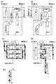
【0114】
図6には、j行i列目の画素11を示す。図6において、二点破線で囲んだ領域が画素11に相当する。点模様の領域は、ポリシリコン膜である。右上り斜線と右下り二重斜線は、それぞれ別の層の導電体膜(金属膜等)である。バツ印は層間の接触点を示す。そして、チェック模様の領域86は自発光素子84の陽極に相当する。
【0115】
第1走査線(Gaj)下には、トランジスタ71〜75、85が形成されている。第2走査線(Gbj)下には、トランジスタ76〜79が形成されている。電源線(Vi)の下に容量素子83が形成されている。
【0116】
駆動用素子を構成する3つのトランジスタ80〜82は同サイズに揃えて互いに隣接させて形成されている。このように形成することで、トランジスタを作製する段階から、同一画素内におけるトランジスタ80〜82間のバラつきが、大きくなりにくくすることはできる。本発明の構成である「並列書込み直列駆動」は、駆動用素子を構成する複数のトランジスタ間に元々存在するバラつきの影響を、さらに小さくする手法である。したがって、当初からバラつきが抑えられた複数のトランジスタを駆動用素子に用いるのであれば、本発明の効果を非常に大きく生かすことができるため好ましい。そして、自発光素子の発光輝度のバラつきは、さらに僅少となる。
【0117】
なお本発明の表示装置、発光装置を作製する工程については、例えば、特開2001−343933等を参照できる。駆動用素子を構成する複数のトランジスタは、ソースとドレインについては対称的である方が好ましい。しかしながら、複数のトランジスタのソースとドレインが対称的であることが必須ではない。
【0118】
本実施の形態は、実施の形態1〜3と任意に組み合わせることが可能である。
【0119】
(実施の形態5)
本実施の形態では、本発明の表示装置、発光装置の構成の例について図7を用いて説明する。画素内ではなく、装置の全体的な構成の例を説明する。
【0120】
本発明の表示装置、発光装置は、基板1801上に、複数の画素がマトリクス状に配置された画素部1802を有する。画素部1802の周辺部には、信号線駆動回路1803、第1の走査線駆動回路1804及び第2の走査線駆動回路1805が配置されている。信号線駆動回路1803と、第1の走査線駆動回路1804及び第2の走査線駆動回路1805には、FPC1806を介して、外部より電源や信号が供給される。
【0121】
図7(A)の例においては、信号線駆動回路1803と、走査線駆動回路1804及び1805が集積されているが、本発明はこれに限定されるものではない。例えば、第2の走査線駆動回路1805を欠いていてもよい。あるいは、信号線駆動回路1803、走査線駆動回路1804及び1805を欠いていてもよい。
【0122】
第1の走査線駆動回路1804及び第2の走査線駆動回路1805の例を、図7(B)を用いて説明する。図7(B)に示す走査線駆動回路1804及び1805は、シフトレジスタ1821、バッファ回路1822をそれぞれ有している。
【0123】
図7(B)の回路の動作を簡単に説明する。シフトレジスタ1821は、クロック信号(G−CLK)、クロック反転信号(G−CLKb)、スタートパルス信号(G−SP)に基づき、順次パルスを出力する。該パルスは、バッファ回路1822で電流増幅された後、走査線に入力される。こうして走査線は、1行ずつ順次選択状態となる。
【0124】
なお本明細書において、同期タイミングとは、クロック信号(G−CLK)、クロック反転信号(G−CLKb)、スタートパルス信号(G−SP)に基づいて出力されたパルスを指す。
【0125】
なお必要に応じ、バッファ回路1822内にレベルシフタを設置してもよい。レベルシフタにより、電圧振幅を変更することができる。
【0126】
次いで、信号線駆動回路1803の例を、図7(C)を用いて説明する。図7(C)に示す信号線駆動回路1803は、シフトレジスタ1831、第1のラッチ回路1832、第2のラッチ回路1833、電圧電流変換回路1834を有している。
【0127】
図7(C)の回路の動作を簡単に説明する。図7(C)の回路は、中間階調表示方式として、ディジタル時間階調法を採用した場合の回路である。
【0128】
シフトレジスタ1831は、クロック信号(S−CLK)、クロック反転信号(S−CLKb)、スタートパルス信号(S−SP)に基づき、順次サンプリングパルスを第1のラッチ回路1832に出力する。各列の第1のラッチ回路1832は、該パルスのタイミングに従って、ディジタルビデオ信号を順次読込む。第1のラッチ回路1832において、最終列までビデオ信号の読込みが完了すると、第2のラッチ回路1833にラッチパルスが入力される。ラッチパルスにより、各列の第1のラッチ回路1832に読込まれていたビデオ信号は、一斉に各列の第2のラッチ回路1833に転送される。第2のラッチ回路1833に転送されたビデオ信号は、電圧電流変換回路1834において、適宜形式変換処理され、画素へ転送される。ビデオ信号のうち、オンデータは電流形式に変換され、オフデータは電圧形式のまま電流増幅される。ラッチパルス後、シフトレジスタ1831、第1のラッチ回路1832は、次行のビデオ信号読込み動作として、上記動作を繰り返す。
【0129】
図7(C)の信号線駆動回路1803の構成はあくまで一例であり、アナログ階調法を採用した場合には、別の構成にする。またディジタル時間階調法を採用した場合であっても、他の構成にすることはできる。
【0130】
本実施の形態は、実施の形態1〜4と任意に組み合わせることが可能である。
【0131】
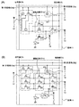
(実施の形態6)
本実施の形態では、トランジスタの特性曲線(図8)を用いて、本発明の効果について説明する。説明を簡単にするため、駆動用素子を構成するトランジスタの個数が2個の場合を例に挙げて説明する。画素回路の構成としては、図2(B)に示した通りであるとする。またここで用いるトランジスタの特性曲線は理想的なものであるとしており、実際のトランジスタの特性曲線とは若干の差異がある。例えば図8では、トランジスタのチャネル長変調はゼロとしてある。
【0132】
トランジスタのソースの電位を基準として、ゲートの電位をVg、ドレインの電位をVd、ソースドレイン間に流れる電流をIdとする。但し、トランジスタがpチャネル型のときは、正負を入れ替えるなど正負の向きは適宜設定してある。例えば、図8(A)(B)において、曲線801〜804は、ある一定のゲート電位Vg下におけるId-Vd特性曲線である。一点鎖太曲線805は、駆動用素子を構成する2個のトランジスタの一方について、ゲートとドレインを短絡することにより、VgとVdとを等しくした条件下でのId-Vd変化を示したものである。すなわち、一点鎖太曲線805には、該トランジスタ固有の電気的特性(電界効果移動度、しきい電圧値)が反映されている。同様に、二点鎖太曲線806は、駆動用素子を構成する他の一方のトランジスタについて、ゲートとドレインを短絡することにより、VgとVdとを等しくした条件下でのId-Vd変化を示したものである。
【0133】
図8(A)(B)は、駆動用素子を構成する2個のトランジスタが各々異なった電気的特性をもっている場合に、本発明の構成である「並列書込み直列駆動」により、自発光素子駆動電流がどうなるかを調べたものである。図8(A)は、2個のトランジスタ間において特に、電界効果移動度の違いが大きい場合の例である。図8(B)は、2個のトランジスタ間において特に、しきい電圧値の違いが大きい場合の例である。図8(A)(B)から、結論としては、各場合での自発光素子駆動電流は、807の三角矢印の長さで示されるとおりとなる。この理由について、以下に簡単に説明する。
【0134】
まず、トランジスタ38、39の特性曲線として、両トランジスタの特性が等しく、且つ一点鎖太曲線805が対応する場合を考える。
【0135】
データ電流書込み時には、図2(B)のトランジスタ31〜36がオンとなる。トランジスタ31〜34がオンとなることから、駆動用素子を構成する2個のトランジスタ38、39では、ゲートとドレインが短絡される。よってトランジスタ38、39の動作点は、一点鎖太曲線805上の点であり、データ電流値IWにより決まるある一点である。仮に該動作点が805と801の交点としておく。つまり、805と801の交点の縦軸値Idの2倍が、データ電流値IWであるとしておく。
【0136】
自発光素子の発光時には、図2(B)のトランジスタ31〜36がオフとなり、トランジスタ37、42がオンとなる。トランジスタ31〜34がオフとなることから、トランジスタ38、39のゲート電位は、データ電流書込み時のままで保持される。そして自発光素子の発光時には、トランジスタ39が飽和領域で動作し、トランジスタ38が非飽和領域で動作する。自発光素子の発光時における、トランジスタ38のId-Vd曲線は801で表され、トランジスタ39のId-Vd曲線は803で表される。
【0137】
図8(A)に示すグラフにおいて、各一点鎖線矢印は、長さと縦軸座標は等しい。自発光素子の発光時におけるトランジスタ38の動作点は、左側の一点鎖線矢印の右端と801との接点である。そして求めるべき自発光素子の駆動電流IEは、一点鎖線矢印の縦軸座標、すなわち、807の実線三角矢印の長さである。なお図8(B)に示すグラフでも同様であり、求めるべき自発光素子駆動電流IEは807の実線三角矢印の長さである。トランジスタ38の特性曲線とトランジスタ39の特性曲線が、いずれも等しい場合には、結果的には求めるべき自発光素子駆動電流IEは、データ電流値IWの4分の1の大きさとなる。
【0138】
次に、トランジスタ38の特性曲線として二点鎖太曲線806が対応し、トランジスタ39の特性曲線として一点鎖太曲線805が対応する場合を考える。データ電流値IWは、上で述べたトランジスタ38、39の特性曲線としていずれも805が対応する場合と、同一とする。
【0139】
データ電流書込み時には、図2(B)の駆動用素子を構成する2個のトランジスタ38、39では、ゲートとドレインが短絡される。よってトランジスタ38の動作点は二点鎖太曲線806上の点であり、トランジスタ39の動作点は一点鎖太曲線805上の点である。そして、トランジスタ38の動作点の縦軸座標と、トランジスタ39の動作点の縦軸座標との和は、データ電流値IWである。よってトランジスタ38の動作点は、806と802の交点となる。トランジスタ39の動作点は、トランジスタ38の動作点と横軸座標が等しい、曲線805上の点となる。
【0140】
自発光素子の発光時には、図2(B)のトランジスタ31〜34がオフとなることから、トランジスタ38、39のゲート電位は、データ電流書込み時のままで保持される。そして自発光素子発光時には、トランジスタ39が飽和領域で動作し、トランジスタ38が非飽和領域で動作する。自発光素子発光時における、トランジスタ38のId-Vd曲線は802で表される。
【0141】
図8(A)に示すグラフにおいて、同縦軸座標値にある各二点鎖線矢印は、長さが等しい。図8(A)において上部に位置する二点鎖線矢印の組が、トランジスタ38の特性曲線として二点鎖太曲線806が対応しており、トランジスタ39の特性曲線として一点鎖太曲線805が対応している場合である。自発光素子の発光時における、トランジスタ38の動作点は、図8(A)に示すグラフにおいて、左側に位置する該二点鎖線矢印の右端と802との接点である。そして求めるべき自発光素子駆動電流IEは、該二点鎖線矢印の縦軸座標、すなわち、807の長点線三角矢印(左側)の長さである。なお図8(B)上でも同様の事情が成立し、求めるべき自発光素子駆動電流IEは、807の長点線三角矢印(左側)の長さである。
【0142】
また別の場合として、トランジスタ38の特性曲線として一点鎖太曲線805が対応し、トランジスタ39の特性曲線として二点鎖太曲線806が対応する場合も、同様にして行うことができる。本実施の形態では詳しい説明は省略するが、図8(A)(B)とも、求めるべき自発光素子駆動電流IEは、807の長点線三角矢印(右側)の長さとなる。
【0143】
さらに別の場合として、トランジスタ38、39の特性曲線として、いずれも二点鎖太曲線805が対応する場合の検討も、同様に行うことができる。本実施の形態では詳しい説明は省略するが、図8(A)(B)とも、求めるべき自発光素子駆動電流IEは、807の短点線三角矢印の長さとなる。
【0144】
そして、図8(A)(B)における、807の三角矢印の長さから、駆動用素子を構成するトランジスタ38、39の特性バラつきが、自発光素子の駆動電流IEにどのように反映されるかの概略をみることができる。
【0145】
比較のために、図8(A)(B)には808の狭角矢印、809の広角矢印も記載してある。808の狭角矢印は、電流入力方式でカレントミラー型を用いる画素回路の場合において、上記と同様の検討を行った結果である。すなわち、カレントミラーの2つのトランジスタ間に、上記と同様の特性バラつきが存在したとき、自発光素子の駆動電流IEがどのようになるのかを示している。809の広角矢印は、電圧入力方式の画素回路の場合において、同様の検討を行った結果である。つまり、異なる画素の自発光素子駆動トランジスタ間に、上記と同様の特性バラつきが存在したとき、自発光素子駆動電流IEがどうなるかを示している。
【0146】
そして、図8(A)(B)の807の三角矢印、808の狭角矢印、809の広角矢印を比較すると、以下に示す点が理解できる。
【0147】
まず、807の三角矢印、808の狭角矢印では、同一画素内の2つのトランジスタ間にさえ特性バラつきがない限りは、トランジスタの特性曲線が805、又は806であったとしても自発光素子の駆動電流IEは一定となる。すなわち、電流入力方式でカレントミラー型を用いる画素回路でも、本発明の「並列書込み直列駆動」の画素回路でも、基板全体でトランジスタの特性を一定に揃える必要はなく、同一画素内の2つのトランジスタ間の特性バラつきさえ、抑制すれば十分である。この点は、電圧入力方式の画素回路に対して非常に優位である。
【0148】
しかし、同一画素内の二つのトランジスタ間の特性バラつきが存在すると、808の狭角矢印では、自発光素子駆動電流IEのバラつきが大きくなる。すなわち、電流入力方式でカレントミラー型を用いる画素回路では、同一画素内の二つのトランジスタ間の特性バラつきの影響が大きく現れてしまう。極端な場合では、電圧入力方式の画素回路よりも、自発光素子駆動電流IEのバラつきが大きくなることがある。この観点から考えると、本発明の「並列書込み直列駆動」の画素回路では、同一画素内の二つのトランジスタ間の特性バラつきの影響が大きく抑制されている。実際の表示装置、発光装置では、トランジスタの特性バラつきは、同一画素内よりも基板全体にわたるものの方が深刻である。したがって同一画素内の二つのトランジスタ間の特性バラつきは、本発明の「並列書込み直列駆動」の画素回路のように抑制されれば、実用上はほとんど問題がなくなる。
【0149】
本実施の形態では、駆動用素子を構成するトランジスタに個数が、2個の場合を例に、本発明の効果について説明した。しかし、駆動用素子を構成するトランジスタに個数が、3個以上の場合においても同様の事情が成立する。
【0150】
本実施の形態は、実施の形態1〜5と任意に組み合わせることが可能である。
【0151】
(実施の形態7)
本実施の形態においては、有機化合物層として高分子化合物を適用し、さらに陽極と発光層との間に導電性高分子化合物からなるバッファ層を設けた自発光素子において、直流駆動(常に順方向バイアスを印加)と、交流駆動(順方向バイアスと逆方向バイアスを一定周期で交互に印加)を行った際の輝度劣化について測定を行った結果について述べる。
【0152】
図13(A)(B)は、順方向バイアス:3.7V、逆方向バイアス:1.7V、デューティ50%、交流周波数60Hzにおいて交流駆動を行った際の信頼性試験の結果を示している。初期輝度は約400cd/cm2であった。比較用に、直流駆動(順方向バイアス:3.65V)を行った際の信頼性試験の結果も同時に示した。その結果、直流駆動においては、400時間程度で輝度が半減したのに対し、交流駆動においては、約700時間経過後も、半減には至らなかった。
【0153】
図13(C)(D)は、順方向バイアス:3.8V、逆方向バイアス:1.7V、デューティ50%、交流周波数600Hzにおいて交流駆動を行った際の信頼性試験の結果を示している。初期輝度は約300cd/cm2であった。比較用に、直流駆動(順方向バイアス:3.65V)を行ったさいの信頼性試験の結果も同時に示した。結果、直流駆動においては、500時間程度で輝度が半減したのに対し、交流駆動においては、約700時間経過後も、初期輝度の60%程度を保持していた。
【0154】
以上の結果より、交流駆動を行った自発光素子は、直流駆動を行った自発光素子よりも信頼性が高いことが分かる。
【0155】
(実施の形態8)
本実施の形態では、本発明の発光装置の断面構造について、図14を用いて簡単に説明する。なお説明を簡単にするために、図14には駆動用TFT507と発光素子の断面構造のみを図示する。
【0156】
図14において、500は絶縁表面を有する基板である。基板500上には、駆動用TFT507が設けられている。そして、駆動用TFT507が有する活性層に設けられた不純物領域に接続するように配線が設けられ、前記配線と接続するように画素電極509が設けられている。画素電極509上には有機導電体膜522が設けられ、該有機導電体膜522上には有機薄膜(発光層)523が設けられている。有機薄膜(発光層)523上には、対向電極524が設けられている。
【0157】
そして、画素電極509、有機導電体膜522、有機薄膜(発光層)523及び対向電極524との積層体が発光素子に相当する。発光素子から発せられる光は、基板500に向かって発せられる場合と、基板500と反対方向に発せられる場合がある。前者は下面出射と称され、後者は上面出射と称されており、下面出射の場合は、画素電極509が陽極に相当し対向電極524が陰極に相当する。また上面出射の場合は、画素電極509が陰極に相当し対向電極524が陽極に相当する。
【0158】
なお有機薄膜(発光層)523には、赤、青、緑、白等の光を発する材料を適宜用いることが出来る。そして、白色の光を発する材料を用いて有機薄膜(発光層)523を構成するときには、画素電極509又は対向電極524を透明導電膜で形成し、それに対向する面にカラーフィルターの着色層を配置するとよい。そうすると、白色の材料を用いてもカラー表示を実現することが出来る。
【0159】
(実施の形態9)
本実施の形態では、本発明の表示装置、発光装置を搭載した電子機器等を、いくつか例示する。
【0160】
本発明の表示装置、発光装置を搭載した電子機器として、モニター、ビデオカメラ、ディジタルカメラ、ゴーグル型ディスプレイ(ヘッドマウントディスプレイ)、ナビゲーションシステム、音響再生装置(オーディオコンポ、カーオーディオ等)、ノート型パーソナルコンピュータ、ゲーム機器、携帯情報端末(モバイルコンピュータ、携帯電話、携帯型ゲーム機または電子書籍等)、記録媒体を備えた画像再生装置(具体的にはDigital Versatile Disc(DVD)等の記録媒体を再生し、その画像を表示しうるディスプレイを備えた装置)などが挙げられる。特に、斜め方向から画面を見る機会が多い電子機器については、視野角の広さが重要視されるため、発光装置を用いることが望ましい。それら電子機器の具体例を図9に示す。
【0161】
図9(A)はモニターである。図9(A)に示すモニターは筐体2001、支持台2002、表示部2003、スピーカー部2004、ビデオ入力端子2005等を有する。本発明の表示装置、発光装置は表示部2003に用いることができる。なおモニターには、パソコン用、TV放送受信用、広告表示用などのすべての情報表示装置が含まれる。
【0162】
図9(B)はディジタルスチルカメラである。図9(B)に示すディジタルスチルカメラは、本体2101、表示部2102、受像部2103、操作キー2104、外部接続ポート2105、シャッター2106等を含んでいる。本発明の表示装置、発光装置は表示部2102に用いることができる。
【0163】
図9(C)はノート型パーソナルコンピュータである。図9(C)に示すノート型パーソナルコンピュータは、本体2201、筐体2202、表示部2203、キーボード2204、外部接続ポート2205、ポインティングマウス2206等を含んでいる。本発明の表示装置、発光装置は表示部2203に用いることができる。
【0164】
図9(D)はモバイルコンピュータである。図9(D)に示すモバイルコンピュータは、本体2301、表示部2302、スイッチ2303、操作キー2304、赤外線ポート2305等を含んでいる。本発明の表示装置、発光装置は表示部2302に用いることができる。
【0165】
図9(E)は記録媒体を備えた携帯型の画像再生装置(具体的にはDVD再生装置)である。図9(E)に示すDVD再生装置は、本体2401、筐体2402、表示部A2403、表示部B2404、記録媒体(DVD等)読込み部2405、操作キー2406、スピーカー部2407等を含んでいる。本発明の表示装置、発光装置は、表示部A2403、表示部B2404に用いることができる。なお、記録媒体を備えた画像再生装置には家庭用ゲーム機器なども含まれる。
【0166】
図9(F)はゴーグル型ディスプレイ(ヘッドマウントディスプレイ)である。図9(F)に示すディスプレイは、本体2501、表示部2502、アーム部2503等を含んでいる。本発明の表示装置、発光装置は表示部2502に用いることができる。
【0167】
図9(G)はビデオカメラである。図9(G)に示すビデオカメラは、本体2601、表示部2602、筐体2603、外部接続ポート2604、リモコン受信部2605、受像部2606、バッテリー2607、音声入力部2608、操作キー2609等を含んでいる。本発明の表示装置、発光装置は表示部2602に用いることができる。
【0168】
図9(H)は携帯電話である。図9(H)に示す携帯電話は、本体2701、筐体2702、表示部2703、音声入力部2704、音声出力部2705、操作キー2706、外部接続ポート2707、アンテナ2708等を含んでいる。本発明の表示装置、発光装置は表示部2703に用いることができる。なお、表示部2703は黒色背景に白色文字を表示することで、携帯電話の消費電力を抑制することができる。
【0169】
将来に自発光素子の発光輝度を安定的に高くすることが可能となれば、本発明の表示装置、発光装置から出力した画像情報を含む光をレンズ等で拡大投影して、フロント型又はリア型のプロジェクターに用いることもできる。
【0170】
このように、本発明の適用範囲は極めて広く、あらゆる分野の電子機器等に使用することが可能である。
【0171】
【発明の効果】
本発明はAM型表示装置、発光装置において、各画素に設置される駆動用素子を複数のトランジスタにより構成する。その上で、画素にデータ電流を読込むときには該複数のトランジスタを並列接続状態にし、自発光素子を発光させるときには該複数のトランジスタを直列接続状態にする。このように、駆動用素子を構成する複数のトランジスタの接続状態を、並列または直列と適宜切替えることを特徴とする。その結果、次のような効果が生じる。
【0172】
まず、同一画素内の駆動用素子を構成する複数のトランジスタさえ、バラつきがなければ、表示画面全体で発光輝度のムラが現れてしまうという、表示品位上の重大な欠陥を回避することができる。すなわち、各画素に設置されるトランジスタの電気的特性は、基板全体にわたって観察すると、かなりのバラつきをもつ。このバラつきが自発光素子の駆動電流IEに反映されて、表示画面全体で発光輝度のムラとなってしまうのを防止することができる。ただし、図10(A)のようなカレントミラーを用いた画素回路の場合においても、同一画素内のカレントミラーの二つのトランジスタさえバラつきがなければ、表示画面全体で発光輝度のムラとなるのを防止することができる。この点で本発明は、図10(A)のようなカレントミラーを用いた画素回路の場合と同様の効果を有する。
【0173】
しかし、図10(A)のようなカレントミラーを用いた画素回路の場合、同一画素内のカレントミラーの2つのトランジスタ間にバラつきが存在してしまうと、結局発光輝度が画素間で異なってしまうのを防止することができなくなる。その点、本発明の場合では、同一画素内の駆動用素子を構成する複数のトランジスタ間にバラつきが存在しても、その影響は小さく抑制されるため、実用上問題となるほど画素間で発光輝度がバラついてしまうことは防止することができる。
【0174】
また、図10(B)のような画素回路の場合、画素間で発光輝度がバラついてしまうのを防止することができる。しかしながら、図10(B)の画素回路の場合には、画素に書込むデータ電流IWと、自発光素子を発光させるときの自発光素子の駆動電流IEとの比が、同一値でなくてはならない。これは実用上、非常に厳しい制限である。本発明の場合では、駆動用素子を構成するトランジスタを複数に分割するため、画素に書込むデータ電流IWを自発光素子駆動電流IEよりも大きくすることが可能である。
【0175】
本発明は以上のような利点を有することから、実用的なAM型表示装置、発光装置を製造する上で、重要な技術である。
【0176】
また図13の測定結果より、交流駆動を行った自発光素子は、直流駆動を行った自発光素子よりも信頼性が高いことが分かる。そこで本発明は、フレーム期間の所定の期間において交流駆動を行うことによって、自発光素子の信頼性が改善された表示装置、発光装置を提供する。
【図面の簡単な説明】
【図1】 本発明の表示装置、発光装置の画素を示す図。
【図2】 本発明の表示装置、発光装置の画素を示す図。
【図3】 本発明の表示装置、発光装置の画素を示す図。
【図4】 本発明の表示装置、発光装置の画素を示す図。
【図5】 本発明の表示装置、発光装置の画素における電流の経路を示す図。
【図6】 本発明の表示装置、発光装置の画素の平面レイアウトを示す図。
【図7】 本発明の表示装置、発光装置を示す図。
【図8】 駆動用素子を構成するトランジスタの特性を示す図。
【図9】 本発明の表示装置、発光装置を適用した電子機器を示す図。
【図10】 公知の表示装置、発光装置の画素を示す図。
【図11】 本発明の表示装置、発光装置の画素を示す図。
【図12】 本発明の表示装置、発光装置の画素を示す図。
【図13】 自発光素子の輝度と時間の関係を示す図。
【図14】 本発明の表示装置、発光装置の断面構造を示す図。[0001]
BACKGROUND OF THE INVENTION
The present invention relates to a technology of a light emitting device and a display device. Furthermore, the present invention relates to an electronic device equipped with the light emitting device or the display device. The light-emitting device in this specification refers to a device that uses light emitted from a self-luminous element. Examples of the self-light emitting element include an organic light emitting diode (OLED) element, an inorganic material light emitting diode element, and a field emission light emitting element (FED element). The display device in this specification refers to a device that arranges a plurality of pixels in a matrix and visually transmits image information, a so-called display.
[0002]
[Prior art]
In recent years, the importance of display devices that display images has increased. As a display device, a liquid crystal display device that displays an image using a liquid crystal element is widely used as a display device for various applications including a mobile phone and a personal computer, taking advantage of high image quality, thinness, and light weight. It has been.
[0003]
On the other hand, development of display devices and light-emitting devices using self-luminous elements is also underway. There are various types of self-luminous elements such as organic materials, inorganic materials, thin film materials, bulk materials, and dispersion materials.
[0004]
Among the above self-luminous elements, organic light emitting diode (OLED) elements are promising in the future for display devices. OLED display devices that use OLED elements as self-luminous elements have features such as high response speed, high viewing angle, and low voltage drive suitable for video display, in addition to features that are thinner and lighter than existing liquid crystal display devices. Therefore, a wide range of applications such as mobile phones and personal digital assistants (PDAs), televisions and monitors are expected. As a result, OLED display devices are attracting attention as next-generation displays.
[0005]
In particular, an active matrix (hereinafter referred to as AM) type OLED display device is capable of high-definition and large-screen display, which is difficult with a passive matrix (hereinafter referred to as PM) type. Expectations for practical use are very strong because of its low power consumption and high reliability.
[0006]
The OLED element has a structure having an anode, a cathode, and an organic compound layer sandwiched between the anode and the cathode. The amount of current flowing through the OLED element and the light emission luminance of the OLED element are generally proportional. In a pixel included in an AM type OLED display device, a driving transistor for controlling the light emission luminance of the OLED element of the pixel is often connected in series to the OLED element.
[0007]
By the way, driving methods for displaying an image in an AM type OLED display device are roughly classified into a voltage input method and a current input method. In the former voltage input method, a video signal of voltage value format data is input as a video signal input to a pixel. In the latter current input method, a video signal of current value format data is input as a video signal input to the pixel.
[0008]
In the voltage input method, the voltage of the video signal is directly applied to the gate electrode of the driving transistor of the normal pixel. Therefore, when the OLED element emits light at a constant current, if the electric characteristics of the driving transistor are not uniform among the pixels, the OLED element driving current of each pixel varies. The variation in the OLED element driving current is a variation in the light emission luminance of the OLED element. That is, the variation in the light emission luminance of the OLED element is a sandstorm-like or carpet-like unevenness on the entire screen, and degrades the quality of the display image.
[0009]
Therefore, there is a current input method as one of effective means for suppressing variations in the OLED element driving current in the voltage input method. In the current input method, a data current value of a normal video signal is stored, and a current that is the same as the stored current value or several times (a positive real number including less than 1) is supplied as an OLED element driving current.
[0010]
A typical example of a pixel circuit of a current input type AM-type OLED display device is shown in FIG. 10A (see A. Yumoto et al., Proc. Asia Display / IDW '01 pp1395-1398 (2001), etc.) ). In FIG. 10A,
[0011]
Next, FIG. 10B shows an example of a pixel circuit of an AM type OLED display device of a current input system different from that in FIG. 10A (IM Hunter et al., Proc. AM-LCD 2000 pp249-252 (2000 ) Etc.). In FIG. 10B,
[0012]
[Problems to be solved by the invention]
The pixels shown in FIGS. 10A and 10B should be able to store the data current value accurately as described above, but have the following serious problems.
[0013]
First, the problem with the pixel circuit of FIG. 10A is that it is a precondition that the two transistors constituting the current mirror have the same electrical characteristics. If a device is devised at the time of designing the pixel circuit, both transistors can be manufactured next to each other on the substrate, so that variations can be reduced to some extent. However, a transistor made of polysilicon still has a variation exceeding the allowable limit in the electrical characteristics such as the threshold voltage of the TFT and the field effect mobility due to defects at the grain boundaries. End up.
[0014]
Here, a case where a 64 gradation image is displayed will be described as an example. When displaying an image with 64 gradations, it is necessary to suppress the variation in luminance of the self-luminous element to about 1% or less. However, in the pixel circuit of FIG. 10A, it is difficult to store the data current value with an accuracy of 1% in the polysilicon that is normally used at present. That is, only by using the pixel circuit of FIG. 10A, there is no unevenness on the entire screen, and a sufficiently uniform high-quality display image cannot be obtained.
[0015]
Next, the problem in the pixel circuit of FIG. 10B is that the video signal data current written to the pixel and the OLED element driving current when the OLED element emits light have the same value. When an AM type OLED display device is manufactured, the fact that both currents must have the same value is a practically severe restriction.
[0016]
This is because in the AM type OLED display device, a large amount of parasitic capacitance and parasitic resistance are attached to signal lines and the like. If a large amount of parasitic capacitance and parasitic resistance are attached, it is often necessary to take measures to make the video signal data current larger than the OLED element driving current. In particular, when the video signal data current is expressed in grayscale with an analog value, it becomes very difficult to write the video signal data current in the dark part.
[0017]
The present invention has been made in view of the above problems. First, the present invention differs from the pixel circuit of FIG. 10B in that the ratio of the video signal data current written to the pixel and the OLED element driving current when the OLED element emits light is not fixed to “1”. It is an object to provide an OLED display device. Next, unlike the pixel circuit of FIG. 10A, the present invention is based on the premise that some variation in electrical characteristics still remains between adjacent transistors in the same pixel. In addition, the present invention provides an AM type OLED display device in which variation in OLED element driving current is sufficiently suppressed as compared with a pixel circuit using a current mirror as shown in FIG. Is an issue.
[0018]
In addition, the self-luminous element has a problem of low reliability and the like caused by deterioration of the organic compound layer. Therefore, an object of the present invention is to provide a display device and a light-emitting device in which the problem of reliability of the self-light-emitting element is improved.
[0019]
[Means for Solving the Problems]
In order to solve the above problems, according to the present invention, in an AM display device or a light emitting device, a driving element installed in each pixel is configured by a plurality of transistors, and when the data current is read into the pixel, the plurality of transistors are arranged. When the self-light-emitting elements are caused to emit light in parallel connection, the plurality of transistors are connected in series.
[0020]
Note that even in the case of a display device or a light-emitting device using an element other than an OLED element, the configuration of the present invention can be used when a current-driven element is used.
[0021]
In order to solve the above problems, the present invention is characterized in that a drive voltage (reverse bias voltage) having a polarity opposite to that during light emission is applied to the light emitting element at regular intervals. This utilizes the fact that, when a drive voltage having a reverse polarity is applied to a light emitting element, the variation in current-voltage characteristics of the light emitting element is improved.
[0022]
The present invention includes a self-luminous element having first and second electrodes;
A light-emitting device provided with a pixel provided with driving means having n transistors (n is a natural number of 2 or more) to which each gate electrode is connected in common,
Corresponding to the synchronization timing of the video signal input to the pixel, the sources and drains of the n transistors are connected in series, and the current I W In response to the video signal, the sources and drains of the n transistors are connected in parallel, and a current I is supplied to the self-luminous element. E Setting means to flow,
Supply means for supplying a reverse bias voltage to the self-luminous element by changing the potential of the first or second electrode for a predetermined period of a unit frame period corresponding to the synchronization timing of the video signal It is characterized by having.
[0023]
The present invention includes a self-luminous element having first and second electrodes;
A light-emitting device provided with a pixel provided with driving means having n transistors (n is a natural number of 2 or more) to which each gate electrode is connected in common,
Corresponding to the synchronization timing of the video signal input to the pixel, the current I is connected between the sources and drains of the n transistors in series. W In response to the video signal, the sources and drains of the n transistors are connected in parallel, and a current I is supplied to the self-luminous element. E Setting means to flow,
Erasing that stops the light emission of each of the self light emitting elements when the light emission period of each of the self light emitting elements reaches a predetermined light emission period with respect to a predetermined period of a unit frame period corresponding to the synchronization timing of the video signal Means,
Supply means for supplying a reverse bias voltage to the self-luminous element by changing the potential of the first or second electrode with respect to a predetermined period of the frame period.
[0024]
The setting means corresponds to a transistor that controls input of a video signal to a pixel, and more specifically corresponds to the
Further, the driving means corresponds to a driving transistor in the pixel. The driving transistor has a role of driving the self-luminous element, and in many cases, refers to a transistor directly connected to the self-luminous element.
Finally, the erasing means has a function of stopping the light emission of the self-luminous element, and specifically corresponds to the
[0025]
Here, an outline of a pixel structure of the display device or the light-emitting device of the present invention will be described with reference to FIGS. FIG. 1A illustrates a pixel 11 arranged in the jth row and the ith column in a pixel portion having a plurality of pixels. The pixel 11 includes a signal line (Si), a power supply line (Vi), a first scanning line (Gaj), a
[0026]
The first or second electrode of the self-light-emitting
[0027]
Since the self-emitting element typically corresponds to an OLED element, a diode symbol is used as a symbol representing the self-emitting element in this specification. However, the diode characteristics are not essential for the self-luminous elements, and the present invention is not limited to the self-luminous elements having the diode characteristics. Further, the self-light-emitting element in this specification may be a current-driven display element, and does not need to bear a display function by self-light emission. For example, an element that serves as an optical shutter, such as liquid crystal, and is controlled by a current value instead of a voltage value is also included in the self-luminous element in this specification.
[0028]
For the
[0029]
The
[0030]
FIG. 1B shows a case where a
[0031]
The
[0032]
In the present invention, the driving element 15 is composed of a plurality of transistors, and when the data current of the video signal is written into the pixel 11 and when the current is caused to flow through the self-light-emitting
[0033]
As an example, the pixel 11 in the case where the driving element 15 includes four
[0034]
FIG. 1C shows a case where a data current is written to the pixel 11, and FIG. 1D shows a case where a self-luminous element emits light. 1C and 1D, the
[0035]
First, a case where a data current is written to the pixel 11 will be described. In FIG. 1C, the
[0036]
Next, a case where the self
[0037]
Finally, a case where a reverse bias is applied to the self-light-emitting
[0038]
In FIG. 1E, a reverse bias can be applied to the light-emitting
[0039]
As described above, according to the present invention, when writing a data current to a pixel, the
[0040]
[Expression 1]
I W = N 2 × I E ... (1)
[0041]
In order for Expression (1) to be strictly established, it is a condition that all the transistors constituting the driving element 15 have the same electrical characteristics. However, even if the electrical characteristics of the transistor are slightly different from each other, it is practically possible to treat that the expression (1) is approximately established.
[0042]
Therefore, in the present invention, the driving element 15 is composed of a plurality of transistors, and when the video signal current is written to the pixel 11 and the self-light emitting element emits light, the connection of the plurality of transistors is connected in parallel and in series. By switching to, current value I at the time of writing W And the current value I when driving the self-luminous element E And can be set arbitrarily.
[0043]
As another feature of the present invention, even if the electrical characteristics of the transistors constituting the driving element 15 are slightly different from each other, the influence of the self-luminous element driving current I E There is a point that can greatly reduce the reflection. This will be described in Embodiment 5 with a specific example.
[0044]
Further, in the pixel circuit using the current mirror as shown in FIG. 10A, there is a problem that it is required to have the same electrical characteristics as far as two transistors in the pixel are concerned. However, in the present invention, it is already premised that even the transistors in the same pixel have slightly different electrical characteristics. That is, the present invention is superior to a pixel circuit using a current input type current mirror in terms of tolerance to variations in transistor characteristics. As a result, the present invention provides a self-luminous element driving current I even if there is a variation in the electrical characteristics of the polysilicon TFT due to defects at the crystal grain boundaries. E Can be made uniform to a practical level.
[0045]
DETAILED DESCRIPTION OF THE INVENTION
(Embodiment 1)
The outline of the pixel of the display device and the light emitting device of the present invention has been described with reference to FIG. In
[0046]
A first example will be described with reference to FIG.
[0047]
FIG. 2A shows the pixel 11 arranged in the j-th row and the i-th column. The pixel 11 includes a signal line (Si), a power supply line (Vi), a scanning line (Gaj), transistors 21 to 26, a capacitor element 27, and a self-
[0048]
Each gate electrode of the transistors 21 to 24 is connected to a scanning line (Gaj). The capacitor element 27 plays a role of holding a gate-source voltage of the
[0049]
When a video signal data current is written to the pixel 11 shown in FIG. 2A, a low potential signal is sent to the scanning line (Gaj), the transistors 21 to 23 are turned on, and the
[0050]
In the example of FIG. 2A, switching of the connection relationship of the
[0051]
Next, an example different from FIG. 2A will be described with reference to FIG.
[0052]
FIG. 2B shows the pixel 11 arranged in the j-th row and the i-th column. The pixel 11 includes a signal line (Si), a power supply line (Vi), a first scanning line (Gaj), a second scanning line (Gbj), transistors 31 to 39 and 42, a
[0053]
Each gate electrode of the transistors 31 to 34 is connected to the first scanning line (Gaj). The gate electrodes of the
[0054]
When a video signal data current is written to the pixel 11 shown in FIG. 2B, a low potential signal is sent to the first scanning line (Gaj) and the second scanning line (Gbj), and the transistors 31 to 36 are turned on. 37 and 42 are turned off. At this time, the
[0055]
In the example of FIG. 2B, switching of the connection relationship of the
[0056]
This is a very important feature when the intermediate gradation expression is expressed by the time gradation method. When the time gray scale method is applied to an AM type OLED display device having a drive circuit formed of a polysilicon TFT, a sufficient number can be obtained without means for stopping light emission of the self-light emitting element during the column scanning period. This is because gradation display is difficult. In addition, even when halftone expression is expressed by using analog video signal data current, it is useful for applications such as impulse-type light emission to prevent moving picture blurring peculiar to the hold type display. (Refer to, for example, T. Kurita, Proc. AM-LCD 2000 pp1-4 (2000) etc. for moving image blur peculiar to the hold type display).
[0057]
Another feature of the example of FIG. 2B is that the video signal data current can be stored more accurately. In the example of FIG. 2A, the
[0058]
Next, a third example will be described with reference to FIG.
[0059]
FIG. 3A shows the pixel 11 arranged in the j-th row and the i-th column. The pixel 11 includes a signal line (Si), a power supply line (Vi), a first scanning line (Gaj), a second scanning line (Gbj), transistors 51 to 57 and 60, a
[0060]
Each gate electrode of the transistors 51 to 55 is connected to the first scanning line (Gaj). The gate electrode of the
[0061]
When a video signal data current is written to the pixel 11 shown in FIG. 3A, a high potential signal is sent to the first scanning line (Gaj), the transistors 51 to 54 are turned on, and the transistor 55 is turned off. At this time, the
[0062]
During the above period, a low potential signal is sent to the second scanning line (Gbj), and the
[0063]
In the pixel 11 shown in FIG. 3A as well, as in the case of the example of FIG. 2B, the light emission time of the self-
[0064]
In the pixel 11 shown in FIG. 3A, the feature that the light emission time of the self-
[0065]
In the pixel 11 shown in FIG.
[0066]
Next, a fourth example will be described with reference to FIG.
[0067]
FIG. 3B shows the pixel 11 arranged in the j-th row and the i-th column. The pixel 11 includes a signal line (Si), a power supply line (Vi), a first scanning line (Gaj), a second scanning line (Gbj), transistors 71 to 82, 85, a
[0068]
The gate electrodes of the transistors 71 to 75 and 85 are connected to the first scanning line (Gaj). The gate electrodes of the transistors 76 to 79 are connected to the second scanning line (Gbj). The
[0069]
When a video signal data current is written to the pixel 11 shown in FIG. 3B, a low potential signal is sent to the first scanning line (Gaj) and the second scanning line (Gbj), and the transistors 71 to 78 are turned on. 79 and 85 are turned off. At this time, the
[0070]
In the example of FIG. 3B, switching of the connection relationship of the
[0071]
Therefore, the pixel 11 shown in FIG. 3B also has the following features resulting from the fact that the light emission time of the self-
[0072]
A fifth example will be described with reference to FIG.
[0073]
FIG. 4A shows the pixel 11 arranged in the j-th row and the i-th column. The pixel 11 includes a signal line (Si), a power supply line (Vi), a first scanning line (Gaj), a second scanning line (Gbj), transistors 91 to 103 and 106, a
[0074]
Each gate electrode of the transistors 91 to 94 is connected to the first scanning line (Gaj). The gate electrodes of the
[0075]
When a video signal data current is written to the pixel 11 shown in FIG. 4A, a low potential signal is sent to the first scanning line (Gaj) and the second scanning line (Gbj), and the transistors 91 to 98 are turned on. 99 and 106 are turned off. At this time, the
[0076]
In the example of FIG. 4A, switching of the connection relationship of the
[0077]
Therefore, the pixel 11 shown in FIG. 4A also has the following features resulting from the fact that the light emission time of the self
[0078]
A sixth example will be described with reference to FIG.
[0079]
FIG. 4B shows the pixel 11 arranged in the j-th row and the i-th column. The pixel 11 includes a signal line (Si), a power supply line (Vi), a first scanning line (Gaj), a second scanning line (Gbj),
[0080]
Each gate electrode of the
[0081]
When a video signal data current is written to the pixel 11 shown in FIG. 4B, a high potential signal is sent to the first scanning line (Gaj), the
[0082]
During the above period, a low potential signal is sent to the second scanning line (Gbj), and the
[0083]
In the pixel 11 shown in FIG. 4B as well, as in the case of the example of FIG. 2B, the light emission time of the self-light
[0084]
In the pixel 11 shown in FIG. 4B, the feature that the light emission time of the self-light-emitting
[0085]
As described above, as an example of the pixel 11 of the display device and the light emitting device of the present invention, the six types of pixels 11 having different configurations have been described with reference to FIGS. However, the pixel configuration of the display device and the light emitting device of the present invention is not limited to these six types.
[0086]
(Embodiment 2)
In this embodiment, a method for driving the pixel 11 will be described. The case of the pixel 11 shown in FIG. 4B will be described as an example with reference to FIG.
[0087]
First, the video signal writing operation and the light emitting operation will be described.
[0088]
First, the first scanning line (Gaj) in the j-th row is selected by a signal output from a scanning line driving circuit (not shown) provided around the pixel 11. That is, a low potential (L level) signal is output to the first scanning line (Gaj), and the gate electrodes of the
[0089]
When the
[0090]
Current I flowing through four diodes in parallel W Is in a steady state, the first scanning line (Gaj) is set to a high potential (H level). Then, the
[0091]
Subsequently, when the first scanning line (Gaj) becomes a high potential (H level), the p-
[0092]
In the present embodiment, since the driving element is composed of four transistors, the constant current I E Is the video signal data current I W It is about 1/16 of the size. More generally, when the driving element is composed of n transistors, the current I E Is the video signal data current I W About n 2 It becomes the size of 1 /.
[0093]
In the present embodiment, the write data current I W Drive current I of the self-luminous element E The value can be about 16 times as large as. Therefore, the self-luminous element drive current I E Even if it is difficult to directly write such a minute current directly to the pixel, the video signal data current I W Can be written to the pixel.
[0094]
In the present embodiment, an analog video system or a digital video system may be employed as a method for expressing halftones. In the case of the analog video system, the data current I that changes in an analog manner is used as the video signal data current. W Is used. In the case of the digital video system, one data current I W Unit luminance is prepared using only the on-current as a reference. Then, it is convenient to use a time gray scale method in which unit luminance is expressed by adding time in terms of time (also referred to as digital time gray scale method). Alternatively, the digital video system can also be performed by an area gradation method in which unit luminance is expressed by adding area in terms of area, or a method in which a time gradation method and an area gradation method are combined.
[0095]
In this embodiment, the video signal data current I can be obtained regardless of whether the analog video system or the digital video system is adopted. W May be required to be 0. However, the video signal data current I W When 0 is set to 0, it means that the light emission luminance of the self-luminous element is set to 0. W Does not need to be accurately written and stored in the pixel. Therefore, in such a case, a gate voltage that turns off the
[0096]
Next, the light emission stop operation will be described.
[0097]
First, the second scanning line (Gbj) in the j-th row is selected by a signal output from another scanning line driving circuit (not shown) provided around the pixel 11. That is, a low potential (L level) signal is output to the second scanning line (Gbj). The p-
[0098]
Then, the source and gate of the
[0099]
By using such a light emission stop operation, it is possible to arbitrarily control the light emission time of the self
[0100]
Finally, an operation for applying a reverse bias to the self-light-emitting
[0101]
When applying a reverse bias to the self-light
[0102]
This embodiment mode can be arbitrarily combined with
[0103]
(Embodiment 3)
In the present embodiment, a case where a new semiconductor element is disposed in order to apply a reverse bias voltage to the self-light-emitting
[0104]
A pixel 11 illustrated in FIG. 11A has a structure in which a
[0105]
An operation when a reverse bias is applied to the pixel 11 shown in FIGS. 11A and 11B will be described with reference to FIG. Switch 19 via the third scanning line (Gcj) b Is input to the
[0106]
[0107]
Next, the case where the structure of this embodiment is applied to the pixel 11 illustrated in FIGS. 4 and 5 will be described with reference to FIGS.
[0108]
In the pixel 11 illustrated in FIG. 12, a transistor 125, a power supply line (Vai), and a third scanning line (Gcj) are newly provided in the pixel 11 illustrated in FIGS. A detailed description of the configuration of the pixel 11 illustrated in FIG. 12 is the same as the description of the configuration of the pixel 11 illustrated in FIGS.
[0109]
Then, the operation of the pixel 11 shown in FIG. 12 will be described. Since the video signal writing operation, the light emission operation, and the light emission stop operation are in accordance with the second embodiment described above, description thereof is omitted in this embodiment. In this embodiment, only the operation of applying a reverse bias will be described.
[0110]
In the operation of applying the reverse bias, first, when the transistor 125 is turned on by a signal input through the third scanning line (Gcj), the self-light
[0111]
Note that the operation for applying the reverse bias may be performed in a period in which the light-emitting
[0112]
This embodiment can be arbitrarily combined with
[0113]
(Embodiment 4)
In this embodiment, an example of a planar layout (top view) of pixels in a display device and a light-emitting device of the present invention is presented. As the pixel circuit of this embodiment, the pixel circuit illustrated in FIG. 3B is described as an example.
[0114]
FIG. 6 shows the pixel 11 in the j-th row and the i-th column. In FIG. 6, a region surrounded by a two-dot broken line corresponds to the pixel 11. The dotted pattern region is a polysilicon film. The upper right diagonal line and the right downward double diagonal line are conductor films (metal films, etc.) in different layers. A cross mark indicates a contact point between layers. The
[0115]
Transistors 71 to 75 and 85 are formed under the first scanning line (Gaj). Transistors 76 to 79 are formed under the second scanning line (Gbj). A
[0116]
The three
[0117]
For a process for manufacturing the display device and the light-emitting device of the present invention, for example, JP-A-2001-343933 can be referred to. The plurality of transistors constituting the driving element are preferably symmetrical with respect to the source and drain. However, it is not essential that the sources and drains of the plurality of transistors be symmetric.
[0118]
This embodiment can be arbitrarily combined with
[0119]
(Embodiment 5)
In this embodiment, structural examples of the display device and the light-emitting device of the present invention will be described with reference to FIGS. An example of the overall configuration of the apparatus, not within the pixel, will be described.
[0120]
The display device and the light-emitting device of the present invention each include a pixel portion 1802 in which a plurality of pixels are arranged in a matrix on a
[0121]
In the example of FIG. 7A, the signal line driver circuit 1803 and the scanning
[0122]
Examples of the first scan
[0123]
The operation of the circuit in FIG. 7B will be briefly described. The
[0124]
Note that in this specification, the synchronization timing refers to a pulse output based on a clock signal (G-CLK), a clock inversion signal (G-CLKb), and a start pulse signal (G-SP).
[0125]
Note that a level shifter may be provided in the
[0126]
Next, an example of the signal line driver circuit 1803 is described with reference to FIG. A signal line driver circuit 1803 illustrated in FIG. 7C includes a shift register 1831, a
[0127]
The operation of the circuit in FIG. 7C will be briefly described. The circuit in FIG. 7C is a circuit in the case where a digital time gray scale method is adopted as an intermediate gray scale display method.
[0128]
The shift register 1831 sequentially outputs sampling pulses to the
[0129]
The structure of the signal line driver circuit 1803 in FIG. 7C is merely an example, and when the analog gray scale method is employed, another structure is employed. Even when the digital time gray scale method is adopted, other configurations can be used.
[0130]
This embodiment can be arbitrarily combined with
[0131]
(Embodiment 6)
In this embodiment mode, effects of the present invention are described with reference to a characteristic curve of a transistor (FIG. 8). In order to simplify the description, a case where the number of transistors constituting the driving element is two will be described as an example. The configuration of the pixel circuit is as shown in FIG. Further, the characteristic curve of the transistor used here is ideal, and is slightly different from the actual characteristic curve of the transistor. For example, in FIG. 8, the channel length modulation of the transistor is zero.
[0132]
The gate potential is set to V with reference to the transistor source potential. g , Drain potential to V d Current flowing between source and drain is I d And However, when the transistor is a p-channel transistor, the positive / negative direction is appropriately set, for example, by switching the positive / negative. For example, in FIGS. 8A and 8B, curves 801 to 804 indicate a certain gate potential V. g I below d -V d It is a characteristic curve. A one-dot chain
[0133]
FIGS. 8A and 8B show that when the two transistors constituting the driving element have different electrical characteristics, the self-light emitting element driving is performed by the “parallel writing serial driving” which is the configuration of the present invention. This is a study of what happens to the current. FIG. 8A illustrates an example in which the difference in field-effect mobility is particularly large between two transistors. FIG. 8B shows an example in which the difference in threshold voltage value is particularly large between two transistors. 8A and 8B, as a conclusion, the self-luminous element driving current in each case is as indicated by the length of the
[0134]
First, let us consider a case where the characteristics of the
[0135]
When data current is written, the transistors 31 to 36 in FIG. 2B are turned on. Since the transistors 31 to 34 are turned on, the gates and drains of the two
[0136]
When the light emitting element emits light, the transistors 31 to 36 in FIG. 2B are turned off and the
[0137]
In the graph shown in FIG. 8A, each one-dot chain line arrow has the same length and the same vertical axis coordinate. The operating point of the
[0138]
Next, consider a case where a two-dot chain
[0139]
At the time of writing data current, the gate and the drain are short-circuited in the two
[0140]
When the light emitting element emits light, the transistors 31 to 34 in FIG. 2B are turned off, so that the gate potentials of the
[0141]
In the graph shown in FIG. 8A, the two-dot chain arrows on the same vertical axis coordinate value have the same length. A pair of two-dot chain arrows positioned at the top in FIG. 8A corresponds to the two-dot chain
[0142]
In another case, the same can be done in the case where the one-dot chain
[0143]
As another case, the case where the two-dot chain
[0144]
8A and 8B, the characteristic variation of the
[0145]
For comparison, FIGS. 8A and 8B also show a narrow-
[0146]
8A and 8B can be understood by comparing the
[0147]
First, with the
[0148]
However, if there is a characteristic variation between two transistors in the same pixel, the narrow-
[0149]
In the present embodiment, the effect of the present invention has been described by taking as an example the case where the number of transistors constituting the driving element is two. However, the same situation holds when the number of transistors constituting the driving element is three or more.
[0150]
This embodiment can be arbitrarily combined with
[0151]
(Embodiment 7)
In this embodiment, in a self-luminous element in which a polymer compound is applied as an organic compound layer and a buffer layer made of a conductive polymer compound is provided between the anode and the light emitting layer, direct current driving (always in the forward direction) A description will be given of the results of measurement of luminance degradation when bias is applied) and AC drive (forward bias and reverse bias are alternately applied at a constant period).
[0152]
FIGS. 13A and 13B show the results of a reliability test when AC driving is performed at a forward bias of 3.7 V, a reverse bias of 1.7 V, a duty of 50%, and an AC frequency of 60 Hz. . Initial brightness is about 400cd / cm 2 Met. For comparison, the results of a reliability test when DC driving (forward bias: 3.65 V) was performed are also shown. As a result, in the direct current drive, the luminance was reduced by half in about 400 hours, whereas in the alternating current drive, after about 700 hours, the brightness was not reduced to half.
[0153]
FIGS. 13C and 13D show the results of a reliability test when AC driving is performed at a forward bias of 3.8 V, a reverse bias of 1.7 V, a duty of 50%, and an AC frequency of 600 Hz. . Initial brightness is about 300cd / cm 2 Met. For comparison, the results of a reliability test when DC driving (forward bias: 3.65 V) was performed are also shown. As a result, in the direct current drive, the luminance was reduced by half in about 500 hours, whereas in the alternating current drive, about 60% of the initial luminance was maintained even after about 700 hours had elapsed.
[0154]
From the above results, it can be seen that the self-luminous element driven by alternating current is more reliable than the self-luminous element driven by direct current.
[0155]
(Embodiment 8)
In this embodiment mode, a cross-sectional structure of the light-emitting device of the present invention will be briefly described with reference to FIGS. For the sake of simplicity, FIG. 14 shows only the cross-sectional structure of the driving
[0156]
In FIG. 14,
[0157]
A stacked body of the
[0158]
Note that a material that emits light such as red, blue, green, and white can be used as appropriate for the organic thin film (light-emitting layer) 523. When the organic thin film (light emitting layer) 523 is formed using a material that emits white light, the
[0159]
(Embodiment 9)
In this embodiment, several electronic devices and the like mounted with the display device and the light-emitting device of the present invention are illustrated.
[0160]
Electronic devices equipped with the display device and light-emitting device of the present invention include monitors, video cameras, digital cameras, goggle-type displays (head-mounted displays), navigation systems, sound playback devices (audio components, car audio, etc.), notebook-type personal computers Computers, game machines, portable information terminals (mobile computers, mobile phones, portable game machines, electronic books, etc.), image playback devices equipped with recording media (specifically, playback media such as Digital Versatile Disc (DVD)) And an apparatus provided with a display capable of displaying the image). In particular, for an electronic device that often has an opportunity to see the screen from an oblique direction, it is desirable to use a light-emitting device because a wide viewing angle is important. Specific examples of these electronic devices are shown in FIGS.
[0161]
FIG. 9A shows a monitor. A monitor illustrated in FIG. 9A includes a
[0162]
FIG. 9B shows a digital still camera. A digital still camera shown in FIG. 9B includes a
[0163]
FIG. 9C illustrates a laptop personal computer. A laptop personal computer illustrated in FIG. 9C includes a
[0164]
FIG. 9D illustrates a mobile computer. A mobile computer shown in FIG. 9D includes a
[0165]
FIG. 9E shows a portable image reproducing apparatus (specifically, a DVD reproducing apparatus) provided with a recording medium. A DVD reproducing device shown in FIG. 9E includes a
[0166]
FIG. 9F shows a goggle type display (head mounted display). A display shown in FIG. 9F includes a
[0167]
FIG. 9G illustrates a video camera. A video camera shown in FIG. 9G includes a main body 2601, a
[0168]
FIG. 9H illustrates a mobile phone. A cellular phone shown in FIG. 9H includes a
[0169]
If it becomes possible to stably increase the light emission luminance of the self-light emitting element in the future, light including image information output from the display device and the light emitting device of the present invention is enlarged and projected by a lens or the like, and the front type or rear type is projected. It can also be used for a type of projector.
[0170]
As described above, the application range of the present invention is extremely wide and can be used for electronic devices and the like in various fields.
[0171]
【The invention's effect】
According to the present invention, in the AM display device and the light emitting device, a driving element provided in each pixel is constituted by a plurality of transistors. In addition, the plurality of transistors are connected in parallel when the data current is read into the pixel, and the plurality of transistors are connected in series when the light-emitting element emits light. As described above, the connection state of the plurality of transistors constituting the driving element is appropriately switched between parallel and series. As a result, the following effects occur.
[0172]
First, if even a plurality of transistors constituting a driving element in the same pixel are not varied, it is possible to avoid a serious defect in display quality such that unevenness in emission luminance appears on the entire display screen. That is, the electrical characteristics of the transistors installed in each pixel have considerable variations when observed over the entire substrate. This variation is the drive current I of the self-luminous element. E Therefore, it is possible to prevent the light emission luminance from being uneven over the entire display screen. However, even in the case of a pixel circuit using a current mirror as shown in FIG. 10A, if even the two transistors of the current mirror in the same pixel are not varied, the emission luminance may be uneven across the entire display screen. Can be prevented. In this respect, the present invention has the same effect as the pixel circuit using the current mirror as shown in FIG.
[0173]
However, in the case of a pixel circuit using a current mirror as shown in FIG. 10A, if there is a variation between the two transistors of the current mirror in the same pixel, the emission luminance will eventually differ between the pixels. Can not be prevented. In that respect, in the case of the present invention, even if there is a variation between a plurality of transistors constituting the driving element in the same pixel, the influence is suppressed to a small extent, so that the light emission luminance between the pixels becomes a problem in practice. Can be prevented from falling apart.
[0174]
Further, in the case of the pixel circuit as illustrated in FIG. 10B, it is possible to prevent the emission luminance from varying between the pixels. However, in the case of the pixel circuit of FIG. 10B, the data current I to be written to the pixel. W And the drive current I of the self light emitting element when the self light emitting element emits light E And the ratio must be the same. This is a very severe limitation in practical use. In the case of the present invention, the data current I written to the pixel is divided in order to divide the transistor constituting the driving element into a plurality of transistors. W Self-luminous element drive current I E It is possible to make it larger.
[0175]
Since the present invention has the advantages as described above, it is an important technique in manufacturing practical AM type display devices and light emitting devices.
[0176]
From the measurement results of FIG. 13, it can be seen that the self-luminous element driven by alternating current has higher reliability than the self-luminous element driven by direct current. Therefore, the present invention provides a display device and a light-emitting device in which the reliability of the self-light-emitting element is improved by performing AC driving in a predetermined period of the frame period.
[Brief description of the drawings]
FIG. 1 shows a pixel of a display device and a light-emitting device of the present invention.
FIG. 2 is a diagram showing a pixel of a display device and a light-emitting device of the present invention.
FIG. 3 is a diagram showing a pixel of a display device or a light-emitting device of the present invention.
FIG. 4 is a diagram showing a pixel of a display device and a light emitting device of the present invention.
FIG. 5 is a diagram showing a current path in a pixel of a display device and a light-emitting device of the present invention.
FIG. 6 is a diagram showing a planar layout of a pixel of a display device and a light-emitting device of the present invention.
FIGS. 7A and 7B illustrate a display device and a light-emitting device of the present invention. FIGS.
FIG. 8 is a graph showing characteristics of a transistor constituting a driving element.
9 is a diagram showing an electronic device to which the display device and the light-emitting device of the present invention are applied. FIG.
FIG. 10 is a diagram showing a pixel of a known display device or light-emitting device.
11 is a diagram showing a pixel of a display device and a light-emitting device of the present invention. FIG.
12 is a diagram showing a pixel of a display device or a light-emitting device of the present invention. FIG.
FIG. 13 is a diagram showing a relationship between luminance and time of a self-luminous element.
14 is a cross-sectional view of a display device and a light-emitting device of the present invention.
Claims (17)
前記複数のトランジスタの各々のゲート電極は、互いに接続され、
前記第1のスイッチは、前記複数のトランジスタと信号線の導通を制御し、
前記第2のスイッチは、前記複数のトランジスタと前記第1の電源線の導通を制御し、
前記第3のスイッチは、前記複数のトランジスタと前記自発光素子の導通を制御し、
前記第4のスイッチは、前記自発光素子と第2の電源線の導通を制御し、
前記第1のスイッチ、前記第2のスイッチ及び前記複数のトランジスタがオンのとき、前記複数のトランジスタの各々に、前記画素に対する映像信号の入力に基づく第1の電流が流れ、
前記第1のスイッチと前記第2のスイッチがオフであり、前記第3のスイッチと前記複数のトランジスタがオンのとき、前記複数のトランジスタの各々と前記自発光素子に、前記映像信号に基づく第2の電流が流れ、
前記第3のスイッチがオフであり、前記第4のスイッチがオンのとき、前記自発光素子に逆方向バイアスの電圧が印加されることを特徴とする発光装置。A first switch, a second switch, a third switch, a fourth switch, a driving element including a plurality of transistors connected in series between a first power supply line and the third switch, and self-luminous A pixel including an element is provided;
Gate electrodes of the plurality of transistors are connected to each other;
The first switch controls conduction between the plurality of transistors and a signal line;
The second switch controls the conduction of the said plurality of transistors the first power supply line,
The third switch controls conduction between the plurality of transistors and the light-emitting element;
The fourth switch controls conduction between the self-luminous element and the second power line,
When the first switch, the second switch, and the plurality of transistors are on, a first current based on an input of a video signal to the pixel flows through each of the plurality of transistors,
When the first switch and the second switch are off, and when the third switch and the plurality of transistors are on, each of the plurality of transistors and the self-light-emitting element has a first signal based on the video signal. 2 current flows,
A light-emitting device, wherein a reverse bias voltage is applied to the self-light-emitting element when the third switch is off and the fourth switch is on.
前記複数のトランジスタの各々のゲート電極は、互いに接続され、
前記第1のスイッチは、前記複数のトランジスタと信号線の導通を制御し、
前記第2のスイッチと前記第5のスイッチは、それぞれ、前記複数のトランジスタと前記第1の電源線の導通を制御し、
前記第3のスイッチは、前記複数のトランジスタと前記自発光素子の導通を制御し、
前記第4のスイッチは、前記自発光素子と第2の電源線の導通を制御し、
前記第1のスイッチ、前記第2のスイッチ及び前記複数のトランジスタがオンのとき、前記複数のトランジスタの各々に、前記画素に対する映像信号の入力に基づく第1の電流が流れ、
前記第1のスイッチと前記第2のスイッチがオフであり、前記第3のスイッチと前記複数のトランジスタがオンのとき、前記複数のトランジスタの各々と前記自発光素子に、前記映像信号に基づく第2の電流が流れ、
前記第5のスイッチがオンのとき、前記自発光素子は非発光となり、
前記第3のスイッチがオフであり、前記第4のスイッチがオンのとき、前記自発光素子に逆方向バイアスの電圧が印加されることを特徴とする発光装置。Drive including a first switch, a second switch, a third switch, a fourth switch, a fifth switch, and a plurality of transistors connected in series between the first power supply line and the third switch A pixel including a light emitting device and a self-luminous device is provided,
Gate electrodes of the plurality of transistors are connected to each other;
The first switch controls conduction between the plurality of transistors and a signal line;
Wherein the second switch 5 switches, respectively, to control the conduction of the said plurality of transistors the first power supply line,
The third switch controls conduction between the plurality of transistors and the light-emitting element;
The fourth switch controls conduction between the self-luminous element and the second power line,
When the first switch, the second switch, and the plurality of transistors are on, a first current based on an input of a video signal to the pixel flows through each of the plurality of transistors,
When the first switch and the second switch are off, and when the third switch and the plurality of transistors are on, each of the plurality of transistors and the self-light-emitting element has a first signal based on the video signal. 2 current flows,
When the fifth switch is on, the self-luminous element does not emit light ,
A light-emitting device, wherein a reverse bias voltage is applied to the self-light-emitting element when the third switch is off and the fourth switch is on.
前記第1のスイッチは、少なくとも2つのトランジスタを含むことを特徴とする発光装置。Oite to claim 1 or claim 2,
The light emitting device, wherein the first switch includes at least two transistors.
前記第2のスイッチは、少なくとも1つのトランジスタを含むことを特徴とする発光装置。Oite to claim 1 or claim 2,
The light emitting device, wherein the second switch includes at least one transistor.
前記第3のスイッチは、少なくとも1つのトランジスタを含むことを特徴とする発光装置。Oite to claim 1 or claim 2,
The light emitting device, wherein the third switch includes at least one transistor.
前記第4のスイッチは、トランジスタであることを特徴とする発光装置。Oite to claim 1 or claim 2,
The light emitting device according to claim 4, wherein the fourth switch is a transistor.
前記第4のスイッチは、ゲートとドレインが接続されたトランジスタ、又はダイオードであることを特徴とする発光装置。Oite to claim 1 or claim 2,
The light emitting device is characterized in that the fourth switch is a transistor or a diode in which a gate and a drain are connected.
前記第5のスイッチは、少なくとも1つのトランジスタを含むことを特徴とする発光装置。Oite to claim 2,
The light emitting device, wherein the fifth switch includes at least one transistor.
前記第1の電流IW、前記第2の電流IE、及び前記複数のトランジスタの個数n(nは自然数)は、IW=n2×IEを満たすことを特徴とする発光装置。Oite to claim 1 or claim 2,
The light-emitting device is characterized in that the first current I W , the second current I E , and the number n (n is a natural number) of the plurality of transistors satisfy I W = n 2 × IE .
前記画素には容量素子が設けられており、
前記容量素子は、前記複数のトランジスタのゲート電極の電位を保持することを特徴とする発光装置。In any one of Claims 1 thru | or 9 ,
The pixel is provided with a capacitive element,
The light-emitting device, wherein the capacitor element holds a potential of a gate electrode of the plurality of transistors.
駆動回路が設けられており、
前記画素と前記駆動回路は、同じ基板上に設けられていることを特徴とする発光装置。In any one of Claims 1 thru | or 9 ,
A drive circuit is provided,
The light emitting device is characterized in that the pixel and the driving circuit are provided over the same substrate.
駆動回路が設けられており、
前記画素と前記駆動回路は、同じ基板上に設けられており、
前記駆動回路は、走査線駆動回路を有することを特徴とする発光装置。In any one of Claims 1 thru | or 9 ,
A drive circuit is provided,
The pixel and the driving circuit are provided on the same substrate,
The light-emitting device, wherein the driving circuit includes a scanning line driving circuit.
駆動回路が設けられており、
前記画素と前記駆動回路は、同じ基板上に設けられており、
前記駆動回路は、信号線駆動回路を有することを特徴とする発光装置。In any one of Claims 1 thru | or 9 ,
A drive circuit is provided,
The pixel and the driving circuit are provided on the same substrate,
The driving circuit includes a signal line driving circuit.
駆動回路が設けられており、
前記画素と前記駆動回路は、同じ基板上に設けられており、
前記駆動回路は、信号線駆動回路と走査線駆動回路を有することを特徴とする発光装置。In any one of Claims 1 thru | or 9 ,
A drive circuit is provided,
The pixel and the driving circuit are provided on the same substrate,
The light-emitting device, wherein the driving circuit includes a signal line driving circuit and a scanning line driving circuit.
前記信号線駆動回路は、電圧形式の映像信号を電流形式の映像信号に変換する動作又は電圧形式のビデオ信号を増幅する動作を行う電圧電流変換回路を有することを特徴とする発光装置。According to claim 1 3 or claim 1 4,
The light-emitting device, wherein the signal line driver circuit includes a voltage-current conversion circuit that performs an operation of converting a voltage-format video signal into a current-format video signal or an operation of amplifying a voltage-format video signal.
前記自発光素子は、有機発光ダイオードであることを特徴とする発光装置。In any one of Claim 1 thru | or Claim 15 ,
The self-luminous element is an organic light-emitting diode.
Priority Applications (1)
| Application Number | Priority Date | Filing Date | Title |
|---|---|---|---|
| JP2002064532A JP4112248B2 (en) | 2002-03-08 | 2002-03-08 | Light emitting device, electronic equipment |
Applications Claiming Priority (1)
| Application Number | Priority Date | Filing Date | Title |
|---|---|---|---|
| JP2002064532A JP4112248B2 (en) | 2002-03-08 | 2002-03-08 | Light emitting device, electronic equipment |
Publications (3)
| Publication Number | Publication Date |
|---|---|
| JP2003263130A JP2003263130A (en) | 2003-09-19 |
| JP2003263130A5 JP2003263130A5 (en) | 2005-09-02 |
| JP4112248B2 true JP4112248B2 (en) | 2008-07-02 |
Family
ID=29197264
Family Applications (1)
| Application Number | Title | Priority Date | Filing Date |
|---|---|---|---|
| JP2002064532A Expired - Fee Related JP4112248B2 (en) | 2002-03-08 | 2002-03-08 | Light emitting device, electronic equipment |
Country Status (1)
| Country | Link |
|---|---|
| JP (1) | JP4112248B2 (en) |
Families Citing this family (4)
| Publication number | Priority date | Publication date | Assignee | Title |
|---|---|---|---|---|
| TWI318490B (en) * | 2002-08-30 | 2009-12-11 | Semiconductor Energy Lab | Current source circuit, display device using the same and driving method thereof |
| EP1610292B1 (en) | 2004-06-25 | 2016-06-15 | Semiconductor Energy Laboratory Co., Ltd. | Display device, driving method thereof and electronic device |
| JP5514389B2 (en) * | 2004-06-25 | 2014-06-04 | 株式会社半導体エネルギー研究所 | Semiconductor device and display device |
| CN107077819B (en) * | 2014-09-19 | 2020-02-11 | 寇平公司 | Active matrix LED pixel driving circuit and layout method |
Family Cites Families (5)
| Publication number | Priority date | Publication date | Assignee | Title |
|---|---|---|---|---|
| EP0978114A4 (en) * | 1997-04-23 | 2003-03-19 | Sarnoff Corp | Active matrix light emitting diode pixel structure and method |
| JP3259774B2 (en) * | 1999-06-09 | 2002-02-25 | 日本電気株式会社 | Image display method and apparatus |
| JP4092857B2 (en) * | 1999-06-17 | 2008-05-28 | ソニー株式会社 | Image display device |
| JP2001109432A (en) * | 1999-10-06 | 2001-04-20 | Pioneer Electronic Corp | Driving device for active matrix type light emitting panel |
| JP4152603B2 (en) * | 2000-04-27 | 2008-09-17 | 株式会社半導体エネルギー研究所 | Light emitting device |
-
2002
- 2002-03-08 JP JP2002064532A patent/JP4112248B2/en not_active Expired - Fee Related
Also Published As
| Publication number | Publication date |
|---|---|
| JP2003263130A (en) | 2003-09-19 |
Similar Documents
| Publication | Publication Date | Title |
|---|---|---|
| KR100952318B1 (en) | Display device, light emitting device, and electronic equipment | |
| US7180485B2 (en) | Light emitting device | |
| JP3772889B2 (en) | Electro-optical device and driving device thereof | |
| JP4811845B2 (en) | Semiconductor device | |
| US6909243B2 (en) | Light-emitting device and method of driving the same | |
| JP4628447B2 (en) | Semiconductor device | |
| JPWO2003038795A1 (en) | Signal line driving circuit, light emitting device and driving method thereof | |
| US8593381B2 (en) | Method of driving light-emitting device | |
| JPWO2003038796A1 (en) | Signal line driving circuit and light emitting device | |
| JP3923341B2 (en) | Semiconductor integrated circuit and driving method thereof | |
| JP4039441B2 (en) | Electro-optical device and electronic apparatus | |
| US7961160B2 (en) | Display device, a driving method of a display device, and a semiconductor integrated circuit incorporated in a display device | |
| JP5137294B2 (en) | Driving method of light emitting device | |
| JP4034086B2 (en) | LIGHT EMITTING DEVICE AND ELECTRONIC DEVICE | |
| US7330162B2 (en) | Method of driving a light emitting device and electronic equipment | |
| JP4112248B2 (en) | Light emitting device, electronic equipment | |
| JP2002049354A (en) | Self-luminescence device and electric appliance using the same | |
| JP4467900B2 (en) | Driving method of light emitting device | |
| JP4170050B2 (en) | LIGHT EMITTING DEVICE AND ELECTRONIC DEVICE USING THE SAME | |
| JP4658016B2 (en) | Semiconductor device | |
| JP4688899B2 (en) | Display device | |
| JP2008191685A (en) | Light emission device and electronic equipment |
Legal Events
| Date | Code | Title | Description |
|---|---|---|---|
| A521 | Request for written amendment filed |
Free format text: JAPANESE INTERMEDIATE CODE: A523 Effective date: 20050307 |
|
| A621 | Written request for application examination |
Free format text: JAPANESE INTERMEDIATE CODE: A621 Effective date: 20050307 |
|
| A977 | Report on retrieval |
Free format text: JAPANESE INTERMEDIATE CODE: A971007 Effective date: 20070910 |
|
| A131 | Notification of reasons for refusal |
Free format text: JAPANESE INTERMEDIATE CODE: A131 Effective date: 20070918 |
|
| A521 | Request for written amendment filed |
Free format text: JAPANESE INTERMEDIATE CODE: A523 Effective date: 20070927 |
|
| TRDD | Decision of grant or rejection written | ||
| A01 | Written decision to grant a patent or to grant a registration (utility model) |
Free format text: JAPANESE INTERMEDIATE CODE: A01 Effective date: 20080408 |
|
| A61 | First payment of annual fees (during grant procedure) |
Free format text: JAPANESE INTERMEDIATE CODE: A61 Effective date: 20080409 |
|
| R150 | Certificate of patent or registration of utility model |
Free format text: JAPANESE INTERMEDIATE CODE: R150 |
|
| FPAY | Renewal fee payment (event date is renewal date of database) |
Free format text: PAYMENT UNTIL: 20110418 Year of fee payment: 3 |
|
| FPAY | Renewal fee payment (event date is renewal date of database) |
Free format text: PAYMENT UNTIL: 20110418 Year of fee payment: 3 |
|
| FPAY | Renewal fee payment (event date is renewal date of database) |
Free format text: PAYMENT UNTIL: 20110418 Year of fee payment: 3 |
|
| FPAY | Renewal fee payment (event date is renewal date of database) |
Free format text: PAYMENT UNTIL: 20120418 Year of fee payment: 4 |
|
| FPAY | Renewal fee payment (event date is renewal date of database) |
Free format text: PAYMENT UNTIL: 20130418 Year of fee payment: 5 |
|
| FPAY | Renewal fee payment (event date is renewal date of database) |
Free format text: PAYMENT UNTIL: 20130418 Year of fee payment: 5 |
|
| FPAY | Renewal fee payment (event date is renewal date of database) |
Free format text: PAYMENT UNTIL: 20140418 Year of fee payment: 6 |
|
| R250 | Receipt of annual fees |
Free format text: JAPANESE INTERMEDIATE CODE: R250 |
|
| R250 | Receipt of annual fees |
Free format text: JAPANESE INTERMEDIATE CODE: R250 |
|
| R250 | Receipt of annual fees |
Free format text: JAPANESE INTERMEDIATE CODE: R250 |
|
| R250 | Receipt of annual fees |
Free format text: JAPANESE INTERMEDIATE CODE: R250 |
|
| LAPS | Cancellation because of no payment of annual fees |