JP4111237B2 - Waveguide corner and radio equipment - Google Patents
Waveguide corner and radio equipment Download PDFInfo
- Publication number
- JP4111237B2 JP4111237B2 JP2006511926A JP2006511926A JP4111237B2 JP 4111237 B2 JP4111237 B2 JP 4111237B2 JP 2006511926 A JP2006511926 A JP 2006511926A JP 2006511926 A JP2006511926 A JP 2006511926A JP 4111237 B2 JP4111237 B2 JP 4111237B2
- Authority
- JP
- Japan
- Prior art keywords
- waveguide
- rectangular
- rectangular waveguide
- plane
- tube
- Prior art date
- Legal status (The legal status is an assumption and is not a legal conclusion. Google has not performed a legal analysis and makes no representation as to the accuracy of the status listed.)
- Expired - Fee Related
Links
- 230000005684 electric field Effects 0.000 claims description 39
- 239000004020 conductor Substances 0.000 claims description 22
- 230000010287 polarization Effects 0.000 description 22
- 238000006243 chemical reaction Methods 0.000 description 9
- 238000005452 bending Methods 0.000 description 3
- 238000010586 diagram Methods 0.000 description 3
- 230000000694 effects Effects 0.000 description 3
- 230000001902 propagating effect Effects 0.000 description 3
- 230000005540 biological transmission Effects 0.000 description 2
- 230000005672 electromagnetic field Effects 0.000 description 2
- 239000002184 metal Substances 0.000 description 2
- 238000004088 simulation Methods 0.000 description 2
- 238000004891 communication Methods 0.000 description 1
- 239000012141 concentrate Substances 0.000 description 1
- 238000001746 injection moulding Methods 0.000 description 1
- 238000003780 insertion Methods 0.000 description 1
- 230000037431 insertion Effects 0.000 description 1
- 239000000463 material Substances 0.000 description 1
- 238000000034 method Methods 0.000 description 1
- 230000010355 oscillation Effects 0.000 description 1
- 230000000644 propagated effect Effects 0.000 description 1
- 230000002194 synthesizing effect Effects 0.000 description 1
Images


Classifications
-
- H—ELECTRICITY
- H01—ELECTRIC ELEMENTS
- H01P—WAVEGUIDES; RESONATORS, LINES, OR OTHER DEVICES OF THE WAVEGUIDE TYPE
- H01P1/00—Auxiliary devices
- H01P1/02—Bends; Corners; Twists
-
- H—ELECTRICITY
- H01—ELECTRIC ELEMENTS
- H01P—WAVEGUIDES; RESONATORS, LINES, OR OTHER DEVICES OF THE WAVEGUIDE TYPE
- H01P1/00—Auxiliary devices
- H01P1/02—Bends; Corners; Twists
- H01P1/022—Bends; Corners; Twists in waveguides of polygonal cross-section
-
- H—ELECTRICITY
- H01—ELECTRIC ELEMENTS
- H01P—WAVEGUIDES; RESONATORS, LINES, OR OTHER DEVICES OF THE WAVEGUIDE TYPE
- H01P1/00—Auxiliary devices
- H01P1/165—Auxiliary devices for rotating the plane of polarisation
Landscapes
- Waveguide Aerials (AREA)
- Waveguide Switches, Polarizers, And Phase Shifters (AREA)
- Waveguides (AREA)
Description
本発明は、例えば無線装置の一次放射器等に接続され、2本の導波管を屈曲した状態で接続する導波管コーナおよび該導波管コーナを用いた無線装置に関する。 The present invention relates to a waveguide corner that is connected to, for example, a primary radiator of a wireless device and connects two waveguides in a bent state, and a wireless device using the waveguide corner.
一般に、導波管コーナとして、例えば矩形導波管を屈曲させたHコーナやEコーナが知られている(例えば、非特許文献1参照)。このとき、Hコーナは、磁界Hに平行な状態で曲げるために、矩形導波管の長辺側となるH面管壁を90°屈曲させる構成となっている。一方、Eコーナは、電界Eに平行な状態で曲げるために、矩形導波管の短辺側となるE面管壁を90°屈曲させる構成となっている。 In general, for example, an H corner or an E corner obtained by bending a rectangular waveguide is known as a waveguide corner (see, for example, Non-Patent Document 1). At this time, in order to bend the H corner in a state parallel to the magnetic field H, the H face tube wall on the long side of the rectangular waveguide is bent by 90 °. On the other hand, the E corner is configured to bend the E-plane tube wall on the short side of the rectangular waveguide by 90 ° in order to bend in a state parallel to the electric field E.
ところで、上述した従来技術によるHコーナではH面管壁を屈曲させているから、Hコーナの入力側と出力側とでは電界Eの偏波面は直交しているものの、H面管壁に平行な方向(E面管壁に垂直する方向)にしか矩形導波管を屈曲させることができない。一方、EコーナではE面管壁を屈曲させているから、E面管壁に垂直する方向に矩形導波管を屈曲させることができるものの、Hコーナの入力側と出力側とでは電界Eの偏波面は平行となり、偏波面を自由に選択することができない。この結果、従来技術では、複数の導波管を組み合わせた導波管立体回路のレイアウト自由度が低く、導波管回路が大型化するという問題があった。 By the way, in the H corner according to the above-described prior art, the H plane tube wall is bent, so that the polarization plane of the electric field E is orthogonal between the input side and the output side of the H corner, but parallel to the H plane tube wall. The rectangular waveguide can be bent only in the direction (direction perpendicular to the E-plane tube wall). On the other hand, since the E-surface tube wall is bent at the E corner, the rectangular waveguide can be bent in a direction perpendicular to the E-surface tube wall, but the electric field E is not generated between the input side and the output side of the H corner. The plane of polarization is parallel and the plane of polarization cannot be selected freely. As a result, the prior art has a problem that the waveguide three-dimensional circuit in which a plurality of waveguides are combined has a low layout flexibility and the waveguide circuit becomes large.
本発明は上述した従来技術の問題に鑑みなされたもので、本発明の目的は、導波管回路のレイアウト自由度を高めて、導波管回路を小型化することができる導波管コーナおよび無線装置を提供することにある。 The present invention has been made in view of the above-described problems of the prior art, and an object of the present invention is to increase the degree of freedom in the layout of the waveguide circuit and to reduce the size of the waveguide circuit. It is to provide a wireless device.
上述した課題を解決するために、請求項1の発明は、2本の導波管を屈曲した状態で接続する導波管コーナにおいて、前記2本の導波管は、管軸に直交する長い縦寸法を有し互いに対向すると共に、磁界と平行な一対のH面管壁と、管軸に直交する短い横寸法を有し該H面管壁の両端側に位置して一対のH面管壁間を接続すると共に、電界と平行な一対のE面管壁と、からなる断面矩形状の矩形導波管によってそれぞれ構成し、前記2本の導波管のうち一方の矩形導波管のH面管壁には、前記2本の導波管のうち他方の矩形導波管の端面を開口させると共に、該他方の矩形導波管のH面管壁が前記一方の矩形導波管の管軸に平行である構成とし、前記他方の矩形導波管のH面管壁は、前記一方の矩形導波管のE面管壁に対して同一平面を形成する構成としたことを特徴としている。 To solve the problems described above mentioned, a first aspect of the invention, the waveguide corner to connect while bending the two waveguides, the two waveguides are perpendicular to the tube axis long with a vertical dimension to face each other, magnetic field and a pair of parallel H-plane wall, a short has a transverse dimension located at opposite ends of the H-plane wall pair of H surfaces perpendicular to the tube axis with connecting tube walls, and an electric field parallel to a pair of E surfaces wall, constituted respectively by a rectangular cross section of the rectangular waveguide Ru Tona, one of the rectangular waveguide of said two waveguides the H-plane wall of the tube, the causes are two openings to the end face of the other of the rectangular waveguide of the waveguide, rectangular waveguide H-plane wall of the rectangular waveguide of said one said other a structure is parallel to the tube axis of the tube, H Menkankabe of the other rectangular waveguide, forms a flush against E plane tube wall of the rectangular waveguide of the one It is characterized in that the configuration and the that.
請求項1の発明によれば、一方の導波管をなすH面管壁には他方の導波管の端面を開口させるから、一方の導波管のH面管壁に対して例えば垂直な方向に向けて他方の導波管を接続することができる。また、H面管壁、E面管壁は管軸に対してそれぞれ直交した方向に延びる構成となっているのに対して、他方の導波管のH面管壁は一方の導波管の管軸に平行に延びる構成としたから、他方の導波管のH面管壁を一方の導波管のH面管壁に垂直な方向に延伸させることができる。このため、一方の導波管の偏波面と他方の導波管の偏波面とを互いに直交させることができるから、偏波面の変換作用をもたせることができる。また、2本の導波管のH面管壁はそれぞれ異なる平面を形成するから、例えば一方の導波管のH面管壁に対して垂直な方向に向けて他方の導波管を伸長させることができる。この結果、導波管回路のレイアウト自由度を高めて、導波管回路を小型化することができる。 According to the first aspect of the present invention, since the end surface of the other waveguide is opened in the H-plane tube wall forming one of the waveguides, for example, it is perpendicular to the H-plane tube wall of one waveguide. The other waveguide can be connected in the direction. Also, H Menkankabe, whereas E-plane wall has a structure extending in a direction perpendicular respectively to the tube axis, H surface wall of the other waveguides of one waveguide because was configured extending in parallel to the tube axis can be stretched in the direction perpendicular to H surface wall of the other waveguide in the H-plane wall of one of the waveguides. For this reason, since the polarization plane of one waveguide and the polarization plane of the other waveguide can be orthogonal to each other, it is possible to provide a conversion operation of the polarization plane. Further, since the H-plane wall of the two waveguides to form different planes, respectively, to extend the other waveguide in a direction perpendicular, for example with respect to H surface wall of one of the waveguide be able to. As a result, the waveguide circuit can be miniaturized by increasing the layout flexibility of the waveguide circuit.
また、請求項1の発明では、前記2本の導波管は、磁界と平行なH面管壁と電界と平行なE面管壁とからなる断面矩形状の矩形導波管によってそれぞれ構成し、一方の矩形導波管のH面管壁には他方の矩形導波管の端面を開口させると共に、該他方の矩形導波管のH面管壁は一方の矩形導波管の管軸に平行に延びる構成とした。
Further, in the invention of
このように構成したことにより、2本の矩形導波管の間で例えば電界成分を互いに直交させることができ、偏波面の変換作用をもたせつつ、例えば一方の矩形導波管のH面管壁に対して垂直な方向に向けて他方の矩形導波管を伸長させることができる。この結果、導波管回路のレイアウト自由度を高めて、導波管回路を小型化することができる。 With this configuration, for example, the electric field components can be orthogonal to each other between the two rectangular waveguides, and for example, the H-plane tube wall of one rectangular waveguide while having a polarization plane conversion function. The other rectangular waveguide can be extended in a direction perpendicular to the other. As a result, the waveguide circuit can be miniaturized by increasing the layout flexibility of the waveguide circuit.
また、請求項1の発明では、前記他方の矩形導波管のH面管壁は、前記一方の矩形導波管のE面管壁に対して同一平面を形成する構成とした。
In the invention of
本発明によれば、他方の矩形導波管のH面管壁は一方の矩形導波管のE面管壁に対して同一平面を形成する構成としたから、他方の矩形導波管の2つのH面管壁のうち他側のH面管壁を一方の矩形導波管のE面管壁に連続させることができ、一側のH面管壁を一方の矩形導波管のH面管壁の中心軸付近に配置することができる。そして、2つの矩形導波管が重なる領域(他方の矩形導波管が一方の矩形導波管に開口した領域)においては、他方の矩形導波管の開口端面をなす4辺のうち一方の矩形導波管のH面管壁の中心軸に近い辺に対して、電界は垂直になるように入射される。この電界の方向は、互いの矩形導波管を伝搬するモードの電界を合成する方向であり、これにより偏波面の変換が可能となる。この結果、2つの矩形導波管の間で偏波面の変換を行い、一方の矩形導波管と他方の矩形導波管との間で電界成分を直交させることができる。また、他方の矩形導波管のH面管壁は一方の矩形導波管のE面管壁に対して同一平面を形成する構成としたから、他方の矩形導波管のH面管壁と一方の矩形導波管のE面管壁とを一緒に形成することができ、成形性、生産性を高めることができる。 According to the present invention, the H-plane tube wall of the other rectangular waveguide is configured to form the same plane with respect to the E-plane tube wall of one rectangular waveguide. Of the two H-plane tube walls, the H-side tube wall on the other side can be continued to the E-plane tube wall of one rectangular waveguide, and the H-side tube wall on one side can be connected to the H-plane of one rectangular waveguide. It can be arranged near the central axis of the tube wall. In the region where the two rectangular waveguides overlap (the region where the other rectangular waveguide is opened to one rectangular waveguide), one of the four sides forming the opening end surface of the other rectangular waveguide. The electric field is incident so as to be perpendicular to the side close to the central axis of the H-plane tube wall of the rectangular waveguide. The direction of the electric field is a direction in which the electric fields of the modes propagating through the rectangular waveguides are combined, whereby the polarization plane can be converted. As a result, the plane of polarization can be converted between the two rectangular waveguides, and the electric field components can be orthogonalized between one rectangular waveguide and the other rectangular waveguide. In addition, since the H-plane tube wall of the other rectangular waveguide is configured to form the same plane with respect to the E-plane tube wall of one rectangular waveguide, The E-plane tube wall of one rectangular waveguide can be formed together, and formability and productivity can be improved.
請求項2の発明では、前記一方の矩形導波管には、前記他方の矩形導波管の開口端面の近傍に位置して2つの導波管のモードを整合させるための整合用導波素子を設ける構成とした。
In the invention of
この場合、2本の導波管の間で偏波面が異なる2つのモードが相互に変換されるのに対し、2つのモード間で不整合が生じる傾向がある。これに対し、他方の矩形導波管の開口端面の近傍に整合用導波素子を設けたから、整合用導波素子を用いて整合帯域を広帯域化して2つのモードの整合性を高めることができ、2本の導波管間での反射損失を低減することができる。 In this case, two modes having different planes of polarization between the two waveguides are converted to each other, whereas mismatching tends to occur between the two modes. On the other hand, since the matching waveguide element is provided in the vicinity of the opening end face of the other rectangular waveguide, the matching band can be broadened by using the matching waveguide element to improve the matching between the two modes. The reflection loss between the two waveguides can be reduced.
請求項3の発明では、前記整合用導波素子は、前記一方の矩形導波管の内部に突出した導体凸部によって構成している。
In the invention of
このように構成したことにより、例えば導体凸部の先端側に電界を集中させて2本の導波管のモード整合性を高めることができる。また、整合用導波素子を導体凸部によって構成したから、導波管の管壁を加工するときに一緒に導体凸部を形成することができ、加工性、量産性を高めることができる。 With this configuration, for example, the electric field can be concentrated on the tip side of the conductor convex portion, and the mode matching of the two waveguides can be improved. In addition, since the matching waveguide element is constituted by the conductor convex portions, the conductor convex portions can be formed together when the tube wall of the waveguide is processed, and the workability and mass productivity can be improved.
また、請求項4の発明では、本発明の導波管コーナを用いて無線装置を構成している。
Further, in the invention of
これにより、例えば無線装置の放射器の接続部分等に偏波面の変換が可能な導波管コーナを適用することができ、無線装置のレイアウト自由度を高めることができると共に、装置全体を小型化することができる。 As a result, for example, a waveguide corner capable of converting the plane of polarization can be applied to the connecting portion of the radiator of the wireless device, and the layout flexibility of the wireless device can be increased and the entire device can be downsized. can do.
以下、本発明の好ましい実施の形態による導波管コーナおよび無線装置を、添付図面を参照しつつ詳細に説明する。 Hereinafter, a waveguide corner and a radio apparatus according to preferred embodiments of the present invention will be described in detail with reference to the accompanying drawings.
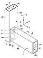
まず、図1ないし図3は本発明の参考例を示している。図において、1は参考例による導波管コーナを示している。導波管コーナ1は、後述する2本の矩形導波管2,4によって構成され、これらの矩形導波管2,4が屈曲した状態で接続されるものである。
First, FIGS. 1 to 3 show a reference example of the present invention . In the figure,
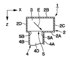
2は例えば管軸がY軸方向に向けて延びた中空な導体の方形管からなる第1の矩形導波管(H面導波管)を示している。矩形導波管2は、管軸に直交する長い縦寸法(X軸方向寸法)を有して互いに対向した一対のH面管壁2A,2Bと、管軸に直交する短い横寸法(Z軸方向寸法)を有し該H面管壁2A,2Bの両端側に位置して一対のH面管壁2A,2B間を接続するE面管壁2C,2Dとによって断面矩形状に形成されている。ここで、H面管壁2A,2Bは、内部の磁界と平行な方向としてX軸方向に延びて矩形断面の長辺を形成している。一方、E面管壁2C,2Dは、内部の電界と平行な方向としてZ軸方向に延びて矩形断面の短辺を形成している。また、矩形導波管2のY軸方向の終端側は導体板からなる終端管壁3によって閉塞されている。そして、矩形導波管2内には、Z軸に平行な電界E(電界ベクトル)が形成され、例えばTE10モードの電磁波(例えばマイクロ波、ミリ波等の高周波信号)が管軸(Y軸方向)に沿って伝搬する。このとき、H面管壁2A,2BのうちX軸方向(幅方向)の中心に位置する中心軸O1付近で2つの矩形導波管2,4が重なる領域において、後述する開口5の辺5Aに垂直になるように電界Eが入射している。
4は管軸がZ軸方向に向けて延びた中空な導体の方形管からなる第2の矩形導波管(E面導波管)を示している。第2の矩形導波管4は、第1の矩形導波管2とほぼ同様に、管軸に直交する長い縦寸法(Y軸方向寸法)を有して互いに対向した一対のH面管壁4A,4Bと、管軸に直交する短い横寸法(X軸方向寸法)を有し該H面管壁4A,4Bの両端側に位置して一対のH面管壁4A,4B間を接続するE面管壁4C,4Dとによって断面矩形状に形成されている。
また、矩形導波管4のZ軸方向の端面は、矩形導波管2のH面管壁2Aに開口している。このとき、矩形導波管2のH面管壁2Aには、矩形導波管4の断面形状とほぼ同じ形状の矩形の開口5が形成されている。そして、開口5は、管壁4A〜4Dに沿った4辺5A〜5Dを有すると共に、2本の矩形導波管2,4は、該開口5を通じてそれぞれの内部が連通している。
Further, the end surface in the Z-axis direction of the
また、第2の矩形導波管4のH面管壁4A,4Bは、内部の磁界と平行な方向として第1の矩形導波管2の管軸をなすY軸方向に平行に延び、矩形断面の長辺を形成している。一方、E面管壁4C,4Dは、内部の電界と平行な方向としてX軸方向に延びて矩形断面の短辺を形成している。ここで、第2の矩形導波管4のE面管壁4C,4Dは、当該E面管壁4C,4DのX軸方向の中心に位置する中心軸O2が第1の矩形導波管2のH面管壁2Aの中心軸O1に対して位置ずれした状態で配置されている。これにより、第2の矩形導波管4の一方のH面管壁4Aは、第1の矩形導波管2のH面管壁2Aの中心軸O1近傍に位置し、他方のH面管壁4Bは、第1の矩形導波管2のH面管壁2Aの中心軸O1から離れてE面管壁2D近傍に位置している。
The H-
そして、矩形導波管4内には、X軸に平行な電界E(電界ベクトル)が形成され、例えばTE10モードと直交する偏波面を有するTE01モードの電磁波が管軸(Z軸方向)に沿って伝搬する。このとき、2つの矩形導波管2,4が重なる領域(矩形導波管4が矩形導波管2に開口した領域)において、図3に示すように、H面管壁2Aの中心軸O1近傍に位置して中心軸O1に沿った辺5Aに対して、垂直になるように電界Eが入射している。
An electric field E (electric field vector) parallel to the X axis is formed in the
参考例による導波管コーナ1は上述の如き構成を有するもので、次にその作動について説明する。
The
まず、第1の矩形導波管2に対してZ軸方向に平行な電界EをもったTE10モードの電磁波(マイクロ波等)を入力すると、該電磁波は、矩形導波管2内を伝搬して開口5が設けられた終端側に到達する。そして、矩形導波管2の終端側に到達した電磁波は、その一部が開口5を通じて第2の矩形導波管4内に進入し、矩形導波管4に沿ってZ軸方向に伝搬する。
First, when a TE10 mode electromagnetic wave (such as a microwave) having an electric field E parallel to the Z-axis direction is input to the first
然るに、参考例によれば、第1の矩形導波管2のH面管壁2Aには第2の矩形導波管4の端面を開口させるから、第1の矩形導波管2のH面管壁2Aに対して例えば垂直な方向に向けて第2の矩形導波管4を接続することができる。また、第2の矩形導波管4のH面管壁4A,4BとE面管壁4C,4Dとは、その管軸(Z軸方向)に対してそれぞれ直交したY軸方向とX軸方向とに延びる構成となっている。これに対して、第2の矩形導波管4のH面管壁4A,4Bは第1の矩形導波管2の管軸(Y軸方向)に沿って延びる構成としたから、第2の矩形導波管4のH面管壁4A,4Bを、第1の矩形導波管2のH面管壁2Aに対して垂直な方向に延伸させることができる。
However, according to the reference example , since the end surface of the second
このため、第1の矩形導波管2の偏波面と第2の矩形導波管4の偏波面とを互いに直交させることができるから、導波管コーナ1に偏波面の変換作用をもたせることができる。また、2本の矩形導波管2,4のH面管壁2A,4Aはそれぞれ異なる平面を形成するから、第1の矩形導波管2のH面管壁2Aに対して例えば垂直な方向に向けて第2の矩形導波管4を伸長させることができる。この結果、偏波面の変換作用と矩形導波管2,4の屈曲方向との組み合わせとして、従来技術によるHコーナ、Eコーナには存在しない組み合わせを実現することができ、導波管回路のレイアウト自由度を高めて、導波管回路を小型化することができる。
For this reason, since the polarization plane of the first
特に、参考例では、第2の矩形導波管4のE面管壁4C,4Dの中心軸O2を第1の矩形導波管2のH面管壁2Aの中心軸O1に対して位置ずれした状態で配置している。このとき、第2の矩形導波管4の端面は第1の矩形導波管2のH面管壁2Aに開口する。このため、第2の矩形導波管4をなす2つのH面管壁4A,4Bのうち一側のH面管壁4Aを第1の矩形導波管2のH面管壁2Aの中心軸O1に近い位置に配置し、他側の(残余の)H面管壁4Bを第1の矩形導波管2のH面管壁2Aの中心軸O1から離れたE面管壁2D近傍に配置することができる。
In particular, in the reference example , the center axis O2 of the
このとき、2つの矩形導波管2,4が重なる領域においては、矩形導波管4の開口5をなす4辺5A〜5Dのうち矩形導波管2のH面管壁2Aの中心軸O1に近い辺5Aに対して、垂直になるように電界Eが入射している。この電界Eの方向は、互いの矩形導波管2,4を伝搬するモードの電界Eを合成する方向であり、これにより偏波面の変換が可能となる。この結果、第1,第2の矩形導波管2,4の間で偏波面の変換を行うことができ、互いの電界成分を直交させることができる。
At this time, in the region where the two
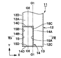
次に、図4ないし図7は本発明の第1の実施の形態を示している。そして、本実施の形態の特徴は、第2の矩形導波管のH面管壁が、第1の矩形導波管のE面管壁に対して同一平面を形成する構成としたことにある。 4 to 7 show a first embodiment of the present invention. The feature of the present embodiment is that the H-plane tube wall of the second rectangular waveguide forms a same plane with respect to the E-plane tube wall of the first rectangular waveguide. .
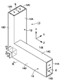
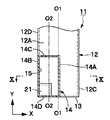
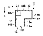
11は第1の実施の形態による導波管コーナを示している。導波管コーナ11は、後述する2本の矩形導波管12,14によって構成され、これらの矩形導波管12,14が屈曲した状態で接続されるものである。
12は例えば管軸がY軸方向に向けて延びた中空な導体の方形管からなる第1の矩形導波管(H面導波管)を示している。矩形導波管12は、参考例による矩形導波管2とほぼ同様に、管軸に直交する長い縦寸法(X軸方向寸法)を有して互いに対向した一対のH面管壁12A,12Bと、管軸に直交する短い横寸法(Z軸方向寸法)を有し該H面管壁12A,12Bの両端側に位置して一対のH面管壁12A,12B間を接続するE面管壁12C,12Dとによって断面矩形状に形成されている。
ここで、H面管壁12A,12Bは、内部の磁界と平行な方向としてX軸方向に延びて矩形断面の長辺を形成している。一方、E面管壁12C,12Dは、内部の電界と平行な方向としてZ軸方向に延びて矩形断面の短辺を形成している。また、矩形導波管12のY軸方向の終端側は導体板からなる終端管壁13によって閉塞されている。そして、矩形導波管12内には、Z軸に平行な電界E(電界ベクトル)が形成され、例えばTE10モードの電磁波が管軸(Y軸方向)に沿って伝搬する。
Here, the H-
14は管軸がZ軸方向に向けて延びた中空な導体の方形管からなる第2の矩形導波管(E面導波管)を示している。第2の矩形導波管14は、参考例による矩形導波管4とほぼ同様に、管軸に直交する長い縦寸法(Y軸方向寸法)を有して互いに対向した一対のH面管壁14A,14Bと、管軸に直交する短い横寸法(X軸方向寸法)を有し該H面管壁14A,14Bの両端側に位置して一対のH面管壁14A,14B間を接続するE面管壁14C,14Dとによって断面矩形状に形成されている。
また、矩形導波管14のZ軸方向の端面は、矩形導波管12のH面管壁12Aに開口している。このとき、矩形導波管12のH面管壁12Aの角隅には、矩形導波管14の断面形状とほぼ同じ形状の矩形の開口15が形成されている。そして、開口15は、管壁14A〜14Dに沿った4辺15A〜15Dを有すると共に、2本の矩形導波管12,14は、該開口15を通じてそれぞれの内部が連通している。
Further, the end surface in the Z-axis direction of the
また、第2の矩形導波管14のH面管壁14A,14Bは、内部の磁界と平行な方向として第1の矩形導波管12の管軸をなすY軸方向に沿って延び、矩形断面の長辺を形成している。一方、E面管壁14C,14Dは、内部の電界と平行な方向としてX軸方向に延びて矩形断面の短辺を形成している。
The H-
ここで、第2の矩形導波管14のE面管壁14C,14Dは、当該E面管壁14C,14DのX軸方向の中心に位置する中心軸O2が第1の矩形導波管12のH面管壁12Aの中心軸O1に対して位置ずれした状態で配置されている。また、第2の矩形導波管14の2つのH面管壁14A,14Bのうち一方のH面管壁14Aは、第1の矩形導波管12のH面管壁12Aの中心軸O1付近に位置し、他方のH面管壁14Bは、第1の矩形導波管12の2つのE面管壁12C,12Dのうち一方のE面管壁12Dに連続して同一平面を形成している。
Here, the
そして、矩形導波管14内には、X軸に平行な電界E(電界ベクトル)が形成され、例えばTE10モードと直交する偏波面を有するTE01モードの電磁波が管軸(Z軸方向)に沿って伝搬するものである。
An electric field E (electric field vector) parallel to the X axis is formed in the
かくして、本実施の形態でも参考例と同様の作用効果を得ることができる。特に、本実施の形態では、第2の矩形導波管14のH面管壁14Bは第1の矩形導波管12のE面管壁12Dに対して同一平面を形成する構成とした。このため、第2の矩形導波管14のH面管壁14Bと第1の矩形導波管12のE面管壁12Dとを一緒に形成することができる。この結果、導波管コーナ11を、例えば金属の切削加工、射出成形、プレス加工等のような種々の成形工法を用いて成形、加工することができ、成形性、生産性、量産性を高めることができる。
Thus, the same effects as in the reference example can be obtained in this embodiment. In particular, in the present embodiment, the H-
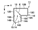
また、第2の矩形導波管14のH面管壁14Bは第1の矩形導波管12のE面管壁12Dに対して同一平面を形成する構成としたから、第2の矩形導波管14のH面管壁14Bを第1の矩形導波管12のE面管壁12Dに連続させることができ、残余のH面管壁12Aを矩形導波管12のH面管壁12Aの中心軸O1付近に配置することができる。このとき、2つの矩形導波管12,14が重なる領域(矩形導波管14が矩形導波管12に開口した領域)においては、図6に示すように、矩形導波管14の開口15をなす4辺15A〜15Dのうち矩形導波管12のH面管壁12Aの中心軸O1に近い辺15A(エッジ部分)に対して、垂直になるように電界Eは入射している。この電界Eの方向は、互いの矩形導波管12,14を伝搬するモードの電界Eを合成する方向であり、これにより偏波面の変換が可能となる。この結果、第1の矩形導波管12と第2の矩形導波管14との間で偏波面の変換を行い、電界成分を直交させることができる。
Further, since the H-
特に、一般的な矩形導波管(例えばWR−10等)では、矩形開口のうち長辺側(H面管壁側)の縦寸法Aが短辺側(E面管壁側)の横寸法Bに対して2倍の値(A=2×B)となっている。本実施の形態による矩形導波管12,14に対して、このような一般的な矩形導波管を適用した場合には、第2の矩形導波管14の2つのH面管壁14A,14BのうちH面管壁14Bが第1の矩形導波管12のE面管壁12Dに連続して同一平面を形成するから、残余のH面管壁14Aは第1の矩形導波管12のH面管壁12Aのうち中心軸O1上に配置されることになる。このとき、第1の矩形導波管12内にはTE10モードの電磁波が伝搬するから、エッジ部分(辺15A部分)では電界ベクトルがエッジ部分に直交するように入射される。このため、エッジ部分の周囲では互いに接続したH面管壁14BとE面管壁12Dとの電界ベクトルを合成したベクトル方向となるから、第1,第2の矩形導波管12,14間でモードの変換が可能となると共に、反射損失が低減される。
In particular, in a general rectangular waveguide (for example, WR-10), the vertical dimension A on the long side (H plane tube wall side) of the rectangular opening is the horizontal dimension on the short side (E plane tube wall side). The value is twice that of B (A = 2 × B). When such a general rectangular waveguide is applied to the
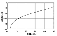
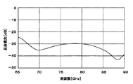
ここで、導波管コーナ11の反射損失を検討した。第1,第2の矩形導波管12,14としては標準的な矩形導波管WR−10を用いた場合を想定し、この場合の反射損失を電磁界シミュレーション等を用いて算出した。この結果を図7に示す。なお、第1,第2の矩形導波管12,14の矩形開口のうち長辺側の縦寸法Aは2.54mm、短辺側の横寸法Bは1.27mmとしている。図7の結果より、73GHz以下の周波数帯域では反射損失が−15dBよりも低減でき、第1,第2の矩形導波管12,14間で損失を低減しつつ、モード変換を伴った電磁波の伝送が可能となることが確認できた。
Here, the reflection loss of the
次に、図8ないし図11は本発明の第2の実施の形態を示している。そして、本実施の形態の特徴は、第1の矩形導波管には第2の矩形導波管の開口端面の近傍に位置して2つの矩形導波管のモードを整合させるための整合用導波素子を設けたことにある。なお、本実施の形態では、第1の実施の形態と同一の構成要素に同一の符号を付し、その説明を省略するものとする。 Next, FIGS. 8 to 11 show a second embodiment of the present invention. The feature of the present embodiment is that the first rectangular waveguide is positioned near the opening end face of the second rectangular waveguide and is used for matching the modes of the two rectangular waveguides. A waveguide element is provided. In the present embodiment, the same reference numerals in the first same components as in the embodiment, a description thereof is omitted.
21は第1の矩形導波管12の終端側に設けられた整合用導波素子としての導体凸部を示している。導体凸部21は、例えば管壁12A〜12Dと同様な導体材料(導電性材料)によって形成され、第2の矩形導波管14の開口端面をなす開口15の近傍として、E面管壁12D、終端管壁13、H面管壁12Bが交わる角隅に設けられている。そして、導体凸部21は、略直方体形状をなして矩形導波管12の内部に突出している。これにより、導体凸部21の突出端側に電界が集中するから、第1,第2の矩形導波管12,14間でモード変換が容易となり、整合帯域を広帯域化することができる。
ここで、導体凸部21による効果を検討した。第1,第2の矩形導波管12,14としては標準的な矩形導波管WR−10を用いた場合を想定し、この場合の反射損失を電磁界シミュレーション等を用いて算出した。この結果を図11に示す。なお、第1,第2の矩形導波管12,14の矩形開口のうち長辺側の縦寸法Aは2.54mm、短辺側の横寸法Bは1.27mmとしている。また、導体凸部21のX軸方向寸法C1、Y軸方向寸法C2、Z軸方向寸法C3は、0.80mm(C1=0.80mm)、0.80mm(C2=0.80mm)、0.90mm(C3=0.90mm)としている。図11の結果より、65GHzから90GHzの周波数帯域では反射損失が−15dBよりも低減でき、導体凸部21を設けない場合(図7参照)に比べて整合帯域が広帯域化できることが分かった。
Here, the effect by the conductor
かくして、本実施の形態でも第1の実施の形態および参考例と同様の作用効果を得ることができる。特に、本実施の形態では、第1の矩形導波管12内には第2の矩形導波管14の開口端面(開口15)の近傍に位置して導体凸部21を設けた。このため、例えば導体凸部21の先端側に電界を集中させて第1の矩形導波管12内を伝搬するTE10モードと第2の矩形導波管14内を伝搬するTE10モードとの間の整合性を高めることができる。これにより、2本の矩形導波管12,14間での反射損失を低減することができ、整合帯域を広帯域化することができる。
Thus, this embodiment can provide the same effects as those of the first embodiment and the reference example . In particular, in the present embodiment, the conductor
また、整合用導波素子を第1の矩形導波管12の内部に突出した導体凸部21によって構成したから、第1の矩形導波管12の管壁12A〜12D等を加工するときに一緒に導体凸部21を形成することができ、加工性、量産性を高めることができる。
In addition, since the matching waveguide element is constituted by the conductor
なお、前記第2の実施の形態では、整合用導波素子として導体凸部21を用いるものとした。しかし、本発明はこれに限らず、例えば整合用導波素子として第1の矩形導波管12内に突出した金属製のボルト等を用いてもよい。この場合、ボルトの突出寸法を適宜変化させることによって、整合性等の調整が可能となる。
In the second embodiment, the conductor
次に、図12は本発明の第3の実施の形態を示している。そして、本実施の形態の特徴は、導波管コーナを用いて無線装置としてのレーダ装置を構成したことにある。なお、本実施の形態では、第1の実施の形態と同一の構成要素に同一の符号を付し、その説明を省略するものとする。 Next, FIG. 12 shows a third embodiment of the present invention. The feature of this embodiment is that a radar device as a wireless device is configured using a waveguide corner. In the present embodiment, the same components as those in the first embodiment are denoted by the same reference numerals, and the description thereof is omitted.
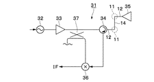
31は本実施の形態による無線装置としてのレーダ装置を示している。レーダ装置31は、電圧制御発振器32と、該電圧制御発振器32に増幅器33、サーキュレータ34を介して接続されたアンテナ35(放射器)と、該アンテナ35から受信した信号を中間周波信号IFにダウンコンバートするためにサーキュレータ34に接続されたミキサ36とによって概略構成されている。また、増幅器33とサーキュレータ34との間には方向性結合器37が接続して設けられている。そして、この方向性結合器37によって電力分配された信号は、ミキサ36にローカル信号として入力される。また、サーキュレータ34とアンテナ35との間は、矩形導波管12,14を用いて接続されると共に、矩形導波管12,14の屈曲部分には導波管コーナ11が設けられている。
本実施の形態によるレーダ装置31は、上述の如き構成を有している。電圧制御発振器32から出力された発振信号は、増幅器33によって増幅され、方向性結合器37およびサーキュレータ34を経由して、送信信号としてアンテナ35から送信(放射)される。一方、アンテナ35から受信された受信信号は、サーキュレータ34を通じてミキサ36に入力されると共に、方向性結合器37によるローカル信号を用いてダウンコンバートされ、中間周波信号IFとして出力される。
The
かくして、本実施の形態によれば、導波管コーナ11を用いてレーダ装置31を構成したから、アンテナ35の接続部分等に偏波面の変換(モード変換)が可能な導波管コーナ11を適用してレーダ装置31のレイアウト自由度を高めることができると共に、装置全体を小型化することができる。
Thus, according to this embodiment, since the configuration of the
なお、前記第3の実施の形態では、本発明による導波管コーナ11をレーダ装置31に適用した場合を例を挙げて説明したが、例えば無線装置としての通信装置等に適用してもよい。
In the third embodiment, the case where the
また、前記第3の実施の形態では、第1の実施の形態による導波管コーナ11を用いるものとしたが、第2の実施の形態による導波管コーナ11を用いる構成としてもよい。
In the third embodiment, the
また、前記各実施の形態では、導波管として断面矩形状の矩形導波管12,14を用いる構成とした。しかし、本発明はこれに限らず、例えば図13に示す変形例のように、第1管壁41A,41B(H面管壁)と第2管壁41C,41D(E面管壁)とからなり、角隅にC面、R面等の面取り部41Eを形成された断面略矩形状の矩形導波管41を用いる構成としてもよい。 Also, in each embodiment, and the configuration using the rectangular cross section of the
また、前記各実施の形態では、矩形導波管12,14内は中空に形成するものとしたが、例えば内部に誘電体が装荷(挿入)された導波管を用いる構成としてもよい。
Also, in each embodiment, although the
また、前記各実施の形態では、第2の矩形導波管14は第1の矩形導波管12のH面管壁12Aに対して垂直方向に延びる構成としたが、垂直方向に限らず垂直方向から斜めに傾斜した方向に延びる構成としてもよい。
Further, in each embodiment, the second
1,11 導波管コーナ
2,4,12,14,41 矩形導波管
2A,2B,4A,4B,12A,12B,14A,14B H面管壁
2C,2D,4C,4D,12C,12D,14C,14D E面管壁
3,13 終端管壁
5,15 開口
21 導体凸部(整合用導波素子)
31 レーダ装置
41A,41B 第1管壁(H面管壁)
41C,41D 第2管壁(E面管壁)
1,11
31 radar equipment
4 1A, 41 B 1st pipe wall (H face pipe wall )
41C, 41 D second wall (E Menkankabe)
Claims (4)
前記2本の導波管は、管軸に直交する長い縦寸法を有し互いに対向すると共に、磁界と平行な一対のH面管壁と、管軸に直交する短い横寸法を有し該H面管壁の両端側に位置して一対のH面管壁間を接続すると共に、電界と平行な一対のE面管壁と、からなる断面矩形状の矩形導波管によってそれぞれ構成し、
前記2本の導波管のうち一方の矩形導波管のH面管壁には、前記2本の導波管のうち他方の矩形導波管の端面を開口させると共に、該他方の矩形導波管のH面管壁が前記一方の矩形導波管の管軸に平行である構成とし、
前記他方の矩形導波管のH面管壁は、前記一方の矩形導波管のE面管壁に対して同一平面を形成する構成としたことを特徴とする導波管コーナ。In a waveguide corner that connects two waveguides in a bent state,
The two of the waveguide is adapted to face each other has a longer longitudinal dimension perpendicular to the tube axis, said has a pair of H surfaces wall parallel to the magnetic field, the short transverse dimension perpendicular to the tube axis H located at opposite ends of the face wall with connecting a pair of H-plane tube walls, constitute respectively the electric field parallel to a pair of E surfaces tube wall, the rectangular cross section of the rectangular waveguide Ru Tona,
Wherein the H-plane wall of the rectangular waveguide of one of the two waveguides, causes opening the end face of the other of the rectangular waveguide of the two waveguides, a rectangular guide of said other a configuration H surface wall of the wave tube is parallel to the tube axis of the rectangular waveguide of the one,
H Menkankabe of the other rectangular waveguide is a waveguide corner, characterized in that it has a configuration that form a flush against E plane tube wall of the rectangular waveguide of the one.
Applications Claiming Priority (3)
| Application Number | Priority Date | Filing Date | Title |
|---|---|---|---|
| JP2004100046 | 2004-03-30 | ||
| JP2004100046 | 2004-03-30 | ||
| PCT/JP2005/004059 WO2005099026A1 (en) | 2004-03-30 | 2005-03-09 | Waveguide corner and radio device |
Publications (2)
| Publication Number | Publication Date |
|---|---|
| JPWO2005099026A1 JPWO2005099026A1 (en) | 2008-03-06 |
| JP4111237B2 true JP4111237B2 (en) | 2008-07-02 |
Family
ID=35125397
Family Applications (1)
| Application Number | Title | Priority Date | Filing Date |
|---|---|---|---|
| JP2006511926A Expired - Fee Related JP4111237B2 (en) | 2004-03-30 | 2005-03-09 | Waveguide corner and radio equipment |
Country Status (3)
| Country | Link |
|---|---|
| US (1) | US7750762B2 (en) |
| JP (1) | JP4111237B2 (en) |
| WO (1) | WO2005099026A1 (en) |
Cited By (1)
| Publication number | Priority date | Publication date | Assignee | Title |
|---|---|---|---|---|
| US8218406B2 (en) | 2008-05-21 | 2012-07-10 | Nidec Copal Corporation | Lens driving apparatus |
Families Citing this family (19)
| Publication number | Priority date | Publication date | Assignee | Title |
|---|---|---|---|---|
| JP4862530B2 (en) * | 2006-07-25 | 2012-01-25 | 日本電気株式会社 | Waveguide |
| GB0807196D0 (en) * | 2008-04-19 | 2008-05-28 | Raven Mfg Ltd | Data receiving apparatus |
| KR101092954B1 (en) * | 2009-12-11 | 2011-12-12 | 국방과학연구소 | Vertically Coupled Polarization Converter for Waveguides and Its Design Method |
| JP5300901B2 (en) * | 2011-03-18 | 2013-09-25 | 株式会社東芝 | Waveguide connection structure, antenna device, and radar device |
| US9041595B2 (en) * | 2011-12-19 | 2015-05-26 | Trimble Navigation Limited | Determining the location of a load for a tower crane |
| JP5780995B2 (en) * | 2012-03-27 | 2015-09-16 | 三菱電機株式会社 | Rectangular waveguide connection structure |
| JP5694246B2 (en) | 2012-07-13 | 2015-04-01 | 株式会社東芝 | Waveguide connection structure, antenna device, and radar device |
| US9105952B2 (en) | 2012-10-17 | 2015-08-11 | Honeywell International Inc. | Waveguide-configuration adapters |
| WO2015013927A1 (en) * | 2013-07-31 | 2015-02-05 | 华为技术有限公司 | Antenna |
| EP3193404A4 (en) | 2014-09-09 | 2018-04-18 | Mitsubishi Electric Corporation | Waveguide device |
| CN104201439A (en) * | 2014-09-09 | 2014-12-10 | 江苏贝孚德通讯科技股份有限公司 | Microwave waveguide pipeline 90-degree turning mechanism having polarization reverse function |
| US9711831B2 (en) * | 2015-05-08 | 2017-07-18 | Elwha Llc | Holographic mode conversion for transmission lines |
| CN105428757B (en) * | 2015-12-23 | 2019-05-21 | 江苏贝孚德通讯科技股份有限公司 | A kind of ridge waveguide turning structure of band filtering and twist-reflector function |
| CN106169633A (en) * | 2016-08-30 | 2016-11-30 | 江苏贝孚德通讯科技股份有限公司 | A kind of waveguide 90 degree turning structure |
| US10600402B2 (en) | 2017-05-18 | 2020-03-24 | Elwha Llc | Systems and methods for acoustic mode conversion |
| RU182129U1 (en) * | 2018-04-23 | 2018-08-03 | Акционерное общество "Научно-исследовательский институт Приборостроения имени В.В. Тихомирова" | DEVICE FOR ROTATING THE POLARIZATION PLANE |
| JP7402035B2 (en) * | 2019-12-18 | 2023-12-20 | Jrcモビリティ株式会社 | waveguide converter |
| CN114583429B (en) * | 2020-11-30 | 2024-04-16 | 京东方科技集团股份有限公司 | Waveguide conversion structure, waveguide feeding network and antenna system |
| DE102023200992A1 (en) * | 2023-02-08 | 2024-08-08 | Robert Bosch Gesellschaft mit beschränkter Haftung | Radiating element, waveguide antenna and method for producing a radiating element |
Family Cites Families (15)
| Publication number | Priority date | Publication date | Assignee | Title |
|---|---|---|---|---|
| US2860309A (en) * | 1953-11-17 | 1958-11-11 | Gen Precision Lab Inc | Broadband waveguide junction |
| US2854637A (en) * | 1954-01-29 | 1958-09-30 | Gen Precision Lab Inc | Matching device for magic tee |
| FR2057237A5 (en) * | 1969-08-07 | 1971-05-21 | Thomson Csf | |
| JPS55104803U (en) * | 1979-01-18 | 1980-07-22 | ||
| JPS55104803A (en) | 1979-02-02 | 1980-08-11 | Kato Kensaku | Rotary weeding plate |
| DE3824150A1 (en) * | 1988-07-16 | 1989-07-06 | Kathrein Werke Kg | SEMICONDUCTOR TWIST |
| JPH04257101A (en) | 1991-02-08 | 1992-09-11 | Nec Corp | Cross polarization demultiplexing device |
| JPH0548309A (en) | 1991-08-09 | 1993-02-26 | Matsushita Electric Works Ltd | Waveguide branch circuit |
| JPH0685502A (en) | 1992-08-31 | 1994-03-25 | Nec Corp | Orthogonal polarizer |
| JPH0746011A (en) | 1993-07-29 | 1995-02-14 | Nec Corp | Power distributor |
| JPH09246801A (en) | 1996-03-14 | 1997-09-19 | Nec Corp | Waveguide bent |
| JPH1051208A (en) | 1996-07-30 | 1998-02-20 | Nec Corp | Branching filter |
| US6563398B1 (en) * | 1999-12-23 | 2003-05-13 | Litva Antenna Enterprises Inc. | Low profile waveguide network for antenna array |
| EP1176662A1 (en) * | 2000-06-30 | 2002-01-30 | Alcatel | Waveguide polarisation rotator |
| DE10032172A1 (en) | 2000-07-01 | 2002-01-17 | Marconi Comm Gmbh | Transition for orthogonally oriented waveguides |
-
2005
- 2005-03-09 JP JP2006511926A patent/JP4111237B2/en not_active Expired - Fee Related
- 2005-03-09 US US10/586,480 patent/US7750762B2/en not_active Expired - Fee Related
- 2005-03-09 WO PCT/JP2005/004059 patent/WO2005099026A1/en not_active Ceased
Cited By (1)
| Publication number | Priority date | Publication date | Assignee | Title |
|---|---|---|---|---|
| US8218406B2 (en) | 2008-05-21 | 2012-07-10 | Nidec Copal Corporation | Lens driving apparatus |
Also Published As
| Publication number | Publication date |
|---|---|
| JPWO2005099026A1 (en) | 2008-03-06 |
| WO2005099026A1 (en) | 2005-10-20 |
| US20080238579A1 (en) | 2008-10-02 |
| US7750762B2 (en) | 2010-07-06 |
Similar Documents
| Publication | Publication Date | Title |
|---|---|---|
| JP4111237B2 (en) | Waveguide corner and radio equipment | |
| JP4884532B2 (en) | Transmission line converter | |
| US20100225410A1 (en) | Waveguide to microstrip transition | |
| US7002429B2 (en) | Nonreflective waveguide terminator and waveguide circuit | |
| CN110692164B (en) | Nonreciprocal Mode Conversion Substrate Integrated Waveguide | |
| WO2018116416A1 (en) | Waveguide-microstrip line converter and antenna device | |
| CN109478705B (en) | Coaxial to Waveguide Converter | |
| CN114188686B (en) | H-face waveguide/microstrip probe conversion device | |
| JP2011223203A (en) | Waveguide/planar line converter and high frequency circuit | |
| JP6219324B2 (en) | Planar transmission line waveguide converter | |
| KR100852377B1 (en) | Nrd guide mode suppressor | |
| JP3485054B2 (en) | Different type non-radiative dielectric line converter structure and device | |
| JP3013798B2 (en) | Crossing track | |
| JP3820234B2 (en) | High frequency module | |
| JP2003174305A (en) | Transmission line and transmitter-receiver | |
| US20210203051A1 (en) | Microwave circulator based on dielectric waveguides | |
| JP5053245B2 (en) | 180 degree hybrid | |
| JP3846585B2 (en) | Waveguide bend, waveguide plate and high frequency device | |
| JP3259637B2 (en) | Transceiver | |
| JP4224909B2 (en) | Line conversion structure, high-frequency circuit, and wireless device | |
| JP2003163502A (en) | Transmission line and transmitter-receiver | |
| JP2008079085A (en) | Transmission line waveguide converter | |
| JP7113986B2 (en) | Converter and antenna device | |
| JP4103330B2 (en) | NRD guide L type antenna element | |
| JP2002217613A (en) | Transmission line, integrated circuit and transmitting/ receiving device |
Legal Events
| Date | Code | Title | Description |
|---|---|---|---|
| A131 | Notification of reasons for refusal |
Free format text: JAPANESE INTERMEDIATE CODE: A131 Effective date: 20071218 |
|
| A521 | Request for written amendment filed |
Free format text: JAPANESE INTERMEDIATE CODE: A523 Effective date: 20080214 |
|
| TRDD | Decision of grant or rejection written | ||
| A01 | Written decision to grant a patent or to grant a registration (utility model) |
Free format text: JAPANESE INTERMEDIATE CODE: A01 Effective date: 20080318 |
|
| A61 | First payment of annual fees (during grant procedure) |
Free format text: JAPANESE INTERMEDIATE CODE: A61 Effective date: 20080331 |
|
| R150 | Certificate of patent or registration of utility model |
Free format text: JAPANESE INTERMEDIATE CODE: R150 |
|
| FPAY | Renewal fee payment (event date is renewal date of database) |
Free format text: PAYMENT UNTIL: 20110418 Year of fee payment: 3 |
|
| FPAY | Renewal fee payment (event date is renewal date of database) |
Free format text: PAYMENT UNTIL: 20110418 Year of fee payment: 3 |
|
| FPAY | Renewal fee payment (event date is renewal date of database) |
Free format text: PAYMENT UNTIL: 20120418 Year of fee payment: 4 |
|
| FPAY | Renewal fee payment (event date is renewal date of database) |
Free format text: PAYMENT UNTIL: 20130418 Year of fee payment: 5 |
|
| FPAY | Renewal fee payment (event date is renewal date of database) |
Free format text: PAYMENT UNTIL: 20140418 Year of fee payment: 6 |
|
| LAPS | Cancellation because of no payment of annual fees |