JP4107654B2 - High frequency switch - Google Patents
High frequency switch Download PDFInfo
- Publication number
- JP4107654B2 JP4107654B2 JP2003076175A JP2003076175A JP4107654B2 JP 4107654 B2 JP4107654 B2 JP 4107654B2 JP 2003076175 A JP2003076175 A JP 2003076175A JP 2003076175 A JP2003076175 A JP 2003076175A JP 4107654 B2 JP4107654 B2 JP 4107654B2
- Authority
- JP
- Japan
- Prior art keywords
- diode
- diodes
- input
- output
- switch
- Prior art date
- Legal status (The legal status is an assumption and is not a legal conclusion. Google has not performed a legal analysis and makes no representation as to the accuracy of the status listed.)
- Expired - Fee Related
Links
Images
Classifications
-
- H—ELECTRICITY
- H03—ELECTRONIC CIRCUITRY
- H03K—PULSE TECHNIQUE
- H03K17/00—Electronic switching or gating, i.e. not by contact-making and –breaking
- H03K17/51—Electronic switching or gating, i.e. not by contact-making and –breaking characterised by the components used
- H03K17/74—Electronic switching or gating, i.e. not by contact-making and –breaking characterised by the components used by the use, as active elements, of diodes
- H03K17/76—Switching arrangements with several input- or output-terminals, e.g. multiplexers, distributors
-
- H—ELECTRICITY
- H01—ELECTRIC ELEMENTS
- H01P—WAVEGUIDES; RESONATORS, LINES, OR OTHER DEVICES OF THE WAVEGUIDE TYPE
- H01P1/00—Auxiliary devices
- H01P1/10—Auxiliary devices for switching or interrupting
- H01P1/15—Auxiliary devices for switching or interrupting by semiconductor devices
Description
【0001】
【発明の属する技術分野】
本発明は、無線機器などに使用される高周波スイッチに関する。
【0002】
【従来の技術】
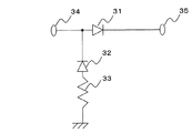
図3に、例えばアンテナを送受共用とした無線機器の受信側などに使用される従来のマイクロ波スイッチの例として、ダイオードを用いた1入力1出力スイッチ(以下、SPSTスイッチと呼ぶ)を示す。
【0003】
図3において、ダイオード31をオン状態とし、ダイオード32をオフ状態とすると、入力端子34より入力された高周波信号は出力端子35に出力される。この状態を通過状態と呼ぶことにする。
【0004】
一方、ダイオード31をオフ状態とし、ダイオード32をオン状態とすると入力端子34より入力された高周波信号は、ダイオード32を通過し終端抵抗33に吸収される。この状態を吸収状態と呼ぶことにする。
【0005】
図3に示すこのSPSTスイッチでは、吸収状態において、入力端子34のVSWRは、入力信号が終端抵抗33に吸収されているため、十分良好なものとなっている。しかしながら、出力端子35のVSWRは、ダイオード31がオフ状態となっているため、ほぼ全反射に近く、VSWRも劣化するという問題があった。
【0006】
また、従来の高周波スイッチの他の例として、FETを用いた1入力多出力スイッチが、特許文献1に記載されている。この高周波スイッチにおいては、あるFETがオン状態となって入力信号が出力端子に出力されるときに、オフ状態となっている他のFETのオフ時容量による導通ロスを防止するためインダクタを利用している。しかし、入力端子や出力端子のVSWRの劣化を改善することについては、考慮されていない。
【0007】
【特許文献1】
特開平9−181641号公報(第2頁、図1)
【0008】
【発明が解決しようとする課題】
以上述べたように、図3に示す従来のSPSTスイッチでは、スイッチ回路の吸収状態において、入力端子側に終端抵抗を接続することにより入力側のVSWRを良好にするものの、出力側は全反射に近く、VSWRの劣化を招いていた。
【0009】
そこで、本発明は、従来のこのような点に鑑みて為されたもので、スイッチ回路のオフ状態において、良好な入出力VSWRを得ることが可能な高周波スイッチを提供することを目的とする。
【0010】
【課題を解決するための手段】
本発明に係る高周波スイッチは、一つの入力端子と複数の出力端子の各々との間の信号経路に複数の第1のダイオードの各々を接続し、第1のダイオードの入力端子側に第2のダイオードの一端を接続し、第2のダイオードの他端に第1の抵抗を接続して終端し、第1のダイオードの各々の出力端子側に複数の第3のダイオードの各々の一端を接続し、複数の第3のダイオードの各々の他端に第2の抵抗をそれぞれ接続して終端することを特徴とする。
【0011】
このような構成の本発明では、一つの入力端子と複数の出力端子の各々との間の信号経路のダイオードの入力端子側および出力端子側に、信号経路のダイオードと並列になるように、ダイオードと終端抵抗をそれぞれ設けることにより、オフ状態としたスイッチ回路の入力側、出力側とも、良好なVSWRを形成することができる。
【0013】
【発明の実施の形態】
以下、図面を参照して本発明の実施形態について詳細に説明する。
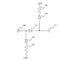
【0014】
本発明に係る高周波スイッチの一実施形態としての、マイクロ波スイッチの1つであるSPSTスイッチの構成を図1に示す。
【0015】
図1に示すように、このSPSTスイッチは、入力端子16と出力端子17との間の信号経路に、スイッチング動作を行う第1のダイオード11を接続し、第1のダイオード11の入力端子側に、第1のダイオード11と並列になるように、第2のダイオード12の一端を接続し、更に第2のダイオード12の他端に、通常50Ωで形成される終端抵抗13を接続する。次に、第1のダイオード11の出力端子側に、第1のダイオード11と並列になるように、第3のダイオード14の一端を接続し、更に第3のダイオード14の他端に通常50Ωで形成される終端抵抗15を接続する。なお、図3では記載を省略しているが、第1乃至第3のダイオード11、12、13のそれぞれをオン・オフさせるために、各ダイオード11、12、13の各端の適宜の位置にコンデンサを接続するとともに、各ダイオード11、12、13に直流バイアスを与えるための回路を接続する。
【0016】
このように構成されたSPSTスイッチにおいて、第1のダイオード11をオン状態とし、第2及び第3のダイオード12、14をオフ状態とすると、入力端子16から入力された高周波信号は出力端子17に出力される。
【0017】
一方、第1のダイオード11をオフ状態とし、第2及び第3のダイオード12、14をオン状態とすると、入力端子16から入力された高周波信号は第2のダイオード12を通過し、終端抵抗13に吸収される。このとき、入力端子16のVSWRは、終端抵抗13を、入力側の外部回路のインピーダンスとほぼ等しい50Ωに選ぶことにより、十分良好な性能を得ることができる。また、出力端子17のVSWRについても、第3のダイオード14をオン状態とし、この第3のダイオード14に50Ωの終端抵抗15を接続することにより、外部回路(インピーダンス50Ω)と整合をとることができ、良好なVSWRを得ることができる。
【0018】
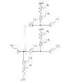
なお、上述の説明では、一実施形態として、SPSTスイッチの場合について説明したが、本発明は、これに限らず、ダイオードを用いた1入力多出力スイッチにも適用することができる。
【0019】
例えば、図2は、本発明の他の実施形態としての、1入力2出力のマイクロ波スイッチの構成を示すものである。図2においては、入力端子16と複数の出力端子171、172の各々との間の信号経路に、スイッチング動作を行う複数の第1のダイオード111、112を接続し、第1のダイオード111、112の入力端子側に、第1のダイオード111、112と並列になるように、第2のダイオード12の一端を接続し、更に第2のダイオード12の他端に、通常50Ωで形成される終端抵抗13を接続する。次に、複数の第1のダイオード111、112の各々の出力端子側に、第1のダイオード111、112の各々と並列になるように、複数の第3のダイオード141、142の各々の一端を接続し、更に第3のダイオード141、142の各々の他端に通常50Ωで形成される終端抵抗151、152をそれぞれ接続する。
【0020】
この図2に示す1入力2出力スイッチの場合も、複数の第1のダイオード111、112の少なくとも1つをオン状態にしたときは、第2のダイオード12をオフ状態とするとともに、オン状態にした第1のダイオードに対応する第3のダイオードをオフ状態とし、オフ状態にした第1のダイオードに対応する第3のダイオードをオン状態とする。また複数の第1のダイオード111、112の全てをオフ状態にしたときは、第2のダイオード12および複数の第3のダイオード141、142の全てをオン状態とする。このようにすることにより、オフ状態としたスイッチ回路の入力側、出力側とも、良好なVSWRを得ることができる。
【0021】
【発明の効果】
以上のように、本発明によれば、信号経路のダイオードの入力端子側および出力端子側に、信号経路のダイオードと並列になるように、ダイオードと終端抵抗とをそれぞれ接続することにより、スイッチ回路のオフ状態において、良好な入出力VSWRを得ることができる。
【図面の簡単な説明】
【図1】 本発明に係る高周波スイッチの一実施形態の構成図。
【図2】 本発明に係る高周波スイッチの他の実施形態の構成図。
【図3】 従来の高周波スイッチの構成図。
【符号の説明】
11、111、112…第1のダイオード
12…第2のダイオード
13、15、151、152…終端抵抗
14、141、142…第3のダイオード
16…入力端子
17、171、172…出力端子[0001]
BACKGROUND OF THE INVENTION
The present invention relates to a high-frequency switch used for a wireless device or the like.
[0002]
[Prior art]
FIG. 3 shows a one-input one-output switch (hereinafter referred to as an SPST switch) using a diode as an example of a conventional microwave switch used on the receiving side of a wireless device that uses an antenna for both transmission and reception.
[0003]
In FIG. 3, when the
[0004]
On the other hand, when the
[0005]
In the SPST switch shown in FIG. 3, in the absorption state, the VSWR of the
[0006]
As another example of a conventional high-frequency switch, Patent Document 1 discloses a one-input multi-output switch using an FET. In this high-frequency switch, when a certain FET is turned on and an input signal is output to the output terminal, an inductor is used to prevent conduction loss due to off-state capacitance of other FETs that are turned off. ing. However, no consideration is given to improving the deterioration of the VSWR of the input terminal or the output terminal.
[0007]
[Patent Document 1]
Japanese Patent Laid-Open No. 9-181641 (2nd page, FIG. 1)
[0008]
[Problems to be solved by the invention]
As described above, in the conventional SPST switch shown in FIG. 3, in the absorption state of the switch circuit, the termination resistance is connected to the input terminal side to improve the VSWR on the input side, but the output side is totally reflected. Nearby, VSWR was degraded.
[0009]
Therefore, the present invention has been made in view of such conventional points, and an object thereof is to provide a high-frequency switch capable of obtaining a good input / output VSWR when the switch circuit is in an OFF state.
[0010]
[Means for Solving the Problems]
High frequency switch according to the present invention, the signal path between the respective one of the input terminals and a plurality of output terminals connected to each of the plurality of first diodes, the second input terminal of the first diode Attach one end of the diode, a first resistor connected terminated, connect one end of each of the plurality of the third diode to the output terminal side of each of the first diode to the other end of the second diode , characterized by connecting a second resistor, respectively terminating at the other end of each of the plurality of third diodes.
[0011]
In the present invention having such a configuration, the diode is arranged in parallel with the diode of the signal path on the input terminal side and the output terminal side of the diode of the signal path between one input terminal and each of the plurality of output terminals. By providing each of the terminal resistors, a good VSWR can be formed on both the input side and the output side of the switch circuit in the off state.
[0013]
DETAILED DESCRIPTION OF THE INVENTION
Hereinafter, embodiments of the present invention will be described in detail with reference to the drawings.
[0014]
FIG. 1 shows the configuration of an SPST switch that is one of microwave switches as an embodiment of the high-frequency switch according to the present invention.
[0015]
As shown in FIG. 1, this SPST switch has a signal path between an
[0016]
In the SPST switch configured as described above, when the first diode 11 is turned on and the second and
[0017]
On the other hand, when the first diode 11 is turned off and the second and
[0018]
In the above description, the SPST switch has been described as an embodiment. However, the present invention is not limited to this and can be applied to a single-input multiple-output switch using a diode.
[0019]
For example, FIG. 2 shows a configuration of a microwave switch with one input and two outputs as another embodiment of the present invention. In FIG. 2, a plurality of first diodes 11 1 and 11 2 that perform a switching operation are connected to a signal path between the
[0020]
Also in the case of the 1-input 2-output switch shown in FIG. 2, when at least one of the plurality of first diodes 11 1 , 11 2 is turned on, the
[0021]
【The invention's effect】
As described above, according to the present invention, the switch circuit is formed by connecting the diode and the termination resistor to the input terminal side and the output terminal side of the diode of the signal path in parallel with the diode of the signal path, respectively. In the off state, a good input / output VSWR can be obtained.
[Brief description of the drawings]
FIG. 1 is a configuration diagram of an embodiment of a high-frequency switch according to the present invention.
FIG. 2 is a configuration diagram of another embodiment of the high-frequency switch according to the present invention.
FIG. 3 is a configuration diagram of a conventional high-frequency switch.
[Explanation of symbols]
11, 11 1, 11 2 ... first diode 12:
Claims (2)
Priority Applications (2)
| Application Number | Priority Date | Filing Date | Title |
|---|---|---|---|
| JP2003076175A JP4107654B2 (en) | 2003-03-19 | 2003-03-19 | High frequency switch |
| US10/785,062 US7015770B2 (en) | 2003-03-19 | 2004-02-25 | High frequency switch |
Applications Claiming Priority (1)
| Application Number | Priority Date | Filing Date | Title |
|---|---|---|---|
| JP2003076175A JP4107654B2 (en) | 2003-03-19 | 2003-03-19 | High frequency switch |
Publications (3)
| Publication Number | Publication Date |
|---|---|
| JP2004289281A JP2004289281A (en) | 2004-10-14 |
| JP2004289281A5 JP2004289281A5 (en) | 2005-10-20 |
| JP4107654B2 true JP4107654B2 (en) | 2008-06-25 |
Family
ID=32984805
Family Applications (1)
| Application Number | Title | Priority Date | Filing Date |
|---|---|---|---|
| JP2003076175A Expired - Fee Related JP4107654B2 (en) | 2003-03-19 | 2003-03-19 | High frequency switch |
Country Status (2)
| Country | Link |
|---|---|
| US (1) | US7015770B2 (en) |
| JP (1) | JP4107654B2 (en) |
Families Citing this family (1)
| Publication number | Priority date | Publication date | Assignee | Title |
|---|---|---|---|---|
| JP2006319435A (en) | 2005-05-10 | 2006-11-24 | Alps Electric Co Ltd | Switching circuit |
Family Cites Families (6)
| Publication number | Priority date | Publication date | Assignee | Title |
|---|---|---|---|---|
| US5170139A (en) * | 1991-03-28 | 1992-12-08 | Texas Instruments Incorporated | PIN diode switch |
| US5159296A (en) | 1991-03-28 | 1992-10-27 | Texas Instruments Incorporated | Four port monolithic gaas pin diode switch |
| JP2596488Y2 (en) * | 1992-10-01 | 1999-06-14 | アルプス電気株式会社 | Filter circuit |
| US5777530A (en) * | 1996-01-31 | 1998-07-07 | Matsushita Electric Industrial Co., Ltd. | Switch attenuator |
| JP3094920B2 (en) * | 1996-10-11 | 2000-10-03 | 日本電気株式会社 | Semiconductor switch |
| FR2803141B1 (en) * | 1999-12-23 | 2002-05-31 | Cit Alcatel | RECONFIGURABLE SWITCHING MATRIX ESPECIALLY FOR SPATIAL APPLICATIONS |
-
2003
- 2003-03-19 JP JP2003076175A patent/JP4107654B2/en not_active Expired - Fee Related
-
2004
- 2004-02-25 US US10/785,062 patent/US7015770B2/en not_active Expired - Lifetime
Also Published As
| Publication number | Publication date |
|---|---|
| US20040182686A1 (en) | 2004-09-23 |
| US7015770B2 (en) | 2006-03-21 |
| JP2004289281A (en) | 2004-10-14 |
Similar Documents
| Publication | Publication Date | Title |
|---|---|---|
| US6496684B2 (en) | SPST switch, SPDT switch, and communication apparatus using the SPDT switch | |
| US7391283B2 (en) | RF switch | |
| KR100296991B1 (en) | Signal Switch | |
| US7847655B2 (en) | Switching circuit | |
| US9324512B2 (en) | SPST switch, SPDT switch, SPMT switch and communication device using the same | |
| US6114923A (en) | Switching circuit and semiconductor device | |
| JPH10335901A (en) | Semiconductor switch | |
| US7893749B2 (en) | High frequency switch circuit having reduced input power distortion | |
| CN105049016B (en) | The single-pole double throw RF switch and hilted broadsword of single-pole single-throw(SPST RF switch and its composition throw RF switch more | |
| JPH0823270A (en) | High frequency switch | |
| US7123116B2 (en) | Phase shifter and multibit phase shifter | |
| JPH05299995A (en) | Micro wave semiconductor switch | |
| US7633357B2 (en) | SPST switch, SPDT switch and MPMT switch | |
| JPWO2002056467A1 (en) | Phase shifters and multi-bit phase shifters | |
| JP4107654B2 (en) | High frequency switch | |
| JP5094515B2 (en) | Millimeter wave switch | |
| JP4513009B2 (en) | SPST type high frequency switch circuit, SPnT type high frequency switch circuit, receiving module and receiving system | |
| WO2003088477A1 (en) | Variable attenuator | |
| JP5862653B2 (en) | Switching circuit and high frequency module | |
| JP3647712B2 (en) | Phase shifter | |
| CA2251967A1 (en) | A high frequency multi-port switching circuit | |
| JPH088797A (en) | Antenna diversity circuit | |
| JPH0722802A (en) | Transmission line switch | |
| JP6373543B2 (en) | High frequency switch | |
| JP3342791B2 (en) | High frequency single pole double throw switch |
Legal Events
| Date | Code | Title | Description |
|---|---|---|---|
| A521 | Request for written amendment filed |
Free format text: JAPANESE INTERMEDIATE CODE: A523 Effective date: 20050628 |
|
| A621 | Written request for application examination |
Free format text: JAPANESE INTERMEDIATE CODE: A621 Effective date: 20050628 |
|
| A977 | Report on retrieval |
Free format text: JAPANESE INTERMEDIATE CODE: A971007 Effective date: 20070726 |
|
| A131 | Notification of reasons for refusal |
Free format text: JAPANESE INTERMEDIATE CODE: A131 Effective date: 20070810 |
|
| A521 | Request for written amendment filed |
Free format text: JAPANESE INTERMEDIATE CODE: A523 Effective date: 20071004 |
|
| TRDD | Decision of grant or rejection written | ||
| A01 | Written decision to grant a patent or to grant a registration (utility model) |
Free format text: JAPANESE INTERMEDIATE CODE: A01 Effective date: 20080328 |
|
| A61 | First payment of annual fees (during grant procedure) |
Free format text: JAPANESE INTERMEDIATE CODE: A61 Effective date: 20080331 |
|
| FPAY | Renewal fee payment (event date is renewal date of database) |
Free format text: PAYMENT UNTIL: 20110411 Year of fee payment: 3 |
|
| FPAY | Renewal fee payment (event date is renewal date of database) |
Free format text: PAYMENT UNTIL: 20110411 Year of fee payment: 3 |
|
| FPAY | Renewal fee payment (event date is renewal date of database) |
Free format text: PAYMENT UNTIL: 20130411 Year of fee payment: 5 |
|
| FPAY | Renewal fee payment (event date is renewal date of database) |
Free format text: PAYMENT UNTIL: 20140411 Year of fee payment: 6 |
|
| LAPS | Cancellation because of no payment of annual fees |