JP4106811B2 - Semiconductor memory device and electronic device - Google Patents
Semiconductor memory device and electronic device Download PDFInfo
- Publication number
- JP4106811B2 JP4106811B2 JP16346199A JP16346199A JP4106811B2 JP 4106811 B2 JP4106811 B2 JP 4106811B2 JP 16346199 A JP16346199 A JP 16346199A JP 16346199 A JP16346199 A JP 16346199A JP 4106811 B2 JP4106811 B2 JP 4106811B2
- Authority
- JP
- Japan
- Prior art keywords
- refresh
- signal
- output
- semiconductor memory
- memory device
- Prior art date
- Legal status (The legal status is an assumption and is not a legal conclusion. Google has not performed a legal analysis and makes no representation as to the accuracy of the status listed.)
- Expired - Fee Related
Links
Images


Classifications
-
- G—PHYSICS
- G11—INFORMATION STORAGE
- G11C—STATIC STORES
- G11C11/00—Digital stores characterised by the use of particular electric or magnetic storage elements; Storage elements therefor
- G11C11/21—Digital stores characterised by the use of particular electric or magnetic storage elements; Storage elements therefor using electric elements
- G11C11/34—Digital stores characterised by the use of particular electric or magnetic storage elements; Storage elements therefor using electric elements using semiconductor devices
- G11C11/40—Digital stores characterised by the use of particular electric or magnetic storage elements; Storage elements therefor using electric elements using semiconductor devices using transistors
- G11C11/401—Digital stores characterised by the use of particular electric or magnetic storage elements; Storage elements therefor using electric elements using semiconductor devices using transistors forming cells needing refreshing or charge regeneration, i.e. dynamic cells
- G11C11/4063—Auxiliary circuits, e.g. for addressing, decoding, driving, writing, sensing or timing
- G11C11/407—Auxiliary circuits, e.g. for addressing, decoding, driving, writing, sensing or timing for memory cells of the field-effect type
- G11C11/409—Read-write [R-W] circuits
- G11C11/4096—Input/output [I/O] data management or control circuits, e.g. reading or writing circuits, I/O drivers or bit-line switches
-
- G—PHYSICS
- G11—INFORMATION STORAGE
- G11C—STATIC STORES
- G11C7/00—Arrangements for writing information into, or reading information out from, a digital store
- G11C7/10—Input/output [I/O] data interface arrangements, e.g. I/O data control circuits, I/O data buffers
- G11C7/1015—Read-write modes for single port memories, i.e. having either a random port or a serial port
- G11C7/1042—Read-write modes for single port memories, i.e. having either a random port or a serial port using interleaving techniques, i.e. read-write of one part of the memory while preparing another part
-
- G—PHYSICS
- G11—INFORMATION STORAGE
- G11C—STATIC STORES
- G11C11/00—Digital stores characterised by the use of particular electric or magnetic storage elements; Storage elements therefor
- G11C11/21—Digital stores characterised by the use of particular electric or magnetic storage elements; Storage elements therefor using electric elements
- G11C11/34—Digital stores characterised by the use of particular electric or magnetic storage elements; Storage elements therefor using electric elements using semiconductor devices
- G11C11/40—Digital stores characterised by the use of particular electric or magnetic storage elements; Storage elements therefor using electric elements using semiconductor devices using transistors
- G11C11/401—Digital stores characterised by the use of particular electric or magnetic storage elements; Storage elements therefor using electric elements using semiconductor devices using transistors forming cells needing refreshing or charge regeneration, i.e. dynamic cells
- G11C11/406—Management or control of the refreshing or charge-regeneration cycles
- G11C11/40615—Internal triggering or timing of refresh, e.g. hidden refresh, self refresh, pseudo-SRAMs
-
- G—PHYSICS
- G11—INFORMATION STORAGE
- G11C—STATIC STORES
- G11C11/00—Digital stores characterised by the use of particular electric or magnetic storage elements; Storage elements therefor
- G11C11/21—Digital stores characterised by the use of particular electric or magnetic storage elements; Storage elements therefor using electric elements
- G11C11/34—Digital stores characterised by the use of particular electric or magnetic storage elements; Storage elements therefor using electric elements using semiconductor devices
- G11C11/40—Digital stores characterised by the use of particular electric or magnetic storage elements; Storage elements therefor using electric elements using semiconductor devices using transistors
- G11C11/401—Digital stores characterised by the use of particular electric or magnetic storage elements; Storage elements therefor using electric elements using semiconductor devices using transistors forming cells needing refreshing or charge regeneration, i.e. dynamic cells
- G11C11/406—Management or control of the refreshing or charge-regeneration cycles
- G11C11/40618—Refresh operations over multiple banks or interleaving
-
- G—PHYSICS
- G11—INFORMATION STORAGE
- G11C—STATIC STORES
- G11C11/00—Digital stores characterised by the use of particular electric or magnetic storage elements; Storage elements therefor
- G11C11/21—Digital stores characterised by the use of particular electric or magnetic storage elements; Storage elements therefor using electric elements
- G11C11/34—Digital stores characterised by the use of particular electric or magnetic storage elements; Storage elements therefor using electric elements using semiconductor devices
- G11C11/40—Digital stores characterised by the use of particular electric or magnetic storage elements; Storage elements therefor using electric elements using semiconductor devices using transistors
- G11C11/401—Digital stores characterised by the use of particular electric or magnetic storage elements; Storage elements therefor using electric elements using semiconductor devices using transistors forming cells needing refreshing or charge regeneration, i.e. dynamic cells
- G11C11/4063—Auxiliary circuits, e.g. for addressing, decoding, driving, writing, sensing or timing
- G11C11/407—Auxiliary circuits, e.g. for addressing, decoding, driving, writing, sensing or timing for memory cells of the field-effect type
- G11C11/4072—Circuits for initialization, powering up or down, clearing memory or presetting
-
- G—PHYSICS
- G11—INFORMATION STORAGE
- G11C—STATIC STORES
- G11C11/00—Digital stores characterised by the use of particular electric or magnetic storage elements; Storage elements therefor
- G11C11/21—Digital stores characterised by the use of particular electric or magnetic storage elements; Storage elements therefor using electric elements
- G11C11/34—Digital stores characterised by the use of particular electric or magnetic storage elements; Storage elements therefor using electric elements using semiconductor devices
- G11C11/40—Digital stores characterised by the use of particular electric or magnetic storage elements; Storage elements therefor using electric elements using semiconductor devices using transistors
- G11C11/401—Digital stores characterised by the use of particular electric or magnetic storage elements; Storage elements therefor using electric elements using semiconductor devices using transistors forming cells needing refreshing or charge regeneration, i.e. dynamic cells
- G11C11/4063—Auxiliary circuits, e.g. for addressing, decoding, driving, writing, sensing or timing
- G11C11/407—Auxiliary circuits, e.g. for addressing, decoding, driving, writing, sensing or timing for memory cells of the field-effect type
- G11C11/408—Address circuits
-
- G—PHYSICS
- G11—INFORMATION STORAGE
- G11C—STATIC STORES
- G11C7/00—Arrangements for writing information into, or reading information out from, a digital store
- G11C7/10—Input/output [I/O] data interface arrangements, e.g. I/O data control circuits, I/O data buffers
- G11C7/1051—Data output circuits, e.g. read-out amplifiers, data output buffers, data output registers, data output level conversion circuits
- G11C7/1063—Control signal output circuits, e.g. status or busy flags, feedback command signals
-
- G—PHYSICS
- G11—INFORMATION STORAGE
- G11C—STATIC STORES
- G11C7/00—Arrangements for writing information into, or reading information out from, a digital store
- G11C7/10—Input/output [I/O] data interface arrangements, e.g. I/O data control circuits, I/O data buffers
- G11C7/1078—Data input circuits, e.g. write amplifiers, data input buffers, data input registers, data input level conversion circuits
- G11C7/109—Control signal input circuits
-
- G—PHYSICS
- G11—INFORMATION STORAGE
- G11C—STATIC STORES
- G11C7/00—Arrangements for writing information into, or reading information out from, a digital store
- G11C7/20—Memory cell initialisation circuits, e.g. when powering up or down, memory clear, latent image memory
-
- G—PHYSICS
- G11—INFORMATION STORAGE
- G11C—STATIC STORES
- G11C8/00—Arrangements for selecting an address in a digital store
- G11C8/04—Arrangements for selecting an address in a digital store using a sequential addressing device, e.g. shift register, counter
-
- G—PHYSICS
- G11—INFORMATION STORAGE
- G11C—STATIC STORES
- G11C8/00—Arrangements for selecting an address in a digital store
- G11C8/18—Address timing or clocking circuits; Address control signal generation or management, e.g. for row address strobe [RAS] or column address strobe [CAS] signals
Landscapes
- Engineering & Computer Science (AREA)
- Microelectronics & Electronic Packaging (AREA)
- Computer Hardware Design (AREA)
- Databases & Information Systems (AREA)
- Dram (AREA)
- Memory System (AREA)
Description
【0001】
【発明の属する技術分野】
本発明は、DRAM(dynamic random access memory)のように、データ保持にリフレッシュを必要とする半導体記憶装置、及び、このような半導体記憶装置を使用する電子装置、並びに、このような電子装置に、たとえば、データ待避用の半導体記憶装置として使用して好適な半導体記憶装置などに関する。
【0002】
【従来の技術】
たとえば、DRAMは、これまで、パソコンやサーバ等の主記憶に使用されてきたが、近年、インターネットの発達やモバイル技術の進化等により、携帯電話等の簡易端末にも大容量のDRAMが搭載される時代になりつつある。
【0003】
【発明が解決しようとする課題】
現在、携帯電話等の簡易端末にはSRAM(static random access memory )が搭載されているが、SRAMに代わり、あるいは、SRAMと共にDRAMを搭載しようとする場合、DRAMは、SRAMと異なり、データ保持にリフレッシュが必要であることを考慮しなければならない。
【0004】
このことから、第1に、携帯電話等の簡易端末に搭載するDRAMは、コントローラによる制御が容易なものであること、第2に、DRAMを搭載する携帯電話等の簡易端末は、主電池が切れたり、外れたりして、主電池による電源電圧の供給が途絶えた場合に、DRAMのリフレッシュによるバックアップ用電池の消費を出来る限り少なくすることができるものであることが要請される。
【0005】
本発明は、かかる点に鑑み、データ保持にリフレッシュを必要とする半導体記憶装置であって、コントローラによる制御を容易にした半導体記憶装置を提供することを第1の目的とし、データ保持にリフレッシュを必要とする半導体記憶装置と、コントローラとを備える電子装置であって、コントローラによる半導体記憶装置の制御を容易にした電子装置を提供することを第2の目的とし、他の半導体記憶装置からのデータ待避を容易に行うことができるようにした半導体記憶装置を提供することを第3の目的とし、データの待避を容易にした半導体記憶装置などを提供することを第4の目的とする。
【0006】
【課題を解決するための手段】
本発明中、第1の発明は、データ保持にリフレッシュを必要とする半導体記憶装置であって、リフレッシュ期間中、外部にビジー信号を出力するように構成されているというものである。
【0007】
データ保持にリフレッシュを必要とする半導体記憶装置と、この半導体記憶装置を制御するコントローラとを備える電子装置における半導体記憶装置に第1の発明の半導体記憶装置を適用する場合には、コントローラは、半導体記憶装置がリフレッシュ期間中であるか否かを知ることができるので、コントローラによる半導体記憶装置の制御の容易化を図ることができる。
【0008】
本発明中、第2の発明は、データ保持にリフレッシュを必要とする半導体記憶装置と、この半導体記憶装置を制御するコントローラとを備える電子装置であって、半導体記憶装置は、リフレッシュ期間中、外部にビジー信号を出力するように構成され、コントローラは、ビジー信号を受信することができるように構成されているというものである。
【0009】
第2の発明によれば、コントローラは、半導体記憶装置がリフレッシュ期間中であるか否かを知ることができるので、データ保持にリフレッシュを必要とする半導体記憶装置と、この半導体記憶装置を制御するコントローラとを備える電子装置に関し、コントローラによる半導体記憶装置の制御の容易化を図ることができる。
【0010】
本発明中、第3の発明は、半導体記憶装置であって、外部から自動書込みを指示されたときは、書込みデータを内部で発生するアドレスに自動的に書込む自動書込み手段と、自動書込み動作中は、自動書込み動作中であることを明示する自動書込み動作中明示信号を外部に出力する自動書込み中明示信号出力手段とを備えているというものである。
【0011】
第3の発明によれば、外部から自動書込みを指示されたときは、書込みデータを内部で発生するアドレスに自動的に書込む自動書込み手段を備えているので、たとえば、第1の半導体記憶装置と、この第1の半導体記憶装置を制御するコントローラとを備える電子装置に、第1の半導体記憶装置が記憶するデータを待避させるための第2の半導体記憶装置を設けようとする場合において、第2の発明を第2の半導体記憶装置として使用する場合には、第1の半導体記憶装置のデータの待避を容易に行うことができる。
【0012】
本発明中、第4の発明は、外部から自動読出しを指示されたときは、自動読出しのためのアドレス信号を発生するアドレスカウンタと、自動読出しするデータの転送先が出力するアクセスの受け付けを許可するか否かを示すアクセス受け付け許否信号を受信するアクセス受け付け許否信号受信手段とを含み、外部から自動読出しを指示され、かつ、前記アクセス受け付け許否信号がアクセスの受け付けを許可しているときは、データを自動的に読出す自動読出し手段を備えているというものである。
【0013】
第4の発明によれば、外部から自動読出しを指示され、かつ、データの転送先が出力するアクセス受け付け許否信号がアクセスの受け付けを許可しているときは、データを自動的に読出す自動読出し手段を備えているので、データ転送の必要がある場合(たとえば、データ待避の必要がある場合)に、アクセス受け付け許否信号を出力するデータ転送先(データ待避先)に、データを容易に転送(待避)させることができる。
【0014】
【発明の実施の形態】
以下、図1〜図45を参照して、本発明の半導体記憶装置の第1実施形態〜第8実施形態及び本発明の電子装置の第1実施形態〜第6実施形態について説明する。
【0015】
本発明の電子装置の第1実施形態・・図1、図2
図1は本発明の電子装置の第1実施形態の要部を示す回路図であり、図1中、1はDRAM、2はDRAM1を制御するコントローラ、3はコマンドバス、アドレスバス及びデータバス等のバスである。
【0016】
ここに、DRAM1は、リフレッシュを自己管理し、リフレッシュ時期になると、BUSY1信号線4にビジー信号BUSY1を出力し、かつ、内部回路でリフレッシュアドレスを発生してリフレッシュを実行し、リフレッシュが終了したときは、ビジー信号BUSU1を解除するように構成されている。
【0017】
また、コントローラ2は、DRAM1からBUSY1信号線4に出力されたビジー信号BUSY1を受信することができるように構成されており、ビジー信号BUSY1を受信したときは、たとえば、ビジー信号BUSY1が解除されるまで、DRAM1に対するアクセスを停止するように構成されている。
【0018】
なお、本明細書では、ビジー信号BUSUY1が出力されるとは、ビジー信号BUSY1がLレベルとされることをいい、ビジー信号BUSUY1が解除されるとは、ビジー信号BUSY1がHレベルとされることをいう。
【0019】
図2はDRAM1及びコントローラ2の動作例を示すタイムチャートであり、図2Aはコントローラ2から出力予定のコマンド、図2Bはコントローラ2から実際に出力されるコマンド、図2CはDRAM1から出力されるビジー信号BUSY1を示している。
【0020】
すなわち、この例は、コントローラ2がコマンドC1〜C7を順に出力する予定である場合において、コマンドC1〜C4が実際に順に出力され、コマンドC4が出力されている時に、DRAM1からビジー信号BUSY1が出力された場合を示している。
【0021】
この場合、DRAM1は、ビジー信号BUSY1の出力時に既にコマンドC4を入力しているので、コマンドC4を実行した後、リフレッシュを実行し、リフレッシュが終了すると、ビジー信号BUSY1を解除するように動作する。
【0022】
これに対して、コントローラ2は、ビジー信号BUSY1を受信したときは、コマンドC4に続くコマンドC5以下の出力を停止してDRAM1に対するアクセスを停止し、ビジー信号BUSY1が解除されると、コマンドC5以下を順に出力してDRAM1に対するアクセスを再開することになる。
【0023】
このように、本発明の電子装置の第1実施形態によれば、DRAM1は、リフレッシュを自己管理し、リフレッシュ時期になると、ビジー信号BUSY1をBUSY1信号線4に出力し、かつ、内部回路でリフレッシュアドレスを発生してリフレッシュを実行するように構成されているので、コントローラ2によるDRAM1のリフレッシュ管理が不必要となる。
【0024】
また、コントローラ2は、ビジー信号BUSY1を受信することにより、DRAM1がリフレッシュ期間に入ったことを知り、DRAM1に対するアクセスを停止することができるので、コントローラ2によるDRAM1に対するアクセス制御が容易となる。
【0025】
したがって、本発明の電子装置の第1実施形態を携帯電話等の簡易端末に適用し、携帯電話等の簡易端末にリフレッシュを必要とするDRAMを搭載するようにしても、コントローラによるDRAMの制御を容易に行うことができる。
【0026】
本発明の半導体記憶装置の第1実施形態・・図3〜図10
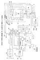
図3は本発明の半導体記憶装置の第1実施形態の要部を示す回路図であり、本発明の半導体記憶装置の第1実施形態は、図1に示すDRAM1に使用することができるものである。
【0027】
図3中、5はコントローラからのコマンド信号を入力してデコードするコマンドデコーダ、6はコントローラからのアドレス信号A0〜Anを入力してラッチするアドレス入力回路、7はライトデータ/リードデータDQ0〜DQnの入出力を行うデータ入出力回路である。
【0028】
また、8はリフレッシュを自己管理するリフレッシュ制御回路、9はリフレッシュ制御回路8に制御されてビジー信号BUSY1を出力するBUSY1出力回路、10はリフレッシュ制御回路8に制御されてリフレッシュアドレスを出力するリフレッシュカウンタである。
【0029】
また、11−0、11−1はバンクアドレス信号により選択されるバンク(BANK)と呼ばれるメモリ領域であり、バンク11−0、11−1は同一回路構成とされており、バンク11−0において、12−0〜12−3はブロックと呼ばれるメモリ領域である。
【0030】
ブロック12−0〜12−3は同一回路構成とされており、ブロック12−0において、13はメモリセルが配列されてなるメモリセルアレイ、14はロウアドレス信号をデコードしてワード線の選択を行うロウデコーダ、15はメモリセルアレイ13からのリードデータの増幅を行うセンスアンプ、16はコラムアドレス信号をデコードしてコラムの選択を行うコラムデコーダである。
【0031】
また、17はブロック12−0〜12−3により共有されるデータバス、18はブロック12−0〜12−3により共有されるライトアンプ/センスバッファ、19はバンク11−0の動作を制御する制御回路である。
【0032】
また、20は制御回路19に制御されて、リード/ライト時には、アドレス入力回路6から出力されるロウアドレス信号を選択し、リフレッシュ時には、リフレッシュカウンタ10から出力されるリフレッシュアドレスを選択するセレクタ、21はセレクタ20から出力されるアドレス信号をラッチするアドレスラッチ回路である。
【0033】
図4はリフレッシュ制御回路8、BUSY1出力回路9及びリフレッシュカウンタ10の構成を示す回路図であり、図4中、Comは外部からコマンド信号をデコードしてなる内部コマンド信号、23はバンク11−1が備える制御回路、RASzはラス系の回路を活性化するラス系活性化信号であり、本発明の半導体記憶装置の第1実施形態では、リフレッシュは、各ロウアドレスごとに、バンク11−0、11−1の順に交互に行われるものとする。
【0034】
また、リフレッシュ制御回路8において、24は定期的にリフレッシュ時期を知らせるリフレッシュ制御信号Ref1を発生するRef1発生回路であり、リフレッシュ時期の管理は、本発明の半導体記憶装置の第1実施形態の内部にオシレータを搭載して時間を測定することにより行うようにしても良いし、あるいは、本発明の半導体記憶装置の第1実施形態を使用する電子装置に備えられる水晶発振器等からのクロック信号を利用して時間を測定することにより行うようにしても良い。
【0035】
また、25はビジー信号BUSY1の出力とコントローラからのコマンドの出力とが同時に行われた場合に、コマンドの実行を優先するために、リフレッシュカウンタ10の動作開始をコマンドの実行が終了するまで遅延させるためのリフレッシュ制御信号Refzを発生するRefz発生回路である。
【0036】
また、26はコマンドデコーダ5から出力される内部コマンド信号Comとリフレッシュ制御信号Ref1とをNAND処理するNAND回路、27はNAND回路26の出力S26によりON、OFFが制御されるNMOSトランジスタである。
【0037】
また、28はNMOSトランジスタ27を介して供給されるリフレッシュ制御信号Ref1とリフレッシュ制御信号RefzとをNOR処理するNOR回路、29はNOR回路28の出力を反転してリフレッシュ制御信号REFを出力するインバータである。
【0038】
また、リフレッシュカウンタ10において、30はリフレッシュ制御信号REFをトリガ信号としてカウント動作を開始してリフレッシュアドレスを出力するカウンタ、31はカウンタ30の出力をNAND処理するNAND回路、32はNAND回路31の出力を反転してリフレッシュの終了を知らせるリフレッシュ終了信号Ref−endを出力するインバータである。
【0039】
また、BUSY1出力回路9において、33はリフレッシュ制御信号Ref1をセット信号、リフレッシュ終了信号Ref−endをリセット信号として入力されるRSフリップフロップ回路、34はRSフリップフロップ回路33の正相出力Qを反転してビジー信号BUSY1を出力するインバータである。
【0040】
図5はRefz発生回路25の構成を示す回路図であり、図5中、36、37はフリップフロップ回路を構成するNAND回路、38はNAND回路36の出力を反転遅延する反転遅延回路であり、39はインバータ、40は抵抗、41はキャパシタである。また、42はNAND回路36の出力と反転遅延回路38の出力とをNOR処理してリフレッシュ制御信号Refzを出力するNOR回路である。
【0041】
図6はリフレッシュ制御回路8、BUSY1出力回路9及びリフレッシュカウンタ10の第1動作例を示す波形図であり、図6Aはコントローラから出力されるコマンド、図6Bはリフレッシュ制御信号Ref1、図6Cはビジー信号BUSY1、図6Dは内部コマンド信号Com、図6Eはラス系活性化信号RASz、図6Fはリフレッシュ制御信号REF、図6Gはカウンタ30の出力を示している。
【0042】
図6はコントローラからコマンドが出力されていないときに、Ref1発生回路24からリフレッシュ制御信号Ref1が出力された場合(リフレッシュ制御信号Ref1がHレベルとされた場合)を示している。
【0043】
この場合には、まず、リセットされていたRSフリップフロップ回路33がリフレッシュ制御信号Ref1によりセットされ、RSフリップフロップ回路33の正相出力Q=Hレベルとなり、ビジー信号BUSY1が出力される(ビジー信号BUSY1=Lレベルとなる)。
【0044】
また、この場合には、内部コマンド信号Com=Lレベル、NAND回路26の出力S26=Hレベルとなり、NMOSトランジスタ27=ONとなると共に、ラス系活性化信号RASz=Lレベルとなり、Refz発生回路25においては、NAND回路37の出力=Hレベル、NAND回路36の出力=Lレベル、反転遅延回路38の出力=Hレベル、リフレッシュ制御信号Refz=Lレベルとなる。
【0045】
この結果、Ref1発生回路24から出力されるリフレッシュ制御信号Ref1は、NMOSトランジスタ27を介して、NOR回路28に供給されるが、NOR回路28は、リフレッシュ制御信号Ref1に対してインバータとして機能することになるので、リフレッシュ制御信号REFとして、リフレッシュ制御信号Ref1が出力され、カウンタ30が起動される。
【0046】
すなわち、コントローラからコマンドが出力されていないときに、Ref1発生回路24からリフレッシュ制御信号Ref1が出力された場合には、ビジー信号BUSY1がLレベルにされた後、直ちに、カウンタ30からリフレッシュアドレスが出力されリフレッシュが実行されることになる。
【0047】
その後、リフレッシュアドレスが全て出力され、カウンタ30の出力が全てHレベルになると、NAND回路31の出力=Lレベル、リフレッシュ終了信号Ref−end=Hレベルとなり、RSフリップフロップ回路33はリセットされ、RSフリップフロップ回路33の正相出力Q=Lレベル、ビジー信号BUSY1=Hレベルとなり、ビジー信号BUSY1は解除される。
【0048】
図7はリフレッシュ制御回路8、BUSY1出力回路9及びリフレッシュカウンタ10の第2動作例を示す波形図であり、図7Aはコントローラから出力予定のコマンド、図7Bはコントローラから実際に出力されるコマンド、図7Cはリフレッシュ制御信号Ref1、図7Dはビジー信号BUSY1、図7Eは内部コマンド信号Com、図7Fはラス系活性化信号RASz、図7GはNAND回路26の出力S26、図7Hリフレッシュ制御信号Refz、図7Iはリフレッシュ制御信号REF、図7Jはカウンタ30の出力を示している。
【0049】
図7はコントローラからのコマンドの入力とリフレッシュ制御信号Ref1の出力とが同時であった場合を示している。具体的には、コントローラからコマンドC1、C2、C3が連続して出力される予定であった場合において、コマンドC1の入力とリフレッシュ制御信号Ref1の出力とが同時であった場合を示している。
【0050】
この場合には、まず、リセットされていたRSフリップフロップ回路33がリフレッシュ制御信号Ref1によりセットされ、RSフリップフロップ回路33の正相出力Q=Hレベルとなり、ビジー信号BUSY1が出力される(ビジー信号BUSY1=Lレベルとなる)。
【0051】
また、この場合には、内部コマンド信号Com=Hレベル、NAND回路26の出力=Lレベルとなり、NMOSトランジスタ27=OFFとなるので、リフレッシュ制御信号Ref1がNOR回路28に供給されることはない。
【0052】
そして、その後、リフレッシュ制御信号Ref1がLレベルになると、NAND回路26の出力S26=Hレベル、NMOSトランジスタ27=ONとなり、NOR回路28はリフレッシュ制御信号Refzに対してインバータとして機能することになり、この場合には、リフレッシュ制御信号REFとして、リフレッシュ制御信号Refzが出力されることになる。
【0053】
また、内部コマンド信号Com=Hレベル、NAND回路26の出力S26=Lレベルとなることにより、Refz発生回路25においては、NAND回路36の出力=Hレベル、リフレッシュ制御信号Refz=Lレベルになり、その後、反転遅延回路38の出力=Hレベルとなり、リフレッシュ制御信号Refz=Lレベルが維持される。
【0054】
また、内部コマンド信号Com=Hレベルとなることにより、ラス系活性化信号RASz=Hレベルとなるが、コマンドC1の実行が終了すると、ラス系活性化信号RASz=Lレベルとなり、この結果、Refz発生回路25においては、NAND回路37の出力=Hレベル、NAND回路36の出力=Lレベルとなり、リフレッシュ制御信号Refz=Hレベルとなり、その後、反転遅延回路38の出力=Hレベルとなることによりリフレッシュ制御信号Refz=Lレベルとなる。
【0055】
したがって、コマンドC1の入力とリフレッシュ制御信号Ref1の出力とが同時であった場合には、ビジー信号BUSY1がLレベルにされるが、コマンドC1の実行が終了した後、カウンタ30からリフレッシュアドレスが出力され、リフレッシュが実行されることになる。
【0056】
そして、その後、リフレッシュアドレスが全て出力され、カウンタ30の出力が全てHレベルになると、NAND回路31の出力=Lレベル、リフレッシュ終了信号Ref−end=Hレベルとなり、RSフリップフロップ回路33は、リフレッシュ終了信号Ref−endによりリセットされ、RSフリップフロップ回路33の正相出力Q=Lレベル、ビジー信号BUSY1=Hレベルとなり、ビジー信号BUSY1は解除される。
【0057】
このように、本発明の半導体記憶装置の第1実施形態では、コントローラからのコマンドの入力とリフレッシュ制御信号Ref1の出力とが同時であった場合には、コマンドの実行が優先され、コマンドの実行の後、リフレッシュが行われることになる。
【0058】
図8はコマンドデコーダ5の構成を示す回路図であり、図8中、44はコントローラからのコマンド信号をバッファリングする入力バッファ、45はビジー信号BUSY1を反転するインバータである。
【0059】
また、46−0、46−mは入力バッファ44から出力されるコマンドの伝送を制御する伝送ゲートの一部であり、47−0、47−mはビジー信号BUSY1によりON、OFFが制御されるNMOSトランジスタ、48−0、48−mはインバータ45の出力によりON、OFFが制御されるPMOSトランジスタである。なお、伝送ゲート46−0、46−m間に存在する伝送ゲート46−1〜46−(m−1)は図示を省略している。
【0060】
伝送ゲート46−0〜46−mは、ビジー信号BUSY1=Hレベルの場合にはON、ビジー信号BUSY1=Lレベルの場合にはOFFとされるものであり、リフレッシュ期間中に、仮に、コントローラからコマンドが出力されたとして、コマンド信号の取り込みが行われることはない。
【0061】
また、49は入力バッファ44から伝送ゲート46−0〜46−mを介して供給されるコマンド信号をデコードして内部コマンド信号Comを出力するコントロールデコーダである。
【0062】
図9はアドレス入力回路6の構成を示す回路図であり、図9中、51はコントローラからのアドレス信号A0〜Anをバッファリングする入力バッファ、52はビジー信号BUSY1を反転するインバータである。
【0063】
また、53−0、53−nは入力バッファ51から出力されるアドレス信号A0〜Anの伝送を制御する伝送ゲートの一部であり、54−0〜54−nはビジー信号BUSY1によりON、OFFが制御されるNMOSトランジスタ、55−0、55−nはインバータ52の出力によりON、OFFが制御されるPMOSトランジスタである。なお、伝送ゲート53−0、53−n間に存在する伝送ゲート53−1〜53−(n−1)は図示を省略している。
【0064】
伝送ゲート53−0〜53−nは、ビジー信号BUSY1=Hレベルの場合にはON、ビジー信号BUSY1=Lレベルの場合にはOFFとされるものであり、リフレッシュ期間中に、仮に、コントローラからアドレス信号A0〜Anが出力されても、アドレス信号A0〜Anの取り込みが行われることはない。また、56は入力バッファ51から伝送ゲート53−0〜53−nを介して供給されるアドレス信号A0〜Anをラッチするアドレスラッチ回路である。
【0065】
このように、本発明の半導体記憶装置の第1実施形態によれば、リフレッシュ制御回路8によりリフレッシュを自己管理し、リフレッシュ時期になると、処理中のコマンドがない場合は直ちに、処理中のコマンドがある場合にはコマンド実行後、リフレッシュカウンタ10から出力されるリフレッシュアドレスに基づいてリフレッシュを行うことができるように構成されているので、コントローラによるリフレッシュ管理が不必要となる。
【0066】
また、本発明の半導体記憶装置の第1実施形態によれば、リフレッシュ時期になると、BUSY1出力回路9からビジー信号BUSY1を出力するように構成されているので、コントローラは、ビジー信号BUSY1を受信することにより、本発明の半導体記憶装置の第1実施形態がリフレッシュ期間にあることを知ることができるので、コントローラによるアクセス制御が容易となる。
【0067】
更に、本発明の半導体記憶装置の第1実施形態によれば、コマンドの入力とビジー信号BUSY1の出力とが同時の場合には、コマンドの実行を優先するように構成されているので、コントローラは、コマンドの入力とビジー信号BUSY1の出力とが同時の場合であっても、このコマンドを再び出力する必要がなく、この点からも、コントローラによるアクセス制御が容易となる。
【0068】
なお、本発明の半導体記憶装置の第1実施形態によれば、ビジー信号BUSY1の出力中は、コマンドデコーダ5はコマンドの取り込みを行わないように制御されると共に、アドレス入力回路6はアドレス信号を取り込まないように制御されるので、コントローラは、図10に示すように、ビジー信号BUSY1が出力されている間は、本発明の半導体記憶装置の第1実施形態に取り込まれなかったコマンドを繰り返して出力するようにしても良い。
【0069】
本発明の半導体記憶装置の第2実施形態・・図11〜図14
図11は本発明の半導体記憶装置の第2実施形態の要部を示す回路図である。本発明の半導体記憶装置の第2実施形態は、図1に示すDRAM1に使用することができるものである。
【0070】
本発明の半導体記憶装置の第2実施形態は、図3に示す本発明の半導体記憶装置の第1実施形態が設けていないBUSY1a発生回路58及びBUSY1b発生回路59を設けると共に、図3に示す本発明の半導体記憶装置の第1実施形態が設けるコマンドデコーダ5及びアドレス入力回路6と回路構成の異なるコマンドデコーダ60及びアドレス入力回路61を設け、その他については、図3に示す本発明の半導体記憶装置の第1実施形態と同様に構成したものである。
【0071】
BUSY1b発生回路59は、ビジー信号BUSY1を入力して、ビジー信号BUSY1bを出力するものであり、ビジー信号BUSY1bは、図14Eに示すように、ビジー信号BUSY1がLレベルからHレベルに変化した場合に、HレベルからLレベルに変化し、その後、一定期間経過後にHレベルに変化するものである。
【0072】
BUSY1a発生回路58は、ビジー信号BUSY1、BUSY1bを入力して、ビジー信号BUSY1aを出力するものであり、ビジー信号BUSY1aは、図14Dに示すように、ビジー信号BUSY1がHレベルからLレベルに変化した場合に、HレベルからLレベルに変化し、その後、ビジー信号BUSY1bがLレベルからHレベルに変化した場合に、LレベルからHレベルに変化するものである。
【0073】
図12はコマンドデコーダ60の構成を示す回路図である。図12中、63はコントローラからのコマンド信号をバッファリングする入力バッファ、64はコマンド信号をデコードして内部コマンド信号Comを出力するコントロールデコーダ、65はコマンド信号を一時保管するレジスタである。
【0074】
また、66はビジー信号BUSY1aにより動作が制御される切換えスイッチ回路であり、ビジー信号BUSY1a=Hレベルの場合には、入力バッファ63から出力されるコマンド信号をコントロールデコーダ64に伝送し、ビジー信号BUSY1a=Lレベルの場合には、入力バッファ63から出力されるコマンド信号をレジスタ65に供給するものである。
【0075】
また、67はビジー信号BUSY1bにより動作が制御される接続スイッチ回路であり、ビジー信号BUSY1b=Lレベルの場合にはONとなり、レジスタ65に一時保管されているコマンド信号をコントロールデコーダ64に供給し、ビジー信号BUSY1b=Hレベルの場合にはOFFとなるものである。
【0076】
図13はアドレス入力回路61の構成を示す回路図である。図13中、69はコントローラからのアドレス信号A0〜Anをバッファリングする入力バッファ、70はアドレス信号A0〜Anをラッチするアドレスラッチ回路、71はアドレス信号A0〜Anを一時保管するレジスタである。
【0077】
また、72はビジー信号BUSY1aにより動作が制御される切換えスイッチ回路であり、ビジー信号BUSY1a=Hレベルの場合には、入力バッファ69から出力されるアドレス信号A0〜Anをアドレスラッチ回路70に伝送し、ビジー信号BUSY1a=Lレベルの場合には、入力バッファ69から出力されるアドレス信号A0〜Anをレジスタ71に供給するものである。
【0078】
また、73はビジー信号BUSY1bにより動作が制御される接続スイッチ回路であり、ビジー1信号BUSY1=Lレベルの場合にはONとなり、レジスタ71に一時保管されているアドレス信号A0〜Anをアドレスラッチ回路70に供給し、ビジー信号BUSY1b=Hレベルの場合にはOFFとなるものである。
【0079】
図14は本発明の半導体記憶装置の第2実施形態の動作を示す波形図であり、図14Aはコントローラから出力されるコマンド、図14Bはリフレッシュ制御信号Ref1、図14Cはビジー信号BUSY1、図14Dはビジー信号BUSY1a、図14Eはビジー信号BUSY1b、図14Fはコマンドデコーダ60の入力バッファ63の出力、図14Gはコマンドデコーダ60のレジスタ65の出力、図14Hはラス系活性化信号RASzを示している。
【0080】
図14はコントローラからコマンドC1が出力された後、リフレッシュ制御回路8のRef1発生回路24からリフレッシュ制御信号Ref1が出力され、これに応じて、BUSY1出力回路9からビジー信号BUSY1が出力されたが、コントローラからコマンドC1に続いてコマンドC2が出力された場合を示している。
【0081】
この場合、コマンドC1は、コマンドデコーダ60において、入力バッファ63及び切換えスイッチ回路66を介してコントローラデコーダ64に伝送されてデコードされ、コマンドC1が実行される。
【0082】
また、図14Bに示すように、リフレッシュ制御回路8のRef1発生回路24からリフレッシュ制御信号Ref1が出力されることにより、図14Cに示すように、BUSY1出力回路9からビジー信号BUSY1が出力され(ビジー信号BUSY1がLレベルとされ)、コマンドC1の実行後、リフレッシュが行われる。
【0083】
他方、ビジー信号BUSY1がLレベルに変化することを受けてビジー信号BUSY1aがHレベルからLレベルに変化し、コントローラから出力されるコマンドC2は、コマンドデコーダ60において、入力バッファ63及び切換えスイッチ回路66を介してレジスタ65に一時保管される。
【0084】
そして、リフレッシュが終了し、ビジー信号BUSY1がLレベルからHレベルに変化すると(ビジー信号BUSY1が解除されると)、これを受けて、ビジー信号BUSY1bがHレベルからLレベルに変化し、コマンドデコーダ60のレジスタ65に一時保管されているコマンドC2が接続スイッチ回路67を介してコントローラデコーダ64に供給されてデコードされ、コマンドC2が実行される。
【0085】
本発明の半導体記憶装置の第2実施形態によれば、リフレッシュ制御回路8によりリフレッシュを自己管理し、リフレッシュ時期になると、処理中のコマンドがない場合は直ちに、処理中のコマンドがある場合にはコマンド実行後、リフレッシュカウンタ10から出力されるリフレッシュアドレスに基づいてリフレッシュを行うことができるように構成されているので、コントローラによるリフレッシュ管理が不必要となる。
【0086】
また、本発明の半導体記憶装置の第2実施形態によれば、リフレッシュ時期になると、BUSY1出力回路9からビジー信号BUSY1を出力するように構成されているが、リフレッシュ中であっても、コマンド信号及びアドレス信号を受け付けることができるので、コントローラは、本発明の半導体記憶装置の第2実施形態がリフレッシュ中であっても、本発明の半導体記憶装置の第2実施形態にアクセスすることができ、効率的な動作を行うことができる。
【0087】
本発明の電子装置の第2実施形態・・図15
図15は本発明の電子装置の第2実施形態の要部を示す回路図であり、本発明の電子装置の第2実施形態は、図1に示す本発明の電子装置の第1実施形態が設けるコントローラ2と回路構成の異なるコントローラ75を設け、その他については、本発明の電子装置の第1実施形態と同様に構成したものである。
【0088】
コントローラ75は、DRAM1(図3に示す本発明の半導体記憶装置の第1実施形態又は図11に示す本発明の半導体記憶装置の第2実施形態等)が備えるリフレッシュカウンタ10と同様のリフレッシュカウンタ76を設け、DRAM1からのビジー信号BUSY1を受信するごとに、リフレッシュカウンタ76を起動し、DRAM1がリフレッシュしているアドレスを確認することができるようにしたものである。
【0089】
そこで、DRAM1として、たとえば、図3に示す本発明の半導体記憶装置の第1実施形態又は図11に示す本発明の半導体記憶装置の第2実施形態を使用する場合、バンク11−0、11−1を独立で動作させるようにし、一方のバンクがリフレッシュ中でも、他方のバンクは、リード/ライトを行うことができるようにしておけば、コントローラ75は、リフレッシュ中のバンクを避けて、他のバンクをアクセスすることが可能となる。
【0090】
このように構成された本発明の電子装置の第2実施形態によれば、図1に示す本発明の電子装置の第1実施形態と同様の作用効果を得ることができると共に、コントローラ75は、DRAM1内のリフレッシュ中以外のバンクにアクセスすることができるので、動作の効率化を図ることができる。
【0091】
本発明の電子装置の第3実施形態・・図16
図16は本発明の電子装置の第3実施形態の要部を示す回路図であり、図16中、78はDRAM、79はDRAM78を制御するコントローラ、80はコマンドバス、アドレスバス及びデータバス等のバスである。
【0092】
DRAM78は、リフレッシュを自己管理し、リフレッシュの時期になると、内部でリフレッシュアドレスを発生してリフレッシュを開始し、リフレッシュ中にコントローラ79からコマンドが出力されたときは、このコマンドを入力し、リフレッシュ中にメモリセルからビット線に出力されたデータを所定の内部回路に待避させてリフレッシュを中断し、入力したコマンドを実行し、その後、待避したデータをビット線に戻してリフレッシュを再開するように構成したものである。
【0093】
本発明の電子装置の第3実施形態によれば、DRAM78は、リフレッシュを自己管理し、リフレッシュ時期になると、内部でリフレッシュアドレスを発生してリフレッシュを実行するように構成されているので、コントローラ79によるDRAM78のリフレッシュ管理が不必要である。
【0094】
また、DRAM78は、リフレッシュ中にコントローラ79からコマンドが出力された場合、リフレッシュを中断して、コントローラ79から出力されたコマンドを実行し、その後、リフレッシュを再開するように構成されているので、コントローラ79は、DRAM78がリフレッシュ中であるか否かを判断することなく、DRAM78にアクセスすることができる。
【0095】
したがって、本発明の電子装置の第3実施形態を携帯電話等の簡易端末に適用し、携帯電話などの簡易端末にリフレッシュを必要とするDRAMを搭載するようにしても、コントローラによるDRAMの制御を容易に行うことができる。
【0096】
本発明の半導体記憶装置の第3実施形態・・図17〜図32
図17は本発明の半導体記憶装置の第3実施形態の要部を示す回路図であり、本発明の半導体記憶装置の第3実施形態は、図16に示すDRAM78に使用することができるものである。
【0097】
図17中、82はコントローラからのコマンド信号をデコードするコマンドデコーダ、83はコントローラからのアドレス信号A0〜Anを入力するアドレス入力回路、84はライトデータ/リードデータDQ0〜DQnの入出力を行うデータ入出力回路である。
【0098】
また、85はリフレッシュを自己管理し、定期的にリフレッシュ制御信号REFを出力するリフレッシュ制御回路、86はリフレッシュ制御信号REFをトリガ信号としてリフレッシュアドレスを出力するリフレッシュカウンタ、87はアドレス入力回路83から出力されるロウアドレスとリフレッシュカウンタ86から出力されているリフレッシュアドレスとを比較する比較器である。
【0099】
また、88−0、88−1はバンクアドレス信号により選択されるバンクであり、バンク88−0、88−1は同一回路構成とされており、バンク88−0において、89−0〜89−3はブロックである。ブロック89−0〜89−3は同一回路構成とされており、ブロック89−0において、90はメモリセルアレイ、91はロウデコーダ、92はセンスアンプ、93はコラムデコーダである。
【0100】
また、94はリフレッシュ時にビット線にリード途中のデータを一時的に格納するためのデータレジスタ、95はビット線とデータレジスタとの接続を図る転送ゲート、96は転送ゲートのON、OFFを制御する転送ゲート信号を発生する転送ゲート信号発生回路である。
【0101】
また、97はブロック89−0〜89−3により共有されるデータバス、98はブロック89−0〜89−3により共有されるライトアンプ/センスバッファ、99はバンク88−0の動作を制御する制御回路である。
【0102】
また、100は制御回路99に制御されて、リード/ライト時には、アドレス入力回路83から出力されるロウアドレス信号を選択し、リフレッシュ時には、リフレッシュカウンタ86から出力されるリフレッシュアドレスを選択するセレクタ、101はセレクタ100から出力されるアドレス信号をラッチするアドレスラッチ回路である。
【0103】
図18はデータレジスタ94及び転送ゲート95の構成を示す回路図である。図18中、BL0、/BL0、BLx、/BLxはビット線、103−0、103−xはフリップフロップ、104−0、104−x、105−0、105−xはインバータ、106−0、106−x、107−0、107−xは転送ゲート信号によりON、OFFが制御されるNMOSトランジスタである。
【0104】
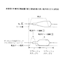
図19、図20は本発明の半導体記憶装置の第3実施形態の第1、第2動作例を従来のDRAMの場合との比較で示す波形図であり、図19A、図20Aは従来のDRAMの動作例、図19Bは本発明の半導体記憶装置の第3実施形態の第1動作例、図20Bは本発明の半導体記憶装置の第3実施形態の第2動作例を示している。
【0105】
これら動作例は、ワード線WL0により選択されているメモリセルのリフレッシュ中に、ワード線WL1により選択されるメモリセルに対するアクセスがあった場合を示しており、従来のDRAMの場合には、ワード線WL0により選択されているメモリセルのリフレッシュ中には、ワード線WL1により選択されるメモリセルのリード又はライトを行うことができないので、図19A及び図20Aに示すように、ワード線WL0により選択されているメモリセルのリフレッシュが終了してから、ワード線WL1により選択されるメモリセルのリード又はライトを行うことになる。
【0106】
これに対して、本発明の半導体記憶装置の第3実施形態の第1動作例の場合においては、図19Bに示すように、ワード線WL0により選択されるメモリセルのリフレッシュが開始されると、センスアンプによるビット線BL、/BL間の電位差の拡大途中に、転送ゲート信号がHレベルとされ、ビット線BL、/BLに出力されているメモリセルのデータD0がデータレジスタ94に待避され、ワード線WL0が非選択とされ、かつ、転送ゲート信号がLレベルとされる。
【0107】
そして、ワード線WL1が選択されて、リード又はライトが行われ、その後、ワード線WL1が非選択とされ、リード又はライトが終了すると、転送ゲート信号がHレベルとなり、転送ゲート95がONとされ、データレジスタ94に格納されているデータがビット線BL、/BLに転送されると共に、ワード線WL0が再び選択され、ワード線WL0により選択されるメモリセルのリフレッシュが再開される。
【0108】
また、本発明の半導体記憶装置の第3実施形態の第2動作例の場合においては、図20Bに示すように、ワード線WL0により選択されるメモリセルのリフレッシュが開始されると、センスアンプによりビット線BL、/BL間の電位差が拡大される前に、すなわち、メモリセルによりビット線BL、/BL間に電位差が発生した段階で、転送ゲート信号がHレベルとされ、ビット線BL、/BLに出力されているメモリセルのデータD0がデータレジスタ94に待避され、転送ゲート信号がLレベルにされ、更に、ワード線WL0が非選択とされる。
【0109】
そして、ワード線WL1が選択されて、リード又はライトが行われ、その後、ワード線WL1が非選択とされ、リード又はライトが終了すると、転送ゲート信号がHレベルとなり、転送ゲート95がONとされ、データレジスタ94に格納されているデータがビット線BL、/BLに転送されると共に、ワード線WL0が選択され、ワード線WL0により選択されるメモリセルのリフレッシュが再開される。なお、本発明の半導体記憶装置の第3実施形態の第2動作例は、本発明の半導体記憶装置の第3実施形態の第1動作例の場合よりもワード線WL1のリード又はライト動作を高速化したものである。
【0110】
このように、本発明の半導体記憶装置の第3実施形態では、リフレッシュ中に外部からアクセスがあると、リフレッシュは、リフレッシュ途中時のビット線BL、/BL上のデータをデータレジスタ94に待避させるリフレッシュステップ1と、外部からのアクセスに基づくコマンドの実行が終了した後にデータレジスタ94に格納されているデータをビット線BL、/BLに転送してリフレッシュを再開するリフレッシュステップ2の2個のステップにより実行される。
【0111】
図21は本発明の半導体記憶装置の第3実施形態の第3動作例を示すタイムチャートであり、本発明の半導体記憶装置の第3実施形態の第3動作例は、リフレッシュステップ1と、リフレッシュステップ2との間に、複数のワード線を順に選択し、これら複数のワード線により選択されるメモリセルのリード又はライトを行うというものである。
【0112】
図22は本発明の半導体記憶装置の第3実施形態の第4動作例を示す波形図であり、ワード線WL0のリフレッシュ時に、外部からアクセスがなかった場合を示している。この場合、リフレッシュは、リフレッシュステップ1、2を連続することにより実行される。なお、この場合には、リフレッシュステップ2における転送ゲートのON動作は行わないようにした方が好適である。
【0113】
図23は本発明の半導体記憶装置の第3実施形態の第5動作例及び第6動作例を示すタイムチャートであり、図23Aは第5動作例、図23Bは第6動作例を示している。
【0114】
ここに、本発明の半導体記憶装置の第3実施形態の第5動作例は、ワード線WL0をリフレッシュのために選択中に、コントローラからワード線WL0に対するアクセスがあった場合を示しており、この場合には、リフレッシュステップ1及びリフレッシュステップ2が連続して行われ、そして、リフレッシュステップ2から引き続きワード線WL0により選択されるメモリセルのリード又はライトが行われるというものである。
【0115】
この動作は、比較器87において、アドレス入力回路83から出力されるロウアドレスとリフレッシュカウンタ86から出力されるリフレッシュアドレスとを比較し、アドレス入力回路83から出力されるロウアドレスとリフレッシュカウンタ86から出力されているリフレッシュアドレスとが一致しているときに行われるものであり、このようにすることにより、リフレッシュ中のメモリセルからのデータのリード又はライトを行うことが可能となる。
【0116】
また、本発明の半導体記憶装置の第3実施形態の第6動作例は、ワード線WL0をリフレッシュのために選択中に、コントローラからワード線WL1、WL0に対するアクセスが連続してあった場合を示しており、この場合には、リフレッシュステップ1が行われた後、ワード線WL1により選択されるメモリセルのリード又はライトが行われ、続いて、リフレッシュステップ2が行われ、そして、リフレッシュステップ2から引き続きワード線WL0により選択されるメモリセルのリード又はライトが行われるというものである。
【0117】
この動作は、比較器87において、アドレス入力回路83から出力されるロウアドレスとリフレッシュカウンタ86から出力されるリフレッシュアドレスとを比較し、アドレス入力回路83から出力されるロウアドレスとリフレッシュカウンタ86から出力されているリフレッシュアドレスとが一致していないときに行われるものであり、このようにすることにより、リフレッシュ中のメモリセルからのデータのリード又はライトを行うことが可能となる。
【0118】
図24は本発明の半導体記憶装置の第7動作例を説明するための波形図であり、リフレッシュが開始された初期の段階で、データレジスタ94へのデータ転送が終了されるまでの期間をリフレッシュ中断禁止期間、それ以降をリフレッシュ中断可能期間とし、リフレッシュを中断してリード又はライトを行う場合に必要とするプリチャージ期間をリフレッシュを中断した時点により調整するというものである。
【0119】
すなわち、図25に示すように、リフレッシュ中断禁止期間以降は、プリチャージが始まるまでのどの時点(たとえば、P1、P2、P3)でもリフレッシュ中断が可能であるが、リフレッシュ中断後のプリチャージに必要な期間は、ビット線の開き幅、すなわち、リフレッシュが中断された時点により異なることになる。
【0120】
たとえば、P1、P2又はP3でリフレッシュが中断された場合、あるいは、リフレッシュが中断されなかった場合、プリチャージに必要な時間は、P1で中断された場合、P2で中断された場合、P3で中断された場合、リフレッシュが中断されなかった場合の順に長くなる。
【0121】
このように、リフレッシュ中断が早い場合は、その後に続く、プリチャージ期間は短くてすみ、次のリード又はライトを早く開始できるので、これを達成することができるプリチャージ信号発生回路を備えることが好適である。
【0122】
図26は本発明の半導体記憶装置の第3実施形態が備えるプリチャージ信号発生回路の構成を示す回路図である。図26中、109、110はフリップフロップ回路を構成するNAND回路、111、112はインバータ、113はプリチャージ信号の長さ、すなわち、プリチャージ期間を制御するプリチャージ期間制御回路である。
【0123】
図27はプリチャージ期間制御回路113の構成を示す回路図である。図27中、115は可変遅延回路、116は可変遅延回路115の遅延時間を制御する遅延時間制御信号SD1〜SD4を出力する遅延時間制御回路であり、遅延回路115において、117、118はインバータ、119〜122は遅延時間制御信号SD1〜SD4によりON、OFFが制御されるNMOSトランジスタ、123〜126はキャパシタである。
【0124】
図28は遅延時間制御回路116の構成を示す回路図である。図28中、128はラス系活性化信号RASzを入力してリセット信号S1を出力するリセット信号発生回路、129はリフレッシュ中断禁止期間になるとHレベルとなるリフレッシュ中断禁止信号K1及び内部コマンド信号Comを入力してリフレッシュ時間測定信号S3を発生するリフレッシュ時間測定信号発生回路である。
【0125】
また、130〜133は遅延回路であり、134〜141はインバータ、142〜145はキャパシタである。これら遅延回路130〜133の合計遅延時間はリフレッシュ中断可能期間となるように、遅延回路130〜133の遅延時間が設定される。
【0126】
また、146はリフレッシュ時間測定信号S3を反転するインバータ、147〜150はPMOSトランジスタ及びNMOSトランジスタからなる転送ゲートであり、リフレッシュ時間測定信号S3=Hレベル、インバータ146の出力=Lレベルの場合にON、リフレッシュ時間測定信号S3=Lレベル、インバータ146の出力=Hレベルの場合にOFFとされるものである。
【0127】
また、151〜154は遅延回路130〜133の出力SD11〜SD14をラッチするラッチ回路、155〜158はラッチ回路151〜154の出力を反転して遅延時間制御信号SD1〜SD4を出力するインバータである。
【0128】
また、159〜162はラッチ回路151〜154をリセットするリセット用のPMOSトランジスタであり、リセット信号S1によりON、OFFが制御され、リセット信号S1=Lレベルの場合にON、リセット信号S1=HLレベルの場合にOFFとされるものである。
【0129】
図29はリセット信号発生回路128の構成を示す回路図である。図29中、164〜166はラス系活性化信号RASzを反転遅延する反転遅延回路を構成するインバータ、167はラス系活性化信号RASzとインバータ166の出力とをNAND処理してリセット信号S1を出力するNAND回路である。
【0130】
図30はリフレッシュ時間測定信号発生回路129の構成を示す回路図であり、図30中、170〜172はリフレッシュ中断禁止信号K1を反転遅延する反転遅延回路を構成するインバータ、173はリフレッシュ中断禁止信号K1とインバータ172の出力とをNOR処理するNOR回路、174、175はNOR回路173の出力と内部コマンド信号Comとを入力とするフリップフロップ回路を構成するNOR回路、176はNOR回路174の出力を反転してリフレッシュ時間測定信号S3を出力するインバータである。
【0131】
図31は遅延時間制御回路116の動作を示す波形図であり、図31Aはラス系活性化信号RASz、図31Bはリセット信号S1、図31Cはリフレッシュ中断禁止信号K1、図31Dはリフレッシュ時間測定信号発生回路129のNOR回路173の出力S2、図31Eは内部コマンド信号Com、図31Fはリフレッシュ時間測定信号S3、図31Gは遅延回路130の出力SD11、図31Hは遅延回路131の出力SD12、図31Iは遅延回路132の出力SD13、図31Jは遅延回路133の出力SD14を示している。
【0132】
ここに、リフレッシュを行うために、ラス系活性化信号RASzがLレベルからHレベルに立ち上がると、リセット信号発生回路128からLレベルのリセット信号S1が出力され、PMOSトランジスタ159〜162=ON、ラッチ回路151〜154の出力=Lレベル、遅延時間制御信号SD1〜SD4=Hレベルとされる。
【0133】
また、リフレッシュ中断禁止期間になると、Hレベルからなるリフレッシュ中断禁止信号K1が出力され、リフレッシュ時間測定信号発生回路129のNOR回路173の出力S2は、一時的にHレベルとなり、この結果、リフレッシュ時間測定信号S3=Hレベルとなり、これが遅延回路130〜133により遅延されると共に、転送ゲート147〜150はONとなる。
【0134】
その後、たとえば、遅延回路130、131の出力SD11、SD12がHレベル、遅延回路132、133の出力SD13、SD14がLレベルのときに、コマンド信号Comが出力されると、転送ゲート147〜150=OFFとなり、ラッチ回路151〜154は、遅延回路130〜133の出力SD11〜SD14をラッチすることになる。
【0135】
この結果、この場合には、ラッチ回路151、152の出力=Lレベル、ラッチ回路153、154の出力=Hレベル、遅延時間制御信号SD1、SD2=Hレベル、遅延時間制御信号SD3、SD4=Lレベルとなり、遅延時間はキャパシタ123、124の分だけとなる。すなわち、本発明の半導体記憶装置の第3実施形態においては、リフレッシュ時間測定信号S3の長さによりプリチャージ時間が設定されることになる。
【0136】
したがって、図26に示すプリチャージ信号発生回路によれば、リフレッシュ時間の長さに応じた長さのプリチャージ信号、たとえば、図25において、P1でリフレッシュが中断された場合は、キャパシタ123による遅延時間を幅とするプリチャージ信号を発生し、P2でリフレッシュが中断された場合は、キャパシタ123、124による遅延時間を幅とするプリチャージ信号を発生し、P3でリフレッシュが中断された場合は、キャパシタ123〜125による遅延時間を幅とするプリチャージ信号を発生し、リフレッシュ中断されなかった場合には、キャパシタ123〜126による遅延時間を幅とするプリチャージ信号を発生することができる。
【0137】
図32は本発明の半導体記憶装置の第3実施形態の動作例を示す波形図であり、図32Aはラス系活性化信号RASz、図32Bはリフレッシュタイミング信号、図32Cは転送ゲート信号、図32Dはリフレッシュ中断禁止信号K1、図32Eは内部コマンド信号Com、図32Fはリフレッシュ時間測定信号S3、図32Gはライトバックフラグ信号、図32Hはプリチャージ信号、図32Iはライトバック開始信号、図32Jはライトバック終了測定信号、図32Kはライトバック終了信号である。
【0138】
すなわち、本発明の半導体記憶装置の第3実施形態においては、リフレッシュ時期が到来すると、リフレッシュタイミング信号が発生し、これに従いラス系活性化信号RASzが発生し、そこから、リフレッシュ途中のビット線上のデータをデータレジスタ94に転送する転送ゲート信号とリフレッシュ中断禁止期間を設定するリフレッシュ中断禁止信号K1が発生する。
【0139】
そして、ビット線上のデータのデータレジスタ94への転送が終了すると、リフレッシュ中断禁止信号K1が解除され、それ以降は、コマンドが入力された場合、それに応じて、リフレッシュが中断される。なお、リフレッシュ中断禁止期間中にコマンドが入力された場合には、リフレッシュ中断禁止信号K1の解除後、直ちに、リフレッシュが中断される。
【0140】
リフレッシュが中断されると、リフレッシュ中断禁止信号K1が解除されてからコマンドが入力されるまでの期間を測定するためのリフレッシュ時間測定信号S3が生成され、このリフレッシュ時間測定信号S3の長さによりプリチャージ時間が設定される。
【0141】
また、本発明の半導体記憶装置の第3実施形態においては、リフレッシュを中断してコマンドを実行した場合、コマンド実行後のリフレッシュステップ2において実行すべきデータレジスタ94からのデータのビット線へのライトバックの必要性を明示するためのライトバックフラグ信号がリフレッシュが中断されることに従い発生される。
【0142】
また、ライトバックフラグ信号が出力されており、かつ、コマンドの実行が終了され(内部コマンド信号Com=Lレベル)の場合においては、プリチャージが行われると、ライトバック開始信号がHレベルとされ、プリチャージが終了すると、ライトバック開始信号がLレベルとされる、ラス系活性化信号RASzがライトバックのためにHレベルとされると共に、ライトバック終了測定信号がHレベルとされる。
【0143】
ここに、ライトバック終了測定信号は、ライトバックに必要な時間が経過すると、HレベルからLレベルに戻るものであり、ライトバック終了信号は、ラス系活性化信号RASzがライトバック終了測定信号よりも遅くLレベルに変化する場合には、Hレベルのパルスとなり、ライトバックが終了したことを示し、ラス系活性化信号RASzがライトバック終了測定信号よりも先にLレベルに変化する場合(ライトバック中にコマンドが入力された場合)には、Lレベルを維持して、ライトバックが終了していないことを示す信号である。したがって、ライトバック中にコマンドが入力された場合には、ライトバックを中断し、コマンドが実行された後、ライトバックが実行される。
【0144】
本発明の半導体記憶装置の第3実施形態によれば、リフレッシュ制御回路85によりリフレッシュを自己管理し、リフレッシュ時期になると、処理中のコマンドがない場合は直ちに、処理中のコマンドがある場合にはコマンド実行後、リフレッシュカウンタ86から出力されるリフレッシュアドレスに基づいてリフレッシュを行うことができるように構成されているので、コントローラによるリフレッシュ管理が不必要となる。
【0145】
また、リフレッシュ中であっても、コマンド信号を受け付けることができ、コマンド信号を受け付けたときは、リフレッシュを中断してコマンドを実行し、その後、リフレッシュを再開することができるので、コントローラは、本発明の半導体記憶装置の第3実施形態がリフレッシュを行っているか否かを監視することなく、本発明の第3実施形態にアクセスすることができるので、コントローラの効率的な動作を図ることができる。
【0146】
本発明の電子装置の第4実施形態・・図33
図33は本発明の電子装置の第4実施形態の要部を示す回路図である。図33中、178はDRAM、179はDRAM178を制御するコントローラ、180はDRAM178が記憶するデータの待避のために使用するフラッシュメモリ、181はコマンドバス、アドレスバス及びデータバス等のバスであり、フラッシュメモリ180は、リード/ライト/消去動作中、すなわち、アクセスの受け付けを許可できない場合には、ビジー信号BUSY2を出力するように構成されている。
【0147】
ここに、コントローラ179は、主電池が切れたり、外れたりして、主電池からの電源電圧の供給が途絶えたときは、コマンド信号及びアドレス信号を全てLレベルにするように構成されている。
【0148】
また、DRAM178は、コントローラ179から出力されるコマンド信号及びアドレス信号が全てLレベルの場合、フラッシュメモリ180からビジー信号BUSY2が出力されていない場合には、データ待避のために内部のアドレスカウンタから発生させるアドレスに従って、データを自動的にデータバスに出力するように構成されている。
【0149】
また、フラッシュメモリ180は、コントローラ179から出力されるコマンド信号及びアドレス信号が全てLレベルの場合、DRAM178から出力されるデータを内部のアドレスカウンタから発生させるアドレスに基づいて自動的にライトするように構成されている。
【0150】
このように構成された本発明の電子装置の第4実施形態によれば、主電池が切れたり、外れたりして、主電池による電源電圧の供給が途絶えた場合に、DRAM178のデータをリフレッシュを必要としないフラッシュメモリ180に待避させることができる。
【0151】
したがって、本発明の電子装置の第4実施形態をDRAMを搭載する携帯電話などの簡易端末に適用する場合には、主電池が切れたり、外れたりして、主電池による電源電圧の供給が途絶えた場合に、DRAM178のリフレッシュによるバックアップ用電池の消費を出来る限り少なくすることができる。
【0152】
また、フラッシュメモリ180は、リード/ライト/消去動作中は、ビジー信号BUSY2を出力するように構成され、DRAM178は、ビジー信号BUSY2が出力されている期間を利用してリフレッシュを行うことができるように構成されているので、データ待避中であっても、リフレッシュを行うことができ、必要なデータの保持を行うことができる。
【0153】
なお、本発明の電子装置の第4実施形態においては、DRAM178が記憶するデータの待避先として不揮発性半導体記憶装置であるフラッシュメモリを設けるようにした場合について説明したが、リフレッシュを必要としない種々の半導体記憶装置を使用することができる。
【0154】
本発明の半導体記憶装置の第4実施形態・・図34、図35
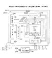
図34は本発明の半導体記憶装置の第4実施形態の要部を示す回路図であり、本発明の半導体記憶装置の第4実施形態は、図33に示す本発明の電子装置の第4実施形態が備えるDRAM178に使用することができるものである。
【0155】
図34中、183はコントローラ179からのコマンド信号をデコードするコマンドデコーダ、184はコントローラ179からのアドレス信号A0〜Anを入力するアドレス入力回路、185はリード/ライトデータDQ0〜DQnの入出力を行うデータ入出力回路である。
【0156】
また、186はコントローラ179からのコマンド信号をNOR処理するNOR回路、187はコントローラ179からのアドレス信号A0〜AnをNOR処理するNOR回路、188はNOR回路186、187の出力をNAND処理するNAND回路である。
【0157】
ここに NOR回路186の出力は、コマンド信号が全てLレベルの場合のみHレベルとなり、NOR回路187の出力は、アドレス信号A0〜Anが全てLレベルの場合のみHレベルとなるので、NAND回路188の出力は、コマンド信号及びアドレスA0〜Anが全てLレベルの場合のみLレベルとなり、この場合には、自動的にデータ待避モードとなる。
【0158】
また、189はフラッシュメモリ180からのビジー信号BUSY2を受信するためのBUSY2入力バッファ、190はデータの待避を制御するデータ待避制御回路であり、データ待避制御回路は、NAND回路188の出力がLレベルになると、すなわち、コントローラ179からのコマンド信号及びアドレス信号が全てLレベルになると、BUSY2入力バッファ189を活性化するビジーイネーブル信号BENを出力すると共に、データ待避制御信号ESCを出力し、その後、BUSY2入力バッファ189がビジー信号BUSY2を入力するごとに、データ待避制御信号ESCを出力するというものである。
【0159】
また、191はデータ待避制御信号ESCを受けて、待避させるべきデータのアドレスを出力するデータ待避アドレスカウンタ、192はデータ待避制御信号ESCを受けてリフレッシュ制御信号REFを出力するリフレッシュ制御回路、193はリフレッシュ制御信号REFをトリガ信号としてリフレッシュアドレスを出力するリフレッシュカウンタである。
【0160】
また、194−0、194−1はバンクアドレス信号により選択されるバンクであり、バンク194−0、194−1は同一回路構成とされており、バンク194−0において、195−0〜195−3は図3に示すブロック12−0〜12−3と同様に構成されたブロックである。
【0161】
また、196はブロック195−0〜195−3により共有されるデータバス、197はブロック195−0〜195−3により共有されるライトアンプ/センスバッファ、198はバンク194−0の動作を制御する制御回路である。
【0162】
また、199は制御回路198に制御されて、リード/ライト時には、アドレス入力回路184から出力されるロウアドレス信号を選択し、リフレッシュ時には、リフレッシュカウンタ193から出力されるリフレッシュアドレスを選択し、データ待避時には、データ待避アドレスカウンタ191から出力されるデータ待避アドレスを選択するセレクタである。また、200はセレクタ199から出力されるアドレス信号をラッチするアドレスラッチ回路、201はコラムアドレスカウンタである。
【0163】
図35は本発明の半導体記憶装置の第4実施形態を図33に示す電子装置のDRAM178に適用した場合の動作例を示す波形図であり、図35Aは主電池から供給される電源電圧、図35Bはコントローラから出力されるコマンド信号及びアドレス信号、図35Cはビジーイネーブル信号BEN、図35Dはデータ待避信号ESC、図35Eは出力データ、図35Fはフラッシュメモリの動作状態、図35Gはビジー信号BUSY2を示している。
【0164】
図33に示す電子装置においては、主電池からの電源電圧が途絶えると、コントローラ179から出力されるコマンド信号及びアドレス信号は全てLレベルとなり、本発明の半導体記憶装置の第4実施形態においては、NAND回路188の出力=Lレベルとなるので、ビジーイネーブル信号BENがHレベルとなり、BUSY2入力回路189が活性化されると共に、最初のデータ待避制御信号ESCが出力されてデータ待避モードに設定され、最初の待避データD0が出力され、これがフラッシュメモリ180に書き込まれ、この間、ビジー信号BUSY2=Lレベルとなり、ライト中であることが表示される。ビジー信号BUSY2=Lレベルの間、データ待避制御信号ESCは停止し、リフレッシュが再開される。
【0165】
その後、フラッシュメモリ180において待避データD0のライトが終了すると、ビジー信号BUSY2=Hレベルとなり、これがBUSY2入力回路189を介してデータ待避制御回路190に供給され、2番目のデータ待避制御信号ESCが出力され、これに対応して、2番目の待避データD1が出力され、これがフラッシュメモリ180に書き込まれ、この間、ビジー信号BUSY2=Lレベルとなり、ライト中であることが表示される。ビジー信号BUSY2=Lレベルの間、データ待避制御信号ESCは停止し、リフレッシュが再開される。
【0166】
その後、フラッシュメモリ180においてデータD1のライトが終了すると、ビジー信号BUSY2=Hレベルとなり、これがBUSY2入力回路189を介してデータ待避制御回路190に供給され、3番目のデータ待避制御信号ESCが出力され、これに対応して、3番目の待避データD1が出力され、これがフラッシュメモリ180に書き込まれ、この間、ビジー信号BUSY2=Lレベルとなり、ライト中であることが表示される。以下、待避データがなくなるまで、同様の動作が繰り返される。
【0167】
このように、本発明の半導体記憶装置の第4実施形態によれば、これを図33のDRAM178に適用した場合、主電池が切れたり、外れたりして、主電池による電源電圧の供給が途絶えた場合に、本発明の半導体記憶装置の第4実施形態が記憶するデータをリフレッシュを必要としないフラッシュメモリ180に待避させることができる。
【0168】
したがって、本発明の電子装置の第4実施形態をDRAMを搭載する携帯電話などの簡易端末に適用する場合には、主電池が切れたり、外れたりして、主電池による電源電圧の供給が途絶えた場合に、DRAM178のリフレッシュによるバックアップ用電池の消費を出来る限り少なくすることができる。
【0169】
本発明の電子装置の第5実施形態・・図36
図36は本発明の電子装置の第5実施形態の要部を示す回路図であり、本発明の電子装置の第5実施形態は、図33に示す本発明の電子装置の第4実施形態が備えるDRAM178及びフラッシュメモリ180と回路構成の異なるDRAM203及びフラッシュメモリ204を設け、その他については、図33に示す本発明の電子装置の第4実施形態と同様に構成したものである。
【0170】
ここに、DRAM203は、出力データと共に、出力データの取り込みのタイミングを指示するデータストローブ信号QSを出力するように構成されており、フラッシュメモリ204は、DRAM203からのデータストローブ信号QSを受信し、データストローブ信号QSの指示するタイミングでDRAM203からの出力データの取り込みを行うことができるように構成されている。
【0171】
このように構成された本発明の電子装置の第5実施形態によれば、図33に示す本発明の電子装置の第4実施形態と同様の効果を得ることができると共に、DRAM203からのデータの取り込み制御を容易に行うことができる。
【0172】
本発明の半導体記憶装置の第5実施形態・・図37、図38
図37は本発明の半導体記憶装置の第5実施形態の要部を示す回路図であり、本発明の半導体記憶装置の第5実施形態は、図36に示す本発明の電子装置の第5実施形態が備えるDRAM203として使用することができるものである。
【0173】
本発明の半導体記憶装置の第5実施形態は、データ待避用クロックを発生するデータ待避用クロック発生回路206及びデータストローブ信号QSを発生するQS出力回路207を設け、データ待避動作時に、データ待避用クロック発生回路206からデータ待避用クロックを発生し、データ待避アドレスカウンタ191やQS出力回路207等をデータ待避用クロックに同期させて動作させ、出力データとデータストローブ信号QSとの出力タイミングが適正となるようにし、その他については、図34に示す本発明の半導体記憶装置の第4実施形態と同様に構成したものである。
【0174】
ここに、データ待避用クロック発生回路206は、オシレータを内蔵することによりデータ待避用クロックを発生するようにしても良いし、あるいは、本発明の半導体記憶装置の第5実施形態を使用する電子装置に備えられる水晶発振器等からのクロック信号を利用してデータ待避用クロックを発生するようにしても良い。
【0175】
図38は本発明の半導体記憶装置の第5実施形態を図36に示す電子装置のDRAM203に適用した場合の動作例を示す波形図であり、図38Aは主電池から供給される電源電圧、図38Bはコントローラから出力されるコマンド信号及びアドレス信号、図38Cはビジーイネーブル信号BEN、図38Dはデータ待避信号ESC、図35Eはデータ待避用クロック発生回路206から出力されるデータ待避用クロックECK、図35Fは出力データ、図38Gはデータストローブ信号QS、図38Hはフラッシュメモリ204の動作状態、図38Iはビジー信号BUSY2を示している。
【0176】
図36に示す電子装置においては、主電池からの電源電圧が途絶えると、コントローラ179から出力されるコマンド信号及びアドレス信号は全てLレベルとなり、本発明の半導体記憶装置の第5実施形態においては、NAND回路188の出力=Lレベルとなるので、ビジーイネーブル信号BENがHレベルとなり、BUSY2入力回路189及びデータ待避用クロック発生回路206が活性化されると共に、最初のデータ待避制御信号ESCが出力されてデータ待避モードとなり、最初の待避データD0が出力され、これがフラッシュメモリ204に書き込まれ、この間、ビジー信号BUSY2=Lレベルとなり、ライト中であることが表示される。ビジー信号BUSY2=Lレベルの間、データ待避制御信号ESCは停止し、リフレッシュが再開される。
【0177】
その後、フラッシュメモリ204において待避データD0のライトが終了すると、ビジー信号BUSY2=Hレベルとなり、この結果、これがBUSY2入力回路189を介してデータ待避制御回路190に供給され、2番目のデータ待避制御信号ESCが出力され、これに対応して、2番目の待避データD1が出力されると共に、データストローブ信号QSが出力され、待避データD1がフラッシュメモリ204に書き込まれ、この間、ビジー信号BUSY2=Lレベルとなり、ライト中であることが表示される。ビジー信号BUSY2=Lレベルの間、データ待避制御信号ESCは停止し、リフレッシュが再開される。
【0178】
その後、フラッシュメモリ204においてデータD1のライトが終了すると、ビジー信号BUSY2=Hレベルとなり、この結果、これがBUSY2入力回路189を介してデータ待避制御回路190に供給され、3番目のデータ待避制御信号が出力され、これに対応して、3番目の待避データD1が出力されると共に、データストローブ信号QSが出力され、待避データD2がフラッシュメモリ204に書き込まれ、この間、ビジー信号BUSY2=Lレベルとなり、ライト中であることが表示される。以下、待避データがなくなるまで、同様の動作が繰り返される。
【0179】
本発明の半導体記憶装置の第5実施形態によれば、これを、図36に示すDRAM203に適用する場合には、図34に示す本発明の半導体記憶装置の第4実施形態と同様の効果を得ることができると共に、フラッシュメモリ204による待避データの取り込み制御を容易に行うことができる。
【0180】
本発明の電子装置の第6実施形態・・図39、図40
図39は本発明の電子装置の第6実施形態の要部を示す回路図であり、本発明の電子装置の第6実施形態は、図33に示す本発明の電子装置の第4実施形態が備えるDRAM178及びフラッシュメモリ180と回路構成の異なるDRAM209及びフラッシュメモリ210を設け、その他については、図33に示す本発明の電子装置の第4実施形態と同様に構成したものである。
【0181】
ここに、DRAM209は、ビジー信号BUSY2を入力するBUSY2入力回路211及びデータストローブ信号QSを出力するQS信号出力回路212を内蔵し、ビジー信号入力端子及びデータストローブ信号出力端子として兼用する外部端子213を設けて構成されている。
【0182】
また、フラッシュメモリ210は、ビジー信号BUSY2を出力するBUSY2出力回路214及びデータストローブ信号QSを入力するQS入力回路215を内蔵し、ビジー信号出力端子及びデータストローブ信号入力端子として兼用する外部端子216を設けて構成されている。
【0183】
図40はBUSY2入力回路211、QS出力回路212、BUSY2出力回路214及びQS入力回路215の構成例を示す回路図である。図40中、BUSY2入力回路211において、218はビジー信号BUSY2入力用のインバータ、QS出力回路212において、219はデータストローブ信号QS出力用のNMOSトランジスタである。
【0184】
また、BUSY2出力回路214において、220はビジー信号BUSY2出力用のNMOSトランジスタ、QS入力回路215において、221はデータストローブ信号QS入力用のインバータである。
【0185】
なお、この場合、QS出力回路212及びBUSY2出力回路214はオープインドレイン出力とされているので、ビジー信号BUSY2及びデータストローブ信号QSの信号レベルを確保させるために、BUSY2/QS共通線222と電源VDDとの間に高抵抗223を必要とする。
【0186】
このように構成された本発明の電子装置の第6実施形態によれば、図33に示す本発明の電子装置の第4実施形態と同様の効果を得ることができると共に、DRAM209からのデータの取り込み制御を容易に行うことができ、しかも、DRAM209及びフラッシュメモリ210の外部端子の数を減らすことができる。
【0187】
本発明の半導体記憶装置の第6実施形態・・図41〜図43
図41は本発明の半導体記憶装置の第6実施形態の要部を示す回路図であり、本発明の半導体記憶装置の第6実施形態は、図39に示す本発明の電子装置の第6実施形態が備えるDRAM209に使用することができるものである。
【0188】
本発明の半導体記憶装置の第6実施形態は、ビジー信号入力端子及びデータストローブ信号出力端子として兼用する外部端子225を設け、外部端子225とBUSY2入力回路189の入力端子226及びQS出力回路207の出力端子227とを接続し、その他については、図37に示す本発明の半導体記憶装置の第5実施形態と同様に構成したものである。
【0189】
図42は本発明の半導体記憶装置の第6実施形態を図39に示す電子装置のDRAM209に適用した場合の動作例を示す波形図であり、図42Aは主電池から供給される電源電圧、図42Bはコントローラから出力されるコマンド信号及びアドレス信号の状態、図42Cはビジーイネーブル信号BEN、図42Dはデータ待避信号ESC、図42Eは出力データ、図42FはBUSY2/QS共通線の電位、図42Gはフラッシュメモリ210の状態を示している。
【0190】
図39に示す電子装置においては、主電池からの電源電圧が途絶えると、コントローラ179から出力されるコマンド信号及びアドレス信号は全てLレベルとなり、本発明の半導体記憶装置の第6実施形態においては、NAND回路188の出力=Lレベルとなるので、ビジーイネーブル信号BENがHレベルとなり、BUSY2入力回路189が活性化され、最初のデータ待避制御信号ESCが出力され、最初の待避データD0が出力されると共に、BUSY2/QS共通線にはLレベルからなるデータストローブ信号QSが出力され、待避データD0がQSに同期してフラッシュメモリ210に取り込まれ、これがフラッシュメモリ210に書き込まれ、この間、BUSY2/QS共通線には、Lレベルからなるビジー信号BUSY2が出力され、ライト中であることが表示される。
【0191】
その後、フラッシュメモリ210における待避データD0のライトが終了すると、BUSY2/QS共通線=Hレベルとされ、この結果、これがBUSY2入力回路189を介してデータ待避制御回路190に供給され、2番目のデータ待避制御信号ESCが出力され、これに対応して、2番目の待避データD1が出力されると共に、BUSY2/QS共通線にはLレベルからなるデータストローブ信号QSが出力され、待避データがQSに同期してフラッシュメモリ210に取り込まれ、これがフラッシュメモリ210に書き込まれ、この間、BUSY2/QS共通線には、Lレベルからなるビジー信号BUSY2が出力され、ライト中であることが表示される。
【0192】
その後、フラッシュメモリ210における待避データD1のライトが終了すると、BUSY2/QS共通線=Hレベルとされ、この結果、これがBUSY2入力回路189を介してデータ待避制御回路190に供給され、3番目のデータ待避制御信号ESCが出力され、これに対応して、2番目の待避データD2が出力されると共に、BUSY2/QS共通線にはLレベルからなるデータストローブ信号QSが出力され、待避データD2がデータストローブ信号QSに同期してフラッシュメモリ210に取り込まれ、これがフラッシュメモリ210に書き込まれ、この間、BUSY2/QS共通線には、Lレベルからなるビジー信号BUSY2が出力され、ライト中であることが表示される。
【0193】
このように、本発明の半導体記憶装置の第6実施形態によれば、これを図39に示すDRAM209に適用する場合には、図37に示す本発明の半導体記憶装置の第5実施形態と同様の効果を得ることができると共に、外部端子の数を減らすことができる。なお、図43に示すように、複数バイトの待避データをバーストモードで連続してまとめて出力するようにしても良い。
【0194】
本発明の半導体記憶装置の第7実施形態・・図44
図44は本発明の半導体記憶装置の第7実施形態の要部を示す回路図であり、本発明の半導体記憶装置の第7実施形態は、図36に示すDRAM203に使用することができるものである。
【0195】
本発明の半導体記憶装置の第7実施形態は、データ待避アドレスカウンタ191から出力されるデータ待避アドレスと、リフレッシュカウンタ193から出力されるリフレッシュアドレスとを比較する比較器229と、この比較器229の出力N2をゲート信号として、リフレッシュ制御回路192から出力されるリフレッシュ制御信号REFの伝送を制御するAND回路230とを設け、その他については、図37に示す本発明の半導体記憶装置の第5実施形態と同様に構成したものである。
【0196】
比較器229は、データ待避制御回路190から出力される制御信号N1に制御されるものであり、制御信号N1=Hレベルの場合に比較動作を行うものであるが、制御信号N1は、データ待避モード時にはHレベル、その他の場合には、Lレベルとされ、比較器229の出力N2は、リフレッシュアドレスがデータ待避アドレスよりも大きい場合のみHレベルとなり、その他の場合には、Lレベルを維持するようにされている。
【0197】
ここに、データ待避時に、比較器229の出力=Hレベルの場合、すなわち、出力されたリフレッシュアドレスが出力されたデータ待避アドレスよりも大きく、出力されたリフレッシュアドレスのデータが待避されていない場合には、リフレッシュ制御信号REFが出力されることになるので、出力されたリフレッシュアドレスについてリフレッシュが行われることになる。
【0198】
これに対して、比較器229の出力=Lレベルの場合、すなわち、出力されたリフレッシュアドレスが出力されたデータ待避アドレスよりも小さく、出力されたリフレッシュアドレスのデータが既に待避されている場合には、リフレッシュ制御信号REFがAND回路230から出力されることはないので、出力されたリフレッシュアドレスについてリフレッシュが行われることはない。
【0199】
このように、本発明の半導体記憶装置の第7実施形態によれば、図37に示す本発明の半導体記憶装置の第5実施形態と同様の効果を得ることができると共に、既に待避させたデータのアドレスについては、リフレッシュされることがないので、バックアップ用の電池の消費を図37に示す本発明の半導体記憶装置の第5実施形態の場合よりも少なくすることができる。
【0200】
本発明の半導体記憶装置の第8実施形態・・図45
図45は本発明の半導体記憶装置の第8実施形態の要部を示す回路図であり、本発明の半導体記憶装置の第8実施形態は、図34に示す本発明の半導体記憶装置の第4実施形態が備えるバンク194−0、194−1と回路構成の異なるバンク232−0、232−1を設け、その他については、図34に示す本発明の半導体記憶装置の第4実施形態と同様に構成したものである。
【0201】
ここに、バンク232−0、232−1は、同一回路構成とされており、バンク232−0において、233−0〜233−3はブロックである。ブロック233−0〜233−3は同一回路構成とされており、ブロック233−0において、234はメモリセルアレイ、235はロウデコーダ、236はセンスアンプ、237はコラムデコーダ、238はデータ待避動作時、制御回路239に接続されて、メモリセルアレイ234からリードしたデータを後述するシリアルレジスタに転送するための転送ゲートである。
【0202】
また、240はブロック233−0〜233−3により共有されるシリアルレジスタ、241はブロック233−0〜233により共有されるライトアンプ/センスバッファであり、センスバッファは、データ待避時は、シリアルレジスタ240から出力されるデータをデータ入出力回路185に供給するように動作する。バンク232−0、232−1のその他の部分については、図34に示すバンク194−0、194−1と同様に構成されている。
【0203】
すなわち、本発明の半導体記憶装置の第8実施形態は、待避データを行ごとに、シリアルレジスタ240に格納し、このシリアルレジスタ240に格納された待避データをセンスバッファ及びデータ入出力回路185を介して出力させるというものである。
【0204】
このように構成された本発明の半導体記憶装置の第8実施形態によれば、待避データの出力中にリフレッシュ動作を行うことができるので、動作の効率化を図ることができる。
【0205】
ここで、本発明の半導体記憶装置及び電子装置を整理すると、本発明の半導体記憶装置及び電子装置には、以下のような半導体記憶装置及び電子装置が含まれる。
【0206】
(1) データ保持にリフレッシュを必要とする半導体記憶装置であって、リフレッシュ期間中、外部にビジー信号を出力するように構成されていることを特徴とする半導体記憶装置。
【0207】
(2) 前記(1)に記載の半導体記憶装置において、リフレッシュ時期が到来したことを検出し、リフレッシュを自己管理するリフレッシュ制御回路を備えていることを特徴とする半導体記憶装置。
【0208】
(3) 前記(2)に記載の半導体記憶装置において、タイマー回路を内蔵し、前記リフレッシュ制御回路は、前記タイマー回路の出力に基づいてリフレッシュ時期が到来したことを検出することを特徴とする半導体記憶装置。
【0209】
(4) 前記(2)に記載の半導体記憶装置において、前記リフレッシュ制御回路は、外部から供給されるクロック信号に基づいてリフレッシュ時期が到来したことを検出することを特徴とする半導体記憶装置。
【0210】
(5) 前記(2)、(3)又は(4)に記載の半導体記憶装置において、前記ビジー信号を発生するビジー信号発生回路と、外部から供給されるコマンド信号をデコードするコマンドデコーダとを備え、前記リフレッシュ制御回路は、リフレッシュ時期が到来したことを示すリフレッシュ制御信号を発生し、前記コマンドデコーダで処理を開始した又は処理中のコマンドがない場合は、リフレッシュ制御信号に応じてリフレッシュを開始させ、前記コマンドデコーダで処理を開始した又は処理中のコマンドがある場合は、その処理を待ってリフレッシュを開始させ、前記ビジー信号発生回路は、リフレッシュ制御信号に応答してビジー信号を発生し、リフレッシュが終了したら、前記ビジー信号を解除することを特徴とする半導体記憶装置。
【0211】
(6) 前記(5)に記載の半導体記憶装置において、前記ビジー信号を発生している間は、外部からのコマンド信号及びアドレス信号を取り込まないことを特徴とする半導体記憶装置。
【0212】
(7) 前記(5)に記載の半導体記憶装置において、前記ビジー信号の発生中に外部から供給されたコマンド信号を一時保管するレジスタを備え、リフレッシュ終了後に前記レジスタに保管されたコマンドを優先的に処理することを特徴とする半導体記憶装置。
【0213】
(8) 前記(1)〜(7)のいずれかに記載の半導体記憶装置と、この半導体記憶装置を制御するコントローラとを備え、前記コントローラは、前記半導体記憶装置からビジー信号が出力されている間は、前記半導体記憶装置にアクセスしないことを特徴とする電子装置。
【0214】
(9) 前記(1)〜(7)のいずれかに記載の半導体記憶装置と、この半導体記憶装置を制御するコントローラとを備え、前記コントローラは、半導体記憶装置からビジー信号が出力されている間は、同一のコマンドを繰り返し出力することを特徴とする電子装置。
【0215】
(10) 前記(1)〜(4)のいずれかに記載の半導体記憶装置と、この半導体記憶装置を制御するコントローラとを備え、前記コントローラは、半導体記憶装置のリフレッシュカウンタに対応するカウンタを備え、前記半導体記憶装置からビジー信号が出力されたときは、カウンタを動作させることを特徴とする電子装置。
【0216】
(11) 或るワード線により選択されているメモリセルのリフレッシュ中に、前記或るワード線を含むメモリブロックに対するコマンドを受け付け、前記或るワード線により選択されているメモリセルのリフレッシュを中断してコマンドを実行し、前記或るワード線により選択されるメモリセルのリフレッシュを再開することを特徴とする半導体記憶装置。
【0217】
(12) 前記(11)に記載の半導体記憶装置において、リフレッシュ中のメモリセルのデータを待避させるデータ待避用レジスタと、前記データ待避用レジスタにデータを転送する転送ゲートとを備え、コマンドの実行は、前記転送ゲートにより前記データ待避用レジスタにリフレッシュ中のメモリセルのデータを転送してから行い、リフレッシュ再開時、前記データ待避用レジスタからデータを返送することを特徴とする半導体記憶装置。
【0218】
(13) 前記(12)に記載の半導体記憶装置において、再開したリフレッシュ実行中に第2のコマンドを受け付け、再開したリフレッシュを中断して第2のコマンドを実行し、リフレッシュを再開することを特徴とする半導体記憶装置。
【0219】
(14) 前記(12)又は(13)に記載の半導体記憶装置において、前記転送ゲートは、センスアンプで増幅中のビット線上のデータを前記データ待避用レジスタに転送することを特徴とする半導体記憶装置。
【0220】
(15) 前記(12)又は(13)に記載の半導体記憶装置において、前記転送ゲートは、センスアンプで増幅していないビット線上のデータを前記データ待避用レジスタに転送することを特徴とする半導体記憶装置。
【0221】
(16) 前記(12)に記載の半導体記憶装置において、リフレッシュ中のアドレスとコマンドを実行するためのロウアドレスとを比較する比較器を備え、リフレッシュ中のアドレスとコマンドを実行するためのロウアドレスとが一致していない場合は、リフレッシュを中断してコマンドを実行し、リフレッシュ中のアドレスと前記コマンドを実行するためのロウアドレスとが一致している場合は、リフレッシュを終了し、ビット線のプリチャージを行わないで前記コマンドを実行することを特徴とする半導体記憶装置。
【0222】
(17) 前記(16)に記載の半導体記憶装置において、リフレッシュ中のアドレスと前記コマンドを実行するためのロウアドレスとが一致していないことによりリフレッシュを中断した場合には、リフレッシュ開始からリフレッシュ中断までの長さにより、リフレッシュ中断に続くプリチャージ期間の長さを調整することを特徴とする半導体記憶装置。
【0223】
(18) 外部から自動読出しを指示されたときは、自動読出しのためのアドレス信号を発生するアドレスカウンタと、自動読出しするデータの転送先が出力するアクセスの受け付けを許可するか否かを示すアクセス受け付け許否信号を受信するアクセス受け付け許否信号受信手段とを含み、外部から自動読出しを指示され、かつ、前記アクセス受け付け許否信号がアクセスの受け付けを許可しているときは、データを自動的に読出す自動読出し手段を備えていることを特徴とする半導体記憶装置。
(19) 前記(18)に記載の半導体記憶装置において、通常動作モードにおいては、外部から入力されたアドレス信号に基づく第1のアドレスを選択してデコーダに伝達し、自動読み出しモードにおいては、前記自動読み出しアドレスカウンタで発生した第2のアドレスを選択しデコーダに伝達するセレクタを備えていることを特徴とする半導体記憶装置。
【0224】
(20) 前記(19)に記載の半導体記憶装置において、データ保持にリフレッシュを必要とするメモリセルが配列されたメモリ領域と、リフレッシュアドレスを発生するリフレッシュカウンタを備え、前記セレクタは、通常動作モードにおいては、第1のアドレスとリフレッシュアドレスを切り替え、前記自動読み出しモードにおいては、前記第2のアドレスと前記リフレッシュアドレスを切り替えることを特徴とする半導体記憶装置。
【0225】
(21) 前記(20)に記載の半導体記憶装置において、前記アクセス受け付け許否信号がアクセスの受け付けを許可していない間にリフレッシュを行うことを特徴とする半導体記憶装置。
【0226】
(22) 前記(18)に記載の半導体記憶装置において、データストローブ信号発生回路を備え、前記自動読み出しモードにおいては、データと共にデータストローブ信号を出力することを特徴とする半導体記憶装置。
【0227】
(23) 前記(22)に記載の半導体記憶装置において、データストローブ信号に同期して連続した所定の複数個のデータを出力することを特徴とする半導体記憶装置。
【0228】
(24) 前記(23)に記載の半導体記憶装置において、クロック信号を発生するクロック発生回路を備え、前記クロック信号に基づいてデータとデータストローブとを出力することを特徴とする半導体記憶装置。
【0229】
(25) 前記(24)に記載の半導体記憶装置において、オシレータを内蔵し、前記クロック発生回路は、前記オシレータの出力に基づいてクロック信号を発生することを特徴とする半導体記憶装置。
【0230】
(26) 前記(24)に記載の半導体記憶装置において、前記クロック発生回路は、外部から供給される外部クロック信号に基づいてクロック信号を発生することを特徴とする半導体記憶装置。
【0231】
(27) 前記(22)又は(23)に記載の半導体記憶装置において、前記データストローブ信号と前記データ受け付け許否信号信号は、共通の端子から入出力されることを特徴とする半導体記憶装置。
【0232】
(28) 前記(20)に記載の半導体記憶装置において、前記第2のアドレス信号と前記リフレッシュアドレス信号を比較する比較器を備え、前記比較器の比較結果に基づきリフレッシュを実施することを特徴とする半導体記憶装置。
【0233】
(29) 前記(23)に記載の半導体記憶装置において、複数のデータを取り込みシリアルに出力するシリアルレジスタと、メモリセルの一部のデータを前記シリアルレジスタに転送する転送ゲートとを備え、前記自動読み出しモードにおいては、前記シリアルレジスタにデータを転送し、前記シリアルレジスタを介して出力することを特徴とする半導体記憶装置。
【0234】
(30) 外部から自動書込みを指示されたときは、書込みデータを内部で発生するアドレスに自動的に書込む自動書込み手段と、自動書込み動作中は、自動書込み動作中であることを明示する自動書込み動作中明示信号を外部に出力する自動書込み中明示信号出力手段とを備えていることを特徴とする半導体記憶装置。
【0235】
(31) 前記(30)に記載の半導体記憶装置において、データストローブ信号入力回路を備え、前記自動書込みモードにおいて、データストローブ信号に同期して書込みデータを取り込むことを特徴とする半導体記憶装置。
【0236】
(32) 前記(18)〜(29)のいずれかに記載の半導体記憶装置と、前記(30)又は(31)に記載の半導体記憶装置とを備える電子装置。
【0237】
【発明の効果】
以上のように、本発明中、第1の発明によれば、データ保持にリフレッシュを必要とする半導体記憶装置に関し、リフレッシュ期間中、外部にビジー信号を出力するように構成するとしたことにより、データ保持にリフレッシュを必要とする半導体記憶装置と、この半導体記憶装置を制御するコントローラとを搭載する電子装置における半導体記憶装置に第1の発明の半導体記憶装置を使用する場合には、コントローラは、半導体記憶装置がリフレッシュ期間中であるか否かを知ることができるので、コントローラによる半導体記憶装置の制御の容易化を図ることができる。
【0238】
第2の発明によれば、データ保持にリフレッシュを必要とする半導体記憶装置と、この半導体記憶装置を制御するコントローラとを搭載する電子装置に関し、半導体記憶装置は、リフレッシュ期間中、外部にビジー信号を出力するように構成し、コントローラは、ビジー信号を受信することができるように構成するとしたことにより、コントローラは、半導体記憶装置がリフレッシュ期間中であるか否かを知ることができるので、コントローラによる半導体記憶装置の制御の容易化を図ることができる。
【0239】
また、第3の発明によれば、半導体記憶装置に関し、外部から自動書込みを指示されたときは、書込みデータを内部で発生するアドレスに自動的に書込む自動書込み手段を備えるとしたので、たとえば、第1の半導体記憶装置と、第1の半導体記憶装置を制御するコントローラとを備える電子装置において、第1の半導体記憶装置のデータを待避させるための第2の半導体記憶装置を設けようとする場合、第2の発明を第2の半導体記憶装置として使用する場合には、第1の半導体記憶装置のデータの待避を容易に行うことができる。
【0240】
また、第4の発明によれば、外部から自動読出しを指示され、かつ、データの転送先が出力するアクセス受け付け許否信号がデータの受け付けを許可しているときは、データを自動的に読出す自動読出し手段を備えているので、データ転送の必要がある場合(たとえば、データ待避の必要がある場合)に、データ受け付け許否信号を出力するデータ転送先(データ待避先)にデータを容易に転送(待避)させることができる。
【図面の簡単な説明】
【図1】本発明の電子装置の第1実施形態の要部を示す回路図である。
【図2】本発明の電子装置の第1実施形態が備えるDRAM及びコントローラの動作例を示すタイムチャートである。
【図3】本発明の半導体記憶装置の第1実施形態の要部を示す回路図である。
【図4】本発明の半導体記憶装置の第1実施形態が備えるリフレッシュ制御回路、BUSY1出力回路及びリフレッシュカウンタの構成を示す回路図である。
【図5】本発明の半導体記憶装置の第1実施形態が備えるリフレッシュ制御回路が備えるRefz発生回路の構成を示す回路図である。
【図6】本発明の半導体記憶装置の第1実施形態が備えるリフレッシュ制御回路、BUSY1出力回路及びリフレッシュカウンタの第1動作例を示す波形図である。
【図7】本発明の半導体記憶装置の第1実施形態が備えるリフレッシュ制御回路、BUSY1出力回路及びリフレッシュカウンタの第2動作例を示す波形図である。
【図8】本発明の半導体記憶装置の第1実施形態が備えるコマンドデコーダの構成を示す回路図である。
【図9】本発明の半導体記憶装置の第1実施形態が備えるアドレス入力回路の構成を示す回路図である。
【図10】本発明の電子装置の第1実施形態が備えるコントローラの動作例を示す波形図である。
【図11】本発明の半導体記憶装置の第2実施形態の要部を示す回路図である。
【図12】本発明の半導体記憶装置の第2実施形態が備えるコマンドデコーダの構成を示す回路図である。
【図13】本発明の半導体記憶装置の第2実施形態が備えるアドレス入力回路の構成を示す回路図である。
【図14】本発明の半導体記憶装置の第2実施形態の動作を示す波形図である。
【図15】本発明の電子装置の第2実施形態の要部を示す回路図である。
【図16】本発明の電子装置の第3実施形態の要部を示す回路図である。
【図17】本発明の半導体記憶装置の第3実施形態の要部を示す回路図である。
【図18】本発明の半導体記憶装置の第3実施形態が備えるデータレジスタ及び転送ゲートの構成を示す回路図である。
【図19】本発明の半導体記憶装置の第3実施形態の第1動作例を従来のDRAMの場合との比較で示す波形図である。
【図20】本発明の半導体記憶装置の第3実施形態の第2動作例を従来のDRAMの場合との比較で示す波形図である。
【図21】本発明の半導体記憶装置の第3実施形態の第3動作例を示すタイムチャートである。
【図22】本発明の半導体記憶装置の第3実施形態の第4動作例を示す波形図である。
【図23】本発明の半導体記憶装置の第3実施形態の第5動作例及び第6動作例を示すタイムチャート
【図24】本発明の半導体記憶装置の第3実施形態の第7動作例を説明するための波形図である。
【図25】本発明の半導体記憶装置の第3実施形態の第7動作例を説明するための波形図である。
【図26】本発明の半導体記憶装置の第3実施形態が備えるプリチャージ信号発生回路の構成を示す回路図である。
【図27】本発明の半導体記憶装置の第3実施形態が備えるプリチャージ信号発生回路が備えるプリチャージ期間制御回路の構成を示す回路図である。
【図28】本発明の半導体記憶装置の第3実施形態が備えるプリチャージ信号発生回路が備える遅延時間制御回路の構成を示す回路図である。
【図29】本発明の半導体記憶装置の第3実施形態が備えるプリチャージ信号発生回路が備えるリセット信号発生回路の構成を示す回路図である。
【図30】本発明の半導体記憶装置の第3実施形態が備えるプリチャージ信号発生回路が備えるリフレッシュ時間測定信号発生回路の構成を示す回路図である。
【図31】本発明の半導体記憶装置の第3実施形態が備える遅延時間制御回路の動作を示す波形図である。
【図32】本発明の半導体記憶装置の第3実施形態の動作例を示す波形図である。
【図33】本発明の電子装置の第4実施形態の要部を示す回路図である。
【図34】本発明の半導体記憶装置の第4実施形態の要部を示す回路図である。
【図35】本発明の半導体記憶装置の第4実施形態を図33に示す電子装置のDRAMに適用した場合の動作例を示す波形図である。
【図36】本発明の電子装置の第5実施形態の要部を示す回路図である。
【図37】本発明の半導体記憶装置の第5実施形態の要部を示す回路図である。
【図38】本発明の半導体記憶装置の第5実施形態を図36に示す電子装置のDRAMに適用した場合の動作例を示す波形図である。
【図39】本発明の電子装置の第6実施形態の要部を示す回路図である。
【図40】本発明の電子装置の第6実施形態が備えるDRAMのBUSY2入力回路、QS出力回路及びフラッシュメモリのBUSY2出力回路、QS入力回路の構成例を示す回路図である。
【図41】本発明の半導体記憶装置の第6実施形態の要部を示す回路図である。
【図42】本発明の半導体記憶装置の第6実施形態を図39に示す電子装置のDRAMに適用した場合の動作例を示す波形図である。
【図43】本発明の半導体記憶装置の第6実施形態を図39に示す電子装置のDRAMに適用した場合の他の動作例を示す波形図である。
【図44】本発明の半導体記憶装置の第7実施形態の要部を示す回路図である。
【図45】本発明の半導体記憶装置の第8実施形態の要部を示す回路図である。
【符号の説明】
BUSY1 ビシー信号
BUSY2 ビシー信号
QS データストローブ信号[0001]
BACKGROUND OF THE INVENTION
The present invention relates to a semiconductor memory device that requires refresh for data retention, such as a DRAM (dynamic random access memory), an electronic device using such a semiconductor memory device, and such an electronic device. For example, the present invention relates to a semiconductor memory device suitable for use as a semiconductor memory device for data saving.
[0002]
[Prior art]
For example, DRAMs have been used for main memories of personal computers and servers until now, but in recent years, large-capacity DRAMs have been installed in simple terminals such as mobile phones due to the development of the Internet and the advancement of mobile technologies. It is becoming an era.
[0003]
[Problems to be solved by the invention]
Currently, simple terminals such as mobile phones are equipped with SRAM (static random access memory). However, when DRAM is to be installed instead of SRAM or together with SRAM, DRAM is different from SRAM in that it retains data. You must consider that a refresh is necessary.
[0004]
From this, firstly, the DRAM mounted on a simple terminal such as a mobile phone is easy to control by the controller, and secondly, the main battery of a simple terminal such as a mobile phone equipped with a DRAM has a main battery. When the supply of the power supply voltage by the main battery is cut off due to being cut or disconnected, it is required that the consumption of the backup battery by refreshing the DRAM can be reduced as much as possible.
[0005]
In view of this point, the present invention has as its first object to provide a semiconductor memory device that requires refresh for data retention and that is easily controlled by a controller. A second object of the present invention is to provide an electronic device including a required semiconductor memory device and a controller, which facilitates control of the semiconductor memory device by the controller, and data from other semiconductor memory devices. A third object is to provide a semiconductor memory device that can be easily saved, and a fourth object is to provide a semiconductor memory device that can easily save data.
[0006]
[Means for Solving the Problems]
In the present invention, the first invention is a semiconductor memory device that requires refresh for data retention, and is configured to output a busy signal to the outside during the refresh period.
[0007]
When the semiconductor memory device of the first invention is applied to a semiconductor memory device in an electronic device comprising a semiconductor memory device that requires refresh for data retention and a controller that controls the semiconductor memory device, the controller is a semiconductor Since it is possible to know whether or not the memory device is in the refresh period, it is possible to facilitate the control of the semiconductor memory device by the controller.
[0008]
In the present invention, the second invention is an electronic device comprising a semiconductor memory device that requires refresh for data retention and a controller that controls the semiconductor memory device. The controller is configured to output a busy signal, and the controller is configured to receive the busy signal.
[0009]
According to the second invention, since the controller can know whether or not the semiconductor memory device is in the refresh period, the controller controls the semiconductor memory device that requires refresh for data retention and the semiconductor memory device. With respect to an electronic device including a controller, control of the semiconductor memory device by the controller can be facilitated.
[0010]
In the present invention, the third invention is a semiconductor memory device, and when automatic writing is instructed from the outside, automatic writing means for automatically writing write data to an address generated internally, and automatic writing operation The system includes an automatic writing explicit signal output means for outputting an automatic signal during an automatic writing operation that clearly indicates that an automatic writing operation is being performed.
[0011]
According to the third aspect of the invention, the automatic semiconductor memory device is provided with the automatic writing means for automatically writing the write data to the internally generated address when the external write is instructed. For example, the first semiconductor memory device And a second semiconductor memory device for saving data stored in the first semiconductor memory device in an electronic device including the controller for controlling the first semiconductor memory device. When the second invention is used as the second semiconductor memory device, the data of the first semiconductor memory device can be easily saved.
[0012]
According to the fourth aspect of the present invention, when automatic reading is instructed from the outside, an address counter that generates an address signal for automatic reading and acceptance of an access output by a transfer destination of data to be automatically read are permitted. Including an access acceptance permission / rejection signal receiving means for receiving an access acceptance permission / rejection signal indicating whether or not to perform an automatic read from the outside, and when the access acceptance permission / permission signal permits access acceptance, An automatic reading means for automatically reading data is provided.
[0013]
According to the fourth invention, when automatic reading is instructed from the outside and the access acceptance permission / prohibition signal output from the data transfer destination permits the acceptance of the access, the automatic reading that automatically reads the data is performed. Since there is a means, when data transfer is necessary (for example, when data saving is necessary), data is easily transferred to a data transfer destination (data saving destination) that outputs an access acceptance permission / refusal signal (data saving destination). Can be saved).
[0014]
DETAILED DESCRIPTION OF THE INVENTION
The first to eighth embodiments of the semiconductor memory device of the present invention and the first to sixth embodiments of the electronic device of the present invention will be described below with reference to FIGS.
[0015]
First Embodiment of Electronic Device of the Present Invention. FIG. 1 and FIG.
FIG. 1 is a circuit diagram showing a main part of a first embodiment of an electronic device according to the present invention. In FIG. 1, 1 is a DRAM, 2 is a controller for controlling the
[0016]
Here, the
[0017]
The
[0018]
In this specification, the busy signal BUSY1 being output means that the busy signal BUSY1 is set to the L level, and the busy signal BUSYY1 being released means that the busy signal BUSY1 is set to the H level. Say.
[0019]
2 is a time chart showing an operation example of the
[0020]
That is, in this example, when the
[0021]
In this case, since the
[0022]
On the other hand, when the
[0023]
As described above, according to the first embodiment of the electronic device of the present invention, the
[0024]
Further, the
[0025]
Therefore, even if the first embodiment of the electronic device of the present invention is applied to a simple terminal such as a mobile phone and a DRAM requiring refresh is mounted on the simple terminal such as a mobile phone, the control of the DRAM by the controller is possible. It can be done easily.
[0026]
First Embodiment of Semiconductor Memory Device of the Present Invention. FIGS. 3 to 10
FIG. 3 is a circuit diagram showing the main part of the first embodiment of the semiconductor memory device of the present invention. The first embodiment of the semiconductor memory device of the present invention can be used for the
[0027]
In FIG. 3, 5 is a command decoder for inputting and decoding command signals from the controller, 6 is an address input circuit for inputting and latching address signals A0 to An from the controller, and 7 is write data / read data DQ0 to DQn. This is a data input / output circuit for inputting / outputting.
[0028]
[0029]
Reference numerals 11-0 and 11-1 denote memory areas called banks (BANK) selected by the bank address signal. The banks 11-0 and 11-1 have the same circuit configuration. , 12-0 to 12-3 are memory areas called blocks.
[0030]
The blocks 12-0 to 12-3 have the same circuit configuration. In the block 12-0, reference numeral 13 denotes a memory cell array in which memory cells are arranged, and reference numeral 14 decodes a row address signal to select a word line. A row decoder, 15 is a sense amplifier for amplifying read data from the
[0031]
Reference numeral 17 denotes a data bus shared by the blocks 12-0 to 12-3, 18 denotes a write amplifier / sense buffer shared by the blocks 12-0 to 12-3, and 19 controls the operation of the bank 11-0. It is a control circuit.
[0032]
[0033]
4 is a circuit diagram showing the configuration of the
[0034]
In the
[0035]
Reference numeral 25 indicates that when the output of the busy signal BUSY1 and the output of the command from the controller are simultaneously performed, the operation start of the
[0036]
A
[0037]
[0038]
In the
[0039]
In the
[0040]
FIG. 5 is a circuit diagram showing the configuration of the Refz generating circuit 25. In FIG. 5, 36 and 37 are NAND circuits constituting a flip-flop circuit, and 38 is an inverting delay circuit for inverting and delaying the output of the
[0041]
6 is a waveform diagram showing a first operation example of the
[0042]
FIG. 6 shows a case where the refresh control signal Ref1 is output from the
[0043]
In this case, first, the reset RS flip-
[0044]
In this case, the internal command signal Com = L level, the output S26 of the
[0045]
As a result, the refresh control signal Ref1 output from the
[0046]
That is, when the refresh control signal Ref1 is output from the
[0047]
Thereafter, when all the refresh addresses are output and all the outputs of the
[0048]
7 is a waveform diagram illustrating a second operation example of the
[0049]
FIG. 7 shows a case where the command input from the controller and the output of the refresh control signal Ref1 are simultaneous. Specifically, in the case where the commands C1, C2, and C3 are scheduled to be continuously output from the controller, the case where the input of the command C1 and the output of the refresh control signal Ref1 are simultaneous is shown.
[0050]
In this case, first, the reset RS flip-
[0051]
In this case, the internal command signal Com = H level, the output of the
[0052]
After that, when the refresh control signal Ref1 becomes L level, the output S26 of the
[0053]
Further, by setting the internal command signal Com = H level and the output S26 = L level of the
[0054]
Further, when the internal command signal Com = H level, the ras system activation signal RASz = H level, but when the execution of the command C1 ends, the las system activation signal RASz = L level, and as a result, Refz. In the generation circuit 25, the output of the
[0055]
Therefore, when the input of the command C1 and the output of the refresh control signal Ref1 are simultaneous, the busy signal BUSY1 is set to the L level, but after the execution of the command C1 is completed, the refresh address is output from the
[0056]
After that, when all the refresh addresses are output and all the outputs of the
[0057]
As described above, in the first embodiment of the semiconductor memory device of the present invention, when the command input from the controller and the output of the refresh control signal Ref1 are simultaneous, the command execution is prioritized and the command execution is performed. After that, refresh is performed.
[0058]
FIG. 8 is a circuit diagram showing the configuration of the
[0059]
46-0 and 46-m are part of a transmission gate that controls transmission of a command output from the
[0060]
The transmission gates 46-0 to 46-m are turned on when the busy signal BUSY1 = H level, and are turned off when the busy signal BUSY1 = L level. Assuming that a command is output, no command signal is captured.
[0061]
A
[0062]
FIG. 9 is a circuit diagram showing the configuration of the address input circuit 6. In FIG. 9, 51 is an input buffer for buffering the address signals A0 to An from the controller, and 52 is an inverter for inverting the busy signal BUSY1.
[0063]
Reference numerals 53-0 and 53-n are part of transmission gates for controlling transmission of the address signals A0 to An output from the
[0064]
The transmission gates 53-0 to 53-n are turned on when the busy signal BUSY1 = H level, and are turned off when the busy signal BUSY1 = L level. Even if the address signals A0 to An are output, the address signals A0 to An are not taken in. An
[0065]
As described above, according to the first embodiment of the semiconductor memory device of the present invention, refresh is self-managed by the
[0066]
Further, according to the first embodiment of the semiconductor memory device of the present invention, the busy signal BUSY1 is output from the
[0067]
Furthermore, according to the first embodiment of the semiconductor memory device of the present invention, when the command input and the output of the busy signal BUSY1 are simultaneous, the controller is configured to give priority to the execution of the command. Even when the command is input and the busy signal BUSY1 is output at the same time, it is not necessary to output the command again. From this point, the access control by the controller is facilitated.
[0068]
According to the first embodiment of the semiconductor memory device of the present invention, while the busy signal BUSY1 is being output, the
[0069]
Second Embodiment of Semiconductor Memory Device of the Present Invention. FIG. 11 to FIG.
FIG. 11 is a circuit diagram showing the main part of the second embodiment of the semiconductor memory device of the present invention. The second embodiment of the semiconductor memory device of the present invention can be used for the
[0070]
The second embodiment of the semiconductor memory device of the present invention is provided with a
[0071]
The
[0072]
The
[0073]
FIG. 12 is a circuit diagram showing a configuration of the
[0074]
[0075]
[0076]
FIG. 13 is a circuit diagram showing the configuration of the
[0077]
[0078]
[0079]
FIG. 14 is a waveform diagram showing the operation of the second embodiment of the semiconductor memory device of the present invention, FIG. 14A is a command output from the controller, FIG. 14B is a refresh control signal Ref1, FIG. 14C is a busy signal BUSY1, and FIG. Is the busy signal BUSY1a, FIG. 14E is the busy signal BUSY1b, FIG. 14F is the output of the
[0080]
In FIG. 14, after the command C1 is output from the controller, the refresh control signal Ref1 is output from the
[0081]
In this case, the command C1 is transmitted and decoded in the
[0082]
Further, as shown in FIG. 14B, the refresh control signal Ref1 is output from the
[0083]
On the other hand, in response to the busy signal BUSY1 changing to the L level, the busy signal BUSY1a changes from the H level to the L level, and the command C2 output from the controller is input to the
[0084]
When the refresh is completed and the busy signal BUSY1 changes from the L level to the H level (when the busy signal BUSY1 is released), the busy signal BUSY1b changes from the H level to the L level, and the command decoder The command C2 temporarily stored in the 60
[0085]
According to the second embodiment of the semiconductor memory device of the present invention, refresh is self-managed by the
[0086]
Further, according to the second embodiment of the semiconductor memory device of the present invention, the busy signal BUSY1 is output from the
[0087]
Second Embodiment of Electronic Device of the Invention FIG. 15
FIG. 15 is a circuit diagram showing the main part of the second embodiment of the electronic device of the present invention. The second embodiment of the electronic device of the present invention is the same as the first embodiment of the electronic device of the present invention shown in FIG. A
[0088]
The
[0089]
Therefore, when using, for example, the first embodiment of the semiconductor memory device of the present invention shown in FIG. 3 or the second embodiment of the semiconductor memory device of the present invention shown in FIG. 11 as the
[0090]
According to the second embodiment of the electronic device of the present invention configured as described above, the same effects as those of the first embodiment of the electronic device of the present invention shown in FIG. Since it is possible to access banks in the
[0091]
Third Embodiment of Electronic Device of the Present Invention. FIG.
FIG. 16 is a circuit diagram showing a main part of a third embodiment of the electronic device of the present invention. In FIG. 16, 78 is a DRAM, 79 is a controller for controlling the
[0092]
The
[0093]
According to the third embodiment of the electronic device of the present invention, the
[0094]
The
[0095]
Therefore, even if the third embodiment of the electronic device of the present invention is applied to a simple terminal such as a mobile phone and a DRAM requiring refresh is mounted on the simple terminal such as a mobile phone, the DRAM is controlled by the controller. It can be done easily.
[0096]
Third Embodiment of Semiconductor Memory Device of the Present Invention. FIG. 17 to FIG.
FIG. 17 is a circuit diagram showing the main part of the third embodiment of the semiconductor memory device of the present invention. The third embodiment of the semiconductor memory device of the present invention can be used for the
[0097]
In FIG. 17, 82 is a command decoder for decoding a command signal from the controller, 83 is an address input circuit for inputting address signals A0 to An from the controller, and 84 is data for inputting / outputting write data / read data DQ0 to DQn. It is an input / output circuit.
[0098]
85 is a refresh control circuit that self-manages refresh and periodically outputs the refresh control signal REF, 86 is a refresh counter that outputs a refresh address using the refresh control signal REF as a trigger signal, and 87 is output from the
[0099]
Reference numerals 88-0 and 88-1 are banks selected by a bank address signal. The banks 88-0 and 88-1 have the same circuit configuration. In the bank 88-0, 89-0 to 89- 3 is a block. The blocks 89-0 to 89-3 have the same circuit configuration. In the block 89-0, 90 is a memory cell array, 91 is a row decoder, 92 is a sense amplifier, and 93 is a column decoder.
[0100]
Further, 94 is a data register for temporarily storing data being read to the bit line at the time of refresh, 95 is a transfer gate for connecting the bit line and the data register, and 96 is for controlling ON / OFF of the transfer gate. It is a transfer gate signal generation circuit for generating a transfer gate signal.
[0101]
Reference numeral 97 denotes a data bus shared by the blocks 89-0 to 89-3, 98 denotes a write amplifier / sense buffer shared by the blocks 89-0 to 89-3, and 99 controls the operation of the bank 88-0. It is a control circuit.
[0102]
[0103]
FIG. 18 is a circuit diagram showing the configuration of the data register 94 and the
[0104]
FIGS. 19 and 20 are waveform charts showing the first and second operation examples of the third embodiment of the semiconductor memory device of the present invention in comparison with the conventional DRAM. FIGS. 19A and 20A show the conventional DRAM. FIG. 19B shows a first operation example of the third embodiment of the semiconductor memory device of the present invention, and FIG. 20B shows a second operation example of the third embodiment of the semiconductor memory device of the present invention.
[0105]
These operation examples show the case where the memory cell selected by the word line WL1 is accessed during the refresh of the memory cell selected by the word line WL0. In the case of the conventional DRAM, the word line Since the memory cell selected by the word line WL1 cannot be read or written during the refresh of the memory cell selected by the WL0, as shown in FIGS. 19A and 20A, the memory cell selected by the word line WL1 is selected. After the refresh of the memory cell is finished, the memory cell selected by the word line WL1 is read or written.
[0106]
In contrast, in the case of the first operation example of the third embodiment of the semiconductor memory device of the present invention, as shown in FIG. 19B, when the refresh of the memory cell selected by the word line WL0 is started, During the expansion of the potential difference between the bit lines BL and / BL by the sense amplifier, the transfer gate signal is set to H level, and the memory cell data D0 output to the bit lines BL and / BL is saved in the data register 94. The word line WL0 is not selected, and the transfer gate signal is set to L level.
[0107]
Then, the word line WL1 is selected, read or written, and then the word line WL1 is deselected. When the read or write is completed, the transfer gate signal becomes H level and the
[0108]
Further, in the case of the second operation example of the third embodiment of the semiconductor memory device of the present invention, as shown in FIG. 20B, when the refresh of the memory cell selected by the word line WL0 is started, the sense amplifier Before the potential difference between the bit lines BL and / BL is expanded, that is, when the potential difference is generated between the bit lines BL and / BL by the memory cell, the transfer gate signal is set to the H level, and the bit lines BL, / BL Data D0 of the memory cell output to BL is saved in the data register 94, the transfer gate signal is set to L level, and the word line WL0 is not selected.
[0109]
Then, the word line WL1 is selected, read or written, and then the word line WL1 is deselected. When the read or write is completed, the transfer gate signal becomes H level and the
[0110]
Thus, in the third embodiment of the semiconductor memory device of the present invention, if there is an external access during the refresh, the refresh causes the data register 94 to save the data on the bit lines BL and / BL during the refresh. Two steps of the
[0111]
FIG. 21 is a time chart showing a third operation example of the third embodiment of the semiconductor memory device of the present invention. The third operation example of the third embodiment of the semiconductor memory device of the present invention includes a
[0112]
FIG. 22 is a waveform diagram showing a fourth operation example of the third embodiment of the semiconductor memory device of the present invention, and shows a case where there is no access from the outside when the word line WL0 is refreshed. In this case, the refresh is executed by continuing the refresh steps 1 and 2. In this case, it is preferable not to perform the ON operation of the transfer gate in the
[0113]
23 is a time chart showing a fifth operation example and a sixth operation example of the third embodiment of the semiconductor memory device of the present invention. FIG. 23A shows a fifth operation example, and FIG. 23B shows a sixth operation example. .
[0114]
Here, the fifth operation example of the third embodiment of the semiconductor memory device of the present invention shows the case where the controller accesses the word line WL0 while the word line WL0 is selected for refresh. In this case, the
[0115]
In this operation, the comparator 87 compares the row address output from the
[0116]
Further, the sixth operation example of the third embodiment of the semiconductor memory device of the present invention shows a case where the controller continuously accesses the word lines WL1 and WL0 while the word line WL0 is selected for refresh. In this case, after the
[0117]
This behavior Is The comparator 87 compares the row address output from the
[0118]
FIG. 24 is a waveform diagram for explaining a seventh operation example of the semiconductor memory device according to the present invention. In the initial stage when the refresh is started, the period until the data transfer to the data register 94 is completed is refreshed. The interruption prohibition period and the subsequent period are set as the refresh interruption possible period, and the precharge period required for reading or writing after interruption of the refresh is adjusted according to the time when the refresh is interrupted.
[0119]
That is, as shown in FIG. 25, after the refresh interruption prohibition period, the refresh interruption can be performed at any time (for example, P1, P2, P3) until the precharge starts, but is necessary for the precharge after the refresh interruption. This period differs depending on the opening width of the bit line, that is, the time when the refresh is interrupted.
[0120]
For example, if refresh is interrupted at P1, P2 or P3, or if refresh is not interrupted, the time required for precharging is interrupted at P1, if interrupted at P1, interrupted at P3 In this case, the length becomes longer in the order in which the refresh is not interrupted.
[0121]
In this way, when the refresh interruption is early, the precharge period that follows is short, and the next read or write can be started early, so that a precharge signal generation circuit capable of achieving this can be provided. Is preferred.
[0122]
FIG. 26 is a circuit diagram showing a configuration of a precharge signal generating circuit provided in the third embodiment of the semiconductor memory device of the present invention. In FIG. 26, 109 and 110 are NAND circuits constituting a flip-flop circuit, 111 and 112 are inverters, and 113 is a precharge period control circuit for controlling the length of a precharge signal, that is, a precharge period.
[0123]
FIG. 27 is a circuit diagram showing a configuration of the precharge
[0124]
FIG. 28 is a circuit diagram showing a configuration of the delay
[0125]
[0126]
[0127]
[0128]
[0129]
FIG. 29 is a circuit diagram showing a configuration of the reset
[0130]
30 is a circuit diagram showing the configuration of the refresh time measurement
[0131]
FIG. 31 is a waveform diagram showing the operation of the delay
[0132]
Here, in order to perform the refresh, when the Las system activation signal RASz rises from the L level to the H level, the reset
[0133]
Also, the refresh interruption prohibition period To become and , The refresh interruption inhibition signal K1 having the H level is output, and the output S2 of the NOR
[0134]
After that, for example, when the command signal Com is output when the outputs SD11 and SD12 of the
[0135]
As a result, in this case, outputs of the
[0136]
Therefore, according to the precharge signal generating circuit shown in FIG. 26, when a precharge signal having a length corresponding to the length of the refresh time, for example, refresh is interrupted at P1 in FIG. When a precharge signal having a time width is generated and the refresh is interrupted at P2, a precharge signal having a delay time by the
[0137]
FIG. 32 is a waveform diagram showing an operation example of the third embodiment of the semiconductor memory device of the present invention. FIG. 32A is a Las system activation signal RASz, FIG. 32B is a refresh timing signal, FIG. 32C is a transfer gate signal, and FIG. Is a refresh interruption prohibition signal K1, FIG. 32E is an internal command signal Com, FIG. 32F is a refresh time measurement signal S3, FIG. 32G is a write back flag signal, FIG. 32H is a precharge signal, FIG. 32I is a write back start signal, and FIG. Write back end measurement signal, FIG. 32K is a write back end signal.
[0138]
In other words, in the third embodiment of the semiconductor memory device of the present invention, when the refresh time comes, a refresh timing signal is generated, and in accordance therewith, a Las system activation signal RASz is generated. A transfer gate signal for transferring data to the data register 94 and a refresh interruption prohibiting signal K1 for setting a refresh interruption prohibiting period are generated.
[0139]
When the transfer of the data on the bit line to the data register 94 is completed, the refresh interruption prohibiting signal K1 is released, and thereafter, when a command is input, the refresh is interrupted accordingly. When a command is input during the refresh interruption prohibition period, the refresh is interrupted immediately after the refresh interruption prohibition signal K1 is released.
[0140]
When the refresh is interrupted, a refresh time measurement signal S3 for measuring a period from when the refresh interrupt prohibition signal K1 is canceled to when a command is input is generated. Charge time is set.
[0141]
Further, in the third embodiment of the semiconductor memory device of the present invention, when the command is executed after the refresh is interrupted, the data from the data register 94 to be executed in the
[0142]
In the case where the write back flag signal is output and the execution of the command is finished (internal command signal Com = L level), if precharge is performed, the write back start signal is set to H level. When the precharge is completed, the write back start signal is set to L level, the lath activation signal RASz is set to H level for write back, and the write back end measurement signal is set to H level.
[0143]
Here, the write-back end measurement signal returns from the H level to the L level when the time required for the write-back elapses. The write-back end signal is determined by the lath activation signal RASz from the write-back end measurement signal. If it changes to the L level later, it becomes an H level pulse, indicating that the write back has ended, and the lath activation signal RASz changes to the L level before the write back end measurement signal (write). When the command is input during back-up), the signal indicates that the L level is maintained and the write-back is not completed. Therefore, when a command is input during write back, the write back is interrupted, and after the command is executed, the write back is executed.
[0144]
According to the third embodiment of the semiconductor memory device of the present invention, refresh is self-managed by the
[0145]
In addition, even during the refresh, the command signal can be accepted. When the command signal is accepted, the refresh can be interrupted and the command can be executed, and then the refresh can be resumed. Since the third embodiment of the present invention can be accessed without monitoring whether or not the third embodiment of the semiconductor memory device of the invention is refreshing, efficient operation of the controller can be achieved. .
[0146]
Fourth Embodiment of Electronic Device of the Present Invention FIG. 33
FIG. 33 is a circuit diagram showing an essential part of a fourth embodiment of the electronic device of the present invention. 33, 178 is a DRAM, 179 is a controller for controlling the
[0147]
Here, the
[0148]
Further, the
[0149]
Further, the
[0150]
According to the fourth embodiment of the electronic device of the present invention configured as described above, the data in the
[0151]
Therefore, when the fourth embodiment of the electronic device according to the present invention is applied to a simple terminal such as a mobile phone equipped with a DRAM, the main battery is cut off or disconnected, and the supply of the power supply voltage by the main battery is interrupted. In this case, it is possible to reduce the consumption of the backup battery by refreshing the
[0152]
Further, the
[0153]
In the fourth embodiment of the electronic device according to the present invention, the case where the flash memory, which is a nonvolatile semiconductor memory device, is provided as a save destination of the data stored in the
[0154]
Fourth Embodiment of Semiconductor Memory Device of the Present Invention. FIG. 34 and FIG.
FIG. 34 is a circuit diagram showing the main part of the fourth embodiment of the semiconductor memory device of the present invention. The fourth embodiment of the semiconductor memory device of the present invention is the fourth embodiment of the electronic device of the present invention shown in FIG. It can be used for the
[0155]
In FIG. 34,
[0156]
Also, 186 is a NOR circuit that performs NOR processing on the command signal from the
[0157]
Here, the output of the NOR
[0158]
[0159]
[0160]
Further, 194-0 and 194-1 are banks selected by the bank address signal, and the banks 194-0 and 194-1 have the same circuit configuration. In the bank 194-0, 195-0 to 195-
[0161]
196 is a data bus shared by the blocks 195-0 to 195-3, 197 is a write amplifier / sense buffer shared by the blocks 195-0 to 195-3, and 198 controls the operation of the bank 194-0. It is a control circuit.
[0162]
199 is controlled by the
[0163]
FIG. 35 is a waveform diagram showing an operation example when the semiconductor memory device according to the fourth embodiment of the present invention is applied to the
[0164]
In the electronic device shown in FIG. 33, when the power supply voltage from the main battery is interrupted, all the command signals and address signals output from the
[0165]
Thereafter, when the writing of the save data D0 is completed in the
[0166]
After that, when the writing of the data D1 is completed in the
[0167]
As described above, according to the fourth embodiment of the semiconductor memory device of the present invention, when this is applied to the
[0168]
Therefore, when the fourth embodiment of the electronic device according to the present invention is applied to a simple terminal such as a mobile phone equipped with a DRAM, the main battery is cut off or disconnected, and the supply of the power supply voltage by the main battery is interrupted. In this case, it is possible to reduce the consumption of the backup battery by refreshing the
[0169]
Fifth Embodiment of Electronic Device of the Present Invention FIG. 36
FIG. 36 is a circuit diagram showing an essential part of a fifth embodiment of the electronic device of the present invention. The fifth embodiment of the electronic device of the present invention is the same as the fourth embodiment of the electronic device of the present invention shown in FIG. A
[0170]
Here, the
[0171]
According to the fifth embodiment of the electronic device of the present invention configured as described above, the same effect as that of the fourth embodiment of the electronic device of the present invention shown in FIG. Capture control can be easily performed.
[0172]
Fifth Embodiment of Semiconductor Memory Device of the Present Invention. FIG. 37 and FIG.
FIG. 37 is a circuit diagram showing the main part of the fifth embodiment of the semiconductor memory device of the present invention. The fifth embodiment of the semiconductor memory device of the present invention is the fifth embodiment of the electronic device of the present invention shown in FIG. It can be used as the
[0173]
The fifth embodiment of the semiconductor memory device of the present invention is provided with a data saving
[0174]
Here, the data saving
[0175]
FIG. 38 is a waveform diagram showing an operation example when the semiconductor memory device according to the fifth embodiment of the present invention is applied to the
[0176]
In the electronic device shown in FIG. 36, when the power supply voltage from the main battery is interrupted, all the command signals and address signals output from the
[0177]
Thereafter, when the writing of the save data D0 is completed in the
[0178]
Thereafter, when the writing of the data D1 is completed in the
[0179]
According to the fifth embodiment of the semiconductor memory device of the present invention, when this is applied to the
[0180]
Sixth Embodiment of Electronic Device of the Present Invention. FIG. 39 and FIG.
FIG. 39 is a circuit diagram showing the main part of a sixth embodiment of the electronic device of the present invention. The sixth embodiment of the electronic device of the present invention is the same as the fourth embodiment of the electronic device of the present invention shown in FIG. A
[0181]
The
[0182]
The
[0183]
FIG. 40 is a circuit diagram showing a configuration example of the
[0184]
In the
[0185]
In this case, since the
[0186]
According to the sixth embodiment of the electronic device of the present invention configured as described above, the same effect as that of the fourth embodiment of the electronic device of the present invention shown in FIG. 33 can be obtained, and the data from the
[0187]
Sixth Embodiment of Semiconductor Memory Device of the Present Invention. FIGS. 41 to 43
FIG. 41 is a circuit diagram showing the main part of the sixth embodiment of the semiconductor memory device of the present invention. The sixth embodiment of the semiconductor memory device of the present invention is the sixth embodiment of the electronic device of the present invention shown in FIG. It can be used for the
[0188]
The sixth embodiment of the semiconductor memory device according to the present invention is provided with an external terminal 225 that is also used as a busy signal input terminal and a data strobe signal output terminal, and the external terminal 225, the input terminal 226 of the
[0189]
FIG. 42 is a waveform diagram showing an operation example when the sixth embodiment of the semiconductor memory device of the present invention is applied to the
[0190]
In the electronic device shown in FIG. 39, when the power supply voltage from the main battery is interrupted, all the command signals and address signals output from the
[0191]
Thereafter, when writing of the save data D0 in the
[0192]
Thereafter, when writing of the save data D1 in the
[0193]
Thus, according to the sixth embodiment of the semiconductor memory device of the present invention, when this is applied to the
[0194]
FIG. 44 shows a seventh embodiment of the semiconductor memory device according to the present invention.
FIG. 44 is a circuit diagram showing a main part of the seventh embodiment of the semiconductor memory device of the present invention. The seventh embodiment of the semiconductor memory device of the present invention can be used for the
[0195]
The seventh embodiment of the semiconductor memory device of the present invention includes a
[0196]
The
[0197]
Here, at the time of data saving, when the output of the
[0198]
On the other hand, when the output of the
[0199]
As described above, according to the seventh embodiment of the semiconductor memory device of the present invention, the same effect as that of the fifth embodiment of the semiconductor memory device of the present invention shown in FIG. 37 can be obtained, and already saved data can be obtained. Since the address is not refreshed, the consumption of the backup battery can be reduced as compared with the fifth embodiment of the semiconductor memory device of the present invention shown in FIG.
[0200]
Eighth Embodiment of Semiconductor Memory Device of the Present Invention FIG. 45
FIG. 45 is a circuit diagram showing a main part of an eighth embodiment of the semiconductor memory device of the present invention. The eighth embodiment of the semiconductor memory device of the present invention is the fourth embodiment of the semiconductor memory device of the present invention shown in FIG. The banks 194-0 and 194-1 provided in the embodiment are provided with banks 232-0 and 232-1 having a different circuit configuration, and the others are the same as in the fourth embodiment of the semiconductor memory device of the present invention shown in FIG. It is composed.
[0201]
Here, the banks 232-0 and 232-1 have the same circuit configuration, and in the bank 232-0, 233-0 to 233-3 are blocks. The blocks 233-0 to 233-3 have the same circuit configuration. In the block 233-0, 234 is a memory cell array, 235 is a row decoder, 236 is a sense amplifier, 237 is a column decoder, 238 is a data saving operation, This is a transfer gate connected to the
[0202]
Also, 240 is a serial register shared by the blocks 233-0 to 233-3, 241 is a write amplifier / sense buffer shared by the blocks 233-0 to 233, and the sense buffer is a serial register when data is saved. It operates to supply data output from 240 to the data input /
[0203]
That is, in the eighth embodiment of the semiconductor memory device of the present invention, the save data is stored in the
[0204]
According to the eighth embodiment of the semiconductor memory device of the present invention configured as described above, the refresh operation can be performed during the output of the save data, so that the operation efficiency can be improved.
[0205]
Here, when the semiconductor memory device and electronic device of the present invention are arranged, the semiconductor memory device and electronic device of the present invention include the following semiconductor memory device and electronic device.
[0206]
(1) A semiconductor memory device that requires refresh for data retention, and is configured to output a busy signal to the outside during a refresh period.
[0207]
(2) The semiconductor memory device according to (1), further comprising a refresh control circuit that detects that a refresh time has arrived and self-manages the refresh.
[0208]
(3) The semiconductor memory device according to (2), wherein a timer circuit is built in, and the refresh control circuit detects that a refresh time has arrived based on an output of the timer circuit. Storage device.
[0209]
(4) The semiconductor memory device according to (2), wherein the refresh control circuit detects that a refresh time has arrived based on a clock signal supplied from outside.
[0210]
(5) The semiconductor memory device according to (2), (3), or (4) includes a busy signal generation circuit that generates the busy signal and a command decoder that decodes a command signal supplied from the outside. The refresh control circuit generates a refresh control signal indicating that the refresh time has arrived, and when there is no command started or processed by the command decoder, the refresh control circuit starts refresh in response to the refresh control signal. When there is a command that has been started or is being processed by the command decoder, the refresh is started after waiting for the processing, and the busy signal generation circuit generates a busy signal in response to the refresh control signal, and refreshes The semiconductor memory device is characterized by canceling the busy signal when the process is completed.
[0211]
(6) The semiconductor memory device according to (5), wherein a command signal and an address signal from outside are not captured while the busy signal is generated.
[0212]
(7) The semiconductor memory device according to (5), further including a register that temporarily stores a command signal supplied from the outside during the generation of the busy signal, wherein the command stored in the register is preferentially stored after refresh is completed. A semiconductor memory device characterized in that the processing is performed.
[0213]
(8) The semiconductor memory device according to any one of (1) to (7), and a controller that controls the semiconductor memory device, wherein the controller outputs a busy signal from the semiconductor memory device. The electronic device is characterized in that the semiconductor memory device is not accessed during the interval.
[0214]
(9) The semiconductor memory device according to any one of (1) to (7) and a controller that controls the semiconductor memory device, wherein the controller is outputting a busy signal from the semiconductor memory device. Is an electronic device that repeatedly outputs the same command.
[0215]
(10) The semiconductor memory device according to any one of (1) to (4) and a controller that controls the semiconductor memory device, the controller including a counter corresponding to a refresh counter of the semiconductor memory device. An electronic device characterized by operating a counter when a busy signal is output from the semiconductor memory device.
[0216]
(11) During refresh of a memory cell selected by a certain word line, a command for a memory block including the certain word line is accepted, and refresh of the memory cell selected by the certain word line is interrupted. And executing a command to resume refreshing of the memory cell selected by the certain word line.
[0217]
(12) The semiconductor memory device according to (11), comprising a data saving register for saving data in a memory cell being refreshed, and a transfer gate for transferring data to the data saving register, and executing a command Is performed after transferring the data of the memory cell being refreshed to the data saving register by the transfer gate, and returning the data from the data saving register when the refresh is resumed.
[0218]
(13) In the semiconductor memory device according to (12), the second command is received during execution of the restarted refresh, the restarted refresh is interrupted, the second command is executed, and the refresh is restarted. A semiconductor memory device.
[0219]
(14) In the semiconductor memory device according to (12) or (13), the transfer gate transfers data on the bit line being amplified by a sense amplifier to the data saving register. apparatus.
[0220]
(15) The semiconductor memory device according to (12) or (13), wherein the transfer gate transfers data on a bit line that has not been amplified by a sense amplifier to the data saving register. Storage device.
[0221]
(16) The semiconductor memory device according to (12), further including a comparator that compares an address being refreshed with a row address for executing a command, and an address being refreshed and a row address for executing the command. Does not match, the refresh is interrupted and the command is executed. If the address being refreshed and the row address for executing the command match, the refresh ends and the bit line A semiconductor memory device, wherein the command is executed without precharging.
[0222]
(17) In the semiconductor memory device according to (16), when refresh is interrupted because the address being refreshed does not match the row address for executing the command, refresh is interrupted from the start of refresh. The length of the precharge period following the refresh interruption is adjusted according to the length up to.
[0223]
(18) When automatic reading is instructed from the outside, an address counter that generates an address signal for automatic reading and an access that indicates whether or not to accept the access output by the transfer destination of the data to be automatically read And an access acceptance permission / reception signal receiving means for receiving an acceptance permission / rejection signal. When an automatic read is instructed from outside and the access acceptance permission / rejection signal permits access acceptance, data is automatically read out. A semiconductor memory device comprising automatic reading means.
(19) In the semiconductor memory device according to (18), in the normal operation mode, the first address based on an address signal input from the outside is selected and transmitted to the decoder, and in the automatic read mode, the first address is A semiconductor memory device comprising a selector for selecting a second address generated by an automatic read address counter and transmitting it to a decoder.
[0224]
(20) The semiconductor memory device according to (19), further including: a memory area in which memory cells that require refresh for data retention are arranged; and a refresh counter that generates a refresh address, wherein the selector has a normal operation mode. In the semiconductor memory device, the first address and the refresh address are switched, and the second address and the refresh address are switched in the automatic read mode.
[0225]
(21) The semiconductor memory device according to (20), wherein refresh is performed while the access acceptance permission signal does not permit access acceptance.
[0226]
(22) The semiconductor memory device according to (18), further including a data strobe signal generation circuit, and outputting a data strobe signal together with data in the automatic read mode.
[0227]
(23) The semiconductor memory device according to (22), wherein a predetermined plurality of pieces of data are output in synchronization with a data strobe signal.
[0228]
(24) The semiconductor memory device according to (23), further comprising a clock generation circuit that generates a clock signal, and outputting data and a data strobe based on the clock signal.
[0229]
(25) The semiconductor memory device according to (24), wherein an oscillator is built in, and the clock generation circuit generates a clock signal based on an output of the oscillator.
[0230]
(26) The semiconductor memory device according to (24), wherein the clock generation circuit generates a clock signal based on an external clock signal supplied from the outside.
[0231]
(27) The semiconductor memory device according to (22) or (23), wherein the data strobe signal and the data acceptance permission signal signal are input / output from a common terminal.
[0232]
(28) The semiconductor memory device according to (20), further including a comparator that compares the second address signal and the refresh address signal, and performing refresh based on a comparison result of the comparator. A semiconductor memory device.
[0233]
(29) The semiconductor memory device according to (23), including a serial register that takes in a plurality of data and outputs the data serially, and a transfer gate that transfers a part of the data in the memory cell to the serial register, and In a read mode, data is transferred to the serial register and output via the serial register.
[0234]
(30) When automatic writing is instructed from the outside, automatic writing means for automatically writing the write data to the address generated internally, and automatic writing operation during automatic writing operation is clearly indicated An automatic writing explicit signal output means for outputting an explicit signal to the outside during a write operation.
[0235]
(31) The semiconductor memory device according to (30), further including a data strobe signal input circuit, wherein write data is fetched in synchronization with a data strobe signal in the automatic write mode.
[0236]
(32) An electronic device comprising the semiconductor memory device according to any one of (18) to (29) and the semiconductor memory device according to (30) or (31).
[0237]
【The invention's effect】
As described above, according to the first aspect of the present invention, the semiconductor memory device that requires refresh for data retention is configured so that a busy signal is output to the outside during the refresh period. When the semiconductor memory device of the first invention is used as a semiconductor memory device in an electronic device equipped with a semiconductor memory device that requires refresh for holding and a controller that controls the semiconductor memory device, the controller Since it is possible to know whether or not the memory device is in the refresh period, it is possible to facilitate the control of the semiconductor memory device by the controller.
[0238]
According to the second invention, the present invention relates to an electronic device including a semiconductor memory device that requires refresh for data retention and a controller that controls the semiconductor memory device. Since the controller can know whether or not the semiconductor memory device is in the refresh period, the controller can receive the busy signal. Therefore, the control of the semiconductor memory device can be facilitated.
[0239]
According to the third invention, the semiconductor memory device includes automatic writing means for automatically writing write data to an internally generated address when an automatic write instruction is given from the outside. An electronic device including a first semiconductor memory device and a controller that controls the first semiconductor memory device is provided with a second semiconductor memory device for saving data of the first semiconductor memory device. In this case, when the second invention is used as the second semiconductor memory device, the data in the first semiconductor memory device can be easily saved.
[0240]
According to the fourth aspect of the invention, when automatic reading is instructed from the outside and the access acceptance permission / prohibition signal output from the data transfer destination permits the acceptance of the data, the data is automatically read out. Equipped with automatic reading means, when data transfer is necessary (for example, when data saving is necessary), data is easily transferred to the data transfer destination (data saving destination) that outputs a data acceptance permission / inhibition signal (Save).
[Brief description of the drawings]
FIG. 1 is a circuit diagram showing a main part of a first embodiment of an electronic device according to the present invention.
FIG. 2 is a time chart showing an operation example of a DRAM and a controller provided in the first embodiment of the electronic device of the present invention.
FIG. 3 is a circuit diagram showing the main part of the first embodiment of the semiconductor memory device of the present invention;
FIG. 4 is a circuit diagram showing configurations of a refresh control circuit, a BUSY1 output circuit, and a refresh counter included in the first embodiment of the semiconductor memory device of the present invention.
FIG. 5 is a circuit diagram showing a configuration of a Refz generation circuit included in the refresh control circuit included in the first embodiment of the semiconductor memory device of the present invention;
FIG. 6 is a waveform diagram showing a first operation example of the refresh control circuit, BUSY1 output circuit, and refresh counter included in the first embodiment of the semiconductor memory device of the present invention.
FIG. 7 is a waveform diagram showing a second operation example of the refresh control circuit, BUSY1 output circuit, and refresh counter included in the first embodiment of the semiconductor memory device of the present invention.
FIG. 8 is a circuit diagram showing a configuration of a command decoder provided in the first embodiment of the semiconductor memory device of the present invention.
FIG. 9 is a circuit diagram showing a configuration of an address input circuit provided in the first embodiment of the semiconductor memory device of the present invention;
FIG. 10 is a waveform diagram showing an operation example of a controller provided in the first embodiment of the electronic device of the present invention.
FIG. 11 is a circuit diagram showing a main part of a second embodiment of the semiconductor memory device of the present invention.
FIG. 12 is a circuit diagram showing a configuration of a command decoder provided in the second embodiment of the semiconductor memory device of the present invention.
FIG. 13 is a circuit diagram showing a configuration of an address input circuit provided in the second embodiment of the semiconductor memory device of the present invention;
FIG. 14 is a waveform chart showing the operation of the second embodiment of the semiconductor memory device of the invention.
FIG. 15 is a circuit diagram showing a main part of a second embodiment of the electronic device of the present invention.
FIG. 16 is a circuit diagram showing a main part of a third embodiment of the electronic device of the present invention.
FIG. 17 is a circuit diagram showing a main part of a third embodiment of the semiconductor memory device of the present invention.
FIG. 18 is a circuit diagram showing a configuration of a data register and a transfer gate provided in the third embodiment of the semiconductor memory device of the invention.
FIG. 19 is a waveform diagram showing a first operation example of the third embodiment of the semiconductor memory device of the present invention in comparison with a conventional DRAM.
FIG. 20 is a waveform diagram showing a second operation example of the third embodiment of the semiconductor memory device of the present invention in comparison with a conventional DRAM.
FIG. 21 is a time chart showing a third operation example of the third embodiment of the semiconductor memory device of the invention.
FIG. 22 is a waveform chart showing a fourth operation example of the third embodiment of the semiconductor memory device according to the present invention.
FIG. 23 is a time chart showing a fifth operation example and a sixth operation example of the semiconductor memory device according to the third embodiment of the present invention;
FIG. 24 is a waveform diagram for explaining a seventh operation example of the third embodiment of the semiconductor memory device according to the present invention;
FIG. 25 is a waveform chart for explaining a seventh operation example of the third embodiment of the semiconductor memory device of the invention.
FIG. 26 is a circuit diagram showing a configuration of a precharge signal generation circuit provided in the third embodiment of the semiconductor memory device of the present invention;
FIG. 27 is a circuit diagram showing a configuration of a precharge period control circuit included in a precharge signal generation circuit included in the third embodiment of the semiconductor memory device of the present invention;
FIG. 28 is a circuit diagram showing a configuration of a delay time control circuit included in a precharge signal generation circuit included in the third embodiment of the semiconductor memory device of the present invention;
FIG. 29 is a circuit diagram showing a configuration of a reset signal generation circuit included in a precharge signal generation circuit included in a third embodiment of the semiconductor memory device of the present invention;
FIG. 30 is a circuit diagram showing a configuration of a refresh time measurement signal generation circuit included in a precharge signal generation circuit included in a third embodiment of the semiconductor memory device of the present invention;
FIG. 31 is a waveform diagram showing an operation of a delay time control circuit provided in the third embodiment of the semiconductor memory device of the invention.
FIG. 32 is a waveform diagram showing an operation example of the third embodiment of the semiconductor memory device of the invention.
FIG. 33 is a circuit diagram showing the main part of a fourth embodiment of the electronic device of the present invention.
FIG. 34 is a circuit diagram showing the main part of a fourth embodiment of the semiconductor memory device of the present invention.
35 is a waveform diagram showing an operation example when the fourth embodiment of the semiconductor memory device of the invention is applied to the DRAM of the electronic device shown in FIG. 33; FIG.
FIG. 36 is a circuit diagram showing a main part of a fifth embodiment of the electronic device of the present invention.
FIG. 37 is a circuit diagram showing a main part of a semiconductor memory device according to a fifth embodiment of the present invention.
FIG. 38 is a waveform diagram showing an operation example when the fifth embodiment of the semiconductor memory device of the invention is applied to the DRAM of the electronic device shown in FIG. 36;
FIG. 39 is a circuit diagram showing a main part of a sixth embodiment of the electronic device of the present invention.
FIG. 40 is a circuit diagram showing a configuration example of a BUSY2 input circuit, a QS output circuit, a BUSY2 output circuit of a flash memory, and a QS input circuit included in a sixth embodiment of the electronic device of the present invention;
FIG. 41 is a circuit diagram showing the main parts of a sixth embodiment of the semiconductor memory device of the present invention.
42 is a waveform diagram showing an operation example when the sixth embodiment of the semiconductor memory device of the present invention is applied to the DRAM of the electronic device shown in FIG. 39;
FIG. 43 is a waveform diagram showing another operation example when the sixth embodiment of the semiconductor memory device of the invention is applied to the DRAM of the electronic device shown in FIG. 39;
FIG. 44 is a circuit diagram showing a main part of a semiconductor memory device according to a seventh embodiment of the present invention.
FIG. 45 is a circuit diagram showing a main part of an eighth embodiment of the semiconductor memory device of the invention.
[Explanation of symbols]
BUSY1 Vichy signal
BUSY2 Vichy signal
QS data strobe signal
Claims (4)
リフレッシュが実行されているアドレスと、コマンドを実行するロウアドレスとを比較する比較器を備え、
前記複数のメモリブロックの各々は、
前記メモリブロックの動作を制御するメモリブロック制御回路と、
前記複数のメモリセルを選択するために設けられた複数のワード線と、
選択されたメモリセルのデータが出力されるビット線と、
前記選択されたメモリセルのリフレッシュ開始後に前記ビット線に出力される前記選択されたメモリセルのデータを一時的に格納するレジスタと、
前記選択されたメモリセルのリフレッシュ開始後に前記ビット線に出力される前記選択されたメモリセルのデータを前記選択されたメモリセルのリフレッシュ開始後のリフレッシュ中断禁止期間に前記レジスタに転送する転送ゲートと、
前記転送ゲートを制御する転送ゲート制御回路と、
前記ビット線のプリチャージを制御するプリチャージ制御回路を備え、
前記プリチャージ制御回路は、前記ビット線のプリチャージ期間を制御するプリチャージ期間制御回路を備え、
前記プリチャージ期間制御回路は、前記選択されたメモリセルのリフレッシュ開始後、前記転送ゲートが導通とされた時から、前記リフレッシュ中断禁止期間後のリフレッシュ中断可能期間において前記選択されたメモリセルのリフレッシュが中断されるまでの時間を測定してリフレッシュ時間測定信号を発生するリフレッシュ時間測定信号発生回路を備え、
前記選択されたメモリセルがリフレッシュされているときに、前記選択されたメモリセルを含むメモリブロックに対するコマンドが与えられた場合において、前記比較器が、リフレッシュが実行されているアドレスと、前記コマンドを実行するロウアドレスとが不一致と判断したときは、前記メモリブロック制御回路は、前記リフレッシュ中断可能期間に前記選択されたメモリセルのリフレッシュを中断する制御を行い、
次に、前記プリチャージ制御回路は、前記リフレッシュ時間測定信号発生回路が発生する前記リフレッシュ時間測定信号に基づいて、前記選択されたメモリセルのリフレッシュ中断期間が長いほど、前記選択されたメモリセルのリフレッシュ中断後のプリチャージ期間が短くなるように調整して前記ビット線のプリチャージを制御し、
次に、前記メモリブロック制御回路は、前記コマンドを実行する制御を行い、
次に、前記転送ゲート制御回路は、前記レジスタに格納されているデータを前記ビット線に戻す制御を行い、
次に、前記メモリブロック制御回路は、前記選択されたメモリセルのリフレッシュを再開する制御を行うことを特徴とする半導体記憶装置。A plurality of memory blocks each comprising a plurality of memory cells;
Comparing the address where the refresh is executed and the row address where the command is executed,
Each of the plurality of memory blocks is
A memory block control circuit for controlling the operation of the memory block;
A plurality of word lines provided for selecting the plurality of memory cells;
A bit line from which data of the selected memory cell is output;
A register for temporarily storing data of the selected memory cell output to the bit line after the refresh of the selected memory cell is started ;
A transfer gate for transferring data of the selected memory cell is output to the bit line after the refresh start of the selected memory cells in the register to the refresh interrupt inhibition period after the refresh start of the selected memory cell ,
A transfer gate control circuit for controlling the transfer gate;
A precharge control circuit for controlling the precharge of the bit line;
The precharge control circuit includes a precharge period control circuit for controlling a precharge period of the bit line;
The precharge period control circuit refreshes the selected memory cell from the time when the transfer gate is turned on after the refresh of the selected memory cell is started to the refresh interruptable period after the refresh interrupt prohibition period. A refresh time measurement signal generating circuit for measuring a time until the signal is interrupted and generating a refresh time measurement signal,
When the selected memory cell is refreshed, when the command for the memory block containing the selected memory cell is applied, the comparator, and the address refresh is being performed, the command When it is determined that the row address to be executed does not match, the memory block control circuit performs control to interrupt refresh of the selected memory cell during the refresh interruptable period ,
Next, the precharge control circuit , based on the refresh time measurement signal generated by the refresh time measurement signal generation circuit , the longer the refresh interruption period of the selected memory cell, Control the precharge of the bit line by adjusting so that the precharge period after refresh interruption is shortened,
Next, the memory block control circuit performs control to execute the command,
Next, the transfer gate control circuit performs control to return the data stored in the register to the bit line,
Next, the memory block control circuit performs control to resume refresh of the selected memory cell.
次に、前記メモリブロック制御回路は、前記コマンドを実行する制御を行うことを特徴とする請求項1、2又は3記載の半導体記憶装置。 When the selected memory cell is refreshed, when the command for the memory block containing the selected memory cell is applied, the comparator, and the address refresh is being performed, the command When it is determined that the row addresses to be executed match, the memory block control circuit performs control to complete refresh of the selected memory cell,
4. The semiconductor memory device according to claim 1, wherein the memory block control circuit performs control to execute the command.
Priority Applications (8)
| Application Number | Priority Date | Filing Date | Title |
|---|---|---|---|
| JP16346199A JP4106811B2 (en) | 1999-06-10 | 1999-06-10 | Semiconductor memory device and electronic device |
| US09/536,988 US6535950B1 (en) | 1999-06-10 | 2000-03-29 | Semiconductor memory device having a refresh operation |
| DE60043326T DE60043326D1 (en) | 1999-06-10 | 2000-03-31 | Semiconductor memory device and electronic device |
| EP00302717A EP1061523B1 (en) | 1999-06-10 | 2000-03-31 | Semiconductor memory device and electronic apparatus |
| TW089107437A TW468184B (en) | 1999-06-10 | 2000-04-20 | Semiconductor memory device and electronic apparatus |
| KR1020000020942A KR100607918B1 (en) | 1999-06-10 | 2000-04-20 | Semiconductor memory device and electronic apparatus |
| US10/352,985 US6724675B2 (en) | 1999-06-10 | 2003-01-29 | Semiconductor memory device and electronic apparatus |
| KR1020060037623A KR100609677B1 (en) | 1999-06-10 | 2006-04-26 | Semiconductor memory device and electronic apparatus |
Applications Claiming Priority (1)
| Application Number | Priority Date | Filing Date | Title |
|---|---|---|---|
| JP16346199A JP4106811B2 (en) | 1999-06-10 | 1999-06-10 | Semiconductor memory device and electronic device |
Publications (3)
| Publication Number | Publication Date |
|---|---|
| JP2000353382A JP2000353382A (en) | 2000-12-19 |
| JP2000353382A5 JP2000353382A5 (en) | 2004-12-09 |
| JP4106811B2 true JP4106811B2 (en) | 2008-06-25 |
Family
ID=15774329
Family Applications (1)
| Application Number | Title | Priority Date | Filing Date |
|---|---|---|---|
| JP16346199A Expired - Fee Related JP4106811B2 (en) | 1999-06-10 | 1999-06-10 | Semiconductor memory device and electronic device |
Country Status (6)
| Country | Link |
|---|---|
| US (2) | US6535950B1 (en) |
| EP (1) | EP1061523B1 (en) |
| JP (1) | JP4106811B2 (en) |
| KR (2) | KR100607918B1 (en) |
| DE (1) | DE60043326D1 (en) |
| TW (1) | TW468184B (en) |
Families Citing this family (55)
| Publication number | Priority date | Publication date | Assignee | Title |
|---|---|---|---|---|
| JP3624849B2 (en) | 2001-04-02 | 2005-03-02 | セイコーエプソン株式会社 | Semiconductor device, refresh method thereof, memory system, and electronic device |
| JP4712214B2 (en) * | 2001-04-09 | 2011-06-29 | 富士通セミコンダクター株式会社 | Semiconductor memory operation control method and semiconductor memory |
| JP2003228511A (en) * | 2002-02-04 | 2003-08-15 | Elpida Memory Inc | Data writing method and memory system |
| US7043599B1 (en) | 2002-06-20 | 2006-05-09 | Rambus Inc. | Dynamic memory supporting simultaneous refresh and data-access transactions |
| KR100455393B1 (en) * | 2002-08-12 | 2004-11-06 | 삼성전자주식회사 | Semiconductor memory device and semiconductor memory system with outputting refresh flag |
| JP4372687B2 (en) * | 2002-09-20 | 2009-11-25 | 富士通マイクロエレクトロニクス株式会社 | Semiconductor memory |
| CN1871663A (en) * | 2003-10-24 | 2006-11-29 | 国际商业机器公司 | Semiconductor storage device and method for refreshing the same |
| KR20060009446A (en) * | 2004-07-22 | 2006-02-01 | 삼성전자주식회사 | Information processing device capable of preventing malfunction of processor |
| JP4562468B2 (en) * | 2004-09-13 | 2010-10-13 | ルネサスエレクトロニクス株式会社 | Semiconductor memory device |
| KR100574989B1 (en) * | 2004-11-04 | 2006-05-02 | 삼성전자주식회사 | Memory device for improving efficiency of data strobe bus line and memory system including the same, and data strobe signal control method thereof |
| JPWO2006080065A1 (en) | 2005-01-27 | 2008-06-19 | スパンション エルエルシー | Storage device and control method thereof |
| JP4756581B2 (en) * | 2005-07-21 | 2011-08-24 | ルネサスエレクトロニクス株式会社 | Semiconductor memory device |
| WO2007032996A2 (en) * | 2005-09-07 | 2007-03-22 | Ace*Comm Corporation | Consumer configurable mobile communication solution |
| JP2007115087A (en) * | 2005-10-21 | 2007-05-10 | Oki Electric Ind Co Ltd | Semiconductor device |
| US8296337B2 (en) | 2006-12-06 | 2012-10-23 | Fusion-Io, Inc. | Apparatus, system, and method for managing data from a requesting device with an empty data token directive |
| US7797511B2 (en) * | 2007-01-05 | 2010-09-14 | Qimonda North America Corp. | Memory refresh system and method |
| KR20100134375A (en) * | 2009-06-15 | 2010-12-23 | 삼성전자주식회사 | Memory system conducting refresh operation |
| US8767450B2 (en) * | 2007-08-21 | 2014-07-01 | Samsung Electronics Co., Ltd. | Memory controllers to refresh memory sectors in response to writing signals and memory systems including the same |
| US7836226B2 (en) | 2007-12-06 | 2010-11-16 | Fusion-Io, Inc. | Apparatus, system, and method for coordinating storage requests in a multi-processor/multi-thread environment |
| US8064250B2 (en) * | 2008-12-16 | 2011-11-22 | Micron Technology, Inc. | Providing a ready-busy signal from a non-volatile memory device to a memory controller |
| CN101889313B (en) * | 2008-12-30 | 2014-12-03 | E·孔法洛涅里 | Non-volatile memory with extended operating temperature range |
| US9223514B2 (en) | 2009-09-09 | 2015-12-29 | SanDisk Technologies, Inc. | Erase suspend/resume for memory |
| US9021158B2 (en) | 2009-09-09 | 2015-04-28 | SanDisk Technologies, Inc. | Program suspend/resume for memory |
| US8972627B2 (en) * | 2009-09-09 | 2015-03-03 | Fusion-Io, Inc. | Apparatus, system, and method for managing operations for data storage media |
| EP2476039B1 (en) | 2009-09-09 | 2016-10-26 | SanDisk Technologies LLC | Apparatus, system, and method for power reduction management in a storage device |
| US8984216B2 (en) | 2010-09-09 | 2015-03-17 | Fusion-Io, Llc | Apparatus, system, and method for managing lifetime of a storage device |
| US9208071B2 (en) | 2010-12-13 | 2015-12-08 | SanDisk Technologies, Inc. | Apparatus, system, and method for accessing memory |
| US10817502B2 (en) | 2010-12-13 | 2020-10-27 | Sandisk Technologies Llc | Persistent memory management |
| US10817421B2 (en) | 2010-12-13 | 2020-10-27 | Sandisk Technologies Llc | Persistent data structures |
| US9218278B2 (en) | 2010-12-13 | 2015-12-22 | SanDisk Technologies, Inc. | Auto-commit memory |
| US9911485B2 (en) * | 2013-11-11 | 2018-03-06 | Qualcomm Incorporated | Method and apparatus for refreshing a memory cell |
| US9666244B2 (en) | 2014-03-01 | 2017-05-30 | Fusion-Io, Inc. | Dividing a storage procedure |
| KR20160063726A (en) * | 2014-11-27 | 2016-06-07 | 에스케이하이닉스 주식회사 | Memory device and memory system including the same |
| US9933950B2 (en) | 2015-01-16 | 2018-04-03 | Sandisk Technologies Llc | Storage operation interrupt |
| KR102384962B1 (en) * | 2015-11-27 | 2022-04-11 | 에스케이하이닉스 주식회사 | Semiconductor memory device |
| DE102017106713A1 (en) | 2016-04-20 | 2017-10-26 | Samsung Electronics Co., Ltd. | Computing system, nonvolatile memory module, and method of operating a memory device |
| US10490251B2 (en) | 2017-01-30 | 2019-11-26 | Micron Technology, Inc. | Apparatuses and methods for distributing row hammer refresh events across a memory device |
| US11017833B2 (en) | 2018-05-24 | 2021-05-25 | Micron Technology, Inc. | Apparatuses and methods for pure-time, self adopt sampling for row hammer refresh sampling |
| US10685696B2 (en) | 2018-10-31 | 2020-06-16 | Micron Technology, Inc. | Apparatuses and methods for access based refresh timing |
| CN113168861A (en) | 2018-12-03 | 2021-07-23 | 美光科技公司 | Semiconductor device for performing row hammer refresh operation |
| CN111354393B (en) | 2018-12-21 | 2023-10-20 | 美光科技公司 | Apparatus and method for timing interleaving for targeted refresh operations |
| JP6894459B2 (en) * | 2019-02-25 | 2021-06-30 | 華邦電子股▲ふん▼有限公司Winbond Electronics Corp. | Pseudo-static random access memory and how it works |
| US11615831B2 (en) | 2019-02-26 | 2023-03-28 | Micron Technology, Inc. | Apparatuses and methods for memory mat refresh sequencing |
| US11227649B2 (en) | 2019-04-04 | 2022-01-18 | Micron Technology, Inc. | Apparatuses and methods for staggered timing of targeted refresh operations |
| US11069393B2 (en) | 2019-06-04 | 2021-07-20 | Micron Technology, Inc. | Apparatuses and methods for controlling steal rates |
| US10978132B2 (en) | 2019-06-05 | 2021-04-13 | Micron Technology, Inc. | Apparatuses and methods for staggered timing of skipped refresh operations |
| US11302374B2 (en) | 2019-08-23 | 2022-04-12 | Micron Technology, Inc. | Apparatuses and methods for dynamic refresh allocation |
| US11302377B2 (en) | 2019-10-16 | 2022-04-12 | Micron Technology, Inc. | Apparatuses and methods for dynamic targeted refresh steals |
| US11309010B2 (en) * | 2020-08-14 | 2022-04-19 | Micron Technology, Inc. | Apparatuses, systems, and methods for memory directed access pause |
| US11348631B2 (en) | 2020-08-19 | 2022-05-31 | Micron Technology, Inc. | Apparatuses, systems, and methods for identifying victim rows in a memory device which cannot be simultaneously refreshed |
| US11380382B2 (en) | 2020-08-19 | 2022-07-05 | Micron Technology, Inc. | Refresh logic circuit layout having aggressor detector circuit sampling circuit and row hammer refresh control circuit |
| US11430504B2 (en) * | 2020-08-27 | 2022-08-30 | Micron Technology, Inc. | Row clear features for memory devices and associated methods and systems |
| US11557331B2 (en) | 2020-09-23 | 2023-01-17 | Micron Technology, Inc. | Apparatuses and methods for controlling refresh operations |
| US11222686B1 (en) | 2020-11-12 | 2022-01-11 | Micron Technology, Inc. | Apparatuses and methods for controlling refresh timing |
| US11264079B1 (en) | 2020-12-18 | 2022-03-01 | Micron Technology, Inc. | Apparatuses and methods for row hammer based cache lockdown |
Family Cites Families (23)
| Publication number | Priority date | Publication date | Assignee | Title |
|---|---|---|---|---|
| US4145739A (en) * | 1977-06-20 | 1979-03-20 | Wang Laboratories, Inc. | Distributed data processing system |
| JPS6079593A (en) | 1983-10-07 | 1985-05-07 | Hitachi Ltd | Semiconductor integrated circuit system |
| US4639890A (en) * | 1983-12-30 | 1987-01-27 | Texas Instruments Incorporated | Video display system using memory with parallel and serial access employing selectable cascaded serial shift registers |
| US4758993A (en) | 1984-11-19 | 1988-07-19 | Fujitsu Limited | Random access memory device formed on a semiconductor substrate having an array of memory cells divided into sub-arrays |
| US4829467A (en) | 1984-12-21 | 1989-05-09 | Canon Kabushiki Kaisha | Memory controller including a priority order determination circuit |
| US4691303A (en) | 1985-10-31 | 1987-09-01 | Sperry Corporation | Refresh system for multi-bank semiconductor memory |
| JPH07107793B2 (en) | 1987-11-10 | 1995-11-15 | 株式会社東芝 | Virtual static semiconductor memory device and system using this memory device |
| FR2644260B1 (en) | 1989-03-08 | 1993-10-29 | Nec Corp | MEMORY ACCESS CONTROL DEVICE FOR SIMPLE CONTROL |
| JP2827361B2 (en) | 1989-12-04 | 1998-11-25 | 日本電気株式会社 | Semiconductor memory device |
| US5289413A (en) * | 1990-06-08 | 1994-02-22 | Kabushiki Kaisha Toshiba | Dynamic semiconductor memory device with high-speed serial-accessing column decoder |
| DE69324508T2 (en) * | 1992-01-22 | 1999-12-23 | Enhanced Memory Systems Inc | DRAM with integrated registers |
| GB2265035B (en) | 1992-03-12 | 1995-11-22 | Apple Computer | Method and apparatus for improved dram refresh operations |
| US5519839A (en) | 1992-10-02 | 1996-05-21 | Compaq Computer Corp. | Double buffering operations between the memory bus and the expansion bus of a computer system |
| US5617367A (en) * | 1993-09-01 | 1997-04-01 | Micron Technology, Inc. | Controlling synchronous serial access to a multiport memory |
| KR970008412B1 (en) * | 1993-10-15 | 1997-05-23 | 엘지반도체 주식회사 | Memory system for digital image signal processing |
| KR0171930B1 (en) * | 1993-12-15 | 1999-03-30 | 모리시다 요이치 | Semiconductor memory, moving-picture storing memory, moving-picture storing apparatus, moving-picture displaying apparatus |
| US5634073A (en) | 1994-10-14 | 1997-05-27 | Compaq Computer Corporation | System having a plurality of posting queues associated with different types of write operations for selectively checking one queue based upon type of read operation |
| JPH08129882A (en) | 1994-10-31 | 1996-05-21 | Mitsubishi Electric Corp | Semiconductor storage |
| US5796671A (en) * | 1996-03-01 | 1998-08-18 | Wahlstrom; Sven E. | Dynamic random access memory |
| FR2749681B1 (en) | 1996-06-10 | 1998-07-10 | Bull Sa | CIRCUIT FOR TRANSFERRING DATA BETWEEN REMOTE MEMORIES AND COMPUTER COMPRISING SUCH A CIRCUIT |
| JPH10247384A (en) | 1997-03-03 | 1998-09-14 | Mitsubishi Electric Corp | Synchronizing type semiconductor memory |
| US6396744B1 (en) * | 2000-04-25 | 2002-05-28 | Multi Level Memory Technology | Flash memory with dynamic refresh |
| US6515914B2 (en) * | 2001-03-21 | 2003-02-04 | Micron Technology, Inc. | Memory device and method having data path with multiple prefetch I/O configurations |
-
1999
- 1999-06-10 JP JP16346199A patent/JP4106811B2/en not_active Expired - Fee Related
-
2000
- 2000-03-29 US US09/536,988 patent/US6535950B1/en not_active Expired - Lifetime
- 2000-03-31 DE DE60043326T patent/DE60043326D1/en not_active Expired - Lifetime
- 2000-03-31 EP EP00302717A patent/EP1061523B1/en not_active Expired - Lifetime
- 2000-04-20 TW TW089107437A patent/TW468184B/en not_active IP Right Cessation
- 2000-04-20 KR KR1020000020942A patent/KR100607918B1/en not_active IP Right Cessation
-
2003
- 2003-01-29 US US10/352,985 patent/US6724675B2/en not_active Expired - Lifetime
-
2006
- 2006-04-26 KR KR1020060037623A patent/KR100609677B1/en active IP Right Grant
Also Published As
| Publication number | Publication date |
|---|---|
| DE60043326D1 (en) | 2009-12-31 |
| US20030115405A1 (en) | 2003-06-19 |
| KR20060080559A (en) | 2006-07-10 |
| US6535950B1 (en) | 2003-03-18 |
| TW468184B (en) | 2001-12-11 |
| KR100607918B1 (en) | 2006-08-04 |
| EP1061523B1 (en) | 2009-11-18 |
| KR100609677B1 (en) | 2006-08-08 |
| US6724675B2 (en) | 2004-04-20 |
| KR20010006998A (en) | 2001-01-26 |
| JP2000353382A (en) | 2000-12-19 |
| EP1061523A1 (en) | 2000-12-20 |
Similar Documents
| Publication | Publication Date | Title |
|---|---|---|
| JP4106811B2 (en) | Semiconductor memory device and electronic device | |
| JP4249412B2 (en) | Semiconductor memory device | |
| KR100888833B1 (en) | Semiconductor memory | |
| KR100768729B1 (en) | Clock synchronized dynamic memory and clock synchronized integrated circuit | |
| US7506126B2 (en) | Detection circuit for mixed asynchronous and synchronous memory operation | |
| JP4734580B2 (en) | Enhanced bus turnaround integrated circuit dynamic random access memory device | |
| JP2004199842A (en) | Semiconductor memory and method for controlling the same | |
| US20030231540A1 (en) | DRAM with total self refresh and control circuit | |
| US9361967B2 (en) | Semiconductor memory device | |
| US5943681A (en) | Semiconductor memory device having cache function | |
| JP3778417B2 (en) | Semiconductor memory device | |
| US6026041A (en) | Semiconductor memory device | |
| US6349072B1 (en) | Random access memory device | |
| JP2006092640A (en) | Memory | |
| JP4280239B2 (en) | Semiconductor memory device | |
| JP4127054B2 (en) | Semiconductor memory device | |
| JP4455433B2 (en) | Semiconductor memory device | |
| US5978308A (en) | Single-chip memory system having a decoder for pulse word line method | |
| US6608797B1 (en) | Automatic delay technique for early read and write operations in synchronous dynamic random access memories | |
| KR100668750B1 (en) | Data input circuit of semiconductor device | |
| JP3844939B2 (en) | Ferroelectric semiconductor memory device with reduced test time | |
| KR100599411B1 (en) | SRAM with storage capacitor cell | |
| JP2004355810A (en) | Semiconductor storage device | |
| KR100886180B1 (en) | Pseudo Static Random Access Memory Device, Memory Device And Method Of Operating Pseudo Static Random Access Memory Device |
Legal Events
| Date | Code | Title | Description |
|---|---|---|---|
| A977 | Report on retrieval |
Free format text: JAPANESE INTERMEDIATE CODE: A971007 Effective date: 20061113 |
|
| A131 | Notification of reasons for refusal |
Free format text: JAPANESE INTERMEDIATE CODE: A131 Effective date: 20061121 |
|
| A521 | Written amendment |
Free format text: JAPANESE INTERMEDIATE CODE: A523 Effective date: 20070122 |
|
| A131 | Notification of reasons for refusal |
Free format text: JAPANESE INTERMEDIATE CODE: A131 Effective date: 20070814 |
|
| A521 | Written amendment |
Free format text: JAPANESE INTERMEDIATE CODE: A523 Effective date: 20071011 |
|
| TRDD | Decision of grant or rejection written | ||
| A01 | Written decision to grant a patent or to grant a registration (utility model) |
Free format text: JAPANESE INTERMEDIATE CODE: A01 Effective date: 20080311 |
|
| A61 | First payment of annual fees (during grant procedure) |
Free format text: JAPANESE INTERMEDIATE CODE: A61 Effective date: 20080324 |
|
| FPAY | Renewal fee payment (event date is renewal date of database) |
Free format text: PAYMENT UNTIL: 20110411 Year of fee payment: 3 |
|
| R150 | Certificate of patent or registration of utility model |
Free format text: JAPANESE INTERMEDIATE CODE: R150 |
|
| S111 | Request for change of ownership or part of ownership |
Free format text: JAPANESE INTERMEDIATE CODE: R313111 |
|
| FPAY | Renewal fee payment (event date is renewal date of database) |
Free format text: PAYMENT UNTIL: 20110411 Year of fee payment: 3 |
|
| R350 | Written notification of registration of transfer |
Free format text: JAPANESE INTERMEDIATE CODE: R350 |
|
| FPAY | Renewal fee payment (event date is renewal date of database) |
Free format text: PAYMENT UNTIL: 20110411 Year of fee payment: 3 |
|
| S531 | Written request for registration of change of domicile |
Free format text: JAPANESE INTERMEDIATE CODE: R313531 |
|
| S533 | Written request for registration of change of name |
Free format text: JAPANESE INTERMEDIATE CODE: R313533 |
|
| FPAY | Renewal fee payment (event date is renewal date of database) |
Free format text: PAYMENT UNTIL: 20110411 Year of fee payment: 3 |
|
| R350 | Written notification of registration of transfer |
Free format text: JAPANESE INTERMEDIATE CODE: R350 |
|
| FPAY | Renewal fee payment (event date is renewal date of database) |
Free format text: PAYMENT UNTIL: 20120411 Year of fee payment: 4 |
|
| FPAY | Renewal fee payment (event date is renewal date of database) |
Free format text: PAYMENT UNTIL: 20130411 Year of fee payment: 5 |
|
| FPAY | Renewal fee payment (event date is renewal date of database) |
Free format text: PAYMENT UNTIL: 20130411 Year of fee payment: 5 |
|
| FPAY | Renewal fee payment (event date is renewal date of database) |
Free format text: PAYMENT UNTIL: 20140411 Year of fee payment: 6 |
|
| S111 | Request for change of ownership or part of ownership |
Free format text: JAPANESE INTERMEDIATE CODE: R313111 |
|
| R350 | Written notification of registration of transfer |
Free format text: JAPANESE INTERMEDIATE CODE: R350 |
|
| LAPS | Cancellation because of no payment of annual fees |