JP4101017B2 - Adsorption device and adsorption method - Google Patents
Adsorption device and adsorption method Download PDFInfo
- Publication number
- JP4101017B2 JP4101017B2 JP2002309646A JP2002309646A JP4101017B2 JP 4101017 B2 JP4101017 B2 JP 4101017B2 JP 2002309646 A JP2002309646 A JP 2002309646A JP 2002309646 A JP2002309646 A JP 2002309646A JP 4101017 B2 JP4101017 B2 JP 4101017B2
- Authority
- JP
- Japan
- Prior art keywords
- adsorption
- electrode
- plane
- electrodes
- insulating substrate
- Prior art date
- Legal status (The legal status is an assumption and is not a legal conclusion. Google has not performed a legal analysis and makes no representation as to the accuracy of the status listed.)
- Expired - Lifetime
Links
Images


Description
【0001】
【発明の属する技術分野】
本発明は静電吸着装置に関し、特に、絶縁性の基板上にデバイスパターンが形成された吸着対象物を吸着する吸着装置に関する。
【0002】
【従来の技術】
図9符号121はガラス基板等の絶縁基板の吸着に用いられる従来技術の吸着装置を示している。この吸着装置121は、支持体125と、支持体125表面に配置された第一、第二の電極126、127と、第一、第二の電極126、127表面を覆う保護層130とを有している。
【0003】
吸着装置121の保護層130が形成された側の面に絶縁基板を載置し、第一、第二の電極126、127にそれぞれ正負の電圧を印加すると、第一、第二の電極126、127間に電界が形成される。
一般に、不均一な電場E中に分極率αの誘電体を置いたとき、その誘電体には、単位面積当たり次式で表されるグラディエント力が働く。
【0004】
f = 1/2・α・grad(E2)
第一、第二の電極126、127はパターニングにより共に櫛状にされ、その歯の部分が互いに噛み合うように配置されており、互いに隣接する第一、第二の電極126、127の間の距離が非常に小さくなっている。その結果、絶縁基板がその表面に載置されたときに、上式のgrad(E2)が大きくなっている。
【0005】
絶縁基板は上述したグラディエント力を受け、基板の裏面全面が吸着装置121表面に吸着され、結果として吸着装置121に保持される。
ところで、実際の製造工程では絶縁基板上には配線やトランジスタ等の導体が形成されていることが多く、そのような導体と、ガラス基板のような絶縁体とが混在するものを吸着する場合、吸着力の面内分布が不均一になり、吸着の安定性が低いという問題があった。
【0006】
【発明が解決しようとする課題】
本発明は上記従来技術の要求に応じるために創作されたものであり、その目的は、導体と絶縁体とが混在した吸着対象物を吸着する場合に、吸着力の面内分布が均一になる吸着装置を提供することである。
【0007】
【課題を解決するための手段】
本発明者等は吸着対象物として、一辺が50cmの矩形のガラス基板からなり、配線が形成されていない吸着対象物と、ガラス基板の一面に配線が形成された吸着対象物の2種類を用意した。
【0008】
それらの吸着対象物を、配線が形成されていない面(載置面)を下側に向けた状態で電極126、127上に配置し、載置面を第一、第二の電極126、127表面から0〜1.2mm離した状態で吸着させ、吸着力を測定した。尚、吸着装置121の第一、第二の電極126、127の櫛の歯の幅は3mmであり、その間隔は1mmであった。
【0009】
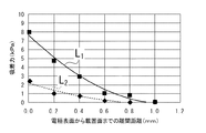
図10は電極126、127表面から載置面までの距離(離間距離)と、吸着力との関係を示すグラフであり、同図の符号L1は配線が形成された吸着対象物の吸着力の変化を示し、符号L2は配線が形成されていない場合の吸着対象物の吸着力の変化を示している。
【0010】
図10から明らかなように、配線を有する吸着対象物は配線を有しない吸着対象物に比べて吸着力が大きく、また、配線を有する場合と、配線を有しない場合のいずれの場合であっても離間距離が大きくなるほど吸着力が小さくなっている。例えば、吸着力が1kPaとなる離間距離に着目すると、配線を有しない吸着対象物では離間距離が約0.2mmであったのに対し、配線を有する吸着対象物では離間距離が約0.6mmと大きくなっている。
【0011】
これらのことから、配線のような導体を有する部分の離間距離を、導体を有しない部分よりも大きくすれば、導体を有する部分と導体を有しない部分とで吸着力の差がなくなり、吸着力の面内分布が均一となると考えられる。
【0012】
上記知見に基づいてなされた請求項1記載の発明は、装置本体を有し、前記装置本体は支持体と、前記支持体上に配置された第一の電極と、前記第一の電極に隣接して配置された第二の電極とを有し、前記装置本体の載置面上に絶縁基板を配置して前記第一の電極と前記第二の電極に正電圧と負電圧を印加すると、前記絶縁基板が吸着されるように構成された吸着装置であって、前記装置本体は、前記第一、第二の電極の上端が第一の平面に位置する凸部と、前記第一、第二の電極の上端が第二の平面に位置する凹部とを有し、前記第一の平面と前記載置面との距離は、前記第二の平面と前記載置面との距離よりも小さくされ、前記凸部は格子状に配置され、前記凹部は前記凸部の間に行列状に配置された吸着装置である。
請求項2記載の発明は、装置本体を有し、前記装置本体は支持体と、前記支持体上に配置された第一の電極と、前記第一の電極に隣接して配置された第二の電極とを有し、前記装置本体の載置面上に絶縁基板を配置して前記第一の電極と前記第二の電極に正電圧と負電圧を印加すると、前記絶縁基板が吸着されるように構成された吸着装置であって、前記装置本体は、前記第一、第二の電極の上端が第一の平面に位置する凸部と、前記第一、第二の電極の上端が第二の平面に位置する凹部とを有し、前記第一の平面と前記載置面との距離は、前記第二の平面と前記載置面との距離よりも小さくされた吸着装置によって、絶縁物領域と、前記絶縁物領域よりも導体が密集配置されたデバイス領域と、を有する前記絶縁基板を吸着する吸着方法であって、前記凹部は吸着対象の前記絶縁基板が有するデバイス領域の直下に配置し、前記凸部は吸着対象の前記絶縁基板が有する絶縁物領域の直下に配置しておく吸着方法である。
【0013】
本発明は上記のように構成されており、装置本体の凹部は、装置本体の基準となる位置からの平面的な距離が、絶縁基板の基準となる位置からデバイス領域までの平面的な距離とが等しくなる位置に形成されているので、基準となる位置同士が互いに対向するように吸着装置と絶縁基板の位置合わせを行い、絶縁基板を吸着装置に載置すると、デバイス領域が凹部上に載置されるようになっている。
【0014】
デバイス領域が位置する部分では載置面から導電膜表面までの距離が凹部の深さ分離れているので、第一、第二の電極に電圧を印加したときに発生する吸着力が小さくなる。
【0015】
【発明の実施の形態】
以下で図面を参照し、本発明の実施形態について説明する。
図1の符号1と、符号10は本発明の一実施形態の真空処理装置であるスパッタリング装置と、吸着装置をそれぞれ示している。
【0016】
図2、図3の符号20はこの吸着装置10で吸着される吸着対象物を示している。吸着対象物20は高純度石英ガラスからなる絶縁基板21を有しており、その片面には、パターニングされたITO(インジウム錫酸化物)薄膜等の導電膜が配置されている。
【0017】
導電膜は絶縁基板21の表面の所定領域に密集して形成されている。図2、3の符号25は導電膜が密集した領域であるデバイス領域を示しており、同図の符号26はデバイス領域の間に位置する領域であって、デバイス領域以外の領域である絶縁物領域を示しており、デバイス領域25は複数個互いに離間して位置している。
【0018】
ここでは、デバイス領域25は2個乃至複数個が等間隔に横一列に並べられ、横一列に並べられたデバイス領域25の一群が互いに平行に、かつ等間隔で並べれられている。即ち、絶縁基板21上のデバイス領域25は行列状に配置されている。デバイス領域25の間の格子状の部分は絶縁物領域26であり、該絶縁物領域26には導電膜が配置されていないか、あるいは、配置されていてもその密度が極少なく配置されている。
【0019】
図4はこのような20を吸着する吸着装置10の平面図を示し、図5は図4のA−A切断線断面図を、図6は図4のB−B切断線断面図をそれぞれ示している。
図4〜6を参照し、吸着装置10は装置本体14と保護層13とを有している。尚、図4では保護層13が省略されている。装置本体14は支持体11と、第一、第二の電極15a、15bと、凹部12とを有している。
【0020】
支持体11はセラミックのような絶縁材料の板で構成されている。第一、第二の電極15a、15bはタングステン(W)のような導電材料の薄膜(導電膜)で構成されており、その導電膜は支持体11の片面に密着配置されている。
【0021】
凹部12は、支持体11の導電膜が配置された面に形成された孔と、後述するように、その孔の底面上に配置された第一、第二の電極15a、15bとで構成されている。
【0022】
凹部12の支持体11上の平面的な位置は、上述したデバイス領域25の絶縁基板21上の平面的な位置と対応する位置に配置されており、上述したように、デバイス領域25は行列状に配置されているので、凹部12も行列状に配置されている。
【0023】
凹部12の周囲、又は凹部12間の部分を凸部16とすると、この凸部16は絶縁物領域26に対応して格子状になっており、凹部12の底面と凸部16の先端には第一、第二の電極15a、15bを構成する導電膜が配置されている。
【0024】
第一、第二の電極15a、15bは上述した導電膜のパターニングによってそれぞれ櫛状のパターンに形成されている。第一、第二の電極15a、15bの櫛の歯はそれぞれ複数個が設けられ、各櫛の歯は、直線状になっている。第一の電極15aの櫛状のパターンと、第二の電極15bの櫛状のパターンは互いに分離されており、第一、第二の電極15a、15bは互いに絶縁されている。
【0025】
第一、第二の電極15a、15bの櫛の歯は、凹部12が並んだ横一列の方向又は縦の一方向のいずれか一方の方向に平行に延びている。第一の電極15aの櫛の歯と第二の電極15bの櫛の歯は、凸部16上にのみ延びているものと、凸部16上と凹部12上の両方にまたがって延びているものそれぞれ両方が含まれる。
【0026】
第一の電極15aの櫛の歯部分と、第二の電極15bの櫛の歯部分は互いに噛み合うように配置されており、従って、第一の電極15aの歯と第二の電極15bの歯が交互に並んでいる。
【0027】
凸部16上のどの位置でも第一の電極15aの櫛の歯と、第二の電極15bの櫛の歯が隣接して配置されており、かつ、それらの櫛の歯の幅と間隔は一定になっている。即ち、凸部16上では、第一、第二の電極15a、15bの互いに隣接する部分が均一に分布されているので、第一、第二の電極15a、15bに正負の電圧が印加されると、凸部16を構成する支持体11上の第一、第二の電極15a、15bの表面近傍位置には均一な電界が形成されるようになっている。
【0028】
また、ここでは各凹部12内にも第一、第二の電極15a、15bが凸部16にある第一、第二の電極15a、15bと同じ間隔を空けて配置されており、凹部12を構成する支持体11上の第一、第二の電極15a、15b間の表面近傍位置には均一な電界が形成されるが、凹部12の電界は凸部16と同じ高さでは凸部16の電界よりも小さくなる。
【0029】
保護層13は二酸化ケイ素(SiO2)のような絶縁材料の薄膜で構成されている。第一、第二の電極15a、15bの表面はこの保護層13で覆われており、上述した吸着対象物20は保護層13に接触するので、第一、第二の電極15a、15bは保護されるようになっている。
【0030】
図1に示すスパッタリング装置1は真空槽2を有しており、上述した吸着装置10は保護層13が形成された面を天井側に向けられた状態で真空槽2内の底壁側に配置されている。
【0031】
上述したスパッタリング装置1を用いて吸着対象物20を処理するには、先ず、真空槽2に接続された真空排気系8を起動し、真空槽2内に所定圧力の真空雰囲気を形成した後、その真空雰囲気を維持したまま、吸着対象物20を真空槽2内に搬入する。
【0032】
吸着対象物20のデバイス領域25が形成された面を上側に向けた状態で、吸着対象物20と吸着装置10とを相対的に位置合わせし、絶縁基板21のデバイス領域25が形成された側とは反対側の面である載置面29を、凸部16上の保護層13表面に接触させ、吸着対象物20を吸着装置10上に載置すると、図7に示すように、デバイス領域25直下に凹部12が配置され、絶縁物領域26直下に凸部16が配置される。
【0033】
凸部16は支持体11の平坦な面と、膜厚一定な導電膜とで構成されるため、各凸部16の先端の導電膜表面は同じ第一の平面18に位置する。また、凹部12を構成する孔はそれぞれ深さが均一であり、凹部12はその孔と、膜厚一定な導電膜とで構成されるため、各凹部12の底面の導電膜表面はそれぞれ同じ第二の平面19に位置する。
【0034】
保護層13の膜厚は一定になっており、載置面29は凸部16上の保護層13表面に接触するため、載置面29は第一、第二の平面18、19に対して並行であり、また、接触面29から第一の平面19までの離間距離W1は接触面29から第二の平面19までの離間距離W2に比べて凹部12の深さ分だけ小さくなっている。
【0035】
上述したように、デバイス領域25のように導体密度が大きい場合の吸着力は、絶縁物領域26にように導体密度が小さい場合の吸着力よりも大きくなるが、導体密度が大きい場合であっても離間距離が大きくなれば吸着力が小さくなる。
【0036】
予め、絶縁基板21の膜厚と材質は分かっており、載置面29から第二の平面19までの離間距離W2がデバイス領域25にかかる吸着力と、絶縁物領域26にかかる吸着力が略等しくなるように、凹部12の深さが深くなっている。
【0037】
従って、静電チャック電源7を起動し、第一、第二の電極15a、15bに正負の電圧を印加すると、デバイス領域25と絶縁物領域26は同じ大きさの吸着力で吸着され、吸着対象物20は吸着装置10に安定して保持される。
【0038】
吸着装置10には不図示の加熱手段が設けられており、吸着対象物20が吸着装置10に密着した状態で吸着装置10を加熱すると、吸着対象物20が所定温度に加熱される。
【0039】
次いで、真空槽2内にアルゴン(Ar)ガスのようなスパッタガスを導入しながら、真空槽2内に所定圧力の真空雰囲気を維持し、スパッタ電源6を起動し、ターゲット5に電圧を印加すると、ターゲット5がスパッタリングされ、吸着対象物20に薄膜が成長する。
【0040】
薄膜が所定膜厚まで成長したところでスパッタリングを停止し、次いで、第一、第二の電極15a、15bへの電圧印加を停止すると、吸着力が解除され、成膜処理後の吸着対象物20を吸着装置10から持ち上げることができる。
【0041】
以上は、支持体11の孔と、膜厚が一定な導電膜とで凹部12が構成された場合について説明したが、本発明はこれに限定されるものではない。
図8の符号50は本発明他の例の吸着装置を示している。この吸着装置50は、装置本体54と、保護層53とを有している。
【0042】
装置本体54は、その表面と裏面が平坦な支持体51と、支持体51の平坦な表面に形成された第一、第二の電極55a、55bとを有しており、第一、第二の電極55a、55bを構成する導電膜の膜厚は一定ではない。
【0043】
上述した吸着装置10では、支持体11の孔と、膜厚一定な導電膜とで凹部12が構成されていたが、この吸着装置50では、導電膜の膜厚が薄い部分52と、導電膜の膜厚が厚い部分56があり、膜厚の薄い部分52は上述したような吸着対象物20のデバイス領域25に対応する位置に配置され、膜厚の厚い部分56は絶縁物領域26に対応する位置に配置されているので、吸着対象物20と吸着装置50とを相対的に位置合わせした後、第一、第二の電極55a、55b表面に形成された保護層53の表面に、載置面29を接触させ、吸着対象物20を載置すれば、膜厚の薄い部分52上にデバイス領域25が配置され、膜厚の厚い部分56上に絶縁物領域26が配置される。
【0044】
保護層53は膜厚の薄い部分52と厚い部分56を覆うように形成されている。保護層53の表面は平坦になっており、支持体51の平坦な表面から保護層53の平坦な表面までの距離は均一になっている。従って、保護層53の平坦な表面に載置面29を密着させたとき、載置面29から膜厚の厚い部分56までの距離は、載置面29から膜厚の薄い部分52までの距離よりも小さくなる。
【0045】
即ち、この吸着装置50の膜厚の薄い部分52と、膜厚の厚い部分56は、図4〜5に示した吸着装置10の凹部12と凸部16に相当する。この吸着装置50においても、膜厚の厚い部分56の先端が位置する第一の平面58から載置面29までの距離は、膜厚の薄い部分52の底面が位置する第二の平面59から載置面29までの距離が、図10に示すような、一定電圧で吸着力が等しくなる離間距離で形成できれば、吸着対象物20にかかる吸着力は面内分布が均一になる。
【0046】
図8の符号L1は保護層53の平坦な表面から、膜厚の厚い部分56の電極55a、55b表面までの距離を示し、符号L2は保護層53の平坦な表面から膜厚の薄い部分52の電極55a、55b表面までの距離を示している。例えば、図10において全面の吸着力を1kPaで均一にするためには、距離L1を0.7mm、距離L2を0.3mmにすればよい。
【0047】
以上は、吸着対象物20の絶縁基板21が、高純度石英ガラスで構成された場合について説明したが、例えば、耐熱ガラス(ここではパイレックスガラス(登録商標)、室温抵抗率1014Ω・cm)や、無アルカリガラス等他の種類のガラスや、ポリイミド樹脂やポリカーボネート樹脂等の樹脂で構成されたものを用いることができる。
【0048】
支持体11に孔を形成する場合、その形成方法は特に限定されず、ブラスト処理、ウェットエッチング等の種々の方法を用いることができる。
第一、第二の電極15a、15bを構成する導電膜はタングステンからなるものに限定されず、銅、アルミニウム、熱分解グラファイト(P−G)等種々の導電性物質からなるものを用いることができ、また、導電膜の成膜方法もCVD法、PVD法等種々の成膜方法を用いることができる。
【0049】
保護層13を構成する絶縁材料は二酸化ケイ素に限定されるものではなく、酸化アルミニウム(Al2O3)や、窒化アルミニウム(AlN)、熱分解窒化ホウ素(P−BN)等種々の絶縁材料で保護層13を構成することができる。また、保護層13、53を形成せずに、第一、第二の電極表面を露出させ、載置面29を第一、第二の電極の表面に直接接触させてもよい。
【0050】
また、以上は本発明の真空処理装置の一例として、スパッタリング装置1について説明したが、本発明はこれに限定されるものではなく、本発明の吸着装置10を有するものであれば、真空蒸着装置等の種々の成膜装置や、エッチング装置、イオン注入装置等の真空処理装置がある。また、本発明の吸着装置10に搬送機構を設ければ、吸着対象物20を吸着しながら真空処理装置間を搬送する、いわゆる搬送装置として用いることができる。
【0051】
【発明の効果】
本発明の吸着装置に吸着対象物を載置したときに、配線のような導体が密集するデバイス領域は凹部上に配置され、配線が密集しない絶縁物領域は凸部上に配置される。従って、デバイス領域では、載置面から電極表面までの距離が絶縁物領域よりも大きく、その距離はデバイス領域の吸着力が絶縁物領域と略等しくなるようになっているので、吸着力の面内分布が均一になり、吸着対象物が安定して保持される。
【図面の簡単な説明】
【図1】本発明に用いられる成膜装置の一例を説明する図
【図2】吸着対象物の一例を示す平面図
【図3】図2のZ−Z切断線断面図
【図4】本発明の一例の吸着装置の第一、第二の電極を説明するための平面図
【図5】図4のA−A切断線断面図に相当する図
【図6】図4のB−B切断線断面図に相当する図
【図7】吸着対象物を吸着装置に載置した状態を示す断面図
【図8】本発明の他の例の吸着装置を説明するための断面図
【図9】従来技術の吸着装置を説明するための断面図
【図10】離間距離と吸着力との関係を示すグラフ
【符号の説明】
20……吸着対象物 10、50……吸着装置 11、51……支持体 12、52……凹部 14、54……装置本体 15a、15b、55a、55b……第一、第二の電極 18、58……第一の平面 19、59……第二の平面 29……載置面[0001]
BACKGROUND OF THE INVENTION
The present invention relates to an electrostatic adsorption device, and more particularly, to an adsorption device that adsorbs an adsorption object having a device pattern formed on an insulating substrate.
[0002]
[Prior art]
[0003]
When an insulating substrate is placed on the surface of the
In general, when a dielectric having a polarizability α is placed in a non-uniform electric field E, a gradient force expressed by the following equation per unit area acts on the dielectric.
[0004]
f = 1/2 · α · grad (E 2 )
The first and
[0005]
The insulating substrate receives the above-described gradient force, and the entire back surface of the substrate is adsorbed on the surface of the
By the way, in the actual manufacturing process, conductors such as wiring and transistors are often formed on an insulating substrate, and when adsorbing a mixture of such a conductor and an insulator such as a glass substrate, There is a problem that the in-plane distribution of the adsorption force becomes non-uniform and the stability of adsorption is low.
[0006]
[Problems to be solved by the invention]
The present invention was created to meet the demands of the above prior art, and its purpose is to make the in-plane distribution of the suction force uniform when suctioning a suction object in which a conductor and an insulator are mixed. It is to provide an adsorption device.
[0007]
[Means for Solving the Problems]
The present inventors prepared two types of adsorption objects: an adsorption object composed of a rectangular glass substrate with a side of 50 cm and no wiring formed thereon, and an adsorption object formed with wiring formed on one surface of the glass substrate. did.
[0008]
Those objects to be attracted are arranged on the
[0009]
FIG. 10 is a graph showing the relationship between the distances (separation distances) from the surfaces of the
[0010]
As is clear from FIG. 10, the suction object having wiring has a larger suction force than the suction object having no wiring, and the case where the wiring object is provided and the case where the wiring object is not provided. However, the greater the separation distance, the smaller the attractive force. For example, when focusing attention on the separation distance at which the suction force is 1 kPa, the separation distance is about 0.2 mm for the adsorption object having no wiring, whereas the separation distance is about 0.6 mm for the adsorption object having the wiring. It is getting bigger.
[0011]
From these facts, if the separation distance of the part having a conductor such as wiring is made larger than the part having no conductor, there is no difference in the adsorption force between the part having the conductor and the part having no conductor, and the adsorption force The in-plane distribution is considered to be uniform.
[0012]
The invention according to
The invention according to
[0013]
The present invention is configured as described above, and the recess of the apparatus main body has a planar distance from a position serving as a reference of the apparatus main body to a planar distance from a position serving as a reference of the insulating substrate to the device region. Since the suction device and the insulating substrate are aligned so that the reference positions face each other, and the insulating substrate is placed on the suction device, the device region is placed on the recess. It is supposed to be placed.
[0014]
In the portion where the device region is located, the distance from the mounting surface to the surface of the conductive film is separated by the depth of the recess, so that the attractive force generated when a voltage is applied to the first and second electrodes is reduced.
[0015]
DETAILED DESCRIPTION OF THE INVENTION
Embodiments of the present invention will be described below with reference to the drawings.
[0016]
[0017]
The conductive film is densely formed in a predetermined region on the surface of the insulating
[0018]
Here, two or
[0019]
4 shows a plan view of the
4 to 6, the
[0020]
The
[0021]
The
[0022]
The planar position of the
[0023]
If the portion around the
[0024]
The first and
[0025]
The comb teeth of the first and
[0026]
The comb tooth portion of the
[0027]
The comb teeth of the
[0028]
Also, here, the first and
[0029]
The
[0030]
The
[0031]
In order to process the
[0032]
With the surface on which the
[0033]
Since the
[0034]
The film thickness of the
[0035]
As described above, the attracting force when the conductor density is large as in the
[0036]
The film thickness and material of the insulating
[0037]
Accordingly, when the electrostatic
[0038]
The
[0039]
Next, when a sputtering atmosphere such as argon (Ar) gas is introduced into the
[0040]
When the thin film has grown to a predetermined thickness, the sputtering is stopped, and then, when the voltage application to the first and
[0041]
The above describes the case where the
[0042]
The apparatus
[0043]
In the
[0044]
The
[0045]
That is, the
[0046]
Sign L 1 in FIG. 8 from the flat surface of the
[0047]
The above has described the case where the insulating
[0048]
When forming a hole in the
The conductive films constituting the first and
[0049]
The insulating material constituting the
[0050]
Moreover, although the
[0051]
【The invention's effect】
When an object to be sucked is placed on the suction device of the present invention, a device region where conductors such as wiring are densely arranged is arranged on the concave portion, and an insulating region where wiring is not densely arranged is arranged on the convex portion. Therefore, in the device area, the distance from the mounting surface to the electrode surface is larger than the insulator area, and the distance is such that the adsorption force of the device area is substantially equal to that of the insulator area. The internal distribution becomes uniform, and the adsorption object is stably held.
[Brief description of the drawings]
FIG. 1 is a diagram for explaining an example of a film forming apparatus used in the present invention. FIG. 2 is a plan view showing an example of an object to be adsorbed. FIG. 3 is a sectional view taken along the line ZZ in FIG. The top view for demonstrating the 1st, 2nd electrode of the adsorption | suction apparatus of an example of invention. FIG. 5 The figure corresponded in AA cut-line sectional drawing of FIG. FIG. 7 is a cross-sectional view showing a state where an object to be sucked is placed on the suction device. FIG. 8 is a cross-sectional view for explaining a suction device according to another example of the present invention. Sectional drawing for demonstrating the adsorption apparatus of a prior art [FIG. 10] The graph which shows the relationship between a separation distance and adsorption | suction power
20 ……
Claims (2)
前記装置本体は支持体と、前記支持体上に配置された第一の電極と、前記第一の電極に隣接して配置された第二の電極とを有し、
前記装置本体の載置面上に絶縁基板を配置して前記第一の電極と前記第二の電極に正電圧と負電圧を印加すると、前記絶縁基板が吸着されるように構成された吸着装置であって、
前記装置本体は、前記第一、第二の電極の上端が第一の平面に位置する凸部と、前記第一、第二の電極の上端が第二の平面に位置する凹部とを有し、
前記第一の平面と前記載置面との距離は、前記第二の平面と前記載置面との距離よりも小さくされ、
前記凸部は格子状に配置され、前記凹部は前記凸部の間に行列状に配置された吸着装置。Having a device body,
The apparatus main body includes a support, a first electrode disposed on the support, and a second electrode disposed adjacent to the first electrode,
An adsorption apparatus configured to adsorb the insulating substrate when an insulating substrate is disposed on the mounting surface of the apparatus body and a positive voltage and a negative voltage are applied to the first electrode and the second electrode. Because
The apparatus main body includes a convex portion in which upper ends of the first and second electrodes are located on a first plane, and a concave portion in which upper ends of the first and second electrodes are located on a second plane. ,
The distance between the first plane and the placement surface is smaller than the distance between the second plane and the placement surface ,
The adsorption device in which the convex portions are arranged in a lattice pattern and the concave portions are arranged in a matrix between the convex portions .
前記装置本体は支持体と、前記支持体上に配置された第一の電極と、前記第一の電極に隣接して配置された第二の電極とを有し、
前記装置本体の載置面上に絶縁基板を配置して前記第一の電極と前記第二の電極に正電圧と負電圧を印加すると、前記絶縁基板が吸着されるように構成された吸着装置であって、
前記装置本体は、前記第一、第二の電極の上端が第一の平面に位置する凸部と、前記第一、第二の電極の上端が第二の平面に位置する凹部とを有し、
前記第一の平面と前記載置面との距離は、前記第二の平面と前記載置面との距離よりも小さくされた吸着装置によって、絶縁物領域と、前記絶縁物領域よりも導体が密集配置されたデバイス領域と、を有する前記絶縁基板を吸着する吸着方法であって、
前記凹部は吸着対象の前記絶縁基板が有するデバイス領域の直下に配置し、
前記凸部は吸着対象の前記絶縁基板が有する絶縁物領域の直下に配置しておく吸着方法。 Having a device body,
The apparatus main body includes a support, a first electrode disposed on the support, and a second electrode disposed adjacent to the first electrode,
An adsorption apparatus configured to adsorb the insulating substrate when an insulating substrate is disposed on the mounting surface of the apparatus body and a positive voltage and a negative voltage are applied to the first electrode and the second electrode. Because
The apparatus main body includes a convex portion in which upper ends of the first and second electrodes are located on a first plane, and a concave portion in which upper ends of the first and second electrodes are located on a second plane. ,
The distance between the first plane and the placement surface is such that the conductor is more than the insulator region and the insulator region by a suction device that is smaller than the distance between the second plane and the placement surface. A method of adsorbing the insulating substrate having densely arranged device regions,
The concave portion is disposed immediately below a device region of the insulating substrate to be attracted,
The said convex part is the adsorption | suction method arrange | positioned directly under the insulator area | region which the said insulated substrate of adsorption | suction object has.
Priority Applications (1)
| Application Number | Priority Date | Filing Date | Title |
|---|---|---|---|
| JP2002309646A JP4101017B2 (en) | 2002-10-24 | 2002-10-24 | Adsorption device and adsorption method |
Applications Claiming Priority (1)
| Application Number | Priority Date | Filing Date | Title |
|---|---|---|---|
| JP2002309646A JP4101017B2 (en) | 2002-10-24 | 2002-10-24 | Adsorption device and adsorption method |
Publications (2)
| Publication Number | Publication Date |
|---|---|
| JP2004146585A JP2004146585A (en) | 2004-05-20 |
| JP4101017B2 true JP4101017B2 (en) | 2008-06-11 |
Family
ID=32455394
Family Applications (1)
| Application Number | Title | Priority Date | Filing Date |
|---|---|---|---|
| JP2002309646A Expired - Lifetime JP4101017B2 (en) | 2002-10-24 | 2002-10-24 | Adsorption device and adsorption method |
Country Status (1)
| Country | Link |
|---|---|
| JP (1) | JP4101017B2 (en) |
Families Citing this family (2)
| Publication number | Priority date | Publication date | Assignee | Title |
|---|---|---|---|---|
| US7940511B2 (en) * | 2007-09-21 | 2011-05-10 | Asml Netherlands B.V. | Electrostatic clamp, lithographic apparatus and method of manufacturing an electrostatic clamp |
| EP3707747A4 (en) | 2017-11-10 | 2021-07-28 | Applied Materials, Inc. | Patterned chuck for double-sided processing |
-
2002
- 2002-10-24 JP JP2002309646A patent/JP4101017B2/en not_active Expired - Lifetime
Also Published As
| Publication number | Publication date |
|---|---|
| JP2004146585A (en) | 2004-05-20 |
Similar Documents
| Publication | Publication Date | Title |
|---|---|---|
| JP4030350B2 (en) | Split electrostatic chuck | |
| TWI314759B (en) | Rf grounding of cathode in process chamber | |
| TWI669772B (en) | Transparent electrostatic carrier | |
| WO2000072376A1 (en) | Electrostatic chuck and treating device | |
| JP4339306B2 (en) | Adsorption method | |
| JP2002520877A5 (en) | ||
| KR102110749B1 (en) | Apparatus for holding a substrate in a vacuum deposition process, a system for depositing a layer on a substrate, and a method for holding a substrate | |
| JP2521471B2 (en) | Electrostatic suction device | |
| JP4774025B2 (en) | Adsorption device, transfer device | |
| JP4101017B2 (en) | Adsorption device and adsorption method | |
| JP4030361B2 (en) | Electrostatic adsorption method | |
| KR102104471B1 (en) | Thin film transistor, gate drive on array and display apparatus having the same, and fabricating method thereof | |
| JP2002345273A (en) | Electrostatic chuck | |
| KR100830237B1 (en) | A structure for susceptor in large area substrate processing system | |
| JP4024613B2 (en) | Adsorption device, vacuum processing device and adsorption method | |
| JP4676098B2 (en) | Adsorption device | |
| WO2003032402A1 (en) | Mems hybrid structure having flipped silicon with external standoffs | |
| JP2003133400A (en) | Attraction apparatus, vacuum processing apparatus, and method for manufacturing the suction apparatus | |
| TWI700774B (en) | Vacuum apparatus, vacuum-suction device and conductive thin film manufacturing method | |
| JP4342691B2 (en) | Electrostatic adsorption device and vacuum processing device | |
| JP2006054445A (en) | Attracting device | |
| JP4166379B2 (en) | Substrate transfer device | |
| JP2004047912A (en) | Sucking device and vacuum processing device | |
| JP2002339061A (en) | Thin film depositing method | |
| JPH11233600A (en) | Electrostatic attractor and vacuum processor using the same |
Legal Events
| Date | Code | Title | Description |
|---|---|---|---|
| A621 | Written request for application examination |
Free format text: JAPANESE INTERMEDIATE CODE: A621 Effective date: 20050622 |
|
| A977 | Report on retrieval |
Free format text: JAPANESE INTERMEDIATE CODE: A971007 Effective date: 20070926 |
|
| A131 | Notification of reasons for refusal |
Free format text: JAPANESE INTERMEDIATE CODE: A131 Effective date: 20071002 |
|
| A521 | Written amendment |
Free format text: JAPANESE INTERMEDIATE CODE: A523 Effective date: 20071128 Free format text: JAPANESE INTERMEDIATE CODE: A821 Effective date: 20071128 |
|
| A131 | Notification of reasons for refusal |
Free format text: JAPANESE INTERMEDIATE CODE: A131 Effective date: 20071225 |
|
| A521 | Written amendment |
Free format text: JAPANESE INTERMEDIATE CODE: A821 Effective date: 20080220 Free format text: JAPANESE INTERMEDIATE CODE: A523 Effective date: 20080220 |
|
| TRDD | Decision of grant or rejection written | ||
| A01 | Written decision to grant a patent or to grant a registration (utility model) |
Free format text: JAPANESE INTERMEDIATE CODE: A01 Effective date: 20080318 |
|
| A61 | First payment of annual fees (during grant procedure) |
Free format text: JAPANESE INTERMEDIATE CODE: A61 Effective date: 20080318 |
|
| FPAY | Renewal fee payment (event date is renewal date of database) |
Free format text: PAYMENT UNTIL: 20110328 Year of fee payment: 3 |
|
| R150 | Certificate of patent or registration of utility model |
Ref document number: 4101017 Country of ref document: JP Free format text: JAPANESE INTERMEDIATE CODE: R150 Free format text: JAPANESE INTERMEDIATE CODE: R150 |
|
| FPAY | Renewal fee payment (event date is renewal date of database) |
Free format text: PAYMENT UNTIL: 20110328 Year of fee payment: 3 |
|
| FPAY | Renewal fee payment (event date is renewal date of database) |
Free format text: PAYMENT UNTIL: 20140328 Year of fee payment: 6 |
|
| R250 | Receipt of annual fees |
Free format text: JAPANESE INTERMEDIATE CODE: R250 |
|
| R250 | Receipt of annual fees |
Free format text: JAPANESE INTERMEDIATE CODE: R250 |
|
| R250 | Receipt of annual fees |
Free format text: JAPANESE INTERMEDIATE CODE: R250 |
|
| R250 | Receipt of annual fees |
Free format text: JAPANESE INTERMEDIATE CODE: R250 |
|
| R250 | Receipt of annual fees |
Free format text: JAPANESE INTERMEDIATE CODE: R250 |
|
| R250 | Receipt of annual fees |
Free format text: JAPANESE INTERMEDIATE CODE: R250 |
|
| R250 | Receipt of annual fees |
Free format text: JAPANESE INTERMEDIATE CODE: R250 |