JP4100256B2 - Communication method and information processing apparatus - Google Patents
Communication method and information processing apparatus Download PDFInfo
- Publication number
- JP4100256B2 JP4100256B2 JP2003151790A JP2003151790A JP4100256B2 JP 4100256 B2 JP4100256 B2 JP 4100256B2 JP 2003151790 A JP2003151790 A JP 2003151790A JP 2003151790 A JP2003151790 A JP 2003151790A JP 4100256 B2 JP4100256 B2 JP 4100256B2
- Authority
- JP
- Japan
- Prior art keywords
- cpu
- data
- communication
- disk cache
- processor
- Prior art date
- Legal status (The legal status is an assumption and is not a legal conclusion. Google has not performed a legal analysis and makes no representation as to the accuracy of the status listed.)
- Expired - Fee Related
Links
Images


Classifications
-
- G—PHYSICS
- G06—COMPUTING OR CALCULATING; COUNTING
- G06F—ELECTRIC DIGITAL DATA PROCESSING
- G06F12/00—Accessing, addressing or allocating within memory systems or architectures
- G06F12/02—Addressing or allocation; Relocation
- G06F12/08—Addressing or allocation; Relocation in hierarchically structured memory systems, e.g. virtual memory systems
- G06F12/0802—Addressing of a memory level in which the access to the desired data or data block requires associative addressing means, e.g. caches
- G06F12/0866—Addressing of a memory level in which the access to the desired data or data block requires associative addressing means, e.g. caches for peripheral storage systems, e.g. disk cache
- G06F12/0871—Allocation or management of cache space
-
- G—PHYSICS
- G06—COMPUTING OR CALCULATING; COUNTING
- G06F—ELECTRIC DIGITAL DATA PROCESSING
- G06F12/00—Accessing, addressing or allocating within memory systems or architectures
- G06F12/02—Addressing or allocation; Relocation
- G06F12/08—Addressing or allocation; Relocation in hierarchically structured memory systems, e.g. virtual memory systems
- G06F12/0802—Addressing of a memory level in which the access to the desired data or data block requires associative addressing means, e.g. caches
- G06F12/0806—Multiuser, multiprocessor or multiprocessing cache systems
- G06F12/084—Multiuser, multiprocessor or multiprocessing cache systems with a shared cache
-
- G—PHYSICS
- G06—COMPUTING OR CALCULATING; COUNTING
- G06F—ELECTRIC DIGITAL DATA PROCESSING
- G06F2212/00—Indexing scheme relating to accessing, addressing or allocation within memory systems or architectures
- G06F2212/60—Details of cache memory
- G06F2212/601—Reconfiguration of cache memory
- G06F2212/6012—Reconfiguration of cache memory of operating mode, e.g. cache mode or local memory mode
-
- G—PHYSICS
- G06—COMPUTING OR CALCULATING; COUNTING
- G06F—ELECTRIC DIGITAL DATA PROCESSING
- G06F3/00—Input arrangements for transferring data to be processed into a form capable of being handled by the computer; Output arrangements for transferring data from processing unit to output unit, e.g. interface arrangements
- G06F3/06—Digital input from, or digital output to, record carriers, e.g. RAID, emulated record carriers or networked record carriers
- G06F3/0601—Interfaces specially adapted for storage systems
- G06F3/0628—Interfaces specially adapted for storage systems making use of a particular technique
- G06F3/0655—Vertical data movement, i.e. input-output transfer; data movement between one or more hosts and one or more storage devices
- G06F3/0656—Data buffering arrangements
Landscapes
- Engineering & Computer Science (AREA)
- Theoretical Computer Science (AREA)
- Physics & Mathematics (AREA)
- General Engineering & Computer Science (AREA)
- General Physics & Mathematics (AREA)
- Memory System Of A Hierarchy Structure (AREA)
- Multi Processors (AREA)
Description
【0001】
【発明の属する技術分野】
本発明は、高速でセキュアな通信を行うために、ディスク装置内部に持つディスクキャッシュを介して、複数CPU間でデータの授受を行うことを特徴とした通信方法に関する
【0002】
【従来の技術】
【特許文献1】
特開2002-23958号
ビジネス向けストレージシステムには高信頼性が求められており、複数プロセッサの間でお互いの監視を行い、あるプロセッサに障害が発生したときには、他のプロセッサが障害プロセッサの作業を肩代わりすることで、通常動作を続けるシステムとなっている。複数プロセッサ間での監視は、一般的に現在時刻等の情報を定期的にやり取りするハートビートと呼ばれる通信を行う。一定時間ハートビート通信の応答がなくなると、対象プロセッサがダウンしたと考え、作業の移行を行う。また、ハートビート通信に限らず、システムの構成情報といった内部プロセッサ間で通信の行われるデータは多い。これらの通信は、一般的には外部ネットワークを用いてデータのやりとりが行われる。外部ネットワークを用いずに内部通信を行うには、内部ネットワークを用いる方法があるが、スペースの関係からあまり高速な内部ネットワークを張るのは難しい。
【0003】
【発明が解決しようとする課題】
複数プロセッサ間の通信に対して、外部ネットワークを用いる場合、通信データが外に流れるため、セキュリティ上問題になりやすい。外部ネットワークを使用しない場合には、特別に内部に専用ネットワークを結ぶ必要があり、不要なコストがかかる。本発明では、複数のプロセッサから共通してアクセスできるディスクキャッシュを介してデータのやり取りを行うことで、外部ネットワークを用いないセキュアな通信を、改めて専用ネットワークを張ることなく実現することを目的とする。ディスクキャッシュを介して複数プロセッサ間で通信を行う従来技術に特開2002-23958がある。これは、メインフレームホストが通信データをディスクキャッシュ上に常駐させ、オープン系ホストがそれを読み込むことで通信を行う方式である。この方式では、メインフレームホストとオープン系ホストは異なるシステムであり、オープン系ホストとディスクキャッシュとの間の接続を外部ネットワークを介する点で、セキュリティ上の問題が発生しうる。また、通信の方向もメインフレームホストからオープン系ホストへの一方向であり、双方向通信が不可能である。
【0004】
【課題を解決するための手段】
上記課題を解決するために本願発明の提案する通信方法は、複数のCPUと、そのCPUからアクセス可能な共有メモリを含むコンピュータシステムにおける通信方法において、共有メモリの一部を通信バッファとして割当てるステップと、複数のCPUのうちいずれかが当該通信バッファに転送データを格納済みであるかどうかを判定するステップと、通信バッファに転送データが格納されていなければ複数のCPUのうちいずれかのCPUが通信バッファに転送データを格納するステップと、バッファにデータが格納されていれば複数のCPUのうちいずれかのCPUがバッファから転送データを読み込むステップと、複数のCPUのうちいずれかのCPUがバッファから転送データを読み込んだ後、バッファを転送データが格納されていない状態とするステップを有する。
【0005】
例えばディスクキャッシュは共有メモリとして用いるのに好適である。本発明では、共有メモリの一部を通信バッファとして割り当て、通信バッファを例えばデータ転送領域と転送フラグ領域の組として管理する。データ転送領域にはCPU間で転送されるべきデータが格納される。転送フラグ領域はデータ転送領域に転送されるべきデータがあるかどうか示すフラグを格納する。例えば何もデータが入っていない領域のフラグは「0」とする。ある領域にCPUからデータが転送され、かつ、そのデータがまだ他のCPUによって読み出されていない場合、その領域のフラグは「1」とする。その領域のデータが他のCPUによって読み出された場合、その領域のフラグは「0」とする。すなわち、この例では、転送すべきデータが格納されている領域は「1」、転送すべきデータが格納されておらず、CPUが通信バッファとして使用できる領域を「0」としている。
【0006】
CPU間でデータを転送しようとする場合には、まず、転送するデータを格納できる通信バッファの領域を検出する。上の例ではフラグが「0」の領域を探す。そして、フラグが「0」の領域に転送しようとするデータを格納し、フラグを「1」とする。このフラグをチェックすることにより、当該領域に他のデータが上書きされることを防止する。各領域のフラグは定期的にあるいは所定命令を契機としてチェックされ、フラグが「1」の領域のデータは転送先CPUへ読み出される。読み出しの後、フラグは「0」とされて通信バッファ領域はクリアされる。
【0007】
これらの動作はCPUあるいはI/Oプロセッサ上で動作するソフトウェアにより実現可能である。さらに、専用のハードウェアで構成することも可能である。
【0008】
本発明の他の例である情報処理装置は、I/O命令を発行する少なくとも二つ以上のCPUと、CPUから直接的または間接的にアクセス可能なディスク装置と、ディスク装置のデータの少なくとも一部のコピーを格納するディスクキャッシュと、ディスク装置およびディスクキャッシュを制御するためのI/Oプロセッサとを有し、CPUは前記I/Oプロセッサ対してディスクキャッシュの一部領域の割当要求を行う機能を有し、I/Oプロセッサは割当要求を受けるとディスクキャッシュの一部の領域を通信バッファとして割り当てる機能を有し、任意のCPUが通信バッファにデータを書き込み、書き込んだCPUとは異なるCPUがデータを読み込む通信手段を有する。
【0009】
通信手段として、CPUまたはI/Oプロセッサは、通信バッファにこれから転送されるデータが格納されているかどうかを判定する手段と、通信バッファにこれから転送されるデータが格納されていなければ任意のCPUから転送データを通信バッファに転送して格納する手段と、通信バッファにこれから転送されるデータが格納されていれば任意のCPUが通信バッファから転送データを読み込む手段と、バッファをクリアする手段を有する。ディスクキャッシュは、プロセッサがディスクI/Oを行った際に最新データを高速なメモリ上に配置し、アクセス性能を向上するためのものである。そのため、プロセッサからディスクキャッシュにアクセスするには、ディスクI/Oを行う必要があり、またその際に書き込まれるキャッシュのアドレスを指定することはできない。本発明の一例では、特別なコマンドをディスク制御用プロセッサに対して発行することで、ディスクにアクセスすることなしにディスクキャッシュの特定領域にアクセスすることを可能とし、その特定領域に送信側プロセッサが書き込んだデータを受信側プロセッサが読み込むことで、複数プロセッサ間での通信を行う。それにより高速でセキュアな通信を可能とする。
【0010】
【発明の実施の形態】
[実施例1]
本発明の第一の実施例を説明する。
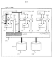
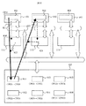
図1は本発明を説明する概念図である。101〜103はCPU、111〜113はディスクおよびディスクキャッシュを制御するI/O用プロセッサ(IOP)、121〜123はI/O用BUS、131はディスクキャッシュ、141〜142はディスクである。全てのCPU101〜103は共通のディスクキャッシュ131とBUS121〜123を介して接続されている。これら全体で一つのストレージ装置を構成している。CPU101〜103がI/Oを行うと、IOP111〜113はディスクキャッシュ131に対するキャッシュ制御を行い、ディスク141〜142にアクセスする。このとき、CPU101〜103はディスクキャッシュ131を制御することはできず、その特定領域を指定してアクセスすることはできない。そこでまず、CPU101〜103はIOP111〜113に対してディスクキャッシュ131の一部領域の割当要求を行う(151)。IOP111〜113は割当要求を受けるとディスクキャッシュ131の一部の領域132をCPU101〜103のメモリ空間に割り当てることにより、CPU101〜103が直接ディスクキャッシュ131にアクセスすることを可能とする(152)。CPU101〜103が直接ディスクキャッシュ131にアクセスすることが可能になると、各CPU間、例えばCPU101とCPU102との間の通信は、CPU101がディスクキャッシュ131の特定領域に書き込んだデータをCPU102が読み込むことで実現可能となる(153)。このとき、ディスクキャッシュ131に書き込んだデータはディスク141〜142に反映する必要はない。
【0011】
図2はCPUのアドレス空間の概要を示す。CPU101〜103のアドレス空間201はCPUのメモリ領域202を指している。それに対して、CPU101〜103がIOP111〜113に割当要求を行うと、ディスクキャッシュ131の一部領域132をCPUのアドレス空間201の一部領域203に割り当てる。これにより、CPU101〜103はアドレス空間201のうちの特定領域203にアクセスすることで、直接ディスクキャッシュ内の領域132にデータの読み書きが可能となる。IOP111〜113を介さずに、CPU101〜103がディスクキャッシュ131に直接アクセスするため、ディスクキャッシュ131へのアクセスはディスクI/Oコマンドで行うのではなく、メモリへのアクセスコマンドで行う。そのためディスクキャッシュ131にデータを書き込んでもディスク141〜142にデータは反映されない。また、CPU101〜103が直接アクセスできるディスクキャッシュ内の領域132は、ディスクI/O時にキャッシュ領域として使用できない。
上記の例は、ディスクキャッシュの一部をCPUのアドレス空間にマッピングすることで、CPUから直接ディスクキャッシュにデータの読み書きを行う方式である。
【0012】
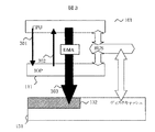
図3は他の方式の例である。図3のように通信に使用するディスクキャッシュのアドレスを指定して、DMAを用いてデータの転送を行う方式も可能である。CPU101はIOP111に対して、ディスクキャッシュの一部の領域を通信領域として割り当てることを特別のI/Oコマンドで依頼する(301)。通常の装置ではI/OプロセッサへのI/Oコマンドはディスクアクセスのためのものであるが、本発明では、ディスクアクセスではなくCPU間データ転送用のI/Oコマンドを用いる。それを受けて、IOP111はディスクキャッシュの一部領域132を通信領域として割り当て、CPU101に対してそのアドレスとサイズを通知する(302)。以降、通信領域として割り当てられた領域は、CPU101が自由に使用でき、アドレスとサイズを指定して通信データをDMA転送することができる(303)。通信領域として割り当てる領域は、ディスクI/Oに対するキャッシュ領域として使用しない特別な領域であるか、あるいは通常の領域であれば以降、キャッシュ領域として使用しないようIOP111で制御することが必要である。図4はCPU間通信の概要を示す。CPUから直接アクセスするディスクキャッシュ領域132に通信バッファ411〜416を用意する。本実施例では、全CPU間で双方向の通信を行うため、それぞれの通信用に別の通信バッファを設けた。例えば、CPU101からCPU102にデータ転送を行う場合、通信バッファ411を用いる。CPU101は転送データ401を通信バッファ311に書込み、CPU102は通信バッファ411のデータを受信領域402に読み込む。
【0013】
図5は通信バッファの概念を示す。通信バッファは図5のように内部が複数のメッセージキューに分かれており、先頭から順にラウンドロビンに使用する。各メッセージキューには転送フラグ領域501と転送データを書き込む領域502が存在し、送信CPU101は転送フラグ領域501にフラグがたっていないのを確認して転送データ領域502にデータを転送し、転送完了後転送フラグ領域501にフラグをたてる。受信CPU102は転送フラグ領域501にフラグがたっているメッセージキューを検索し、転送データ領域502から受信バッファ402にデータを読み込む。読み込み完了後転送フラグ領域501のフラグを落とす。メッセージキューは先頭から順に使用するため、送受信CPUとも前回使用したキューの位置を記憶しておくことにより、通信時に確認すべき転送フラグ領域501の位置は一意に定まる。
【0014】
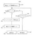
図6は本実施例の送信処理のフローチャートである。送信CPUが転送フラグ領域を読み込み(601)、メッセージキューの使用状況を確認する(602)。メッセージキューが全て使用中であれば、タイムアウトするまでキューが開放されるのをチェックし(606)、タイムアウト時間内にキューが開放されなければネットワークBUSYでエラー終了となる(607)。一方、602において、空きバッファが見つかれば転送データをバッファに書き込む(603)。転送データ書込み後、転送フラグ領域にフラグをセットし(604)、送信を完了する(605)。
【0015】
図7に受信処理のフローチャートを示す。受信CPUは転送フラグ領域を読み込み(701)、転送データが書き込まれたか確認する(702)。転送フラグがたっていなければそのまま終了し(705)、たっていれば当該バッファより転送データを読み込む(703)。読み込み完了後転送フラグをクリアし(704)、受信処理を終了する(706)。受信CPUが転送フラグ領域の読み込みを行う契機は、定期的に読み込みを繰り返す方式と、ディスクキャッシュ上の通信領域にデータが書き込まれるとCPUにハードまたはソフト割り込みをあげる方式がある。
[実施例2]
次に本発明の第二の実施例について説明する。第二の実施例は、CPUが直接ディスクキャッシュにアクセスせず、ディスクキャッシュの制御をIOPに依頼する点が特徴的である。すなわちCPUは転送データのアドレスをIOPに通知し、IOPがディスクキャッシュを介して受信CPUにデータを転送する方式である。
ディスクキャッシュ上の通信バッファの仕様は図4、5と同一である。CPUからは直接ディスクキャッシュをアクセスできないため、メッセージキューへの書き込みはIOPを経由して行う。
【0016】
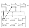
図8に本実施例の概要を示す。CPU101は転送データの格納されるメモリ801のアドレスをIOP111に通知する(821)。転送データはCPU101に内蔵されるあるいは外付けされるメモリ801内に格納されている。CPU101からの通知を受けたIOP111はメモリ801から転送データをディスクキャッシュ上の通信バッファ811に転送する(822)。受信CPU102はIOP112に転送データを受信するメモリ802のアドレスを通知する(823)。CPU102からの通知を受けたIOP112は通信バッファ811からメモリ802にデータ転送する(824)。送受信IOP間のメッセージキューの管理方法は第一の実施例におけるCPU間のメッセージキューの管理方法と同一である。すなわち、送信IOP111は通信バッファ811内の転送フラグを確認し、空きバッファを検索する。検索した空きバッファにデータの書き込みを行い、転送フラグにフラグを立てる。受信IOP112は転送フラグを確認し、データ到着を検出すると通信バッファからデータを読み込み受信バッファ802に格納する。最後に転送フラグを落とす。CPUのローカルメモリ801-803にディスクキャッシュ上のメッセージキューと同様に、送受信先ごとにメッセージキューを用意し、先頭から順にキューを使用することとすれば、CPUからIOPに対して発行する通信要求には送受信データのアドレスを指定する必要はない。
例えば、CPU101のローカルメモリ801には、送信キューとしてCPU1からCPU2への送信キュー(ディスクキャッシュ132の811に対応する)、CPU1からCPU3への送信キュー(ディスクキャッシュ132の816に対応する)、CPU1からCPU4への送信キュー・・・を設け、また、受信キューとしてCPU2からCPU1への受信キュー(ディスクキャッシュ132の812に対応する)、CPU3からCPU1への受信キュー(ディスクキャッシュ132の815に対応する)、CPU4からCPU1への受信キュー・・・を設ける。他のローカルメモリ802、803,...も同様である。
この場合、送信CPUが送信要求をIOPに通知すると、IOPはCPUローカルメモリ801のキューからディスクキャッシュ132の対応するキューにデータ転送する。このとき、ローカルメモリ801とディスクキャッシュ132の各キューはラウンドロビンで順番に使用される。
【0017】
また、受信IOPはディスクキャッシュ132上のメッセージキューが更新されたのを契機として受信バッファに転送データを格納する。このとき、ディスクキャッシュ132のキューからCPUローカルメモリ802の対応するキューにデータ転送する。このときも、各キューはラウンドロビンで順番に使用される。その後、受信CPUにデータ格納完了を通知する。
以上の構成によれば、キューは順番に使用されるので、CPUからIOPに対して発行する通信要求には送受信データのアドレスを指定する必要はない。
CPUからIOPへの通信要求は特別なI/Oコマンドを用いて行われる。通常I/Oコマンドは、コマンド種別(READ/WRITE)、CPUのローカルメモリアドレス、ディスクのアドレス等の情報を含んでいる。これらの情報を元にIOPはCPUローカルメモリアドレスにあるデータをディスクアドレスに書き込み、あるいは逆に読み込みを行う。本実施例では、コマンドのI/Fは通常I/Oコマンドと同一のまま、コマンド種別に通常のREAD/WRITEではなく、送信/受信を示す特別なコマンド種別を指定することで、IOPは通信要求であると判定することが可能である。本発明では通信用のディスクキャッシュに書き込まれるデータは、通信相手CPUに対して転送するためのもので、ディスクに反映する必要はない。したがって、IOPは送信要求を示す特別なコマンドが渡されると、ディスクにI/Oせずにディスクキャッシュにのみデータを反映させるという特別な処理を行う。受信CPUから受信要求コマンドが渡されると、同様にディスクからI/Oせずにキャッシュから直接データを読み込む。本実施例において、CPUからIOPに発行する通信要求は特別なI/Oコマンドとするのではなく、特別なアドレスへのI/Oコマンドを発行することで通信要求とすること、あるいは通信デバイスとして通常のネットワークデバイスではなく、特別に用意した仮想デバイスを指定して通信を発行することで通信要求とすることもできる。
【0018】
上記二つの実施例では、送受信処理をそれぞれ独立に扱い、受信処理の発生契機を受信関数のコールまたはデータ到着の認識としている。それに対して、第三の実施例として送信CPUが送信開始後、受信CPUに対して通信開始を通知する方式もある。ディスクキャッシュの特定領域にデータを書き込むと受信CPUに割込みが発生するする仕組みを用意し、送信CPUが転送データをディスクキャッシュに書き込み後、割り込み発生領域に書き込むことで受信CPUに通知する。あるいは、ディスクキャッシュより小容量で高速なネットワークあるいは共有メモリを用意し、送信開始通知を高速パスで送ることで受信CPUに通知する。割込みまたは別パスで送信開始通知を受けた受信CPUは、それを契機に受信処理を開始する。
【0019】
【発明の効果】
本発明では、ディスクキャッシュの一部の領域をCPUから直接アクセスすることを可能とし、ディスクキャッシュ上に通信用のバッファを配置する。送信CPUがディスクキャッシュ上の通信バッファに書き込んだデータを受信CPUが読み込むことで通信を実現できる。ディスクキャッシュは、ディスクI/O高速化のため標準的に用意されており、全CPUから共通してアクセスすることが可能である。このため新たな装置を用意することなく、全CPU間での双方向通信が可能となる。また、内部バスを介してデータ転送を行うため、外部からデータが見えず、セキュアな通信が可能となる。通信コマンドは一般的なI/Oコマンドと同一フォーマットであり、新たなI/Fを必要としない。
【図面の簡単な説明】
【図1】本発明の実施例を示した概略ブロック図である。
【図2】ディスクキャッシュのCPUアドレス空間へのマッピングを示す概念図である。
【図3】ディスクキャッシュへのアクセスをDMAで行う方式を示すブロック図である。
【図4】実施例のデータ転送方法を示すブロック図である。
【図5】ディスクキャッシュ上のメッセージキューの構成図である。
【図6】実施例の送信処理の流れ図である。
【図7】実施例の受信処理の流れ図である。
【図8】別の実施例におけるデータ転送方法を示すブロック図である。
【符号の説明】
101〜103…CPU
111〜113…IOP
121〜123…データバス
131…ディスクキャッシュ
132…ディスクキャッシュのうち通信に使用する領域
141〜142…ディスク
151〜153…通信処理の流れ。[0001]
BACKGROUND OF THE INVENTION
The present invention relates to a communication method characterized in that, in order to perform high-speed and secure communication, data is exchanged between a plurality of CPUs via a disk cache provided in the disk device.
[Prior art]
[Patent Document 1]
JP 2002-23958 A business storage system is required to have high reliability, and multiple processors monitor each other. When a failure occurs in one processor, the other processor does the work of the failed processor. By taking over, it is a system that continues normal operation. Monitoring between a plurality of processors generally performs communication called heartbeat for exchanging information such as current time periodically. If there is no heartbeat communication response for a certain period of time, the target processor is considered to have gone down, and work is transferred. In addition to heartbeat communication, there is much data that is communicated between internal processors, such as system configuration information. In these communications, data is generally exchanged using an external network. In order to perform internal communication without using an external network, there is a method using an internal network, but it is difficult to set up a very high-speed internal network because of space.
[0003]
[Problems to be solved by the invention]
When an external network is used for communication between a plurality of processors, communication data flows outside, which is likely to cause a security problem. When an external network is not used, it is necessary to connect a dedicated network inside, and there is an unnecessary cost. An object of the present invention is to realize secure communication without using an external network without establishing a dedicated network by exchanging data via a disk cache that can be accessed in common by a plurality of processors. . Japanese Patent Laid-Open No. 2002-23958 is a conventional technique for performing communication between a plurality of processors via a disk cache. In this method, communication is performed by a mainframe host having communication data resident on a disk cache and an open host reading it. In this method, the mainframe host and the open system host are different systems, and a security problem may occur in that the connection between the open system host and the disk cache is via an external network. Also, the communication direction is one direction from the mainframe host to the open host, and bi-directional communication is impossible.
[0004]
[Means for Solving the Problems]
In order to solve the above problems, a communication method proposed by the present invention includes a step of allocating a part of a shared memory as a communication buffer in a communication method in a computer system including a plurality of CPUs and a shared memory accessible from the CPUs. Determining whether any of the plurality of CPUs has stored the transfer data in the communication buffer; and if no transfer data is stored in the communication buffer, one of the plurality of CPUs communicates A step of storing the transfer data in the buffer, a step of reading one of the plurality of CPUs from the buffer if the data is stored in the buffer, and a step of reading one of the plurality of CPUs from the buffer. After the transfer data is read, there is a step of setting the buffer to a state where no transfer data is stored.
[0005]
For example, a disk cache is suitable for use as a shared memory. In the present invention, a part of the shared memory is allocated as a communication buffer, and the communication buffer is managed as a set of, for example, a data transfer area and a transfer flag area. Data to be transferred between CPUs is stored in the data transfer area. The transfer flag area stores a flag indicating whether there is data to be transferred to the data transfer area. For example, the flag of an area that contains no data is set to “0”. When data is transferred from a CPU to a certain area and the data has not yet been read out by another CPU, the flag of that area is set to “1”. When the data of the area is read by another CPU, the flag of the area is set to “0”. That is, in this example, the area where the data to be transferred is stored is “1”, and the area where the data to be transferred is not stored and can be used as a communication buffer by the CPU is “0”.
[0006]
When data is to be transferred between CPUs, a communication buffer area that can store data to be transferred is first detected. In the above example, an area whose flag is “0” is searched. Then, the data to be transferred is stored in the area where the flag is “0”, and the flag is set to “1”. Checking this flag prevents other data from being overwritten in the area. The flag of each area is checked periodically or triggered by a predetermined instruction, and the data of the area whose flag is “1” is read to the transfer destination CPU. After reading, the flag is set to “0” and the communication buffer area is cleared.
[0007]
These operations can be realized by software operating on a CPU or an I / O processor. Furthermore, it is also possible to configure with dedicated hardware.
[0008]
An information processing apparatus as another example of the present invention includes at least two or more CPUs that issue I / O instructions, a disk apparatus that can be directly or indirectly accessed from the CPU, and at least one of data in the disk apparatus. A disk cache for storing a copy of a copy, an I / O processor for controlling the disk device and the disk cache, and the CPU requests the I / O processor to allocate a partial area of the disk cache When an allocation request is received, the I / O processor has a function of allocating a part of the disk cache as a communication buffer. Communication means for reading data is included.
[0009]
As a communication means, the CPU or I / O processor determines whether or not data to be transferred is stored in the communication buffer, and from any CPU if the data to be transferred is not stored in the communication buffer. Means for transferring and storing the transfer data in the communication buffer, means for reading any transfer data from the communication buffer if the data to be transferred is stored in the communication buffer, and means for clearing the buffer. The disk cache is for improving the access performance by arranging the latest data on a high-speed memory when the processor performs disk I / O. Therefore, in order to access the disk cache from the processor, it is necessary to perform disk I / O, and the address of the cache to be written at that time cannot be specified. In an example of the present invention, by issuing a special command to the disk control processor, it is possible to access a specific area of the disk cache without accessing the disk. When the written data is read by the receiving processor, communication is performed between a plurality of processors. This enables high-speed and secure communication.
[0010]
DETAILED DESCRIPTION OF THE INVENTION
[Example 1]
A first embodiment of the present invention will be described.
FIG. 1 is a conceptual diagram illustrating the present invention. 101 to 103 are CPUs, 111 to 113 are I / O processors (IOPs) that control the disk and disk cache, 121 to 123 are I / O buses, 131 is a disk cache, and 141 to 142 are disks. All the
[0011]
Figure 2 shows an overview of the CPU address space. The
In the above example, a part of the disk cache is mapped to the CPU address space, so that the CPU directly reads and writes data from and to the disk cache.
[0012]
FIG. 3 shows another example. As shown in FIG. 3, it is possible to specify a disk cache address used for communication and transfer data using DMA. The
[0013]
FIG. 5 shows the concept of the communication buffer. The communication buffer is internally divided into a plurality of message queues as shown in FIG. 5, and is used for round robin in order from the top. Each message queue has a
[0014]
FIG. 6 is a flowchart of the transmission process of this embodiment. The sending CPU reads the transfer flag area (601), and checks the usage status of the message queue (602). If all the message queues are in use, it is checked whether the queue is released until timeout (606), and if the queue is not released within the timeout period, the network BUSY ends in error (607). On the other hand, if an empty buffer is found at 602, the transfer data is written into the buffer (603). After writing the transfer data, a flag is set in the transfer flag area (604), and the transmission is completed (605).
[0015]
FIG. 7 shows a flowchart of the reception process. The receiving CPU reads the transfer flag area (701) and confirms whether transfer data has been written (702). If the transfer flag is not set, the process is terminated as it is (705). If it is set, transfer data is read from the buffer (703). After the reading is completed, the transfer flag is cleared (704), and the reception process is terminated (706). The reception CPU reads the transfer flag area in two ways: a system that periodically reads data and a system that raises a hardware or software interrupt to the CPU when data is written to the communication area on the disk cache.
[Example 2]
Next, a second embodiment of the present invention will be described. The second embodiment is characterized in that the CPU does not directly access the disk cache but requests the IOP to control the disk cache. That is, the CPU notifies the IOP of the address of the transfer data, and the IOP transfers the data to the receiving CPU via the disk cache.
The specifications of the communication buffer on the disk cache are the same as in FIGS. Since the disk cache cannot be accessed directly from the CPU, writing to the message queue is performed via the IOP.
[0016]
FIG. 8 shows an outline of the present embodiment. The
For example, in the
In this case, when the transmission CPU notifies the IOP of the transmission request, the IOP transfers data from the queue in the CPU
[0017]
The reception IOP stores transfer data in the reception buffer when the message queue on the
According to the above configuration, since the queues are used in order, it is not necessary to specify an address of transmission / reception data in a communication request issued from the CPU to the IOP.
Communication requests from the CPU to the IOP are made using special I / O commands. The normal I / O command includes information such as a command type (READ / WRITE), a CPU local memory address, and a disk address. Based on this information, the IOP writes the data at the CPU local memory address to the disk address, or reversely reads it. In this example, the I / F of the command remains the same as the normal I / O command, and the IOP can communicate by specifying a special command type indicating transmission / reception instead of normal READ / WRITE as the command type. It can be determined to be a request. In the present invention, the data written in the communication disk cache is for transfer to the communication partner CPU and need not be reflected on the disk. Therefore, when a special command indicating a transmission request is passed, the IOP performs a special process of reflecting data only in the disk cache without performing I / O on the disk. Similarly, when a reception request command is passed from the reception CPU, data is read directly from the cache without performing I / O from the disk. In this embodiment, the communication request issued from the CPU to the IOP is not a special I / O command, but a communication request by issuing an I / O command to a special address, or as a communication device It is also possible to make a communication request by issuing a communication by designating a specially prepared virtual device instead of a normal network device.
[0018]
In the above two embodiments, the transmission / reception process is handled independently, and the reception process is triggered by the reception function call or the data arrival recognition. On the other hand, as a third embodiment, there is a method in which the transmission CPU notifies the reception CPU of the start of communication after the transmission starts. A mechanism is provided in which an interrupt is generated in the receiving CPU when data is written to a specific area of the disk cache, and the transmitting CPU writes the transfer data to the disk cache and then writes it to the interrupt generating area to notify the receiving CPU. Alternatively, a high-speed network or shared memory having a smaller capacity than that of the disk cache is prepared, and a transmission start notification is sent to the receiving CPU by a high-speed path. A receiving CPU that has received a transmission start notification by an interrupt or another path starts reception processing in response to the notification.
[0019]
【The invention's effect】
In the present invention, a partial area of the disk cache can be directly accessed from the CPU, and a communication buffer is arranged on the disk cache. Communication can be realized when the receiving CPU reads the data written by the sending CPU into the communication buffer on the disk cache. The disk cache is prepared as standard for speeding up disk I / O and can be accessed from all CPUs in common. This makes it possible to perform bidirectional communication between all CPUs without preparing a new device. Further, since data transfer is performed via the internal bus, data cannot be seen from the outside, and secure communication is possible. Communication commands have the same format as general I / O commands and do not require a new I / F.
[Brief description of the drawings]
FIG. 1 is a schematic block diagram showing an embodiment of the present invention.
FIG. 2 is a conceptual diagram showing mapping of a disk cache to a CPU address space.
FIG. 3 is a block diagram showing a method for accessing a disk cache by DMA.
FIG. 4 is a block diagram illustrating a data transfer method according to the embodiment.
FIG. 5 is a configuration diagram of a message queue on a disk cache.
FIG. 6 is a flowchart of transmission processing according to the embodiment.
FIG. 7 is a flowchart of a receiving process according to the embodiment.
FIG. 8 is a block diagram showing a data transfer method in another embodiment.
[Explanation of symbols]
101-103 ... CPU
111-113 ... IOP
121-123 ... Data bus
131… Disk cache
132: Disk cache area used for communication
141 ~ 142 ... disc
151-153: Flow of communication processing.
Claims (5)
該CPUから直接的または間接的にアクセス可能なディスク装置と、
該ディスク装置のデータの少なくとも一部のコピーを格納する前記ディスク装置に接続されたディスクキャッシュと、
前記I/O命令を受けて該ディスク装置および該ディスクキャッシュを制御するための前記CPUに接続されたI/Oプロセッサとを有し、
前記CPUは前記I/Oプロセッサ対して前記ディスクキャッシュ一部領域の割当要求を行う機能を有し、
前記I/Oプロセッサは前記割当要求を受けると前記ディスクキャッシュの一部の領域を前記CPUのメモリ空間であって当該ディスク装置とデータの入出力しない通信バッファとして割り当てる機能を有し、
任意のCPUが前記通信バッファにデータを書き込み、前記任意のCPUとは異なるCPUが当該データを読み込む通信手段を有し、
前記通信手段は、
前記通信バッファにこれから転送されるデータが格納されているかどうかを判定する手段と、
当該通信バッファにこれから転送されるデータが格納されていなければ任意のCPUから転送データを通信バッファに転送して格納する手段と、
当該通信バッファにこれから転送されるデータが格納されていれば任意のCPUが当該通信バッファから転送データを読み込み、当該バッファをクリアする手段とを含み、前記通信バッファは内部が複数のメッセージキューに分かれており、該メッセージキューを先頭から順にラウンドロビンに使用し、前回使用したキューの位置を記憶しておくことにより、通信時に確認すべきメッセージキューの位置を一意に定めることを特徴とする情報記憶装置。At least two CPUs issuing I / O instructions;
A disk device accessible directly or indirectly from the CPU;
A disk cache connected to the disk device for storing a copy of at least a portion of the data of the disk device;
An I / O processor connected to the CPU for controlling the disk device and the disk cache in response to the I / O instruction;
The CPU has a function of making an allocation request for the disk cache partial area to the I / O processor,
When the I / O processor receives the allocation request, the I / O processor has a function of allocating a part of the disk cache as a communication buffer that is a memory space of the CPU and does not input / output data to / from the disk device ,
Arbitrary CPU writes data to the communication buffer, the CPU different from the arbitrary CPU has a communication means for reading the data,
The communication means includes
Means for determining whether data to be transferred is stored in the communication buffer;
Means for transferring and storing transfer data from any CPU if the data to be transferred is not stored in the communication buffer;
If the data to be transferred is stored in the communication buffer, an arbitrary CPU reads the transfer data from the communication buffer and clears the buffer. The communication buffer is internally divided into a plurality of message queues. The information storage is characterized in that the message queue is used for round robin in order from the top and the position of the queue used last time is stored to uniquely determine the position of the message queue to be confirmed at the time of communication. apparatus.
割り当てたディスクキャシュのアドレスとサイズを前記CPUに通知する手段を有し、
前記CPUは前記アドレスとサイズを指定して通信データを転送する請求項1記載の情報処理装置。The I / O processor is configured to allocate a part of the disk cache to the CPU address space as the communication buffer in response to a request from the CPU;
Means for notifying the CPU of the address and size of the allocated disk cache;
The information processing apparatus according to claim 1, wherein the CPU transfers communication data by designating the address and size.
前記I/Oプロセッサは、前記アドレスに従い前記送信メモリから転送データをディスクキャッシュ上の通信バッファに転送する手段と、前記アドレスに従い転送データをディスクキャッシュ上の通信バッファから前記受信メモリに転送する手段と、を有する請求項4記載の情報処理装置。The CPU notifies the I / O processor of the address of the transmission memory in which the transfer data to be transmitted is stored; means for notifying the I / O processor of the address of the reception memory to receive the transfer data; Have
The I / O processor is configured to transfer transfer data from the transmission memory to the communication buffer on the disk cache according to the address; and to transfer transfer data from the communication buffer on the disk cache to the reception memory according to the address; The information processing apparatus according to claim 4, further comprising:
Priority Applications (3)
| Application Number | Priority Date | Filing Date | Title |
|---|---|---|---|
| JP2003151790A JP4100256B2 (en) | 2003-05-29 | 2003-05-29 | Communication method and information processing apparatus |
| US10/638,310 US7080128B2 (en) | 2003-05-29 | 2003-08-12 | Inter-processor communication method using a disk cache in a network storage system |
| US11/442,116 US7500059B2 (en) | 2003-05-29 | 2006-05-30 | Inter-processor communication method using a shared cache memory in a storage system |
Applications Claiming Priority (1)
| Application Number | Priority Date | Filing Date | Title |
|---|---|---|---|
| JP2003151790A JP4100256B2 (en) | 2003-05-29 | 2003-05-29 | Communication method and information processing apparatus |
Publications (2)
| Publication Number | Publication Date |
|---|---|
| JP2004355307A JP2004355307A (en) | 2004-12-16 |
| JP4100256B2 true JP4100256B2 (en) | 2008-06-11 |
Family
ID=33447768
Family Applications (1)
| Application Number | Title | Priority Date | Filing Date |
|---|---|---|---|
| JP2003151790A Expired - Fee Related JP4100256B2 (en) | 2003-05-29 | 2003-05-29 | Communication method and information processing apparatus |
Country Status (2)
| Country | Link |
|---|---|
| US (2) | US7080128B2 (en) |
| JP (1) | JP4100256B2 (en) |
Families Citing this family (19)
| Publication number | Priority date | Publication date | Assignee | Title |
|---|---|---|---|---|
| US8161197B2 (en) * | 2003-12-19 | 2012-04-17 | Broadcom Corporation | Method and system for efficient buffer management for layer 2 (L2) through layer 5 (L5) network interface controller applications |
| US20060294313A1 (en) * | 2005-06-23 | 2006-12-28 | International Business Machines Corporation | System and method of remote media cache optimization for use with multiple processing units |
| JP4800701B2 (en) * | 2005-08-02 | 2011-10-26 | 株式会社リコー | Computer system |
| JP4337056B2 (en) * | 2005-09-12 | 2009-09-30 | ソニー株式会社 | COMMUNICATION DEVICE, COMMUNICATION STATUS DETECTION METHOD, AND COMMUNICATION STATUS DETECTION PROGRAM |
| US20070124522A1 (en) * | 2005-11-30 | 2007-05-31 | Ellison Brandon J | Node detach in multi-node system |
| JP2008234074A (en) * | 2007-03-16 | 2008-10-02 | Fujitsu Ltd | Cache device |
| US20080313407A1 (en) * | 2007-06-13 | 2008-12-18 | Zhigang Hu | Latency-aware replacement system and method for cache memories |
| JP5119802B2 (en) * | 2007-08-20 | 2013-01-16 | ソニー株式会社 | Information processing system |
| US9130968B2 (en) * | 2008-01-16 | 2015-09-08 | Netapp, Inc. | Clustered cache appliance system and methodology |
| US8805949B2 (en) | 2008-01-16 | 2014-08-12 | Netapp, Inc. | System and method for populating a cache using behavioral adaptive policies |
| WO2010068200A1 (en) * | 2008-12-10 | 2010-06-17 | Hewlett-Packard Development Company, L.P. | Shared cache access to i/o data |
| US8219758B2 (en) * | 2009-07-10 | 2012-07-10 | Apple Inc. | Block-based non-transparent cache |
| JP5526697B2 (en) * | 2009-10-14 | 2014-06-18 | ソニー株式会社 | Storage device and memory system |
| US10079044B2 (en) * | 2012-12-20 | 2018-09-18 | Advanced Micro Devices, Inc. | Processor with host and slave operating modes stacked with memory |
| JP6123487B2 (en) | 2013-05-28 | 2017-05-10 | 富士通株式会社 | Control device, control method, and control program |
| KR102219288B1 (en) | 2013-12-09 | 2021-02-23 | 삼성전자 주식회사 | Memory device supporting both cache and memory mode and operating method of the same |
| US9329964B2 (en) * | 2014-06-20 | 2016-05-03 | Dell International L.L.C. | Shaping I/O traffic by managing queue depth in fractional increments |
| KR101797929B1 (en) * | 2015-08-26 | 2017-11-15 | 서경대학교 산학협력단 | Assigning processes to cores in many-core platform and communication method between core processes |
| JP2021002108A (en) | 2019-06-20 | 2021-01-07 | 株式会社日立製作所 | Storage system |
Family Cites Families (31)
| Publication number | Priority date | Publication date | Assignee | Title |
|---|---|---|---|---|
| EP0088789B1 (en) | 1981-09-18 | 1987-08-05 | CHRISTIAN ROVSING A/S af 1984 | Multiprocessor computer system |
| JPH0216651A (en) | 1988-07-05 | 1990-01-19 | Mitsubishi Electric Corp | Disk cache control method |
| US5263142A (en) | 1990-04-12 | 1993-11-16 | Sun Microsystems, Inc. | Input/output cache with mapped pages allocated for caching direct (virtual) memory access input/output data based on type of I/O devices |
| JPH0467240A (en) | 1990-07-09 | 1992-03-03 | Hitachi Ltd | data processing equipment |
| JPH04367963A (en) * | 1991-06-15 | 1992-12-21 | Hitachi Ltd | Shared memory communication method |
| JPH056344A (en) * | 1991-06-28 | 1993-01-14 | Fujitsu Ltd | Program run information sampling processing system |
| JP3781212B2 (en) * | 1996-06-04 | 2006-05-31 | 株式会社日立製作所 | sub-system |
| US6018763A (en) * | 1997-05-28 | 2000-01-25 | 3Com Corporation | High performance shared memory for a bridge router supporting cache coherency |
| US6381674B2 (en) | 1997-09-30 | 2002-04-30 | Lsi Logic Corporation | Method and apparatus for providing centralized intelligent cache between multiple data controlling elements |
| US6112281A (en) * | 1997-10-07 | 2000-08-29 | Oracle Corporation | I/O forwarding in a cache coherent shared disk computer system |
| JPH11120156A (en) * | 1997-10-17 | 1999-04-30 | Nec Corp | Data communication system in multiprocessor system |
| US6108737A (en) * | 1997-10-24 | 2000-08-22 | Compaq Computer Corporation | Method and apparatus for reducing latency of inter-reference ordering in a multiprocessor system |
| US6055605A (en) * | 1997-10-24 | 2000-04-25 | Compaq Computer Corporation | Technique for reducing latency of inter-reference ordering using commit signals in a multiprocessor system having shared caches |
| US6088771A (en) * | 1997-10-24 | 2000-07-11 | Digital Equipment Corporation | Mechanism for reducing latency of memory barrier operations on a multiprocessor system |
| US5924097A (en) * | 1997-12-23 | 1999-07-13 | Unisys Corporation | Balanced input/output task management for use in multiprocessor transaction processing system |
| US6212610B1 (en) * | 1998-01-07 | 2001-04-03 | Fujitsu Limited | Memory protection mechanism for a distributed shared memory multiprocessor with integrated message passing support |
| JP4179677B2 (en) * | 1998-09-04 | 2008-11-12 | 株式会社ルネサステクノロジ | Multiprocessor device |
| US6449699B2 (en) | 1999-03-29 | 2002-09-10 | International Business Machines Corporation | Apparatus and method for partitioned memory protection in cache coherent symmetric multiprocessor systems |
| JP3753598B2 (en) | 2000-07-06 | 2006-03-08 | 株式会社日立製作所 | Computer, computer system and data transfer method |
| US7069306B1 (en) * | 2000-07-20 | 2006-06-27 | Silicon Graphics, Inc. | Providing shared and non-shared access to memory in a system with plural processor coherence domains |
| JP2002163239A (en) * | 2000-11-22 | 2002-06-07 | Toshiba Corp | Multiprocessor system and control method thereof |
| US20020069317A1 (en) | 2000-12-01 | 2002-06-06 | Chow Yan Chiew | E-RAID system and method of operating the same |
| JP4394298B2 (en) * | 2001-02-20 | 2010-01-06 | 日本電気株式会社 | Multiprocessor system, shared memory control method thereof, and shared memory control program |
| US6644340B2 (en) * | 2001-04-04 | 2003-11-11 | Henrik Rokkjaer | Corrosive resistant liquid extraction apparatus |
| US20020174258A1 (en) * | 2001-05-18 | 2002-11-21 | Dale Michele Zampetti | System and method for providing non-blocking shared structures |
| US6874014B2 (en) * | 2001-05-29 | 2005-03-29 | Hewlett-Packard Development Company, L.P. | Chip multiprocessor with multiple operating systems |
| JP3800037B2 (en) * | 2001-06-06 | 2006-07-19 | 日本電気株式会社 | Interprocessor communication system and interprocessor communication method used therefor |
| US6986018B2 (en) * | 2001-06-26 | 2006-01-10 | Microsoft Corporation | Method and apparatus for selecting cache and proxy policy |
| JP2003140965A (en) * | 2001-11-07 | 2003-05-16 | Hitachi Ltd | Distributed shared memory parallel computer and instruction scheduling method |
| JP4186509B2 (en) * | 2002-05-10 | 2008-11-26 | 株式会社日立製作所 | Disk system and its cache control method |
| US7117309B2 (en) * | 2003-04-14 | 2006-10-03 | Hewlett-Packard Development Company, L.P. | Method of detecting sequential workloads to increase host read throughput |
-
2003
- 2003-05-29 JP JP2003151790A patent/JP4100256B2/en not_active Expired - Fee Related
- 2003-08-12 US US10/638,310 patent/US7080128B2/en not_active Expired - Fee Related
-
2006
- 2006-05-30 US US11/442,116 patent/US7500059B2/en not_active Expired - Lifetime
Also Published As
| Publication number | Publication date |
|---|---|
| US7080128B2 (en) | 2006-07-18 |
| JP2004355307A (en) | 2004-12-16 |
| US20040243687A1 (en) | 2004-12-02 |
| US20060230240A1 (en) | 2006-10-12 |
| US7500059B2 (en) | 2009-03-03 |
Similar Documents
| Publication | Publication Date | Title |
|---|---|---|
| JP4100256B2 (en) | Communication method and information processing apparatus | |
| US6385681B1 (en) | Disk array control device with two different internal connection systems | |
| US5953538A (en) | Method and apparatus providing DMA transfers between devices coupled to different host bus bridges | |
| US5805920A (en) | Direct bulk data transfers | |
| JP5546635B2 (en) | Data transfer apparatus and control method thereof | |
| US8028127B2 (en) | Automated on-line capacity expansion method for storage device | |
| JP4477906B2 (en) | Storage system | |
| US20060136654A1 (en) | Method and computer program product to increase I/O write performance in a redundant array | |
| JP3807250B2 (en) | Cluster system, computer and program | |
| US20080155163A1 (en) | Serial advanced technology attachment (SATA) and serial attached small computer system interface (SCSI) (SAS) bridging | |
| JP2000056931A (en) | Storage management system | |
| JPH05502314A (en) | Data transfer method | |
| US7962676B2 (en) | Debugging multi-port bridge system conforming to serial advanced technology attachment (SATA) or serial attached small computer system interface (SCSI) (SAS) standards using idle/scrambled dwords | |
| JP4053208B2 (en) | Disk array controller | |
| US6889301B1 (en) | Data storage system | |
| JP2004164047A (en) | Storage system | |
| JP2014167818A (en) | Data transfer device and data transfer method | |
| CN114356839B (en) | Method, device, processor and device readable storage medium for processing write operation | |
| JP4936088B2 (en) | Disk array device, disk array system, and cache control method | |
| JP4030951B2 (en) | Data duplication apparatus and method | |
| US20060059302A1 (en) | Disk array subsystem | |
| JP2003263279A (en) | Disk array controller | |
| JP3594952B2 (en) | A link between the central system and the satellite system to perform operations of the central system | |
| JP2022039501A (en) | Storage control device, transmission state determination program and storage system | |
| JP2021082096A (en) | Information processing device and information processing program |
Legal Events
| Date | Code | Title | Description |
|---|---|---|---|
| A621 | Written request for application examination |
Free format text: JAPANESE INTERMEDIATE CODE: A621 Effective date: 20051108 |
|
| RD01 | Notification of change of attorney |
Free format text: JAPANESE INTERMEDIATE CODE: A7421 Effective date: 20060420 |
|
| A977 | Report on retrieval |
Free format text: JAPANESE INTERMEDIATE CODE: A971007 Effective date: 20070412 |
|
| A131 | Notification of reasons for refusal |
Free format text: JAPANESE INTERMEDIATE CODE: A131 Effective date: 20070807 |
|
| A521 | Written amendment |
Free format text: JAPANESE INTERMEDIATE CODE: A523 Effective date: 20071009 |
|
| A02 | Decision of refusal |
Free format text: JAPANESE INTERMEDIATE CODE: A02 Effective date: 20071106 |
|
| A521 | Written amendment |
Free format text: JAPANESE INTERMEDIATE CODE: A523 Effective date: 20071204 |
|
| A911 | Transfer to examiner for re-examination before appeal (zenchi) |
Free format text: JAPANESE INTERMEDIATE CODE: A911 Effective date: 20080110 |
|
| TRDD | Decision of grant or rejection written | ||
| A01 | Written decision to grant a patent or to grant a registration (utility model) |
Free format text: JAPANESE INTERMEDIATE CODE: A01 Effective date: 20080226 |
|
| A61 | First payment of annual fees (during grant procedure) |
Free format text: JAPANESE INTERMEDIATE CODE: A61 Effective date: 20080310 |
|
| FPAY | Renewal fee payment (event date is renewal date of database) |
Free format text: PAYMENT UNTIL: 20110328 Year of fee payment: 3 |
|
| FPAY | Renewal fee payment (event date is renewal date of database) |
Free format text: PAYMENT UNTIL: 20110328 Year of fee payment: 3 |
|
| FPAY | Renewal fee payment (event date is renewal date of database) |
Free format text: PAYMENT UNTIL: 20120328 Year of fee payment: 4 |
|
| FPAY | Renewal fee payment (event date is renewal date of database) |
Free format text: PAYMENT UNTIL: 20130328 Year of fee payment: 5 |
|
| R250 | Receipt of annual fees |
Free format text: JAPANESE INTERMEDIATE CODE: R250 |
|
| R250 | Receipt of annual fees |
Free format text: JAPANESE INTERMEDIATE CODE: R250 |
|
| R250 | Receipt of annual fees |
Free format text: JAPANESE INTERMEDIATE CODE: R250 |
|
| R250 | Receipt of annual fees |
Free format text: JAPANESE INTERMEDIATE CODE: R250 |
|
| R250 | Receipt of annual fees |
Free format text: JAPANESE INTERMEDIATE CODE: R250 |
|
| LAPS | Cancellation because of no payment of annual fees |