JP4100155B2 - Luminescent light source, luminescent light source array, and apparatus using the luminescent light source - Google Patents
Luminescent light source, luminescent light source array, and apparatus using the luminescent light source Download PDFInfo
- Publication number
- JP4100155B2 JP4100155B2 JP2002354279A JP2002354279A JP4100155B2 JP 4100155 B2 JP4100155 B2 JP 4100155B2 JP 2002354279 A JP2002354279 A JP 2002354279A JP 2002354279 A JP2002354279 A JP 2002354279A JP 4100155 B2 JP4100155 B2 JP 4100155B2
- Authority
- JP
- Japan
- Prior art keywords
- light
- total reflection
- region
- light emitting
- light source
- Prior art date
- Legal status (The legal status is an assumption and is not a legal conclusion. Google has not performed a legal analysis and makes no representation as to the accuracy of the status listed.)
- Expired - Fee Related
Links
Images


Classifications
-
- H—ELECTRICITY
- H10—SEMICONDUCTOR DEVICES; ELECTRIC SOLID-STATE DEVICES NOT OTHERWISE PROVIDED FOR
- H10H—INORGANIC LIGHT-EMITTING SEMICONDUCTOR DEVICES HAVING POTENTIAL BARRIERS
- H10H20/00—Individual inorganic light-emitting semiconductor devices having potential barriers, e.g. light-emitting diodes [LED]
- H10H20/80—Constructional details
- H10H20/85—Packages
- H10H20/855—Optical field-shaping means, e.g. lenses
- H10H20/856—Reflecting means
-
- H—ELECTRICITY
- H10—SEMICONDUCTOR DEVICES; ELECTRIC SOLID-STATE DEVICES NOT OTHERWISE PROVIDED FOR
- H10H—INORGANIC LIGHT-EMITTING SEMICONDUCTOR DEVICES HAVING POTENTIAL BARRIERS
- H10H20/00—Individual inorganic light-emitting semiconductor devices having potential barriers, e.g. light-emitting diodes [LED]
- H10H20/80—Constructional details
- H10H20/85—Packages
- H10H20/852—Encapsulations
- H10H20/853—Encapsulations characterised by their shape
-
- F—MECHANICAL ENGINEERING; LIGHTING; HEATING; WEAPONS; BLASTING
- F21—LIGHTING
- F21S—NON-PORTABLE LIGHTING DEVICES; SYSTEMS THEREOF; VEHICLE LIGHTING DEVICES SPECIALLY ADAPTED FOR VEHICLE EXTERIORS
- F21S43/00—Signalling devices specially adapted for vehicle exteriors, e.g. brake lamps, direction indicator lights or reversing lights
- F21S43/10—Signalling devices specially adapted for vehicle exteriors, e.g. brake lamps, direction indicator lights or reversing lights characterised by the light source
- F21S43/13—Signalling devices specially adapted for vehicle exteriors, e.g. brake lamps, direction indicator lights or reversing lights characterised by the light source characterised by the type of light source
- F21S43/14—Light emitting diodes [LED]
-
- F—MECHANICAL ENGINEERING; LIGHTING; HEATING; WEAPONS; BLASTING
- F21—LIGHTING
- F21W—INDEXING SCHEME ASSOCIATED WITH SUBCLASSES F21K, F21L, F21S and F21V, RELATING TO USES OR APPLICATIONS OF LIGHTING DEVICES OR SYSTEMS
- F21W2111/00—Use or application of lighting devices or systems for signalling, marking or indicating, not provided for in codes F21W2102/00 – F21W2107/00
-
- H—ELECTRICITY
- H10—SEMICONDUCTOR DEVICES; ELECTRIC SOLID-STATE DEVICES NOT OTHERWISE PROVIDED FOR
- H10W—GENERIC PACKAGES, INTERCONNECTIONS, CONNECTORS OR OTHER CONSTRUCTIONAL DETAILS OF DEVICES COVERED BY CLASS H10
- H10W74/00—Encapsulations, e.g. protective coatings
-
- H—ELECTRICITY
- H10—SEMICONDUCTOR DEVICES; ELECTRIC SOLID-STATE DEVICES NOT OTHERWISE PROVIDED FOR
- H10W—GENERIC PACKAGES, INTERCONNECTIONS, CONNECTORS OR OTHER CONSTRUCTIONAL DETAILS OF DEVICES COVERED BY CLASS H10
- H10W74/00—Encapsulations, e.g. protective coatings
- H10W74/10—Encapsulations, e.g. protective coatings characterised by their shape or disposition
-
- H—ELECTRICITY
- H10—SEMICONDUCTOR DEVICES; ELECTRIC SOLID-STATE DEVICES NOT OTHERWISE PROVIDED FOR
- H10W—GENERIC PACKAGES, INTERCONNECTIONS, CONNECTORS OR OTHER CONSTRUCTIONAL DETAILS OF DEVICES COVERED BY CLASS H10
- H10W90/00—Package configurations
- H10W90/701—Package configurations characterised by the relative positions of pads or connectors relative to package parts
- H10W90/751—Package configurations characterised by the relative positions of pads or connectors relative to package parts of bond wires
- H10W90/756—Package configurations characterised by the relative positions of pads or connectors relative to package parts of bond wires between a chip and a stacked lead frame, conducting package substrate or heat sink
Landscapes
- Led Device Packages (AREA)
- Non-Portable Lighting Devices Or Systems Thereof (AREA)
- Planar Illumination Modules (AREA)
Description
【0001】
【発明の属する技術分野】
本発明は、発光光源、発光光源アレイ及び当該発光光源を用いた機器に関する。特に、LED(発光ダイオード)チップ等を用いた発光光源や発光光源アレイ、当該発光光源を用いた照明装置、表示装置などの機器に関する。
【0002】
【背景技術】
【特許文献1】
特開2002−94129号公報
【特許文献2】
特開2002−134794号公報
【0003】
小型の発光光源としては、LEDチップを透明なモールド樹脂内に封止した砲弾型のLEDがよく知られている。このような発光光源では、LEDチップから前方へ出射された光は、そのままモールド樹脂の界面を透過して直接に発光光源から出射されるが、LEDチップから斜め方向へ出射された光はモールド樹脂の界面で全反射されたり、ケースの内面で散乱されたりしてロスとなり、光利用効率が低くなる。また、このような発光光源では、大面積化することも困難である。
【0004】
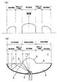
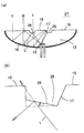
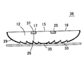
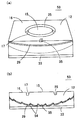
このためLEDチップから斜め方向へ出射された光も効率よく前方へ取り出せるようにすると共に薄くて大面積化の可能な発光光源が従来より提案されている。図1はこのような発光光源1の構造を示す斜視図、図2(a)はその断面図、図2(b)はその正面輝度の分布を示す図であって、この発光光源1は特開2002−94129号公報(特許文献1)に開示されたものである。この発光光源1は、略皿状をした透明なモールド樹脂2内の中心部にLEDチップ3を封止したものであり、モールド樹脂2の背面には凹面鏡状をした反射ミラー4が設けられている。また、モールド樹脂2の前面中央部には凸レンズ状をした直接出射領域5が形成され、その周囲には平面状をした全反射領域6が環状に形成されている。
【0005】
しかして、LEDチップ3に通電してLEDチップ3を発光させると、図2(a)に示すように、LEDチップ3から直接出射領域5に向けて出射された光Lは、凸レンズ状をした直接出射領域5を透過すると共に直接出射領域5を透過する際にレンズ作用を受けて屈折させられ、発光光源1からほぼ真っ直ぐ前方へ向けて出射される。また、LEDチップ3から全反射領域6へ向けて出射された光Lは、全反射領域6の界面において反射ミラー4に向けて全反射され、反射ミラー4で反射された後、全反射領域6を透過して発光光源1からほぼ真っ直ぐ前方へ向けて出射される。
【0006】
このような発光光源1では、全反射領域6の内周部で全反射された光Lは、一旦反射ミラー4へ戻って反射ミラー4で反射され、再び全反射領域6に達して全反射領域6から出射されるので、全反射領域6から反射ミラー4へ向かう間に光Lが全反射領域6の内周部よりも外側へ広がり、全反射領域6の外周部分から出射される。このため、図2(a)に示すように、直接出射領域5と全反射領域6の外周部分とは発光領域となるが、その中間に位置する全反射領域6の内周部は光が出射されないので、発光しない領域となる。
【0007】
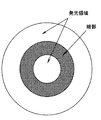
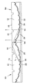
図2(b)は発光光源1を正面から見たときの輝度分布を、発光光源1の中心軸を通る断面内で概略的に表したものであり、図3は発光光源1を正面から見た様子を表している。図2(a)(b)に示すように発光光源1には発光しない領域が生じるので、従来の発光光源1では、正面から見たときに幅の広いリング状をした暗部(暗環)が生じ、均一に面発光させることができなかった。特に、直径が数センチもあるような発光光源では、この暗部がはっきりと見えてしまい、均一に面発光させることができなかった。
【0008】
尚、特開2002−134794号公報(特許文献2)には、直接出射領域の外周部にリング状の反射板をインサートしたり、スリット(空気層)を設けることによって暗部を低減させる方法が開示されているが、このような発光光源ではモールド部の成形工程やその後工程が複雑になり、コストが高くつく問題がある。
【0009】
【発明の開示】
本発明は、上記のような技術的課題に鑑みてなされたものであり、モールド部の背面に反射部材を備えた発光光源において、簡単な構造により正面輝度の均一性をより向上させることを目的としている。
【0010】
本発明にかかる発光光源は、光を反射させる反射部材と、前記反射部材の光反射面側に配置された導光部と、前記導光部に向けて光を出射する発光素子とを備え、前記導光部の表面は、前記発光素子から発した光を透過させて直接外部へ出射する直接出射領域と、前記発光素子から発した光を全反射させ、前記反射部材へ向かわせる前記直接出射領域の周囲に設けられた第1の全反射領域とからなり、前記第1の全反射領域は、前記反射部材で反射した光を外部に出射させる外周部と、前記直接出射領域と前記外周部との間に位置する内周部とからなる発光光源において、前記直接出射領域と前記内周部との間に第2の全反射領域を有し、前記第2の全反射領域は、前記内周部と前記直接出射領域との間で前記導光部の中心軸に対して傾斜し、それにより発光素子から発した光を全反射させて前記直接出射領域へ向かわせ、かつ直接出射領域で全反射させ、前記導光部の中心軸を横切らせ、前記反射部材へ向かわせ、反射部材で反射させ、前記内周部から外部へ出射させることを特徴としている。
【0011】
本発明にかかる発光光源にあっては、発光素子の光を直接出射させる直接出射領域と、発光素子の光を全反射させ、さらに反射部材で反射させて外部へ出射させる第1の全反射領域とは別に、発光素子の光を全反射させ、さらに直接出射領域で全反射させ、さらに反射部材で反射させて外部へ出射させる第2の全反射領域を有しているので、第2の全反射領域の位置や形状等によって導光部から出射される光の分布を制御することができ、発光光源の正面輝度の分布を均一化させることが可能になる。
【0012】
特に、本発明にかかる発光光源の実施態様においては、前記第2の全反射領域は、第2の全反射領域及び前記直接出射領域で全反射された後に前記反射部材で反射された光の少なくとも一部は、前記直接出射領域を透過する光も前記第1の全反射領域及び前記反射部材で反射された光も出射されない前記内周部の領域から出射されるように形状を定められているので、直接出射領域及び第1の全反射領域だけでは暗部となる領域へ光を送り込むことができ、発光光源における暗部を明るくすることによって正面輝度の均一性を向上させることができる。
【0013】
また、本発明にかかる発光光源の別な実施態様は、前記内周部と前記第2の全反射領域との間に第3の全反射領域を有し、前記第3の全反射領域と前記内周部及び前記外周部とは互いに前記発光素子から異なる距離に配置されている。この第3の全反射領域によれば、第3の全反射領域を設ける位置や角度などによって発光素子から発した光の一部を制御することができ、発光光源の正面輝度の分布をより均一化することができる。
【0015】
また、本発明にかかる発光光源のさらに別な実施態様における前記反射部材は、前記第1の全反射領域で全反射された光を反射させる領域と、前記第2の全反射領域及び前記直接出射領域で全反射された光を反射させる領域とに分割されている。このように、反射部材を第1及び第2の全反射領域に対応する領域に分割すれば、各領域を個々に独立して設計することができ、反射部材の設計の自由度が増す。
【0016】
また、本発明にかかる発光光源のさらに別な実施態様では、第3の全反射領域を備えた発光光源における前記反射部材が、前記第1の全反射領域で全反射された光を反射させる領域と、前記第2の全反射領域及び前記直接出射領域で全反射された光を反射させる領域と、前記第3の全反射領域で全反射された光を反射させる領域とに分割されている。このように、反射部材を第1、第2及び第3の全反射領域に対応する領域に分割すれば、各領域を個々に独立して設計することができ、反射部材の設計の自由度が増す。
【0017】
また、本発明にかかる発光光源のさらに別な実施態様における前記反射部材は、前記発光素子から発した光を反射させて当該光を前記導光部の前面から直接外部へ出射させることのできる領域をさらに備えているので、発光素子から大きな出射角度で横方向に出射された光も反射部材で反射させて前面から出射させることができ、光の利用効率を向上させることができる。
【0018】
また、第3の全反射領域を備えた発光光源のさらに別な実施態様においては、前記第1の全反射領域と前記第3の全反射領域とを前記発光素子から異なる距離に配置することによって前記導光部に生じた凹部に、第1の全反射領域と第3の全反射領域のうち少なくとも一方の面と連続した面を形成するようにして導光部と異なる屈折率の光透過性媒質を充填しているので、凹部にゴミやホコリ等が溜まって光を散乱させたり、光を遮ったりするのを防止することができ、発光光源の汚れによって発光光源が劣化するのを防ぐことができる。
【0019】
また、本発明にかかる発光光源のさらに別な実施態様においては、前記導光部の光出射側の面の全体を、導光部と異なる屈折率の光透過性媒質により覆っているので、導光部の表面の凹凸にゴミやホコリ等が溜まって光を散乱させたり、光を遮ったりするのを防止することができ、発光光源の汚れによって発光光源が劣化するのを防ぐことができる。また、光透過性媒質として導光部よりも硬度の高いものを用いれば、導光部を保護することができる。
【0020】
また、本発明にかかる発光光源のさらに別な実施態様においては、前記発光素子と前記導光部との間に、拡散剤又は蛍光体を分散させた光透過領域を形成しているので、発光素子から発しられた光を拡散剤で散乱させたり、蛍光体で二次発光させたりすることができ、擬似的に発光素子を拡大させることができる。
【0021】
また、本発明にかかる発光光源アレイは、本発明にかかる発光光源を複数連結したものであって、隣接する発光光源のうち一方の発光光源から他方の発光光源の導光部内へ漏れた光を他方の発光光源の反射部材で反射させることにより他方の発光光源の光出射側の面から出射させられるように反射部材の形状を定めたことを特徴としている。
【0022】
本発明の発光光源アレイにあっては、一方の発光光源から他方の発光光源へ漏れた光を他方の発光光源の反射部材で反射させて他方の発光光源から出射させることができるので、発光光源から漏れた光を再利用することができ、光の利用効率をより向上させることができる。
【0023】
本発明の照明装置は、本発明にかかる発光光源を複数配列した発光光源アレイと、前記発光光源アレイに電力を供給する電源装置とを備えたことを特徴としている。このような照明装置によれば、軽量で、薄型かつ大面積で、均一な発光面を有する照明装置を得ることができる。しかも、電源装置を備えているので、持ち運ぶことも可能である。
【0024】
本発明の表示装置は、本発明にかかる発光光源を複数配列した発光光源アレイと、前記発光光源アレイを構成する各発光光源の点灯を制御する制御部とを備えたことを特徴としている。このような表示装置によれば、軽量で、薄型かつ大面積で、均一な発光面を有する表示装置を得ることができる。しかも、制御部を備えているので、さまざまな表示を行うことができ、宣伝広告やディスプレイ用、信号機などに最適に使用できる。
【0025】
なお、この発明の以上説明した構成要素は、可能な限り任意に組み合わせることができる。
【0026】
【発明の実施の形態】
(第1の実施形態)
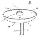
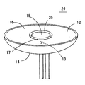
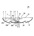
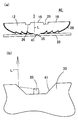
図4は本発明の一実施形態による発光光源11の構造を示す斜視図、図5(a)はその断面図、図5(b)は当該発光光源11の正面における輝度分布を示す図である。この発光光源11にあっては、高屈折率の光透過性材料、例えば透明樹脂によって略皿状をしたモールド部(導光部)12が成形されている。モールド部12を構成する光透過性材料としては、エポキシ樹脂やアクリル樹脂などの光透過性樹脂を用いてもよく、ガラス材料を用いてもよい。LEDチップやランプ等の発光素子13は、一方のリード端子18の先端部に形成されたステムの上にダイボンドされており、発光素子13と他方のリード端子19との間はボンディングワイヤ20によって電気的に接続されている。発光素子13とリード端子18、19の先端部とはモールド部12内に封止されており、発光素子13はモールド部12内の裏面側中心部に位置している。
【0027】
モールド部12の裏面には、モールド部12の前面で全反射された光を前方へ向けて反射させるための凹面鏡状をした反射部材14が設けられている。反射部材14は、モールド部12の裏面に蒸着させられたAu、Ag、Al等の金属被膜でもよく、表面を鏡面加工して表面反射率を高くしたアルミニウム等の金属板でもよく、表面にAu、Ag、Al等のメッキを施した金属や樹脂などの曲面板でもよい。
【0028】
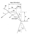
モールド部12の前面中央部には円形(すなわち、真円、楕円など)の直接出射領域15が設けられており、その外側には環状をした全反射領域(第1の全反射領域)16が設けられており、直接出射領域15と全反射領域16との間には傾斜全反射領域(第2の全反射領域)17が設けられている。直接出射領域15はモールド部12の中心軸と垂直な平面によって形成された平滑な円形の領域であり、全反射領域16もモールド部12の中心軸と垂直な平面によって形成された平滑な環状領域である。また、傾斜全反射領域17はモールド部12の前面側へ向かうほど次第に直径が小さくなったテーパー状に形成されており、直接出射領域15及び傾斜全反射領域17は全反射領域16の中央部において前面側へ円錐台状に突出している。
【0029】
しかして、リード端子18、19を通じて発光素子13に通電すると、図5(a)に示すように、発光素子13から直接出射領域15に向けて出射された光Lは、直接出射領域15を透過して発光光源11から直接前方へ出射される。また、発光素子13から全反射領域16へ向けて出射された光Lは、全反射領域16で全反射された後、反射部材14に入射して反射部材14で反射され、全反射領域16の内周部を除く領域から発光光源11の前方へ出射される。さらに、発光素子13から傾斜全反射領域17へ入射した光Lは、傾斜全反射領域17で全反射されて直接出射領域15の周辺部へ入射し、直接出射領域15で全反射された後に反射部材14に入射し、反射部材14で反射されて発光光源11の前方へ出射される。ここで、傾斜全反射領域17、直接出射領域15の周縁部及び反射部材14で3回反射された光Lは、暗部から出射されるように設計されている。なお、本発明に関しては、直接出射領域15と全反射領域16及び反射部材14で2回反射された光を出射させる領域(全反射領域16の外周部)との間にあって、直接出射領域15から直接出射される光も、全反射領域16及び反射部材14で2回反射された光も出射されない領域を暗部というものとする。
【0030】
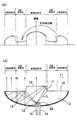
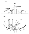
図5(b)は本実施形態による発光光源11と従来例の発光光源1から出射される光の輝度を比較して表した図である。図5(b)において破線で表した強度分布は、図1の発光光源1から出射される光の輝度分布(図2(b)と同じもの)を示している。図5(b)において実線で表した輝度分布は、従来例の直接出射領域5を直接出射領域15及び傾斜全反射領域17に置き換えた(全反射領域6の領域と全反射領域16の領域は一致)本実施形態の発光光源11から出射される光の強度分布を表している。このような場合には、図5(a)の光線図からも分かるように、直接出射領域5の外周部に相当する領域に傾斜全反射領域17を設けることにより、直接出射領域5の外周部から直接出射されていた光の一部を暗部となっていた領域(モールド部12の中心軸を挟んで反対側)へ再分配させて暗部から出射させることができるので、暗部を低減させて発光光源11から出射される光の輝度を均一化することができる。
【0031】
図6(a)は本実施形態による発光光源で傾斜全反射領域17の位置を少し異ならせたものを示しており、図6(b)はその発光光源11と従来例の発光光源1から出射される光の輝度分布を比較して表した図である。図6(b)において破線で表した強度分布は、図1の発光光源1から出射される光の強度分布(図2(b)と同じもの)を示している。図6(b)において実線で表した強度分布は、従来例の全反射領域6の内周部に傾斜全反射領域17を形成し、レンズ状の直接出射領域5を平坦な直接出射領域15に置き換えた本実施形態の発光光源11から出射される光の輝度分布を表している。このような場合には、図6(a)の光線図からも分かるように、全反射領域6の内周部に傾斜全反射領域17を設けることにより、全反射領域16において暗部の外周側から出射されていた光の一部を暗部へ再分配させて暗部から出射させることができるので、発光光源11から出射される光の輝度を均一化することができる。
【0032】
また、傾斜全反射領域17を図5(a)と図6(b)の中間位置に設けた場合には、直接出射領域5の外周部から出射されていた光と全反射領域6の内周部で全反射された後に全反射領域6から出射されていた光とを暗部であった箇所へ導いて出射させることができ、やはり発光光源11から出射される光の輝度を均一化することができる。
【0033】
特開2002−134794号公報(特許文献2)に記載されている発光光源では、直接出射領域の外周部にリング状の反射板をインサートしたり、スリット(空気層)を設けたりしているので、成形工程が複雑になったり、後工程が必要になったりするが、本発明によれば、発光光源のモールド部の正面形状を変えるだけで暗部の輝度を向上させて輝度の均一化を図ることができるので、発光光源の製造が簡単で、コストの上昇も抑えることができる。
【0034】
つぎに、本実施形態において、直接出射領域15に入射した光Lがその界面を透過する条件と、全反射領域16に入射した光がその界面で全反射する条件と、傾斜全反射領域17に入射した光がその界面と直接出射領域15で2度全反射する条件とを求める。図7に示すように、直接出射領域15の外径をD1、傾斜全反射領域17の下端外周の直径をD2(ただし、D2≧D1)、傾斜全反射領域17の下端から上端までの垂直方向における高さをH、傾斜全反射領域17の下端から垂直に計った発光素子13のインサート位置の深さをTとし、モールド部12の軸心を通る断面における傾斜全反射領域17の傾きをαとする。なお、傾斜全反射領域17の傾きα、傾斜全反射領域17の高さH、直接出射領域15の外径D1、全反射領域16の内径D2の間には、
tanα=(D2−D1)/(2H)
すなわち、
D2=D1+2Htanα …(1)
の関係がある。また、モールド部12の屈折率をn1、モールド部12の前面に接する媒質の屈折率をn2とする。この実施形態では、モールド部12の前面は樹脂と空気との界面となっているが、モールド部12の前面は別な樹脂や多層反射膜等との界面であってもよく、その場合には屈折率n2は、モールド部12前面に接している別な樹脂などの媒質の屈折率となる。
【0035】
まず、図7に示す光線L1のように、直接出射領域15に入射した光が直接出射領域15から出射される条件を求める。発光素子13から直接出射領域15の外周端へ出射される光線L1がモールド部12の中心軸(Z軸)となす角度をθ1とすると、
tanθ1=D1/[2(H+T)]
すなわち、
θ1=arctan[D1/2(H+T)] …(2)
となる。この光線L1が全反射されることなく外部へ出射されるためには、界面への入射角θ1が全反射の臨界角θo=arcsin(n2/n1)よりも小さくなければならないから、条件は下記(3)式となる。
arctan[D1/2(H+T)] < θo
すなわち、
D1 < 2(H+T)tanθo …(3)
【0036】
次に、図7に示す光線L2のように、全反射領域16に入射した光が全反射される条件を求める。発光素子13から全反射領域16の内周端へ出射される光線L2がモールド部12の中心軸(Z軸)となす角度をθ2とすると、
tanθ2=D2/(2T)
すなわち、
θ2=arctan[D2/(2T)] …(4)
となる。この光線L2が全反射されるためには、界面への入射角θ2が全反射の臨界角θo以上でなければならないから、条件は下記(5)式となる。
arctan[D2/(2T)] ≧ θo
ここで、上記(1)式を用いると、
D1 ≧ 2(Ttanθo−Htanα) …(5)
となる。
【0037】
また、図7に示す光線L3のように、傾斜全反射領域17の下端に入射した光が傾斜全反射領域17と直接出射領域15で全反射される条件を求める。発光素子13から傾斜全反射領域17の下端へ出射される光線L3がモールド部12の中心軸(Z軸)となす角度は(4)式で表されるθ2と同じであるから、この光線L3の傾斜全反射領域17への入射角度θ3は、傾斜全反射領域17の傾きαを用いて、
θ3=90°−α−θ2=90°−α−arctan[D2/(2T)] …(6)
と表される。この光線L3が傾斜全反射領域17で全反射されるためには、入射角θ3が全反射の臨界角θo以上でなければならないから、前記(1)式を用いれば、傾斜全反射領域17の下端で全反射される条件は下記(7)式となる。
90°−α−arctan[D2/(2T)] ≧ θo
すなわち、
D1 ≦ 2Tcot(α+θo)−2Htanα …(7)
ついで傾斜全反射領域17の下端で全反射された光線L3が直接出射領域15に入射する入射角θ4は、
θ4=2α+θ2=2α+arctan[D2/(2T)] …(8)
と表される。この光線L3が直接出射領域15で全反射されるためには、入射角θ4が全反射の臨界角θo以上でなければならないから、傾斜全反射領域17の下端で全反射された光線L3が直接出射領域15でも全反射される条件は下記の(9)式となる。
2α+arctan[D2/(2T)] ≧ θo
すなわち、
D1 ≧ 2Ttan(θo−2α)−2Htanα …(9)
【0038】
さらに、図7に示す光線L4のように、傾斜全反射領域17の上端に入射した光が傾斜全反射領域17と直接出射領域15で全反射される条件を求める。発光素子13から傾斜全反射領域17の上端へ出射される光線L4がモールド部12の中心軸(Z軸)となす角度は(2)式で表されるθ1と同じであるから、この光L4の傾斜全反射領域17への入射角度θ5は、

90°−α−arctan[D1/2(H+T)] ≧ θo
すなわち、
D1 ≦ 2(H+T)cot(α+θo) …(11)
ついで、傾斜全反射領域17の上端で全反射された光L4が直接出射領域15に入射する入射角θ6は、
θ6=2α+θ1=2α+arctan[D1/2(H+T)] …(12)
と表される。この光が直接出射領域15で全反射されるためには、入射角θ6が全反射の臨界角θo以上でなければならないから、傾斜全反射領域17の上端で全反射された光L3が直接出射領域15でも全反射される条件は下記の(13)式となる。
2α+arctan[D1/2(H+T)] ≧ θo
すなわち、
D1 ≧ 2(H+T)tan(θo−2α) …(13)
【0039】
さらに、傾斜全反射領域17で反射した光が傾斜全反射領域17の対向する面に入射することなく直接出射領域15へ入射する条件を考える。図7に示すように、傾斜全反射領域17の下端で全反射した光線L3が直接出射領域15に入射する点と直接出射領域15の外周端との距離をDxとすると、
Dx = H[tan(θ2+2α)−tanα] …(14)
となる。傾斜全反射領域17で反射された光が直接出射領域15で反射された後、傾斜全反射領域17の対向領域で遮られることなく反射部材14に達するためには、D1/2がこのDxよりも大きければよいので、
D1 ≧ 2H[tan(θ2+2α)−tanα] …(15)
という条件が得られる。
【0040】
加えて、傾斜全反射領域17及び直接出射領域15で全反射された光については、これが暗部(直接出射領域15を透過する光も、全反射領域16及び反射部材14で反射された光も出射されない領域)の全体から出射される必要がある。このための条件については、反射部材14の曲面形状に依存するので、詳細は述べないが、傾斜全反射領域17及び直接出射領域15で全反射した光を、正面(Z軸方向)から見たとき上記暗部と重なる領域において反射部材14に入射させ、全反射領域16と垂直は方向へ反射させる必要がある。
【0041】
もっとも望ましい発光光源11としては、上記(3)式、(5)式、(7)式、(9)式、(11)式、(13)式、(15)式[ただし、(7)式を満たせば(11)式は満足され、(13)式を満たせば(9)式は満足されるので、実質的には、(3)、(5)、(7)、(13)、(15)の5つの式だけを考慮すればよい。]等の条件を満たすことが望ましいが、本発明の目的は暗部に光を送り込んで輝度の均一性を向上させることにあるので、必ずしも上記条件を全て満たしていなくても差し支えない。例えば、実際の設計にあたっては、上記(7)式、(13)式、(15)式に優先順位を定めて設計すればよい。
【0042】
反射部材14の曲面形状については、できるだけ発光光源11の正面から均一に光が出射されるような形状に設計することが望ましい。例えば、発光光源11の正面形状が円形である場合には、次の(16)式で表されるようなコニック面とすることができる。
【数1】
【0043】
また、反射部材14の曲面形状としては、発光光源11の正面形状が略楕円状をしている場合には、次の(17)式で表されるようなバイコニック面とすることができる。
【数2】
【0044】
反射部材14の形状としては、このようなコニック面やバイコニック面に限るものではないが、コニック面やバイコニック面とすれば、発光光源11をより一層均一発光させることが可能になる。
【0045】
(第2の実施形態)
図8(a)は本発明の別な実施形態による発光光源21の構造を示す斜視図、図8(b)はその断面図である。この発光光源21にあっては、直接出射領域15の周辺部には、傾斜全反射領域17で全反射した光Lを再度全反射させるための平坦面22が形成されており、直接出射領域15の周辺部を除く領域にはレンズ面23が形成されている。
【0046】
図4の実施形態では、直接出射領域15が平坦面となっていたので、直接出射領域15のうち中心部以外の領域から出射される光Lは中心軸から傾いた斜め方向へ出射される。そのため、この実施形態による発光光源21では、傾斜全反射領域17で全反射された光Lを再度全反射させるために必要な領域は平坦面22とし、そのような働きを要求されない領域では直接出射領域15に凸レンズ状又はフレネルレンズ状をしたレンズ面23を形成し、レンズ面23から直接に出射される光Lは、中心軸と平行な方向に揃えて前方へ出射させられるようにしている。よって、この実施形態によれば、斜めに出射される光を低減させ、光の利用効率を向上させることができる。
【0047】
図9は理論上必要とされる平坦面22の最小幅Dxを計算するための参考図である。発光素子13から傾斜全反射領域17の下端へ向けて出射される光Lの出射角をθ2とし、傾斜全反射領域17の傾きをα、傾斜全反射領域17の高さをHとすれば、環状に形成された平坦面22の幅Dxは図9から次のように求められる。なお、このDxは(14)式と同じものである。
Dx = H[tan(θ2+2α)−tanα] …(18)
【0048】
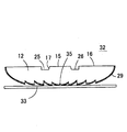
(第3の実施形態)
図10は本発明のさらに別な実施形態による発光光源24の構造を示す斜視図、図11(a)はその断面図、図11(b)は当該発光光源24の正面における輝度分布を示す図である。この発光光源24にあっては、円形状をした平坦な直接出射領域15とその外側に形成された平坦な全反射領域16との間に円環状をした溝25を形成し、溝25の底面に全反射面(第3の全反射領域)26を形成すると共にその内周側側壁面を傾斜させて傾斜全反射領域17を形成している。図示例では、直接出射領域15と全反射領域16とは同一平面内に形成されており、直接出射領域15は全反射領域16と同じ高さに位置しているが、直接出射領域15を溝25内で全反射領域16よりも突出させて直接出射領域15を全反射領域16よりも高くしてあっても差し支えない。また、上記溝25は直接出射領域15と全反射領域16との間に設ければよいが、特に図12(a)に示すように、発光素子13から全反射の臨界角θoと等しい出射角で出射された光が全反射面26の内周側の縁に達するように溝25を配置するのが望ましい。
【0049】
しかして、この発光光源24によれば、図11(a)(b)に示すように、直接出射領域15の外周に位置する傾斜全反射領域17へ入射した光は、傾斜全反射領域17及び直接出射領域15で2回全反射された後、反射部材14により前方へ向けて出射され、直接出射領域15からの直接出射光や全反射領域16及び反射部材14で反射した2回反射光が届かない暗部へ出射される。これは第1の実施形態と同じ作用によるものである。
【0050】
さらに、この発光光源24によれば、図11(a)に破線で示す光Lのように溝25が設けられていなければ全反射領域16で全反射された後に反射部材14に入射する光が、全反射面26で全反射することによって発光素子13側へシフトさせられる。この結果、図11(b)に示すように、溝25を設ける前には暗部に隣接する箇所から出射されていた光が、溝25を設けることによって暗部内へシフトした位置から出射されることになり、発光光源24から出射される光の輝度がより一層均一化する。
【0051】
図12(b)は溝25の深さδと光線のシフト量との関係を示す図である。全反射領域16から計った溝25の深さをδ、全反射領域16から垂直に計った発光素子13のインサート位置の深さをTとし、発光素子13から出射角θ7(≧θo)で出射された光Lを考える。溝25が無くて全反射領域16で全反射される光Lが発光素子13の配置されている水平面を通過する位置を発光素子13からK2の距離の点であるとすると、K2は次式で表される。
K2=2Ttanθ7 …(19)
また、溝25の底面に位置する全反射面26で全反射された光Lが発光素子13の配置されている水平面を通過する位置を発光素子13からK1の距離の点であるとすると、K1は次式で表される。
K1=2(T−δ)tanθ7 …(20)
よって、(19)式、(20)式よりシフト量K2−K1が次のように求まる。
K2−K1=2δtanθ7 …(21)
これより、溝25の深さδによって全反射面26で全反射される光のシフト量D2−D1を調整し、その光Lの出射位置を制御できることが分かる。
【0052】
(第4の実施形態)
図13(a)は本発明のさらに別な実施形態による発光光源27の構造を示す断面図、図13(b)はその溝25の近傍を示す拡大断面図である。この発光光源27は、図13(b)に示すように、図10の発光光源24において、溝25の底面に設けられた全反射面26をβだけ傾斜させたものである。このように全反射面26の底面を傾けることにより、発光素子13から全反射の臨界角θoよりも小さな出射角で出射された光も全反射面26で全反射させて暗部へ送り出すことができるので、溝25の幅を広くして暗部へ送り出す光量を増加させることができ、輝度をより一層均一化させることができる。あるいは、溝25の位置を直接出射領域15の側へ寄せることにより、直接出射領域15の縁から大きな角度で斜め方向へ出射されている光を暗部へ送り出すことができ、光の利用効率を向上させることができる。更に、全反射面26の傾きβを設計パラメータとすることができるので、光線の挙動(光路)の制御が容易になる。
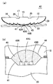
【0053】
図14は傾斜全反射領域17や全反射面26等の光学配置を決めるための条件を求めるための参考図である。図14に示すように、直接出射領域15の外径をD1、傾斜全反射領域17の下端から上端までの垂直方向における高さをH、傾斜全反射領域17の下端から垂直に計った発光素子13のインサート位置の深さをTとし、モールド部12の軸心を通る断面における傾斜全反射領域17の傾きをαとする。なお、図14では、一般化するために傾斜全反射領域17の高さHを溝25の深さδよりも大きくしているが、図13の図示例では、直接出射領域15と全反射領域16とが同一面となっているので、この場合には、傾斜全反射領域17の高さHと溝25の深さδとは等しくなる。
【0054】
上記のようにT、H、α等を定義すれば、発光素子13から出射された光が傾斜全反射領域17で全反射される条件は、発光素子13から傾斜全反射領域17の下端へ出射される光の出射角をθ2とすれば、
90°−θ2−α ≧ θo
となるから(θoは全反射の臨界角)、第1の実施形態の(7)式と同様、次のように表される。
D1 ≦ 2Tcot(α+θo)−2Htanα …(22)
【0055】
また、傾斜全反射領域17で全反射された光が直接出射領域15で全反射される条件は、第1の実施形態の(13)式及び(15)式と同様、
D1 ≧ 2(H+T)tan(θo−2α) …(23)
D1 ≧ 2H[tan(θ2+2α)−tanα] …(24)
と表される。
【0056】
さらに、全反射面26の内周側の端に入射する光の入射角はθ2+βであるから、全反射面26に入射した光が全反射面26で全反射される条件としては、θ2+βが全反射の臨界角θoよりも大きければよい。すなわち、
β ≧ θo−θ2 …(25)
の条件を満たせばよい。
【0057】
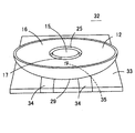
(第5の実施形態)
図15は本発明のさらに別な実施形態による発光光源28の裏面側からの斜視図、図16はその断面図である。この発光光源28において、モールド部12の裏面に形成されている反射部材29は、環状をした複数の反射領域29a、29b、…によって構成されており、フレネル反射面を構成している。このように反射部材29をフレネル反射面状に形成すれば、発光光源28をより薄型化することが可能になる。また、複数の各反射領域29a、29b、…を互いに独立したパラメータで設計することにより、各領域を最適設計することができ、より均一に発光させることが可能になる。
【0058】
(第6の実施形態)
図17は本発明のさらに別な実施形態による発光光源30の断面図である。この発光光源28において、モールド部12の前面において直接出射領域15と全反射領域16の間に溝25を形成し、溝25の底面に全反射面26を構成している。また、モールド部12の裏面に形成されている反射部材31は、環状をした4つの反射領域31a、31b、31c、31dによって構成されており、フレネル反射面を構成している。ここで、反射領域31dは、発光素子13から出射されて全反射領域16で全反射された光を受けて全反射領域16から前方へ向けて出射させるような形状及び配置となっている。反射領域31cは、発光素子13から出射されて全反射面26で全反射された光を受けて全反射領域16から前方へ向けて出射させるような形状及び配置となっている。反射領域31bは、発光素子13から出射されて傾斜全反射領域17及び直接出射領域15で全反射された光を受けてモールド部12の前面から前方へ向けて出射させるような形状及び配置となっている。反射領域31aは、発光素子13から直接反射面31に入射するような大きな出射角方向へ出射された光を受けてモールド部12の前面から前方へ向けて出射させるような形状及び配置となっている。
【0059】
この実施形態によれば、入射する光の光路の特性に応じて反射領域31a、31b、31c、31dを分け、各特性に応じて反射領域31a、31b、31c、31dを設計することができるので、光源装置をより一層均一に発光させることが可能になる。
【0060】
(第7の実施形態)
図18は本発明のさらに別な実施形態による発光光源32の斜視図、図19はその断面図である。この発光光源32はリード端子を設けない表面実装型のものである。背面に反射部材29を形成されたモールド部12は支持基板33の上に取り付けられている。支持基板33は放熱板を兼ねており、熱伝導率の高い金属板やアルミナ等のセラミック板によって形成されている。支持基板33には、面から裏面にかけて(支持基板33が金属製である場合には、絶縁膜層を介して)帯状をした一対の電極膜34が形成されており、支持基板33の上にLEDチップ等の発光素子を樹脂モールドした発光素子35を搭載し、両電極膜34と発光素子35とを電気的に接続している。支持基板33の上面に固定されたモールド部12の中央部下面には凹部が形成されており、支持基板33の上面に設けられた発光素子35は当該凹部内に納められている。
【0061】
なお、図18及び図19の図示例では、直接出射領域15と全反射領域16との間に溝25を形成しているが、第1の実施形態のように全反射領域16から円錐台状をした直接出射領域15及び傾斜全反射領域17が突出した形状となっていてもよい。また、反射部材29もフレネル反射面状のものを用いているが、第1の実施形態のように全体が滑らかな形状をした反射部材14を用いてもよい。
【0062】
この実施形態にあっては、リード端子を用いることなく支持基板33の上に発光素子35とモールド部12を実装して表面実装型にしているので、発光光源32を非常に薄くすることが可能になる。また、支持基板33は放熱機能を備えているので、大面積の放熱板を備えた発光光源32となり、大電力用の発光素子35を用いたり、複数個の発光素子35を実装したりして大面積で明るい発光光源32を得ることができる。
【0063】
(第8の実施形態)
図20は本発明のさらに別な実施形態による発光光源36の斜視図、図21はその断面図である。この発光光源36においては、モールド部12の前面に設けられた環状の溝25をモールド部12よりも屈折率の低い光透過性材料、例えば透明樹脂からなる充填部37によって埋め、モールド部12の前面が平坦な面となるようにしている。モールド部12の前面に溝25が設けられていると、溝25内にゴミやホコリが溜まり、その部分の輝度が落ちて暗くなったり、散乱により指向特性が悪くなる恐れがある。この実施形態のように、溝25を充填部37で埋めることにより、溝25にゴミやホコリが溜まるのを防ぐことができるので、ゴミやホコリで発光光源36の輝度が部分的に低下して暗くなったり、指向特性が低下したりするのを防止することができる。
【0064】
(第9の実施形態)
図22は本発明のさらに別な実施形態による発光光源38の斜視図、図23はその断面図である。この発光光源38においては、モールド部12の前面の全体を屈折率の低い光透過性材料、例えば透明樹脂からなる被覆部39で覆い、同時に、環状の溝25も被覆部39によって埋めている。この実施形態によれば、モールド部12の前面を被覆部39で覆っているので、例えば被覆部39の材料としてモールド部12よりも硬度の高い材料を用いれば、モールド部12を保護してモールド部12に傷がつくのを防止することができる。また、溝25を被覆部39で埋めることにより、溝25にゴミやホコリが溜まるのを防ぐことができ、ゴミやホコリで発光光源36の輝度が部分的に低下して暗くなったり、指向特性が低下したりするのを防止することができる。
【0065】
(第10の実施形態)
図24(a)は本発明のさらに別な実施形態による発光光源40の断面図、図24(b)はその一部拡大した断面図である。この実施形態にあっては、支持基板33の上面にテーパー状、パラボラ状などの形状をした凹所41を設け、凹所41の表面を鏡面加工又は鏡面処理している。発光素子35は凹所41内の中央部に実装されている。このような構造の発光光源40によれば、発光素子35から大きな出射角度で出射された光は、凹所41の外周面で反射することによって前方へ偏向され、直接出射領域15を透過して前方へ出射される。このような実施形態によれば、支持基板33に設けた凹所41によって大きな出射角度で発光素子35から出射された光を制御することができるので、光の利用効率を向上させることができると共に設計の自由度も向上する。
【0066】
(第11の実施形態)
図25(a)は本発明のさらに別な実施形態による発光光源42の断面図、図25(b)はその一部拡大した断面図である。この実施形態にあっては、支持基板33の上面に設けられた凹所41内に赤色LED等の発光素子43R、緑色LED等の発光素子43G、青色LED等の発光素子43Bをそれぞれ少なくとも1個ずつ搭載し、モールド部12の中央部下面に設けられた凹部44と凹所41の間の空間に、微細な金属粉末や金属フィラメント等の拡散剤を分散させられた光透過性材料45を充填している。
【0067】
このような発光光源42によれば、例えば赤色発光素子43R、緑色発光素子43G及び青色発光素子43Bを同じパワーで発光させると、各発光素子43R、43G、43Bから出射された赤色光、緑色光及び青色光は光透過性材料45内の拡散剤によって散乱され、互いに混色されて白色光となり、発光光源42が白色発光する。また、例えば赤色発光素子43Rだけを発光させれば、発光光源42は赤色発光する。よって、この発光光源42によれば、発光させる発光素子43R、43G、43Bと各パワーを変化させることにより、フルカラー表示させることができ、しかも異なる色の発光素子を発光させる場合でも拡散剤によって効果的に混色させることができるので、1つの発光素子とみなすことができる。また、この発光光源42は光透過性材料45の表面(凹部44との界面)を発光面とみなすことができる。さらに、この発光光源42では、放熱機能を有する支持基板33を用いているので、各発光素子43R、43G、43Bのパワーを稼ぐことができる。なお、ここでは赤、緑、青の発光素子を内蔵した場合について説明したが、同じ発光色の発光素子を複数個内蔵させた場合でも、1つの発光素子のように発光させることができ、大きな輝度の発光光源42を得ることができる。また、1つの発光素子とみなして設計できるので、発光光源42の設計が容易になる。
【0068】
(第12の実施形態)
図26(a)は本発明のさらに別な実施形態による発光光源46の断面図、図26(b)はその一部拡大した断面図である。この実施形態にあっては、支持基板33の上面に設けられた凹所41内に青色発光の発光素子を用いた発光素子47を1個又は複数個搭載し、モールド部12の中央部下面に設けられた凹部44と凹所41の間の空間に蛍光体を分散させられた光透過性材料48を充填している。
【0069】
このような発光光源46によれば、発光素子47を発光させると、発光素子47から出射された青色光によって光透過性材料48内の蛍光体が発光し、光透過性材料48全体が白色発光する。よって、複数の発光素子47が用いられていても1つの発光素子とみなして設計することができ、発光光源46の設計が容易になる。
【0070】
また、発光素子47として紫外線発光の発光素子を用い、光透過性材料48内には赤色蛍光体、緑色蛍光体及び青色蛍光体を均一に分散させておいてもよい。このような構成でも、発光素子47から出射された紫外線光によって赤色蛍光体、緑色蛍光体及び青色蛍光体が発光させられるので、発光光源46を白色発光させることができる。
【0071】
(第13の実施形態)
図27は本発明にかかる発光光源の種々の正面形状を示す図である。上記実施形態では、正面形状が円形(すなわち、真円形又は楕円形)の発光光源を説明したが、発光光源の正面形状は円形に限るものではない。図27(a)に示す発光光源49は、1点鎖線で示す真円形の発光素子49aを設計した後、周囲の六ヶ所をカットして正六角形に整形したものである。図27(b)に示す発光光源50は、1点鎖線で示す真円形の発光素子50aを設計した後、周囲の四ヶ所をカットして正方形に整形したものである。図27(c)に示す発光光源51は、1点鎖線で示す真円形の発光素子51aを設計した後、周囲の四ヶ所をカットして長方形に整形したものである。図27(d)に示す発光光源52は、1点鎖線で示す楕円形の発光素子52aを設計した後、周囲の四ヶ所をカットして長方形に整形したものである。なお、周囲をカットするのは、設計上の順序としてカットするものであって、実際の製造工程でカットするものではない。
【0072】
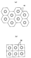
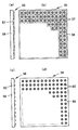
これらの発光光源49、50、51、52等を用いれば、線状又は面上に並べたとき、円形の発光光源のように発光光源どうしの間に隙間が生じることが無く、互いに密着させて配列させることができる。例えば、図28(a)は六角形の発光光源49を隙間無く面状に配列した様子を表している。また、図28(b)及び図29(a)はいずれも長方形又は正方形の発光光源50を隙間無く面状に配列させた様子を表している。図28(b)では、発光光源50を縦横に整然と配列させているので、発光光源50のコーナー(発光光源50の中心からもっと遠いので最も輝度が低い)が1カ所に集中しており、この箇所で暗くなる恐れがあるが、図29(a)のように隣り合う列の発光光源50どうしで半ピッチずつずらすようにすればコーナー部が1カ所に集中するのを避けることができ、局所的に暗くなるのを緩和することができる。図29(b)では、正方形又は長方形の発光光源52を横一列に並べた様子を表している。従って、図28(a)(b)及び図29(a)のような配列によれば大面積の面光源を得ることができ、図29(b)のような配列によれば一方向に長い線状光源を得ることができる。
【0073】
(第14の実施形態)
図30(a)は本発明のさらに別な実施形態による発光光源53の構造を示す斜視図、図30(b)はその断面図である。この発光光源53にあっては、支持基板33の上に発光素子35とフレネル型の反射板形状をした反射部材29を配置し、反射部材29の内部及び反射部材29と支持基板33の空間にモールド部12を成形し、モールド部12の前面に直接出射領域15や全反射領域16、溝25等を形成している。また、反射部材29は、その各環状領域の間の段差部分54でも不連続となることなく光反射面を構成しており、しかも、その段差部分54は、垂直面となっておらず、各環状領域と反対向きに傾斜した傾斜面となっている。さらに、この発光光源53は、設計上において円形の発光光源の四ヶ所をカットすることにより正方形ないし長方形状に形成されている(図27(b)(c)(d)参照)。
【0074】
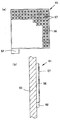
円形の発光光源では、その外周面は反射部材によって囲まれているので、発光光源から真横に光が出射されることはないが、発光光源の周囲をカットして多角形状、例えば正方形や長方形にすると、図30(a)に示す発光光源53のように、モールド部12の正面と反射部材29の縁との間に隙間が生じる。そのため、全反射領域16で全反射された光が、この側面の隙間から漏れてしまい、光のロスによって光利用効率が低下する。
【0075】
図31は図30(a)(b)の発光光源53を複数個配列した状態を説明する断面図である。複数個の発光光源53を線状ないし面状に配列していると、図31に示すように、全反射領域16で全反射されて発光光源53の側面の隙間から漏れた光Lは、隣接する発光光源53の内部に侵入する。反射部材29に設けられた傾斜した段差部分54は、側面の隙間から侵入した光Lを前方へ向けて反射させるように設計されている。よって、発光光源53の側面の隙間から漏れた光Lが隣接する発光光源53へ侵入すると、傾斜した段差部分54で反射され、隣接する発光光源53から正面へ向けて出射される。よって、この実施形態の発光光源53にあっては、隙間無く配列させることが可能になると共に光のロスを低減させて光利用効率を向上させることができる。
【0076】
図32(a)(b)は、本発明にかかる正方形又は長方形の発光光源57(例えば、図30(a)(b)のような発光光源53)を基板56の表面全体に隙間無く並べた光源装置55の側面図及び正面図である。個々の発光光源57は比較的大きな発光面積を有し、しかも均一に発光させることができるので、このような発光光源57を隙間無く配列させることにより、全体としてムラ無く均一に発光させることができる大面積の光源装置55を得ることができる。
【0077】
図32(c)(d)は、従来の発光光源60(例えば、砲弾型のLED)を同じピッチで基板59の全面に配列させた光源装置58の側面図及び正面図を表している。このような光源装置58では、個々の発光光源60が目立ってつぶつぶ感があり、かなりの輝度ムラがある。これに対し、図32(a)(b)の光源装置55では、輝度ムラのない均一面発光が可能になる。
【0078】
(第15の実施形態)
図33(a)は本発明にかかる発光光源の応用例を示す正面図であって、図32(a)(b)に示した光源装置55にバッテリー等の電源装置62を付加した照明装置61である。このような照明装置61によれば、均一発光が可能な薄型、大面積の照明装置61を得ることができ、図33(b)に示すように、壁63や柱に掛けて用いたり、壁63や柱に埋め込んだりして用いることができる。また、軽量であるので、持ち運びも容易に行える。
【0079】
(第16の実施形態)
図34(a)は本発明にかかる発光光源を用いた表示装置64を示す正面図であって、図32(a)(b)に示した光源装置55に制御部及び電源部65を付加したものである。各発光光源57の発光素子35には、赤色LED等の赤色発光素子、緑色LED等の緑色発光素子及び青色LED等の青色発光素子を内蔵したものが用いられている。制御部及び電源部65から各発光光源57には、発光色と発光強度を制御する信号が送られ、それによって所望のフルカラー表示が行われ、また、表示が変化させられる。このような表示装置64によれば、輝度が高く、フルカラーでムラのない均一面発光が可能になり、見やすいディスプレイを提供することができる。
【0080】
この表示装置64は室内の壁や建物の外壁などに掛けて用いることもできるが、図34(b)に示すようにスタンド66の上に取り付けて自立型の表示装置とすることもできる。
【0081】
(第17の実施形態)
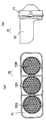
図35(a)は車両への応用を示す一部破断した斜視図である。ハイマウントストップランプ68は、図35(b)に示すように、本発明にかかる発光光源57を一列に並べたものであり、車両67のリアウィンドウの内側に装備されている。また、車両67の後尾に設けられているテールランプ69も、図35(c)に示すように、本発明にかかる発光光源57を2次元状に配列したものである。なお、発光光源57としては、図27(a)に示したような六角形状のものを用いてもよい。
【0082】
(第18の実施形態)
図36(a)は信号機本体71の正面図、図36(b)は信号機本体71の全面に庇状をした遮光カバー73を取り付けた信号機70の側面図である。この信号機本体71には、図36(a)に示すように、緑色に発光する緑色ランプ72G、黄色に発光する黄色ランプ72Y、赤色に発光する赤色ランプ72Rが設けられている。図37は、緑色ランプ72G、黄色ランプ72Yまたは赤色ランプ72Rの構造を示す概略断面図である。各ランプ72G、72Y、72Rは、全面が開口したケース74内に回路基板78に実装された光源装置を納め、その前面を透明ないし着色半透明のカバー75で覆ったものであり、光源装置においては基板76の前面に、それぞれ緑色発光、黄色発光、赤色発光の本発明にかかる発光光源77を隙間無く配列している。
【0083】
なお、信号機70は、一般に高所に設置されるので、地上から見やすいよう、光の出射方向は斜め下方を向いていることが望ましい。そのためには、回路基板78を斜め下方へ向けて傾けてもよく、発光光源46上で各発光光源77を傾けておいてもよい。
【0084】
【発明の効果】
上記のように、本発明の発光光源によれば、第2の全反射領域を設けることにより、その位置や形状等によって導光部から出射される光の分布を制御することができるので、発光光源の正面輝度の分布を均一化させることが可能になる。
【図面の簡単な説明】
【図1】従来例による発光光源の構造を示す斜視図である。
【図2】(a)は同上の発光光源の構造を示す断面図、(b)はその正面輝度の分布を示す図である。
【図3】点灯している同上の光光源を正面から見た様子を表した図である。
【図4】本発明の一実施形態による発光光源の構造を示す斜視図である。
【図5】(a)は同上の発光光源の断面図、(b)は当該発光光源の正面における輝度分布を示す図である。
【図6】(a)は傾斜全反射領域の位置を少し異ならせた発光光源の断面図、(b)はその発光光源と従来例の発光光源から出射される光の輝度分布とを比較して表した図である。
【図7】図5の発光光源における各部分の配置の条件を説明するための図である。
【図8】(a)は本発明の別な実施形態による発光光源の構造を示す斜視図、(b)はその断面図である。
【図9】同上の発光光源において、理論上必要とされる平坦面の最小幅Dxを計算するための図である。
【図10】本発明のさらに別な実施形態による発光光源の構造を示す斜視図である。
【図11】(a)は同上の発光光源の断面図、(b)はその発光光源の正面における輝度分布を示す図である。
【図12】(a)は同上の発光光源における溝の位置を説明するための図、(b)は溝の底の全反射面で全反射されることによる光線のシフト量を求めるための説明図である。
【図13】(a)は本発明のさらに別な実施形態による発光光源の構造を示す断面図、(b)はその溝の近傍を示す拡大断面図である。
【図14】同上の発光光源において、傾斜全反射領域や全反射面等の光学配置を決めるための条件を求めるための図である。
【図15】本発明のさらに別な実施形態による発光光源の裏面側からの斜視図である。
【図16】同上の発光光源の断面図である。
【図17】本発明のさらに別な実施形態による発光光源の断面図である。
【図18】本発明のさらに別な実施形態による発光光源の斜視図である。
【図19】同上の発光光源の断面図である。
【図20】本発明のさらに別な実施形態による発光光源の斜視図である。
【図21】同上の発光光源の断面図である。
【図22】本発明のさらに別な実施形態による発光光源の斜視図である。
【図23】同上の発光光源の断面図である。
【図24】(a)は本発明のさらに別な実施形態による発光光源の断面図、(b)はその一部拡大した断面図である。
【図25】(a)は本発明のさらに別な実施形態による発光光源の断面図、(b)はその一部拡大した断面図である。
【図26】(a)は本発明のさらに別な実施形態による発光光源の断面図、(b)はその一部拡大した断面図である。
【図27】(a)、(b)、(c)及び(d)は、本発明にかかる発光光源の種々の正面形状を示す図である。
【図28】(a)は六角形の発光光源を隙間無く面状に配列した様子を表した図、(b)長方形又は正方形の発光光源を隙間無く面状に配列させた様子を表した図である。
【図29】(a)は長方形又は正方形の発光光源を隙間無く面状に配列させた様子を表した図、(b)は正方形又は長方形の発光光源を横一列に並べた様子を表した図である。
【図30】(a)は本発明のさらに別な実施形態による発光光源の構造を示す斜視図、(b)はその断面図である。
【図31】同上の発光光源を複数個配列した状態の断面図である。
【図32】(a)、(b)は本発明にかかる正方形又は長方形の発光光源を基板の表面全体に隙間無く並べた光源装置の側面図及び正面図であり、(c)、(d)は従来の発光光源を同じピッチで基板の全面に配列させた光源装置の側面図及び正面図である。
【図33】(a)は本発明にかかる照明装置の正面図、(b)はこの照明装置を壁に掛けた状態を示す側面図である。
【図34】(a)は本発明にかかる表示装置を示す正面図、(b)はスタンドの上に取り付けた当該表示装置の斜視図である。
【図35】(a)は本発明にかかるハイマウントストップランプとテールランプを装備した車両の一部破断した斜視図、(b)は車両に設けられたハイマウントストップランプの概略正面図、(c)は車両に設けられたテールランプの概略正面図である。
【図36】(a)は信号機本体の正面図、(b)は信号機の側面図である。
【図37】緑色ランプ、黄色ランプまたは赤色ランプの構造を示す概略断面図である。
【符号の説明】
12 モールド部
13 発光素子
14 反射部材
15 直接出射領域
16 全反射領域
17 傾斜全反射領域
25 溝
26 全反射面
29 反射部材
29a、29b、… 反射領域
31 反射部材
31a、31b、31c、31d 反射領域
33 支持基板
34 電極膜
35 発光素子
43B 発光素子
43G 発光素子
43R 発光素子[0001]
BACKGROUND OF THE INVENTION
The present invention relates to a light emission source, a light emission source array, and a device using the light emission source. In particular, the present invention relates to a light emitting light source or a light emitting light source array using an LED (light emitting diode) chip or the like, an illumination device using the light emitting light source, a display device, or the like.
[0002]
[Background]
[Patent Document 1]
JP 2002-94129 A
[Patent Document 2]
JP 2002-134794 A
[0003]
As a small light-emitting light source, a bullet-type LED in which an LED chip is sealed in a transparent mold resin is well known. In such a light emitting light source, the light emitted forward from the LED chip passes through the interface of the mold resin as it is and directly emitted from the light emitting light source, but the light emitted from the LED chip in the oblique direction is molded resin. It is totally reflected at the interface or scattered on the inner surface of the case, resulting in a loss, and the light utilization efficiency is lowered. Moreover, it is difficult to increase the area of such a light emitting light source.
[0004]
For this reason, there has been conventionally proposed a light-emitting light source that can efficiently extract light emitted in an oblique direction from the LED chip forward and that can be thin and have a large area. FIG. 1 is a perspective view showing the structure of such a
[0005]
When the
[0006]
In such a light
[0007]
FIG. 2B schematically shows the luminance distribution when the light emitting
[0008]
Japanese Patent Laid-Open No. 2002-134794 (Patent Document 2) discloses a method of reducing a dark part by inserting a ring-shaped reflecting plate or providing a slit (air layer) on the outer periphery of a direct emission region. However, in such a light emitting light source, there is a problem that the molding process of the mold part and the subsequent process become complicated and the cost is high.
[0009]
DISCLOSURE OF THE INVENTION
The present invention has been made in view of the technical problems as described above, and aims to further improve the uniformity of front luminance with a simple structure in a light-emitting light source including a reflective member on the back surface of a mold part. It is said.
[0010]
The present inventionDepartureThe light source includes a reflection member that reflects light, a light guide unit disposed on a light reflection surface side of the reflection member, and a light emitting element that emits light toward the light guide unit.The surface of the light guide unit transmits the light emitted from the light emitting element and directly emits the light to the outside, and directly reflects the light emitted from the light emitting element toward the reflecting member. A first total reflection region provided around the emission region, wherein the first total reflection region includes an outer peripheral portion for emitting the light reflected by the reflection member to the outside, the direct emission region, and the outer periphery. Consisting of an inner periphery located betweenIn the light source,A second total reflection region is provided between the direct emission region and the inner peripheral portion, and the second total reflection region is formed between the inner peripheral portion and the direct output region. Inclined with respect to the central axis, whereby the light emitted from the light emitting element is totally reflected and directed to the direct emission region, and is totally reflected at the direct emission region, traversing the central axis of the light guide unit, Direct toward the reflecting member, reflect on the reflecting member, and exit from the inner periphery to the outsideIt is characterized by that.
[0011]
The present inventionDepartureIn the light source, the light from the light emitting element is directly emitted.Direct emission areaThen, the light from the light emitting element is totally reflected, and further reflected by the reflecting member to be emitted to the outside.First total reflection areaApart from that, the light of the light emitting element is totally reflected,Direct emission areaReflect the light with a reflective member and emit it to the outside.Second total reflection areaSo thatSecond total reflection areaThe distribution of light emitted from the light guide unit can be controlled by the position, shape, and the like, and the front luminance distribution of the light emitting light source can be made uniform.
[0012]
In particular, the present inventionDepartureIn the embodiment of the light source,The second total reflection area includes a second total reflection area and the direct emission area.At least part of the light reflected by the reflecting member after being totally reflected byDirect emission areaThe light passing throughFirst total reflection areaAnd the light reflected by the reflecting member is not emitted.Of the inner circumferenceSince the shape is determined to be emitted from the area,Direct emission area and first total reflection areaIt is possible to send light to a region that becomes a dark part, and to improve the uniformity of the front luminance by brightening the dark part in the light emitting light source.
[0013]
Also, the present inventionDepartureAnother embodiment of the light sourceHas a third total reflection region between the inner peripheral portion and the second total reflection region, and the third total reflection region, the inner peripheral portion, and the outer peripheral portion areThe light emitting elements are disposed at different distances from each other. thisThird total reflection areaAccording toThird total reflection areaA part of the light emitted from the light emitting element can be controlled by the position and angle of the light emitting element, and the front luminance distribution of the light emitting light source can be made more uniform.
[0015]
Also, the present inventionDepartureIn another embodiment of the light source, the reflecting member isThe first total reflection areaA region that reflects the light totally reflected byThe second total reflection area and the direct emission areaIt is divided into regions that reflect the light totally reflected at. In this way, the reflective memberFirst and second total reflection regionsIf the region is divided into regions corresponding to, each region can be designed independently and the degree of freedom in designing the reflecting member is increased.
[0016]
Also, the present inventionDepartureIn yet another embodiment of the light source,Third total reflection areaThe reflective member in a light emitting light source comprising:The first total reflection areaA region that reflects the light totally reflected byThe second total reflection area and the direct emission areaA region that reflects the light totally reflected byThe third total reflection regionIt is divided into regions that reflect the light totally reflected at. In this way, the reflective memberFirst, second and third total reflection areasIf the region is divided into regions corresponding to, each region can be designed independently and the degree of freedom in designing the reflecting member is increased.
[0017]
Also, the present inventionDepartureSince the reflection member in still another embodiment of the light source further includes a region that can reflect the light emitted from the light emitting element and emit the light directly from the front surface of the light guide unit to the outside. The light emitted from the light emitting element in the lateral direction at a large emission angle can also be reflected by the reflecting member and emitted from the front surface, and the light utilization efficiency can be improved.
[0018]
Also,With a third total reflection areaIn yet another embodiment of the luminescent light source,The first total reflection region and the third total reflection regionIn the concave portion generated in the light guide portion by disposing at a different distance from the light emitting element,First total reflection region and third total reflection regionSince it is filled with a light-transmitting medium having a refractive index different from that of the light guide portion so as to form a surface continuous with at least one of the surfaces, dust or dust accumulates in the concave portion to scatter light, It can prevent light from being blocked, and it can prevent the light source from deteriorating due to contamination of the light source.it can.
[0019]
Also according to the present inventionStill another source of light emissionIn the embodiment, since the entire light emitting side surface of the light guide unit is covered with a light-transmitting medium having a refractive index different from that of the light guide unit, dust, dust, or the like is formed on the unevenness of the surface of the light guide unit. It can be prevented that the light is accumulated and scattered or blocked, and the light emitting source can be prevented from being deteriorated due to contamination of the light emitting source. Moreover, if a light transmissive medium having a higher hardness than the light guide is used, the light guide can be protected.
[0020]
Also according to the present inventionMore of the light sourceIn another embodiment, since a light transmission region in which a diffusing agent or a phosphor is dispersed is formed between the light emitting element and the light guide portion, the light emitted from the light emitting element is diffused with the diffusing agent. Scattering or secondary light emission with a phosphor can be performed, and the light emitting element can be enlarged in a pseudo manner.
[0021]
The light emitting light source array according to the present invention is also related to the present invention.DepartureA plurality of light sources connected together, and the light emitted from one of the adjacent light sources to the light guide of the other light source is reflected by the reflecting member of the other light source to emit the other light. It is characterized in that the shape of the reflecting member is determined so as to be emitted from the light emitting side surface of the light source.
[0022]
In the light emitting light source array of the present invention, light leaking from one light emitting light source to the other light emitting light source can be reflected by the reflecting member of the other light emitting light source and emitted from the other light emitting light source. The light leaked from the light can be reused, and the light use efficiency can be further improved.
[0023]
The lighting device of the present invention is related to the present invention.DepartureA light emitting light source array in which a plurality of light sources are arranged and a power supply device for supplying power to the light emitting light source array are provided. According to such an illuminating device, it is possible to obtain an illuminating device that is lightweight, thin, has a large area, and has a uniform light emitting surface. In addition, since the power supply device is provided, it can be carried.
[0024]
The display device of the present invention is related to the present invention.DepartureIt is characterized by comprising a light emitting light source array in which a plurality of light sources are arranged, and a control unit for controlling lighting of each light emitting light source constituting the light emitting light source array. According to such a display device, a light-weight, thin, large-area display device having a uniform light emitting surface can be obtained. In addition, since the control unit is provided, various displays can be performed, and it can be optimally used for advertisements, displays, traffic lights, and the like.
[0025]
The above-described constituent elements of the present invention can be arbitrarily combined as much as possible.
[0026]
DETAILED DESCRIPTION OF THE INVENTION
(First embodiment)
4 is a perspective view showing the structure of the
[0027]
On the back surface of the
[0028]
A circular (that is, perfect circle, ellipse, etc.) direct exit area is provided at the center of the front surface of the mold part 12.
[0029]
Thus, when the
[0030]
FIG. 5B is a diagram showing the luminance of light emitted from the light emitting
[0031]
FIG. 6A shows the light emitting light source according to the present embodiment in which the position of the inclined
[0032]
Further, when the inclined
[0033]
In the light emitting light source described in Japanese Patent Laid-Open No. 2002-134794 (Patent Document 2), a ring-shaped reflecting plate is inserted in the outer peripheral portion of the direct emission region or a slit (air layer) is provided. However, according to the present invention, the brightness of the dark part is improved and the brightness is made uniform only by changing the front shape of the mold part of the light-emitting light source. Therefore, the light emitting light source can be easily manufactured and the cost can be suppressed.
[0034]
Next, in the present embodiment, the condition that the light L incident on the
tanα = (D2-D1) / (2H)
That is,
D2 = D1 + 2Htanα (1)
There is a relationship. The refractive index of the
[0035]
First, as in the case of the light beam L1 shown in FIG. 7, a condition is obtained in which light incident on the
tanθ1 = D1 / [2 (H + T)]
That is,
θ1 = arctan [D1 / 2 (H + T)] (2)
It becomes. In order for the light beam L1 to be emitted outside without being totally reflected, the incident angle θ1 on the interface must be smaller than the critical angle θo = arcsin (n2 / n1) of total reflection. (3) Equation
arctan [D1 / 2 (H + T)] <θo
That is,
D1 <2 (H + T) tanθo (3)
[0036]
Next, as in the case of the light ray L2 shown in FIG. If the angle formed by the light beam L2 emitted from the
tanθ2 = D2 / (2T)
That is,
θ2 = arctan [D2 / (2T)] (4)
It becomes. In order for the light ray L2 to be totally reflected, the incident angle θ2 to the interface must be equal to or greater than the critical angle θo of total reflection, so the condition is expressed by the following equation (5).
arctan [D2 / (2T)] ≧ θo
Here, using the above equation (1),
D1 ≧ 2 (Ttanθo−Htanα) (5)
It becomes.
[0037]
Further, as in the case of the light beam L3 illustrated in FIG. 7, a condition is obtained in which light incident on the lower end of the inclined
θ3 = 90 ° −α−θ2 = 90 ° −α-arctan [D2 / (2T)] (6)
It is expressed. In order for the light ray L3 to be totally reflected by the inclined
90 ° -α-arctan [D2 / (2T)] ≧ θo
That is,
D1 ≤ 2Tcot (α + θo) -2Htanα (7)
Next, the incident angle θ4 at which the light beam L3 totally reflected at the lower end of the inclined
θ4 = 2α + θ2 = 2α + arctan [D2 / (2T)] (8)
It is expressed. In order for this light ray L3 to be totally reflected by the
2α + arctan [D2 / (2T)] ≧ θo
That is,
D1 ≧ 2Ttan (θo-2α) -2Htanα (9)
[0038]
Further, as in a light ray L4 shown in FIG. 7, a condition is obtained in which light incident on the upper end of the inclined
90 ° -α-arctan [D1 / 2 (H + T)] ≧ θo
That is,
D1 ≦ 2 (H + T) cot (α + θo) (11)
Next, the incident angle θ6 at which the light L4 totally reflected at the upper end of the inclined
θ6 = 2α + θ1 = 2α + arctan [D1 / 2 (H + T)] (12)
It is expressed. In order for this light to be totally reflected by the
2α + arctan [D1 / 2 (H + T)] ≧ θo
That is,
D1 ≧ 2 (H + T) tan (θo−2α) (13)
[0039]
Further, a condition is considered in which the light reflected by the inclined
Dx = H [tan (θ2 + 2α) −tanα] (14)
It becomes. In order to reach the reflecting
D1 ≧ 2H [tan (θ2 + 2α) −tanα] (15)
Is obtained.
[0040]
In addition, the light totally reflected by the inclined
[0041]
As the most preferable light emitting
[0042]
The curved shape of the reflecting
[Expression 1]
[0043]
Further, the curved shape of the reflecting
[Expression 2]
[0044]
The shape of the reflecting
[0045]
(Second Embodiment)
FIG. 8A is a perspective view showing a structure of a light emitting
[0046]
In the embodiment of FIG. 4, since the
[0047]
FIG. 9 is a reference diagram for calculating the minimum width Dx of the
Dx = H [tan (θ2 + 2α) −tanα] (18)
[0048]
(Third embodiment)
10 is a perspective view showing a structure of a light emitting
[0049]
Thus, according to the
[0050]
Furthermore, according to this light emitting
[0051]
FIG. 12B is a diagram showing the relationship between the depth δ of the
K2 = 2Ttanθ7 (19)
Further, assuming that the position where the light L totally reflected by the
K1 = 2 (T-δ) tanθ7 (20)
Therefore, the shift amount K2-K1 is obtained as follows from the equations (19) and (20).
K2−K1 = 2δtanθ7 (21)
From this, it can be seen that the shift amount D2-D1 of the light totally reflected by the
[0052]
(Fourth embodiment)
FIG. 13A is a sectional view showing the structure of a light emitting
[0053]
FIG. 14 is a reference diagram for obtaining conditions for determining the optical arrangement of the inclined
[0054]
If T, H, α, etc. are defined as described above, the condition that the light emitted from the
90 ° −θ2−α ≧ θo
Therefore (θo is the critical angle of total reflection), it is expressed as follows, as in the equation (7) of the first embodiment.
D1 ≤ 2Tcot (α + θo) -2Htanα (22)
[0055]
Further, the conditions under which the light totally reflected by the inclined
D1 ≧ 2 (H + T) tan (θo−2α) (23)
D1 ≧ 2H [tan (θ2 + 2α) −tanα] (24)
It is expressed.
[0056]
Further, since the incident angle of the light incident on the inner peripheral end of the
β ≧ θo−θ2 (25)
It is sufficient to satisfy the conditions.
[0057]
(Fifth embodiment)
FIG. 15 is a perspective view from the back side of the
[0058]
(Sixth embodiment)
FIG. 17 is a cross-sectional view of a light emitting
[0059]
According to this embodiment, the
[0060]
(Seventh embodiment)
18 is a perspective view of a
[0061]
In the illustrated examples of FIGS. 18 and 19, the
[0062]
In this embodiment, since the
[0063]
(Eighth embodiment)
20 is a perspective view of a
[0064]
(Ninth embodiment)
FIG. 22 is a perspective view of a light emitting
[0065]
(Tenth embodiment)
FIG. 24A is a sectional view of a
[0066]
(Eleventh embodiment)
FIG. 25A is a cross-sectional view of a
[0067]
According to such a
[0068]
(Twelfth embodiment)
FIG. 26A is a cross-sectional view of a
[0069]
According to such a
[0070]
Further, an ultraviolet light emitting light emitting
[0071]
(13th Embodiment)
FIG. 27 is a view showing various front shapes of the light emitting source according to the present invention. In the above-described embodiment, the light source having a circular front shape (that is, a perfect circle or an ellipse) has been described. However, the front shape of the light source is not limited to a circular shape. The light emitting
[0072]
If these light emitting
[0073]
(Fourteenth embodiment)
FIG. 30 (a) is a perspective view showing the structure of a
[0074]
In a circular light source, the outer peripheral surface is surrounded by a reflecting member, so that no light is emitted directly from the light source, but the periphery of the light source is cut into a polygonal shape such as a square or rectangle. Then, a gap is generated between the front surface of the
[0075]
FIG. 31 is a cross-sectional view illustrating a state in which a plurality of light emitting
[0076]
32A and 32B, the square or rectangular light source 57 (for example, the
[0077]
FIGS. 32C and 32D show a side view and a front view of a
[0078]
(Fifteenth embodiment)
FIG. 33A is a front view showing an application example of the light emitting light source according to the present invention, and an
[0079]
(Sixteenth embodiment)
FIG. 34 (a) is a front view showing a
[0080]
The
[0081]
(Seventeenth embodiment)
FIG. 35A is a partially broken perspective view showing application to a vehicle. As shown in FIG. 35 (b), the high-
[0082]
(Eighteenth embodiment)
36 (a) is a front view of the traffic signal
[0083]
Since the
[0084]
【The invention's effect】
As described above, according to the light emission source of the present invention,Second total reflection areaSince the distribution of light emitted from the light guide unit can be controlled by the position, shape, and the like, the front luminance distribution of the light emitting light source can be made uniform.
[Brief description of the drawings]
FIG. 1 is a perspective view showing a structure of a light emitting light source according to a conventional example.
2A is a cross-sectional view showing a structure of a light emitting light source same as the above, and FIG. 2B is a view showing a distribution of front luminance thereof.
FIG. 3 is a diagram showing a state in which the above-mentioned light source that is turned on is viewed from the front.
FIG. 4 is a perspective view showing a structure of a light emitting light source according to an embodiment of the present invention.
5A is a cross-sectional view of the above light emitting source, and FIG. 5B is a diagram showing a luminance distribution in front of the light emitting source.
6A is a cross-sectional view of a light-emitting light source in which the position of the inclined total reflection region is slightly different, and FIG. 6B is a comparison between the light-emitting light source and the luminance distribution of light emitted from a conventional light-emitting light source. FIG.
7 is a diagram for explaining the conditions of arrangement of each part in the light emitting light source of FIG. 5;
8A is a perspective view showing the structure of a light emitting source according to another embodiment of the present invention, and FIG. 8B is a sectional view thereof.
FIG. 9 is a diagram for calculating a minimum flat surface width Dx that is theoretically required in the above-described light emission source;
FIG. 10 is a perspective view showing a structure of a light emitting light source according to still another embodiment of the present invention.
11A is a cross-sectional view of the above light emitting source, and FIG. 11B is a diagram showing a luminance distribution in front of the light emitting source.
12A is a diagram for explaining a position of a groove in the light emitting light source same as the above, and FIG. 12B is an explanation for obtaining a shift amount of a light beam by being totally reflected by a total reflection surface at the bottom of the groove. FIG.
13A is a cross-sectional view showing the structure of a light-emitting light source according to still another embodiment of the present invention, and FIG. 13B is an enlarged cross-sectional view showing the vicinity of the groove.
FIG. 14 is a diagram for obtaining conditions for determining an optical arrangement such as an inclined total reflection region and a total reflection surface in the above-described light emitting source.
FIG. 15 is a perspective view from the back side of a light emitting source according to still another embodiment of the present invention.
FIG. 16 is a cross-sectional view of the above light emitting source.
FIG. 17 is a cross-sectional view of a light emitting source according to still another embodiment of the present invention.
FIG. 18 is a perspective view of a light emitting source according to still another embodiment of the present invention.
FIG. 19 is a cross-sectional view of the above light emitting source.
FIG. 20 is a perspective view of a light emitting source according to still another embodiment of the present invention.
FIG. 21 is a cross-sectional view of the light emitting light source of the above.
FIG. 22 is a perspective view of a light emitting source according to still another embodiment of the present invention.
FIG. 23 is a cross-sectional view of the light emitting light source of the above.
24A is a cross-sectional view of a light emitting source according to still another embodiment of the present invention, and FIG. 24B is a partially enlarged cross-sectional view thereof.
FIG. 25A is a sectional view of a light emitting source according to still another embodiment of the present invention, and FIG. 25B is a partially enlarged sectional view thereof.
26A is a cross-sectional view of a light emitting source according to still another embodiment of the present invention, and FIG. 26B is a partially enlarged cross-sectional view thereof.
FIGS. 27 (a), (b), (c) and (d) are diagrams showing various front shapes of the light emission source according to the present invention. FIGS.
FIG. 28A is a diagram showing a state in which hexagonal light sources are arranged in a plane without gaps, and FIG. 28B is a diagram showing a state in which rectangular or square light sources are arranged in a plane without gaps. It is.
FIG. 29A is a diagram illustrating a state in which rectangular or square light emission sources are arranged in a plane without gaps, and FIG. 29B is a diagram illustrating a state in which square or rectangular light emission sources are arranged in a horizontal row. It is.
30A is a perspective view showing a structure of a light emitting source according to still another embodiment of the present invention, and FIG. 30B is a cross-sectional view thereof.
FIG. 31 is a cross-sectional view showing a state in which a plurality of light emitting light sources are arrayed.
FIGS. 32A and 32B are a side view and a front view of a light source device in which square or rectangular light-emitting light sources according to the present invention are arranged on the entire surface of the substrate without gaps, respectively. FIGS. These are the side view and front view of the light source device which arranged the conventional light emission light source on the whole surface of the board | substrate with the same pitch.
FIG. 33 (a) is a front view of a lighting device according to the present invention, and FIG. 33 (b) is a side view showing a state where the lighting device is hung on a wall.
34A is a front view showing a display device according to the present invention, and FIG. 34B is a perspective view of the display device mounted on a stand.
FIG. 35A is a partially broken perspective view of a vehicle equipped with a high-mount stop lamp and a tail lamp according to the present invention, FIG. 35B is a schematic front view of a high-mount stop lamp provided in the vehicle, and FIG. ) Is a schematic front view of a tail lamp provided in the vehicle.
36A is a front view of a traffic signal body, and FIG. 36B is a side view of the traffic signal.
FIG. 37 is a schematic cross-sectional view showing the structure of a green lamp, a yellow lamp or a red lamp.
[Explanation of symbols]
12 Mold part
13 Light emitting element
14 Reflective member
15 Direct emission area
16 Total reflection area
17 Inclined total reflection area
25 groove
26 Total reflection surface
29 Reflective member
29a, 29b, ... reflection area
31 Reflective member
31a, 31b, 31c, 31d Reflection area
33 Support substrate
34 Electrode film
35 Light Emitting Element
43B Light Emitting Element
43G light emitting device
43R light emitting device
Claims (12)
前記導光部の表面は、前記発光素子から発した光を透過させて直接外部へ出射する直接出射領域と、前記発光素子から発した光を全反射させ、前記反射部材へ向かわせる前記直接出射領域の周囲に設けられた第1の全反射領域とからなり、
前記第1の全反射領域は、前記反射部材で反射した光を外部に出射させる外周部と、前記直接出射領域と前記外周部との間に位置する内周部とからなる発光光源において、
前記直接出射領域と前記内周部との間に第2の全反射領域を有し、前記第2の全反射領域は、前記内周部と前記直接出射領域との間で前記導光部の中心軸に対して傾斜し、それにより発光素子から発した光を全反射させて前記直接出射領域へ向かわせ、かつ直接出射領域で全反射させ、前記導光部の中心軸を横切らせ、前記反射部材へ向かわせ、反射部材で反射させ、前記内周部から外部へ出射させることを特徴とする発光光源。A reflection member that reflects light; a light guide portion disposed on a light reflection surface side of the reflection member; and a light emitting element that emits light toward the light guide portion ,
The surface of the light guide unit transmits the light emitted from the light emitting element and directly emits the light to the outside, and the direct emission that totally reflects the light emitted from the light emitting element and directs the light toward the reflecting member. A first total reflection area provided around the area,
The first total reflection region is a light- emitting light source including an outer periphery that emits light reflected by the reflecting member to the outside, and an inner periphery located between the direct emission region and the outer periphery .
A second total reflection region is provided between the direct emission region and the inner peripheral portion, and the second total reflection region is formed between the inner peripheral portion and the direct output region. Inclined with respect to the central axis, whereby the light emitted from the light emitting element is totally reflected and directed to the direct emission region, and is totally reflected at the direct emission region, traversing the central axis of the light guide unit, A light emitting light source characterized by being directed to a reflecting member, reflected by the reflecting member, and emitted from the inner peripheral portion to the outside .
Priority Applications (4)
| Application Number | Priority Date | Filing Date | Title |
|---|---|---|---|
| JP2002354279A JP4100155B2 (en) | 2002-12-05 | 2002-12-05 | Luminescent light source, luminescent light source array, and apparatus using the luminescent light source |
| EP03104429A EP1427029A3 (en) | 2002-12-05 | 2003-11-27 | Light emitting device and apparatus using the same |
| US10/727,175 US7161567B2 (en) | 2002-12-05 | 2003-12-03 | Light emitting device and apparatus using the same |
| CNB2003101198933A CN1305141C (en) | 2002-12-05 | 2003-12-05 | Light emitting source, light emitting arry and appts. adopting such light emitting source |
Applications Claiming Priority (1)
| Application Number | Priority Date | Filing Date | Title |
|---|---|---|---|
| JP2002354279A JP4100155B2 (en) | 2002-12-05 | 2002-12-05 | Luminescent light source, luminescent light source array, and apparatus using the luminescent light source |
Publications (3)
| Publication Number | Publication Date |
|---|---|
| JP2004186092A JP2004186092A (en) | 2004-07-02 |
| JP2004186092A5 JP2004186092A5 (en) | 2005-07-21 |
| JP4100155B2 true JP4100155B2 (en) | 2008-06-11 |
Family
ID=32310747
Family Applications (1)
| Application Number | Title | Priority Date | Filing Date |
|---|---|---|---|
| JP2002354279A Expired - Fee Related JP4100155B2 (en) | 2002-12-05 | 2002-12-05 | Luminescent light source, luminescent light source array, and apparatus using the luminescent light source |
Country Status (4)
| Country | Link |
|---|---|
| US (1) | US7161567B2 (en) |
| EP (1) | EP1427029A3 (en) |
| JP (1) | JP4100155B2 (en) |
| CN (1) | CN1305141C (en) |
Families Citing this family (113)
| Publication number | Priority date | Publication date | Assignee | Title |
|---|---|---|---|---|
| US5910854A (en) * | 1993-02-26 | 1999-06-08 | Donnelly Corporation | Electrochromic polymeric solid films, manufacturing electrochromic devices using such solid films, and processes for making such solid films and devices |
| US5668663A (en) * | 1994-05-05 | 1997-09-16 | Donnelly Corporation | Electrochromic mirrors and devices |
| US6891563B2 (en) | 1996-05-22 | 2005-05-10 | Donnelly Corporation | Vehicular vision system |
| US8294975B2 (en) | 1997-08-25 | 2012-10-23 | Donnelly Corporation | Automotive rearview mirror assembly |
| US6124886A (en) | 1997-08-25 | 2000-09-26 | Donnelly Corporation | Modular rearview mirror assembly |
| US6172613B1 (en) | 1998-02-18 | 2001-01-09 | Donnelly Corporation | Rearview mirror assembly incorporating vehicle information display |
| US6326613B1 (en) | 1998-01-07 | 2001-12-04 | Donnelly Corporation | Vehicle interior mirror assembly adapted for containing a rain sensor |
| US6445287B1 (en) * | 2000-02-28 | 2002-09-03 | Donnelly Corporation | Tire inflation assistance monitoring system |
| US8288711B2 (en) | 1998-01-07 | 2012-10-16 | Donnelly Corporation | Interior rearview mirror system with forwardly-viewing camera and a control |
| US6693517B2 (en) | 2000-04-21 | 2004-02-17 | Donnelly Corporation | Vehicle mirror assembly communicating wirelessly with vehicle accessories and occupants |
| US6477464B2 (en) | 2000-03-09 | 2002-11-05 | Donnelly Corporation | Complete mirror-based global-positioning system (GPS) navigation solution |
| US6329925B1 (en) | 1999-11-24 | 2001-12-11 | Donnelly Corporation | Rearview mirror assembly with added feature modular display |
| WO2007053710A2 (en) | 2005-11-01 | 2007-05-10 | Donnelly Corporation | Interior rearview mirror with display |
| US7370983B2 (en) | 2000-03-02 | 2008-05-13 | Donnelly Corporation | Interior mirror assembly with display |
| EP1263626A2 (en) | 2000-03-02 | 2002-12-11 | Donnelly Corporation | Video mirror systems incorporating an accessory module |
| US7004593B2 (en) | 2002-06-06 | 2006-02-28 | Donnelly Corporation | Interior rearview mirror system with compass |
| US7167796B2 (en) | 2000-03-09 | 2007-01-23 | Donnelly Corporation | Vehicle navigation system for use with a telematics system |
| ATE363413T1 (en) | 2001-01-23 | 2007-06-15 | Donnelly Corp | IMPROVED VEHICLE LIGHTING SYSTEM |
| US7581859B2 (en) | 2005-09-14 | 2009-09-01 | Donnelly Corp. | Display device for exterior rearview mirror |
| US7255451B2 (en) | 2002-09-20 | 2007-08-14 | Donnelly Corporation | Electro-optic mirror cell |
| US6918674B2 (en) * | 2002-05-03 | 2005-07-19 | Donnelly Corporation | Vehicle rearview mirror system |
| US7329013B2 (en) | 2002-06-06 | 2008-02-12 | Donnelly Corporation | Interior rearview mirror system with compass |
| US7310177B2 (en) | 2002-09-20 | 2007-12-18 | Donnelly Corporation | Electro-optic reflective element assembly |
| WO2004103772A2 (en) | 2003-05-19 | 2004-12-02 | Donnelly Corporation | Mirror assembly for vehicle |
| AU2003278863A1 (en) | 2002-09-20 | 2004-04-08 | Donnelly Corporation | Mirror reflective element assembly |
| US7446924B2 (en) | 2003-10-02 | 2008-11-04 | Donnelly Corporation | Mirror reflective element assembly including electronic component |
| US7308341B2 (en) | 2003-10-14 | 2007-12-11 | Donnelly Corporation | Vehicle communication system |
| US20050285926A1 (en) * | 2004-06-29 | 2005-12-29 | Fuji Photo Film Co., Ltd. | Light source assembly, method of producing light source assembly, and color thermal printer |
| JP2006032370A (en) * | 2004-07-12 | 2006-02-02 | Nichia Chem Ind Ltd | Light emitting device |
| DE202004011015U1 (en) | 2004-07-14 | 2004-11-11 | Tridonic Optoelectronics Gmbh | LED spotlight with funnel-shaped lens |
| EP1650588A3 (en) | 2004-10-19 | 2007-07-25 | Omron Corporation | A light emitting source and a light emitting source array |
| JP2006148036A (en) | 2004-10-19 | 2006-06-08 | Omron Corp | Light emitting light source and light emitting light source array |
| US20060091418A1 (en) * | 2004-11-04 | 2006-05-04 | Chew Tong F | Side emitting LED device and method of fabrication |
| JP5140922B2 (en) * | 2005-01-17 | 2013-02-13 | オムロン株式会社 | Light emitting light source and light emitting light source array |
| JP4143074B2 (en) * | 2005-02-25 | 2008-09-03 | トキコーポレーション株式会社 | Light emitting diode |
| KR101098338B1 (en) | 2005-04-22 | 2011-12-26 | 삼성전자주식회사 | Optic package, optic lens and backlight assembly and display device having the optic package |
| US7626749B2 (en) | 2005-05-16 | 2009-12-01 | Donnelly Corporation | Vehicle mirror assembly with indicia at reflective element |
| JP2006339320A (en) * | 2005-05-31 | 2006-12-14 | Omron Corp | Light emitting light source and light emission method in light emitting light source |
| DE102005034166A1 (en) * | 2005-07-21 | 2007-02-01 | Osram Opto Semiconductors Gmbh | Housing for an electromagnetic radiation-emitting optoelectronic component, electromagnetic radiation-emitting component and method for producing a housing or a component |
| EP1935036A1 (en) * | 2005-10-14 | 2008-06-25 | Lucea AG | Flat led light source comprising an efficient decoupling of light |
| JP2007155791A (en) * | 2005-11-30 | 2007-06-21 | Fujifilm Corp | Surface light source device |
| MX2008011219A (en) * | 2006-03-09 | 2008-09-11 | Gentex Corp | Vehicle rearview assembly including a high intensity display. |
| JP4699297B2 (en) * | 2006-06-26 | 2011-06-08 | 株式会社大阪サイレン製作所 | Lens structure and light source device |
| KR100770424B1 (en) * | 2006-12-13 | 2007-10-26 | 삼성전기주식회사 | Light emitting diode package and manufacturing method thereof |
| KR100883075B1 (en) * | 2007-03-02 | 2009-02-10 | 엘지전자 주식회사 | Electroluminescent element |
| JP2009061848A (en) * | 2007-09-05 | 2009-03-26 | Kojima Press Co Ltd | Lighting system for automobile cabin |
| CN100489386C (en) * | 2007-09-20 | 2009-05-20 | 胡家培 | Non-reflection high light extracting rate unit WLED power expanding type high power WLED light source |
| JP5253888B2 (en) | 2008-02-22 | 2013-07-31 | 株式会社小糸製作所 | Lighting fixtures for vehicles |
| JP5148337B2 (en) * | 2008-03-26 | 2013-02-20 | 京セラ株式会社 | Light emitting diode chip and manufacturing method thereof |
| US8154418B2 (en) | 2008-03-31 | 2012-04-10 | Magna Mirrors Of America, Inc. | Interior rearview mirror system |
| CN101609866A (en) * | 2008-06-19 | 2009-12-23 | 鸿富锦精密工业(深圳)有限公司 | Light-emitting diode and backlight module using light-emitting diode |
| DE102008045591B4 (en) * | 2008-09-03 | 2011-03-10 | Leuze Electronic Gmbh & Co Kg | Optical sensor |
| CN101725901B (en) * | 2008-10-24 | 2012-07-18 | 鸿富锦精密工业(深圳)有限公司 | Light source module |
| JP4823300B2 (en) * | 2008-12-17 | 2011-11-24 | 株式会社東芝 | Semiconductor light emitting device |
| JP5635495B2 (en) * | 2009-04-16 | 2014-12-03 | 株式会社光波 | Light source module and planar light emitting device |
| GB2470553A (en) * | 2009-05-26 | 2010-12-01 | St Microelectronics Ltd | Optical computer input with single frustrated total internal reflection mousing surface |
| CN101994991B (en) * | 2009-08-27 | 2012-02-29 | 杨璨源 | Energy-saving lamp |
| JP5379615B2 (en) * | 2009-09-09 | 2013-12-25 | パナソニック株式会社 | Lighting device |
| US8981397B2 (en) | 2010-02-12 | 2015-03-17 | Tsmc Solid State Lighting Ltd. | Light-emitting devices on textured substrates |
| GB201004810D0 (en) * | 2010-03-23 | 2010-05-05 | St Microelectronics Res & Dev | Improvements in or relating to optical navigation devices |
| JP2012049333A (en) * | 2010-08-26 | 2012-03-08 | Panasonic Electric Works Co Ltd | Light emitting device |
| CN102315371A (en) | 2010-07-05 | 2012-01-11 | 松下电工株式会社 | Light-emitting device |
| JP5518606B2 (en) * | 2010-07-08 | 2014-06-11 | 株式会社小糸製作所 | Lighting fixtures for vehicles |
| JP2012187294A (en) * | 2011-03-11 | 2012-10-04 | Olympia:Kk | Lamp unit and game machine |
| US8879139B2 (en) | 2012-04-24 | 2014-11-04 | Gentex Corporation | Display mirror assembly |
| DE102012208566A1 (en) * | 2012-05-22 | 2013-11-28 | Bayerische Motoren Werke Aktiengesellschaft | Lighting device for a motor vehicle |
| CN102748712B (en) * | 2012-07-13 | 2014-04-16 | 惠州元晖光电股份有限公司 | Optical lens and mining cap lamp |
| JP6108794B2 (en) * | 2012-11-29 | 2017-04-05 | シチズン時計株式会社 | Light emitting device |
| JP6109586B2 (en) * | 2013-01-24 | 2017-04-05 | スタンレー電気株式会社 | Emblem light emitting device |
| EP2959214B1 (en) * | 2013-02-19 | 2020-08-12 | Signify Holding B.V. | An arrangement comprising an optical device and a reflector |
| TW201433864A (en) * | 2013-02-27 | 2014-09-01 | 緯創資通股份有限公司 | Light-emitting diode backlight module |
| CN105074544A (en) | 2013-03-15 | 2015-11-18 | 金泰克斯公司 | Display mirror assembly |
| CN104121548A (en) * | 2013-04-24 | 2014-10-29 | 法雷奥照明公司 | Total reflection type optical reflector and illumination and/or signal indicating device |
| CN104235763B (en) * | 2013-06-17 | 2017-01-18 | 展晶科技(深圳)有限公司 | Light emitting diode lighting device |
| KR102076243B1 (en) * | 2013-09-04 | 2020-02-12 | 엘지이노텍 주식회사 | A light emitting device package |
| WO2015042174A1 (en) * | 2013-09-17 | 2015-03-26 | Quarkstar Llc | Light guide illumination device with light divergence modifier |
| DE202014010751U1 (en) | 2013-09-24 | 2016-07-18 | Gentex Corporation | Display mirror assembly |
| WO2015116915A1 (en) | 2014-01-31 | 2015-08-06 | Gentex Corporation | Backlighting assembly for display for reducing cross-hatching |
| EP3119643B1 (en) | 2014-03-21 | 2018-05-23 | Gentex Corporation | Tri-modal display mirror assembly |
| CN106163873B (en) | 2014-04-01 | 2019-04-26 | 金泰克斯公司 | Automatic display mirror assembly |
| US9694751B2 (en) | 2014-09-19 | 2017-07-04 | Gentex Corporation | Rearview assembly |
| KR102450966B1 (en) * | 2014-10-27 | 2022-10-06 | 루미리즈 홀딩 비.브이. | Directional light emitting arrangement and a method of producing the same |
| US9694752B2 (en) | 2014-11-07 | 2017-07-04 | Gentex Corporation | Full display mirror actuator |
| JP6367486B2 (en) | 2014-11-13 | 2018-08-01 | ジェンテックス コーポレイション | Rearview mirror system with display device |
| WO2016090126A2 (en) | 2014-12-03 | 2016-06-09 | Gentex Corporation | Display mirror assembly |
| USD746744S1 (en) | 2014-12-05 | 2016-01-05 | Gentex Corporation | Rearview device |
| US9744907B2 (en) | 2014-12-29 | 2017-08-29 | Gentex Corporation | Vehicle vision system having adjustable displayed field of view |
| US9720278B2 (en) | 2015-01-22 | 2017-08-01 | Gentex Corporation | Low cost optical film stack |
| CN107531183B (en) | 2015-04-20 | 2021-09-03 | 金泰克斯公司 | Rearview assembly with applique |
| JP6526243B2 (en) | 2015-05-18 | 2019-06-05 | ジェンテックス コーポレイション | Full screen display rearview mirror device |
| WO2016209877A1 (en) | 2015-06-22 | 2016-12-29 | Gentex Corporation | System and method for processing streamed video images to correct for flicker of amplitude-modulated lights |
| DE102015213858A1 (en) | 2015-07-22 | 2017-01-26 | Osram Gmbh | lighting device |
| WO2017075420A1 (en) | 2015-10-30 | 2017-05-04 | Gentex Corporation | Toggle paddle |
| US9994156B2 (en) | 2015-10-30 | 2018-06-12 | Gentex Corporation | Rearview device |
| USD798207S1 (en) | 2015-10-30 | 2017-09-26 | Gentex Corporation | Rearview mirror assembly |
| USD797627S1 (en) | 2015-10-30 | 2017-09-19 | Gentex Corporation | Rearview mirror device |
| USD800618S1 (en) | 2015-11-02 | 2017-10-24 | Gentex Corporation | Toggle paddle for a rear view device |
| KR102528300B1 (en) * | 2016-03-10 | 2023-05-04 | 삼성디스플레이 주식회사 | Display apparatus |
| USD845851S1 (en) | 2016-03-31 | 2019-04-16 | Gentex Corporation | Rearview device |
| CA3020725C (en) * | 2016-04-13 | 2021-03-16 | Thomas & Betts International Llc | Reflector and led assembly for emergency lighting head |
| USD817238S1 (en) | 2016-04-29 | 2018-05-08 | Gentex Corporation | Rearview device |
| US10025138B2 (en) | 2016-06-06 | 2018-07-17 | Gentex Corporation | Illuminating display with light gathering structure |
| USD809984S1 (en) | 2016-12-07 | 2018-02-13 | Gentex Corporation | Rearview assembly |
| USD854473S1 (en) | 2016-12-16 | 2019-07-23 | Gentex Corporation | Rearview assembly |
| WO2018125898A1 (en) | 2016-12-30 | 2018-07-05 | Gentex Corporation | Full display mirror with on-demand spotter view |
| KR20180081647A (en) * | 2017-01-06 | 2018-07-17 | 삼성전자주식회사 | Light emitting package |
| US10062817B1 (en) | 2017-01-10 | 2018-08-28 | Rayvio Corporation | Ultraviolet emitting device with shaped encapsulant |
| US10735638B2 (en) | 2017-03-17 | 2020-08-04 | Gentex Corporation | Dual display reverse camera system |
| CN107940338B (en) * | 2017-11-09 | 2020-01-31 | 安徽世林照明股份有限公司 | surrounding ceiling lamp capable of adjusting light and light adjusting method thereof |
| WO2021030902A1 (en) | 2019-08-21 | 2021-02-25 | Acuva Technologies Inc. | Ultraviolet light emitter |
| JP7488088B2 (en) * | 2020-04-02 | 2024-05-21 | 日機装株式会社 | Semiconductor light emitting device |
| US11994272B2 (en) | 2021-08-20 | 2024-05-28 | Gentex Corporation | Lighting assembly and illumination system having a lighting assembly |
| US12501755B2 (en) | 2021-11-16 | 2025-12-16 | Nichia Corporation | Light-emitting device, light source device, and method for manufacturing light-emitting device |
Family Cites Families (14)
| Publication number | Priority date | Publication date | Assignee | Title |
|---|---|---|---|---|
| JPS61127186A (en) * | 1984-11-22 | 1986-06-14 | Sharp Corp | Inverted-cone type light-emitting element lamp |
| JP2806293B2 (en) * | 1994-10-06 | 1998-09-30 | 松下電器産業株式会社 | Optical pickup and manufacturing method thereof |
| US5894196A (en) * | 1996-05-03 | 1999-04-13 | Mcdermott; Kevin | Angled elliptical axial lighting device |
| PL331378A1 (en) * | 1996-05-31 | 1999-07-05 | Fusion Lighting | Multiple-reflection electrode-free sulphur- or selenium-filled lamp and method of generating radiation using such lamp |
| JP2000348516A (en) * | 1999-05-31 | 2000-12-15 | Nec Corp | Surface emitting device and method of manufacturing the same |
| JP4228476B2 (en) * | 1999-07-28 | 2009-02-25 | コニカミノルタオプト株式会社 | Optical head device |
| JP2002094129A (en) * | 1999-11-30 | 2002-03-29 | Omron Corp | Optical device and equipment using the optical device |
| DE10085238T5 (en) * | 1999-11-30 | 2004-04-29 | Omron Corp. | Optical component and device with this optical component |
| JP3891535B2 (en) * | 2000-03-16 | 2007-03-14 | キヤノン株式会社 | Irradiation angle variable illumination device and photographing device using the same |
| KR100436302B1 (en) * | 2000-09-29 | 2004-07-02 | 오므론 가부시키가이샤 | Optical Device for an Optical Element and Apparatus Employing the Device |
| JP2002134793A (en) * | 2000-10-26 | 2002-05-10 | Omron Corp | Optical device for optical element |
| US6741410B2 (en) * | 2001-05-18 | 2004-05-25 | Ivoclar Vivadent Ag | Light resolution element for irradiating dental replacement pieces with light to effect the hardening thereof |
| JP2003045215A (en) * | 2001-07-27 | 2003-02-14 | Alps Electric Co Ltd | Surface emitting device and liquid crystal display device |
| JP2003173712A (en) * | 2001-12-05 | 2003-06-20 | Toyoda Gosei Co Ltd | Light emitting device and display |
-
2002
- 2002-12-05 JP JP2002354279A patent/JP4100155B2/en not_active Expired - Fee Related
-
2003
- 2003-11-27 EP EP03104429A patent/EP1427029A3/en not_active Withdrawn
- 2003-12-03 US US10/727,175 patent/US7161567B2/en not_active Expired - Fee Related
- 2003-12-05 CN CNB2003101198933A patent/CN1305141C/en not_active Expired - Fee Related
Also Published As
| Publication number | Publication date |
|---|---|
| JP2004186092A (en) | 2004-07-02 |
| CN1305141C (en) | 2007-03-14 |
| US7161567B2 (en) | 2007-01-09 |
| US20040119668A1 (en) | 2004-06-24 |
| CN1519959A (en) | 2004-08-11 |
| EP1427029A2 (en) | 2004-06-09 |
| EP1427029A3 (en) | 2006-02-01 |
Similar Documents
| Publication | Publication Date | Title |
|---|---|---|
| JP4100155B2 (en) | Luminescent light source, luminescent light source array, and apparatus using the luminescent light source | |
| JP5025612B2 (en) | LED light source and light emitter using the same | |
| TWI767282B (en) | Lighting device and lighting module | |
| US6729746B2 (en) | Light source device | |
| US6774405B2 (en) | Light-emitting device | |
| CN102760823B (en) | Luminaire and comprise the lighting device of this luminaire | |
| JP2015015494A (en) | Light source module and surface light-emitting device | |
| EP2528122A1 (en) | Light emitting device | |
| CN207338367U (en) | Light emitting diode and light emitting module | |
| US12018812B2 (en) | Lighting module and lighting device provided with same | |
| JP2007134316A (en) | Lighting device | |
| JP2010067439A (en) | Surface light-emitting device, and display device | |
| CN111025743B (en) | Light source module and display device | |
| US20160320001A1 (en) | Led module with uniform phosphor illumination | |
| JP5538479B2 (en) | LED light source and light emitter using the same | |
| JP4939446B2 (en) | Surface light source and display device | |
| KR20140129749A (en) | Light source unit and display device having the same | |
| KR20240118704A (en) | Lighting module and lighting apparatus | |
| WO1989005524A1 (en) | Planar led illuminant | |
| KR20180039787A (en) | LED module with lens | |
| JP2006278309A (en) | Lighting device | |
| JP2005197320A (en) | Light emitting light source and optical device using the light emitting light source | |
| JP2009134883A (en) | Light guide plate and flat illumination device | |
| JP2012227537A (en) | Led light source and luminous body using the same | |
| JP2004288866A (en) | LED lamp |
Legal Events
| Date | Code | Title | Description |
|---|---|---|---|
| A521 | Request for written amendment filed |
Free format text: JAPANESE INTERMEDIATE CODE: A523 Effective date: 20041207 |
|
| A621 | Written request for application examination |
Free format text: JAPANESE INTERMEDIATE CODE: A621 Effective date: 20041207 |
|
| A977 | Report on retrieval |
Free format text: JAPANESE INTERMEDIATE CODE: A971007 Effective date: 20070614 |
|
| A131 | Notification of reasons for refusal |
Free format text: JAPANESE INTERMEDIATE CODE: A131 Effective date: 20070619 |
|
| A521 | Request for written amendment filed |
Free format text: JAPANESE INTERMEDIATE CODE: A523 Effective date: 20070809 |
|
| TRDD | Decision of grant or rejection written | ||
| A01 | Written decision to grant a patent or to grant a registration (utility model) |
Free format text: JAPANESE INTERMEDIATE CODE: A01 Effective date: 20080226 |
|
| A61 | First payment of annual fees (during grant procedure) |
Free format text: JAPANESE INTERMEDIATE CODE: A61 Effective date: 20080310 |
|
| FPAY | Renewal fee payment (event date is renewal date of database) |
Free format text: PAYMENT UNTIL: 20110328 Year of fee payment: 3 |
|
| R150 | Certificate of patent or registration of utility model |
Free format text: JAPANESE INTERMEDIATE CODE: R150 |
|
| LAPS | Cancellation because of no payment of annual fees |