JP4094851B2 - PLL circuit - Google Patents
PLL circuit Download PDFInfo
- Publication number
- JP4094851B2 JP4094851B2 JP2001553665A JP2001553665A JP4094851B2 JP 4094851 B2 JP4094851 B2 JP 4094851B2 JP 2001553665 A JP2001553665 A JP 2001553665A JP 2001553665 A JP2001553665 A JP 2001553665A JP 4094851 B2 JP4094851 B2 JP 4094851B2
- Authority
- JP
- Japan
- Prior art keywords
- gain
- vco
- circuit
- signal
- outputs
- Prior art date
- Legal status (The legal status is an assumption and is not a legal conclusion. Google has not performed a legal analysis and makes no representation as to the accuracy of the status listed.)
- Expired - Fee Related
Links
- 238000001514 detection method Methods 0.000 claims description 77
- 230000010355 oscillation Effects 0.000 claims description 21
- 230000006870 function Effects 0.000 claims description 16
- 238000009499 grossing Methods 0.000 claims 3
- 238000010586 diagram Methods 0.000 description 36
- 238000012546 transfer Methods 0.000 description 19
- 238000004891 communication Methods 0.000 description 6
- 230000003287 optical effect Effects 0.000 description 5
- 238000000605 extraction Methods 0.000 description 4
- 230000007423 decrease Effects 0.000 description 3
- 230000000630 rising effect Effects 0.000 description 3
- 230000004044 response Effects 0.000 description 2
- 238000006243 chemical reaction Methods 0.000 description 1
- 238000013461 design Methods 0.000 description 1
- 230000010354 integration Effects 0.000 description 1
- 230000000873 masking effect Effects 0.000 description 1
- 238000005259 measurement Methods 0.000 description 1
- 238000000034 method Methods 0.000 description 1
- 230000003252 repetitive effect Effects 0.000 description 1
- 230000001629 suppression Effects 0.000 description 1
- 230000001360 synchronised effect Effects 0.000 description 1
Images

Classifications
-
- H—ELECTRICITY
- H03—ELECTRONIC CIRCUITRY
- H03L—AUTOMATIC CONTROL, STARTING, SYNCHRONISATION OR STABILISATION OF GENERATORS OF ELECTRONIC OSCILLATIONS OR PULSES
- H03L7/00—Automatic control of frequency or phase; Synchronisation
- H03L7/06—Automatic control of frequency or phase; Synchronisation using a reference signal applied to a frequency- or phase-locked loop
- H03L7/08—Details of the phase-locked loop
- H03L7/0805—Details of the phase-locked loop the loop being adapted to provide an additional control signal for use outside the loop
-
- H—ELECTRICITY
- H03—ELECTRONIC CIRCUITRY
- H03L—AUTOMATIC CONTROL, STARTING, SYNCHRONISATION OR STABILISATION OF GENERATORS OF ELECTRONIC OSCILLATIONS OR PULSES
- H03L7/00—Automatic control of frequency or phase; Synchronisation
- H03L7/06—Automatic control of frequency or phase; Synchronisation using a reference signal applied to a frequency- or phase-locked loop
- H03L7/07—Automatic control of frequency or phase; Synchronisation using a reference signal applied to a frequency- or phase-locked loop using several loops, e.g. for redundant clock signal generation
-
- H—ELECTRICITY
- H03—ELECTRONIC CIRCUITRY
- H03L—AUTOMATIC CONTROL, STARTING, SYNCHRONISATION OR STABILISATION OF GENERATORS OF ELECTRONIC OSCILLATIONS OR PULSES
- H03L7/00—Automatic control of frequency or phase; Synchronisation
- H03L7/06—Automatic control of frequency or phase; Synchronisation using a reference signal applied to a frequency- or phase-locked loop
- H03L7/08—Details of the phase-locked loop
- H03L7/085—Details of the phase-locked loop concerning mainly the frequency- or phase-detection arrangement including the filtering or amplification of its output signal
- H03L7/089—Details of the phase-locked loop concerning mainly the frequency- or phase-detection arrangement including the filtering or amplification of its output signal the phase or frequency detector generating up-down pulses
- H03L7/0891—Details of the phase-locked loop concerning mainly the frequency- or phase-detection arrangement including the filtering or amplification of its output signal the phase or frequency detector generating up-down pulses the up-down pulses controlling source and sink current generators, e.g. a charge pump
- H03L7/0895—Details of the current generators
- H03L7/0898—Details of the current generators the source or sink current values being variable
-
- H—ELECTRICITY
- H03—ELECTRONIC CIRCUITRY
- H03L—AUTOMATIC CONTROL, STARTING, SYNCHRONISATION OR STABILISATION OF GENERATORS OF ELECTRONIC OSCILLATIONS OR PULSES
- H03L7/00—Automatic control of frequency or phase; Synchronisation
- H03L7/06—Automatic control of frequency or phase; Synchronisation using a reference signal applied to a frequency- or phase-locked loop
- H03L7/08—Details of the phase-locked loop
- H03L7/085—Details of the phase-locked loop concerning mainly the frequency- or phase-detection arrangement including the filtering or amplification of its output signal
- H03L7/093—Details of the phase-locked loop concerning mainly the frequency- or phase-detection arrangement including the filtering or amplification of its output signal using special filtering or amplification characteristics in the loop
-
- H—ELECTRICITY
- H03—ELECTRONIC CIRCUITRY
- H03L—AUTOMATIC CONTROL, STARTING, SYNCHRONISATION OR STABILISATION OF GENERATORS OF ELECTRONIC OSCILLATIONS OR PULSES
- H03L7/00—Automatic control of frequency or phase; Synchronisation
- H03L7/06—Automatic control of frequency or phase; Synchronisation using a reference signal applied to a frequency- or phase-locked loop
- H03L7/08—Details of the phase-locked loop
- H03L7/085—Details of the phase-locked loop concerning mainly the frequency- or phase-detection arrangement including the filtering or amplification of its output signal
- H03L7/095—Details of the phase-locked loop concerning mainly the frequency- or phase-detection arrangement including the filtering or amplification of its output signal using a lock detector
Landscapes
- Stabilization Of Oscillater, Synchronisation, Frequency Synthesizers (AREA)
Description
本発明は、PLL(Phased Lock Loop)回路に関し、特に、PLL回路の利得の制御に関する。 The present invention relates to a PLL (Phased Lock Loop) circuit, and more particularly to control of the gain of a PLL circuit.
PLL回路は、入力信号と発振器の出力信号の位相差を一定に保つようにフィードバック制御している回路である。PLL回路は、光通信等においては、クロック抽出等に用いられている。 The PLL circuit is a circuit that performs feedback control so that the phase difference between the input signal and the output signal of the oscillator is kept constant. The PLL circuit is used for clock extraction or the like in optical communication or the like.
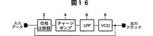
図16は、従来のPLL回路の構成図である。図16に示すように、PLL回路は、位相比較器2、チャージポンプ4、LPF6及び電圧制御発振回路(VCO)8より構成される。位相比較器2は、NRZデータ等の入力データとVCO8との出力クロックの位相を比較して、位相差を示す位相差信号(例えば、パルス幅で位相差を示す)をチャージポンプ4に出力する。チャージポンプ4は、位相差信号を電流に変換して、出力電流を出力する。LPF6は、出力電流を平滑化する。VCO8は、LPF6の出力電圧に従った発振周波数で発振して、クロックを出力する。VCO8の出力クロックを位相比較器2に入力して、VCO8にフィードバックすることにより、入力データに同期したクロックを得ている。
FIG. 16 is a configuration diagram of a conventional PLL circuit. As shown in FIG. 16, the PLL circuit includes a
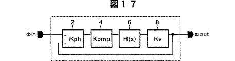
図17は、図16のブロック線図である。図17により、このPLL回路のフィードバックループの閉ループゲインは、式(1)で表される。また、開ループゲインは、式(2)で表される。 FIG. 17 is a block diagram of FIG. As shown in FIG. 17, the closed loop gain of the feedback loop of the PLL circuit is expressed by Expression (1). Further, the open loop gain is expressed by Expression (2).
開ループゲイン=Kph・Ipmp・F(s)・Kv/s ・・・(1)
閉ループゲイン=Φout/Φin
=Kph・Ipmp・F(s)・Kv/{s+Kph・IpmpF(s)Kv}
・・・(2)
但し、Kphは位相比較器利得であり、例えば、パルス幅/位相差(s/rad)、Ipmpはチャージポンプ電流振幅値(A)、F(s)はLPF伝達関数であり、例えば、電圧/電流値(Ω)、KvはVCO利得であり、周波数/電圧(Hz/V)である。
Open loop gain = Kph, Ipmp, F (s), Kv / s (1)
Closed loop gain = Φout / Φin
= Kph · Impmp · F (s) · Kv / {s + Kph · ImpmpF (s) Kv}
... (2)
Where Kph is a phase comparator gain, for example, pulse width / phase difference (s / rad), Ipmp is a charge pump current amplitude value (A), and F (s) is an LPF transfer function, for example, voltage / The current value (Ω) and Kv are VCO gains and are frequency / voltage (Hz / V).
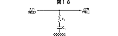
図18は、完全2次型ループフィルタを示す図である。図18に示す完全2次型ループのF(s)は、式(3)で表される。 FIG. 18 is a diagram illustrating a complete second-order loop filter. F (s) of the complete quadratic loop shown in FIG.
F(s)=R1(1+1/sC1・R1) ・・・(3)
完全2次型ループフィルタをPLL回路に使用した場合の開ループゲイン、閉ループゲインは、式(3)を式(1),(2)にそれぞれ代入すると、式(4),(5)となる。
F (s) = R1 (1 + 1 / sC1 · R1) (3)
The open loop gain and the closed loop gain when a complete secondary loop filter is used in the PLL circuit are expressed by equations (4) and (5) when equation (3) is substituted into equations (1) and (2), respectively. .
開ループゲイン=(Kph・Ipmp・KvR1/s)・(1+1/sC1R1)
・・・(4)
閉ループゲイン={Kph・Ipmp・Kv・(1+sC1R1)}
/{s2C1+Kph・Ipmp・Kv・(1+sC1・R1)}
・・・(5)
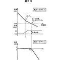
図19及び図20は、式(4),(5)で示されるPLL回路の周波数特性を示す図である。図19及び図20において、上段が開ループゲインのゲイン特性及び位相特性、下段が閉ループゲインを表している。図19は、ループ利得が大きい場合、図20は、ループ利得が小さい場合をそれぞれ示している。
Open loop gain = (Kph · Ipmp · KvR1 / s) · (1 + 1 / sC1R1)
... (4)
Closed loop gain = {Kph · Ipmp · Kv · (1 + sC1R1)}
/ {S 2 C1 + Kph · Ipmp · Kv · (1 + sC1 · R1)}
... (5)
19 and 20 are diagrams showing the frequency characteristics of the PLL circuit expressed by the equations (4) and (5). 19 and 20, the upper stage represents the gain characteristics and phase characteristics of the open loop gain, and the lower stage represents the closed loop gain. FIG. 19 shows a case where the loop gain is large, and FIG. 20 shows a case where the loop gain is small.
開ループゲインは、低周波側から1/R1C1まで12dB/octで減少し、1/R1C1以降は6dB/octで減少する。閉ループゲインのカットオフ周波数は、おおよそ開ループゲインが0dBになる周波数であり、式(6)により表されるループ利得に比例する。 The open loop gain decreases from the low frequency side to 1 / R1C1 at 12 dB / oct, and from 1 / R1C1 to 6 dB / oct. The cutoff frequency of the closed loop gain is a frequency at which the open loop gain becomes approximately 0 dB, and is proportional to the loop gain represented by the equation (6).
閉ループゲインのカットオフ周波数≒ループ利得=Kph・Ipmp・Kv・R1
・・・(6)
尚、式(6)では、1≪R1C1としている。
Closed loop gain cutoff frequency ≒ Loop gain = Kph, Ipmp, Kv, R1
... (6)
In Equation (6), 1 << R1C1.
従って、閉ループゲインのカットオフ周波数は、位相比較器、チャージポンプ、VCOの利得のそれぞれに比例して大きくなる。 Therefore, the cutoff frequency of the closed loop gain increases in proportion to the gains of the phase comparator, charge pump, and VCO.
図19に示すようにループ利得が大きい場合、位相余裕が大きく(90deg)、カットオフ周波数は大きくなる。逆に、図20に示すようにループ利得が小さい場合、位相余裕が小さく(45deg程度)なるためピーキングが大きくなり、カットオフ周波数は小さくなる。カットオフ周波数が大きくなると、高周波の位相のゆらぎがカットされず、ジッタが大きくなる。一方、位相余裕が小さくなってピーキングが大きくなると、位相のゆらぎ、即ち、ジッタが大きくなる。一般に、閉ループゲイン特性はジッタトランスファにより規定される。光通信等においてクロック抽出に用いられるPLL回路の閉ループゲインは、ITU−T勧告G958のSTM−1のジッタトランスファの仕様により規定される。 As shown in FIG. 19, when the loop gain is large, the phase margin is large (90 deg) and the cutoff frequency is large. Conversely, as shown in FIG. 20, when the loop gain is small, the phase margin is small (about 45 degrees), so that peaking increases and the cut-off frequency decreases. When the cut-off frequency is increased, the high-frequency phase fluctuation is not cut and the jitter is increased. On the other hand, when the phase margin decreases and the peaking increases, the phase fluctuation, that is, jitter increases. In general, the closed loop gain characteristic is defined by jitter transfer. The closed loop gain of the PLL circuit used for clock extraction in optical communication or the like is defined by the STM-1 jitter transfer specification of ITU-T recommendation G958.
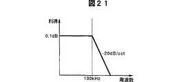
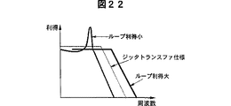
図21はITI−T勧告G958のSTM−1のジッタトランスファの仕様を示す図である。図21に示すように、この仕様では、カットオフ周波数は130kHz以下、ピーキングは0.1dB以下である。 FIG. 21 is a diagram showing the specifications of the jitter transfer of STM-1 of ITI-T recommendation G958. As shown in FIG. 21, in this specification, the cutoff frequency is 130 kHz or less and the peaking is 0.1 dB or less.
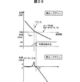
図22は、ループ利得が変動した場合のPLL周波数特性を示す図である。ループ利得が小さすぎる場合、図22に示すように、ピーキング仕様を満足できない。逆に、ループ利得が大きすぎると場合、図22に示すように、カットオフの仕様を満足できない。従って、ジッタトランスファ満足するためには、PLL回路のループ利得を、ピーキングの仕様から決まる下限値とカットオフ周波数の仕様から決まる上限値の間にあるように設計する必要がある。 FIG. 22 is a diagram illustrating the PLL frequency characteristics when the loop gain varies. If the loop gain is too small, the peaking specification cannot be satisfied as shown in FIG. On the other hand, if the loop gain is too large, the cutoff specification cannot be satisfied as shown in FIG. Therefore, in order to satisfy the jitter transfer, it is necessary to design the loop gain of the PLL circuit to be between the lower limit value determined from the peaking specification and the upper limit value determined from the cutoff frequency specification.
しかし、高周波で動作するVCOを設計した場合、プロセス、温度、電源弾圧に依存してVCO利得KVが大きく変動するため、ループ利得が大きくばらつき、ジッタトランスファ特性を満足させることが困難である。 However, when a VCO that operates at a high frequency is designed, the VCO gain KV varies greatly depending on the process, temperature, and power supply suppression, so that the loop gain varies greatly and it is difficult to satisfy the jitter transfer characteristics.
この問題に対して、特願平8−310804は、PLL回路の周波数収束特性からVCO利得を検出し、PLL回路のループ利得を補償することを開示している。この例では、PLL回路が収束していく段階のVCO制御電圧の時間変化から、VCO利得Kvを検出している。VCO制御電圧の時間変化をA/D変換器でサンプリングして、DSPで計算してVCO利得を検出・補償している。しかし、VCO制御電圧の時間変化を検出するためには、一旦、PLL回路のロックを外す必要があるため、通信装置等のように連続動作中に温度、電源電圧の変化によるVCO利得の変化に対応できないという問題があった。また、A/D変換回路、DSPを必要とするため、回路が複雑になっていた。 In response to this problem, Japanese Patent Application No. 8-310804 discloses that the VCO gain is detected from the frequency convergence characteristic of the PLL circuit and the loop gain of the PLL circuit is compensated. In this example, the VCO gain Kv is detected from the time change of the VCO control voltage when the PLL circuit converges. The time change of the VCO control voltage is sampled by an A / D converter and calculated by a DSP to detect and compensate for the VCO gain. However, in order to detect the time change of the VCO control voltage, it is necessary to once unlock the PLL circuit, so that the change in the VCO gain due to the change in temperature and power supply voltage during continuous operation like a communication device or the like. There was a problem that could not be handled. Further, since an A / D conversion circuit and a DSP are required, the circuit is complicated.
本発明の目的は、簡単な回路構成により連続動作中にVCO利得を測定して、PLL回路の利得を一定にするPLL回路を提供することである。 An object of the present invention is to provide a PLL circuit that measures the VCO gain during continuous operation with a simple circuit configuration and makes the gain of the PLL circuit constant.
本発明の側面によれば、利得制御機能を有するPLL回路であって、第1入力信号と第2入力信号の位相差を示す第1位相差信号を出力する第1位相比較器と、前記第1位相差信号に基づく信号を平滑化して、第1制御電圧を出力する第1ループフィルタと、前記第1制御電圧に基づく周波数で発振して、第1クロックを出力するVCO(電圧制御発振回路)と、第2制御電圧に基づく周波数で発振して、第2クロックを出力する前記VCOと同一特性のダミーVCOと、前記第1及び第2クロックの周波数差と前記第1及び第2制御電圧の電圧差とに基いて、前記VCOの利得を検出するVCO利得検出回路と、前記VCO利得検出回路が検出した前記VCOの利得に基いて、ループ利得が一定になるように制御する利得制御回路と、前記第1制御電圧にオフセット電圧を加算して、加算された電圧を前記第2制御電圧として前記ダミーVCOに出力するオフセット回路とを具備し、前記第2入力信号は、前記第1クロックに基く信号であることを特徴とする利得制御機能を有するPLL回路が提供される。 According to an aspect of the present invention, a PLL circuit having a gain control function, the first phase comparator outputting a first phase difference signal indicating a phase difference between the first input signal and the second input signal, A first loop filter that smoothes a signal based on one phase difference signal and outputs a first control voltage, and a VCO (voltage controlled oscillation circuit) that oscillates at a frequency based on the first control voltage and outputs a first clock ), A dummy VCO having the same characteristics as the VCO that oscillates at a frequency based on the second control voltage and outputs a second clock, the frequency difference between the first and second clocks, and the first and second control voltages And a gain control circuit for controlling the loop gain to be constant based on the gain of the VCO detected by the VCO gain detection circuit. and, the 1 control voltage by adding an offset voltage to, comprises an offset circuit for outputting the dummy VCO the added voltage as said second control voltage, said second input signal is a signal based on the first clock A PLL circuit having a gain control function is provided.
動作環境の変動により、VCOの利得が変動する。VCO利得検出回路は、VCOと同一特性のダミーVCOを用いて、PLL回路がロックしたときのVCOの第1発振周波数f1、VCOに印加する第1制御電圧V1、ダミーVCOに印加する第2制御電圧V2、ダミーVCOの第2発振周波数f1に従って、(Δf2−Δf1)/Δ(V2−V1)により、VCOの利得を検出する。このVCOの利得に従って、PLL回路のループ利得が一定になるように、制御する。これにより、VCOの利得が変動しても、PLL回路がジッタトランスファの仕様を満足する。 The gain of the VCO varies due to variations in the operating environment. The VCO gain detection circuit uses a dummy VCO having the same characteristics as the VCO, and uses a first control frequency V1 applied to the VCO when the PLL circuit is locked, a first control voltage V1 applied to the VCO, and a second control applied to the dummy VCO. According to the second oscillation frequency f1 of the voltage V2 and the dummy VCO, the gain of the VCO is detected by (Δf2−Δf1) / Δ (V2−V1). Control is performed so that the loop gain of the PLL circuit becomes constant according to the gain of the VCO. Thereby, even if the gain of the VCO fluctuates, the PLL circuit satisfies the jitter transfer specifications.
本発明によると、VCOと同一特性のダミーVCOを用いて、PLL回路がロックしたときのVCOの発振周波数、VCOに印加する制御電圧、ダミーVCOに印加する制御電圧、ダミーVCOの発振周波数に従って、VCOの利得を検出して、このVCOの利得に従って、PLL回路のループ利得が一定になるように、制御する。これにより、VCOの利得が変動しても、PLL回路がジッタトランスファの仕様を満足する。 According to the present invention, using a dummy VCO having the same characteristics as the VCO, according to the oscillation frequency of the VCO when the PLL circuit is locked, the control voltage applied to the VCO, the control voltage applied to the dummy VCO, and the oscillation frequency of the dummy VCO, The gain of the VCO is detected, and the loop gain of the PLL circuit is controlled to be constant according to the gain of the VCO. Thereby, even if the gain of the VCO fluctuates, the PLL circuit satisfies the jitter transfer specifications.
また、本発明によると、ディジタルデータのエッジ率を検出して、エッジ率が示す位相比較器の利得に従って、PLL回路のループ利得が一定となるように、制御する。そのため、位相比較器の利得がエッジ率の変動に起因して、変動しても、PLL回路がジッタトランスファの仕様を満足する。 According to the present invention, the edge rate of the digital data is detected and controlled so that the loop gain of the PLL circuit becomes constant according to the gain of the phase comparator indicated by the edge rate. Therefore, even if the gain of the phase comparator varies due to the variation of the edge rate, the PLL circuit satisfies the jitter transfer specifications.
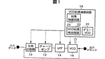
発明を実施するための最良の態様の説明をする前に本発明の原理を説明する。図1は本発明の原理図である。図1に示すように、PLL回路は、位相比較器10、チャージポンプ12、LPF14、VCO16及びVCO利得補償回路18を具備する。VCO利得補償回路18は、ダミーVCO20、VCO利得検出回路22及び利得制御回路24を有する。
Before describing the best mode for carrying out the invention, the principle of the present invention will be described. FIG. 1 shows the principle of the present invention. As shown in FIG. 1, the PLL circuit includes a
位相比較器10には、光通信等のNRZデータ等の入力データ及びVCO16の出力クロックが入力される。位相比較器10は、入力データ及びVCO16の出力クロックの位相差を検出して、位相差を示す位相差信号を出力する。この位相差信号は、例えば、位相差をパルス幅で示す信号である。チャージポンプ12は、位相差信号を電流に変換して、LPF14に出力する。LPF14は、チャージポンプ12の出力電流を電圧Vに変換して、VCO16に出力する。VCO16は、電圧Vに従った周波数で発振してクロックを出力する。
The
VCO16の利得は、動作環境により変動する。VCO利得検出回路22は、VCO16と同一の特性を有するダミーVCO20を用いて、VCO16の利得を検出する。例えば、PLL回路がロックしたときの、動作中におけるVCO16の出力周波数、電圧Vにオフセット電圧ΔVを加えた電圧(V+ΔV)をダミーVCO20の出力周波数及びオフセット電圧ΔVによりVCO16の利得を検出することができる。利得制御回路24は、VCO16の利得よりPLL回路のループ利得が一定となるように、位相比較器10、チャージポンプ12、LPF14やVCO16の利得を制御する。これにより、VCO16の利得が変動しても、PLL回路が動作中に、PLL回路の利得を一定にすることができる。
The gain of the
第1実施形態
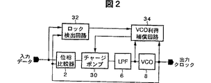
図2は、本発明の第1実施形態によるPLL回路の構成図であり、図16中の構成要素と実質的に同一の構成要素には同一の符号を付している。図2に示すPLL回路は光通信のクロック抽出回路等に使用されるものである。このPLL回路は、位相比較器2、チャージポンプ30、LPF6、VCO8、ロック検出回路32及びVCO利得補償回路34を具備する。
First Embodiment FIG. 2 is a block diagram of a PLL circuit according to a first embodiment of the present invention. Components that are substantially the same as those in FIG. 16 are given the same reference numerals. The PLL circuit shown in FIG. 2 is used for an optical communication clock extraction circuit or the like. This PLL circuit includes a
位相比較器2は、入力データとVCO8の出力クロックの位相差を検出して、位相差をパルス幅で示すパルス信号及び位相の遅れ/進みを示すUP/DOWN信号からなる位相差信号を出力する。チャージポンプ30は、VCO利得補償回路32により出力振幅電流値Ipmpが制御される正電流源回路及び負電流源回路と、正定電流源回路とLPF6との間を接続する第1スイッチ及び負定電流源回路とLPF6との間を接続する第2スイッチを有する。UP信号/DOWN信号により第1/第2スイッチがパルス信号のパルス幅だけオンして、出力電流Ipmp又は−IpmpをLPF6に出力する。
The
LPF6は、チャージポンプ30の出力電流を平滑化して、平滑化電圧Vを出力するものであり、例えば、図18に示した完全2次型フィルタである。VCO8は、LPF6の出力電圧Vに従った発振周波数で発振して、出力クロックを出力するものであり、例えば、リング発振器である。ロック検出回路32は、VCO8の出力クロックと入力データの位相が一致してPLL回路がロックしたことを検出して、ロック検出信号をVCO利得補償回路34に出力する。
The
VCO利得補償回路34は、PLL回路がロックしたときのVCO8の出力周波数f1と、そのときのLPF6の出力電圧Vにオフセット電圧ΔVを加えた電圧(V+ΔV)をVCO8と同じ利得を有するダミーVCOに印加したときの出力周波数f2とから、式(7)で示されるVCO8の利得Kvを測定する。
The VCO
Kv=VCO8の出力周波数の変化/電圧の変化
=(f2−f1)/ΔV ・・・(7)
式(7)中で、f2はVCO8の電圧(V+ΔV)での出力周波数であることが望ましいが、VCO8がロックしている間はVCO8の出力周波数を変更できない。そこで、VCO8と同じ特性を有するダミーVCOを用いて、出力周波数f2を測定する。このとき、ダミーVCOも動作環境の変化により利得が変動するが、VCO8と動作環境が同じなので、変動した利得もまたVCO8と同一であると推定される。そのため、VCO8の利得Kvが検出される。
Kv = change in output frequency of VCO8 / change in voltage = (f2-f1) / ΔV (7)
In equation (7), f2 is preferably the output frequency at the voltage (V + ΔV) of the
温度変化、電源電圧等の動作環境の変化によるVCO8の利得Kvの変動分を補償して、PLL回路がジッタトランスファの仕様を満足するループ利得に一致させるべくチャージポンプ30の利得Ipmpと利得Kvとの積Ipmp×Kvが目標値Cに一致するようにチャージポンプ30のゲイン(定電流源回路の振幅電流)を制御する。
The gain Ipmp and gain Kv of the
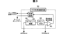
図3は、図2中のVCO利得補償回路34の構成図である。図3に示すように、VCO利得制御回路34は、オフセット回路36、ダミーVCO38、周波数差検出回路40及び制御回路42を有する。オフセット回路36は、LPF6の出力電圧Vにオフセット電圧ΔVを加算して、電圧(V+ΔV)を出力する。尚、オフセット電圧ΔVは、式(7)で示される利得Kvの測定精度が最も良好な値とする。ダミーVCO38は、オフセット回路36の出力電圧(V+ΔV)に従って発振して、出力周波数f2の出力クロックを出力するものであり、VCO8と同一特性を有する。周波数差検出回路40は、ダミーVCO38の出力周波数f2とVCO8の出力周波数f1との差分を検出する。
FIG. 3 is a block diagram of the VCO
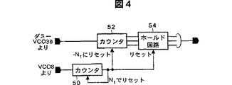
図4は、図3中の周波数差検出回路40の構成図である。図4に示すように、周波数差検出回路40は、カウンタ50,52及びホールド回路54を有する。カウンタ50は、VCO8の出力クロックをカウントして、固定値N1になるとリセット信号を出力する。リセット信号は、カウンタ50を0に、カウンタ52を−N1にリセットする。カウンタ52は、ダミーVCO38の出力クロックをカウントして、リセット信号により−N1にリセットされる。ホールド回路54は、リセットがかかる直前のカウンタ52のカウンタ値N2を次のリセットまで保持するものであり、例えば、フリップフロップである。
FIG. 4 is a configuration diagram of the frequency
VCO8の出力周波数はf1なので、カウンタ50がN1カウントするまでの時間はN1/f1である。カウンタ52は、N1/f1の間にN1/f1÷(1/f2)=(N1×f2/f1)回をカウントする。よって、−N1にリセットされる直前のカウンタ52のカウント値N2は、(N1×f2/f1−N1)=((f2−f1)/f1)×N1となる。よって、ホールド回路54には、N2=((f2−f1)/f1)×N1がホールドされる。PLL回路がロックしている時、周波数f1が入力データのビットレートの周波数であり、一定であるため、N2の値は周波数差(f2−f1)に比例していることになる。
Since the output frequency of the
図3中の制御回路42は、ロック検出信号がPLL回路のロックを示すとき、周波数差検出回路40から出力されるN2=((f2−f1)/f1)×N1から周波数差(f2−f1)を取り出す。式(7)に示されるVCO8の利得Kv=(f2−f1)/ΔVを計算する。チャージポンプ30の利得Ipmp=上記目標値C÷測定された利得Kvを計算する。
When the lock detection signal indicates that the PLL circuit is locked, the
以下、図2のPLL回路の動作説明をする。 The operation of the PLL circuit of FIG. 2 will be described below.
(a) 位相同期
位相比較器2には、光通信等の入力データであるNRZデータ及びVCO8の出力クロックが入力される。位相比較器2は、NRZデータとVCO8の出力クロックの位相を比較して、位相差をパルス幅で示すパルス信号及びNRZデータに対する出力クロックの位相の進み/遅れを示すUP/DOWN信号からなる位相差信号をチャージポンプ30に出力する。VCO利得補償回路34は、ロック検出信号がPLL回路がロックしていないことを示す場合は、上記目標値C÷(標準的な動作環境で予測されるVCO8の利得Kv)がチャージポンプ30の利得となるように制御する。チャージポンプ30は、VCO利得補償回路34により制御される電流振幅Ipmpの出力電流をLPF6に出力する。
(A) Phase synchronization The
LPF6は、例えば、完全2次型フィルタにより、チャージポンプ30の出力電流を平滑化して、平滑化電圧Vを出力する。VCO8は、例えば、リング発振器により、LPF6の出力電圧Vに従った発振周波数で発振して、出力クロックを出力する。VCO8の出力クロックは、位相比較器2にフィードバック入力される。位相比較器2、チャージポンプ30及びLPF6により、VCO8の周波数がNRZデータの位相に一致するよう制御される。その結果、PLL回路がロックする。
The
(b) ロック検出
ロック検出回路32は、NRZデータとVCO8の位相を比較して、その位相が一致するか否かを検出することにより、PLL回路がロックしているか否かを示すロック検出信号をVCO利得補償回路34に出力する。
(B) Lock detection The
(c) VCO8の利得検出
VCO利得補償回路34中のオフセット回路36は、LPF6の出力電圧Vにオフセット電圧ΔVを加算して、電圧(V+ΔV)をダミーVCO38に出力する。周波数差検出回路40中のカウンタ50は、VCO8の出力クロックをカウントして、固定値N1になるとリセット信号を出力する。リセット信号は、カウンタ50を0に、カウンタ52を−N1にリセットする。カウンタ52は、ダミーVCO38の出力クロックをカウントして、リセット信号により−N1にリセットされる。ホールド回路54は、リセットがかかる直前のカウンタ52のカウンタ値N2=((f2−f1)/f1)×N1を次のリセットまで保持する。ダミーVCO38は、電圧(V+ΔV)に従って、発振周波数f2の出力クロックを出力する。図3中の制御回路42は、ロック検出信号がPLL回路のロックを示すとき、周波数差検出回路40から出力されるN2=((f2−f1)/f1)×N1から周波数差(f2−f1)を取り出す。VCO8の利得Kv=(f2−f1)/ΔVを計算する。
(C)
(d) チャージポンプ30の利得制御
制御回路42は、チャージポンプ30の利得Ipmp=(上記目標値C÷検出された利得Kv)を計算する。計算された利得Ipmpとなるようにチャージポンプ30の定電流源回路を制御する。チャージポンプ30は、制御回路42の制御に従って、利得Ipmpの電流振幅の出力電流をLPF6に出力する。この結果、VCO8の利得が温度変化や電源電圧の変動により変化しても、PLL回路のループ利得が一定になり、PLL回路がジッタトランスファの仕様を満足する。しかも、PLL回路が動作中にロックを外すことなくPLL回路のループ利得が一定とるように制御できる。
(D) Gain Control of
第2実施形態
図5は、本発明の第2実施形態によるPLL回路の構成図であり、図2中の構成要素と実質的に同一の構成要素には同一の符号を附している。図5に示すように、PLL回路は、位相比較器2、チャージポンプ30、LPF6、VCO8、ロック検出回路32及びVCO利得補償回路60を具備する。
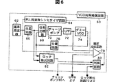
Second Embodiment FIG. 5 is a block diagram of a PLL circuit according to a second embodiment of the present invention. Components substantially the same as those in FIG. 2 are denoted by the same reference numerals. As shown in FIG. 5, the PLL circuit includes a
VCO利得補償回路60は、VCO8と同一特性のダミーVCOを含むPLL周波数シンセサイザ回路を有する。そして、NRZデータのビットレートの既知の周波数f1にPLL回路がロックしたときのLPF6の出力電圧V1と、PLL周波数シンセサイザ回路が既知の周波数f2にロックしたときLPFの出力電圧V2、及び周波数差(f2−f1)によりVCO8の利得Kvを検出して、PLL回路のループ利得が一定となるように、チャージポンプ30の利得を制御する。
The VCO
図6は、図5中のVCO利得補償回路60の構成図である。図6に示すように、VCO利得補償回路60は、基準周波数発振回路62、ダミー周波数シンセサイザ回路64、電圧比較回路78及び制御回路80を有する。基準周波数発振回路62は、基準周波数f3のクロック信号を出力する。PLL周波数シンセサイザ回路64は、分周回路66、位相比較器68、チャージポンプ70、LPF72、ダミーVCO74及び分周回路76を有する。
FIG. 6 is a configuration diagram of the VCO
分周回路66は、基準周波数f3の基準クロックを分周比1/N1に分周して、周波数f3/N1のクロックを出力する。位相比較器68は、分周回路66の出力クロックと分周回路76の出力クロックの位相差を検出して、位相差をパルス幅で示すパルス信号及び位相の遅れ/進みを示すUP/DOWN信号からなる位相差信号を出力する。チャージポンプ70は、パルス信号を電流に変換して、LPF72に出力する。LPF72は、チャージポンプ70の出力電流を平滑化して、平滑化電圧V2を出力する。ダミーVCO74は、LPF72の出力電圧V2に従った発振周波数f2で発振して、出力クロックを出力する。分周回路76は、周波数f2の出力クロックを分周比1/N2で分周する。尚、PLL周波数シンセサイザ回路64がロックしたとき、f2=(f3×N2)/N1となる。
The
電圧比較回路78は、LPF6の出力電圧V1とLPF72の出力電圧V2の差分電圧ΔV=(V2−V1)を求めるものであり、例えば、オペアンプである。制御回路80は、ロック検出回路32,82のロック検出信号がPLL回路及びPLL周波数シンセサイザ回路64がロックしたことを示すとき、ダミーVCO74の既知の周波数f2、入力データのビットレートの既知の周波数f1及び差分電圧ΔVより、式(8)に示されるVCO8の利得Kvを計算する。
The
Kv=(f2−f1)/ΔV ・・・(8)
制御回路80は、チャージポンプ30の利得Ipmp=(上記目標値C÷式(8)により検出された利得KV)を計算する。計算された利得Ipmpとなるようにチャージポンプ30の定電流源回路を制御する。ロック検出回路82は、分周回路68,76の出力クロックを比較して、PLL周波数シンセサイザ回路64がロックしたか否かを検出して、ロック検出信号を出力する。
Kv = (f2-f1) / ΔV (8)
The
以下、図5のPLL回路の動作説明をする。 The operation of the PLL circuit in FIG. 5 will be described below.
(a) 第1実施形態の(a)と同様にして、位相同期が取られる。 (A) Phase synchronization is achieved in the same manner as (a) of the first embodiment.
(b) ロック検出
ロック検出回路32は、NRZデータとVCO8の位相を比較して、その位相が一致するか否かを検出して、ロック検出信号をVCO利得補償回路34に出力する。一方、ロック検出回路82は、分周回路68,76の出力クロックを比較して、PLL周波数シンセサイザ回路64がロックしたか否かを検出して、ロック検出信号を出力する。
(B) Lock detection The
(c) VCO8の利得検出
VCO利得補償回路60中の基準周波発振回路62は、周波数数f2のクロック信号を出力する。分周回路66は、基準周波数f3の基準クロックを分周比1/N1に分周して、周波数f3/N1のクロックを出力する。位相比較器68は、分周回路66の出力クロックと分周回路76の出力クロックの位相差を検出して、位相差をパルス幅で示すパルス信号及び位相の遅れ/進みを示すUP/DOWN信号からなる位相差信号を出力する。チャージポンプ70は、パルス信号を出力電流Ipmp又は−Ipmpに変換して、LPF72に出力する。LPF72は、チャージポンプ70の出力電流を平滑化して、平滑化電圧V2を出力する。
(C)
ダミーVCO74は、LPF72の出力電圧V2に従った発振周波数f2で発振して、出力クロックを出力する。分周回路76は、周波数f2の出力クロックを分周比1/N2で分周する。但し、PLL周波数シンセサイザ回路64がロックしたとき、f2=(f3×N2)/N1となる。電圧比較回路78は、LPF6の出力電圧V1とLPF72の出力電圧V2の差分電圧ΔV=(V2−V1)を求める。制御回路80は、ロック検出回路32及び82のロック検出信号がPLL回路及びPLL周波数シンセサイザ回路64がロックしたことを示すとき、ダミーVCO72の既知の周波数f2、入力データのビットレートの周波数f1及び差分電圧ΔVより、式(8)に示されるVCO8の利得Kvを計算する。
The
(d) チャージポンプ30の利得制御
制御回路80は、チャージポンプ30の利得Ipmp=(上記目標値C÷式(8)により検出された利得Kv)を計算する。チャージポンプ30は、制御回路80の制御に従って、利得Ipmpの電流振幅の電流をLPF6に出力する。この結果、VCO8の利得が温度変化や電源電圧の変動により変化しても、PLL回路のループ利得が一定になり、PLL回路がジッタトランスファの仕様を満足する。
(D) Gain Control of
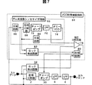
第3実施形態
図7は、本発明の第3実施形態によるPLL回路の構成図であり、図5及び図6中の構成要素と実質的に同一の構成要素には同一の符号を附している。VCO利得補償回路84中の分周回路86の入力クロックをVCO8の出力クロックとしたことが、図6中のVCO利得補償回路60と異なる。PLLシンセサイザ回路85中の分周回路86,88の分周比N3,N4は、PLL回路がロックしたときのVCO8の発振周波数f1、ダミーVCO74の発振周波数f2=(f1×N4)/N3としたとき、VCO8の利得Kvが精度良く測定できる値としている。図7のPLL回路の動作は、分周回路86にVCO8の出力クロックが入力される点を除いて、図6のPLL回路と同様なので説明を省略する。
Third Embodiment FIG. 7 is a block diagram of a PLL circuit according to a third embodiment of the present invention. Components that are substantially the same as those in FIGS. 5 and 6 are given the same reference numerals. Yes. The difference from the VCO
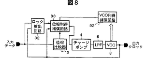
第4実施形態
図8は、本発明の第4実施形態によるPLL回路の構成図であり、図2中と実質的に同一の構成要素には同一の符号を附している。図5に示すように、PLL回路は、位相比較器2、チャージポンプ4、LPF6、VCO8、ロック検出回路32、位相利得補償回路90及びVCO利得補償回路92を具備する。
Fourth Embodiment FIG. 8 is a block diagram of a PLL circuit according to a fourth embodiment of the present invention. Components substantially the same as those in FIG. 2 are denoted by the same reference numerals. As shown in FIG. 5, the PLL circuit includes a
位相比較器利得制御回路90は、VCO利得補償回路92から出力されるVCO8の利得Kvに反比例する式(9)で示される値Mを元に、位相比較器2のパルス信号を概ね(N−M)/Nの確率でマスクして、位相比較器2の利得Kphを制御する。
The phase comparator
M=(Kvmin /Kv)×N ・・・(9)
但し、KvminはVCO8の動作環境等により予測される最小利得、KvはVCO8の利得である。位相比較器2の利得を制御する周期をTとすると、N=T/f1である。f1はNRZデータのビットレートに等しい周波数である。
M = (Kvmin / Kv) × N (9)
However, Kvmin is the minimum gain predicted by the operating environment of the
VCO8の利得が最小利得Kvminであるときに、PLL回路のループ利得がジッタトランスファを満足するように、位相比較器2の利得Kph、チャージポンプ4の利得Ipmp及びLPF6の伝達関数が設定されている。このとき、利得Kvminと位相比較器2のパルス信号をスルーしたときの利得Kphとの積をC2とする。(N−M)/N(0≦M≦N)の確率でパルス信号をマスクして、M/Nの確率でスルーすると、その利得Kph1は(Kph×M)/Nに概略一致する。Kph1とVCO8の利得Kvとの積はC2となり、PLL回路のループ利得が概略一定となる。
When the gain of the
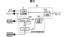
図9は、図8中の位相利得補償回路90の構成図である。図9に示すように、位相利得補償回路90は、カウンタ96、メモリ98、比較回路100及びマスク回路102を有する。カウンタ96は、ロック検出信号がPLL回路のロックを示すとき、VCO8の出力クロックをカウントして、カウント値=Nになると、カウント値=0にリセットされる。ロック検出信号がPLL回路のロックを示さないときは、カウント値=0のままであり、カウント動作を停止している。メモリ98には、VCO利得補償回路92より値Mが書き込まれる。比較回路100は、カウンタ96のカウント値とメモリ98の記憶値Mを比較し、カウント値がMより小さいとき’L’、大きいとき’H’を出力する。マスク回路102は、比較回路100の出力が’L’の間は位相比較器2の出力をそのまま出力し、’H’になると、マスクする。VCO利得補償回路92は、第1〜第3実施形態と同様にして、VCO8の利得Kvを検出する。そして、式(9)で表される値Mを計算して、メモリ98に書き込む。
FIG. 9 is a configuration diagram of the phase
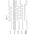
図10は、図9のタイムチャートである。以下、図10を参照して、図8の動作説明をする。 FIG. 10 is a time chart of FIG. The operation of FIG. 8 will be described below with reference to FIG.
(a) 第1実施形態の(a)と同様にして、位相同期が取られる。 (A) Phase synchronization is achieved in the same manner as (a) of the first embodiment.
(b) ロック検出回路32は、NRZデータとVCO8の位相を比較して、その位相が一致するか否かを検出して、ロック検出信号を位相利得補償回路90に出力する。
(B) The
(c) VCO8の利得検出
VCO利得補償回路92は、第1〜第3実施形態と同様にして、VCO8の利得Kvを検出する。そして、式(9)で表される値Mを計算して、図9中のメモリ98に書き込む。
(C)
(d) 位相比較器2の利得制御
カウンタ96は、ロック検出信号がPLL回路のロックを示すとき、VCO8の出力クロックをカウントして、カウント値=Nになると、カウント値=0にリセットされる。尚、ロック検出信号がPLL回路のロックを示さないときは、カウント値=0であり、カウント動作が停止している。比較回路100は、カウンタ96のカウント値とメモリ98の記憶値Mを比較し、カウント値がMより小さいとき’L’、大きいとき’H’を出力する。マスク回路102は、図10に示すように、比較回路100の出力が’L’の間は位相比較器2の出力をそのまま出力し、’H’になると、マスクする。この結果、比較回路100の出力は、各N/f1周期(f1はVCO8の出力クロック周波数)毎に、(N−M)/f1の期間が’H’、M/f1の期間が’L’となるので、位相比較器2のパルス信号は、(N−M)/Nの確率でマスクされる。これにより、マスク回路102よりマスクされた位相比較器2のパルス信号については、利得Kph1が概略、Kph×M/N=Kph×(Kvmin/Kv)に一致する。Kph1×Kv=C2となり、エッジ率及びVCO8の利得が変動しても、PLL回路のループ利得が概略一定となる。
(D) Gain control of the
第5実施形態
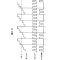
図11は、本発明の第5実施形態によるPLL回路の構成図であり、図2中と実質的に同一の構成要素には同一の符号を附している。図11に示すように、PLL回路は、位相比較器2、チャージポンプ4、フィルタ112、ロック検出回路32、VCO120及びVCO利得補償回路122を具備する。
Fifth Embodiment FIG. 11 is a block diagram of a PLL circuit according to a fifth embodiment of the present invention. Components substantially the same as those in FIG. 2 are denoted by the same reference numerals. As shown in FIG. 11, the PLL circuit includes a
VCO利得補償回路112は、第1〜第3実施形態と同様にして、VCO8の利得を検出して、PLL回路のループ利得が一定となるように、LPF110の伝達関数を制御する。LPF110は、VCO利得補償回路112により、その伝達関数が制御されるループフィルタである。本実施形態では、LPF110を図18に示す完全2次型フィルタで構成する。このとき、LPF110の抵抗を可変抵抗とする。LPF110を完全2次型フィルタで構成する場合は、PLL回路のループ利得は式(6)で示されるので、ジッタトランスファを満足するように、位相比較器2の利得、チャージポンプ4の利得、LPF110の抵抗及びVCO8の利得が設定されている。このときの、LPF110の抵抗とVCO8の利得との積をC3とする。VCO利得補償回路112は、測定したVCO8の利得KVとLPF110の抵抗値の積がC3に等しくなるように、LPF110の抵抗値を制御する。
Similarly to the first to third embodiments, the VCO
以下、図11のPLL回路の動作説明をする。 Hereinafter, the operation of the PLL circuit of FIG. 11 will be described.
(a) 第1実施形態の(a)と同様にして、PLL回路のVCO8の出力クロックとNRZデータとの位相同期が取られる。
(A) In the same manner as (a) of the first embodiment, the phase synchronization between the output clock of the
(b) ロック検出回路32は、NRZデータとVCO8の位相を比較して、その位相が一致するか否かを検出して、ロック検出信号をVCO利得補償回路112に出力する。
(B) The
(c) VCO8の利得検出
VCO利得補償回路112は、第1〜第3実施形態と同様にして、VCO8の利得Kvを検出する。
(C)
(d) LPF112の抵抗制御
VCO利得補償回路112は、ロック検出回路32のロック検出信号がPLL回路のロックを示しているとき、R1=(上記C3÷検出したVCO8の利得Kv)を計算する。そして、LPF112の抵抗が計算した抵抗値R1となるように制御する。これにより、PLL回路のループ利得が一定となる。
(D) Resistance Control of
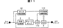
第6実施形態
図12は、本発明の第6実施形態によるPLL回路の構成図であり、図2中と実質的に同一の構成要素には同一の符号を附している。図12に示すように、PLL回路は、位相比較器2、チャージポンプ4、LPF6、ロック検出回路32、VCO120及びVCO利得補償回路122を具備する。VCO利得補償回路122は、第1〜第3実施形態と同様にして、VCO120の利得を検出して、PLL回路のループ利得が一定となるように、VCO120の利得を制御する。VCO120は、VCO利得補償回路122により、その利得が制御されるものである。VCO120としては、例えば、リング発振回路である。この場合、リング発振回路を構成するインバータの各遅延時間によりVCO120の利得が決定されるので、その遅延時間が所望の利得となるように制御される。
Sixth Embodiment FIG. 12 is a block diagram of a PLL circuit according to a sixth embodiment of the present invention. Components that are substantially the same as those in FIG. 2 are given the same reference numerals. As shown in FIG. 12, the PLL circuit includes a
以下、図11のPLL回路の動作説明をする。 Hereinafter, the operation of the PLL circuit of FIG. 11 will be described.
(a) 第1実施形態の(a)と同様にして、PLL回路のVCO120の出力クロックとNRZデータとの位相同期が取られる。
(A) In the same manner as (a) of the first embodiment, the phase synchronization between the output clock of the
(b) ロック検出回路32は、NRZデータとVCO120の位相を比較して、その位相が一致するか否かを検出して、ロック検出信号をVCO利得補償回路122に出力する。
(B) The
(c) VCO120の利得検出
VCO利得補償回路122は、第1〜第3実施形態と同様にして、VCO120の利得Kvを検出する。
(C)
(d) VCO120の利得制御
VCO利得補償回路122は、ロック検出回路32のロック検出信号がPLL回路のロックを示しているとき、VCO120の利得が一定となるように、VCO120を制御する。これにより、PLL回路のループ利得が一定となる。
(D) Gain Control of
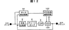
第7実施形態
図13は、本発明の第7実施形態によるPLL回路の構成図であり、図2中と実質的に同一の構成要素には同一の符号を附している。図13に示すように、PLL回路は、位相比較器2、チャージポンプ30、LPF6、VCO8、ロック検出回路32、位相比較利得検出回路132、VCO利得検出回路134及び利得制御回路136を具備する。
Seventh Embodiment FIG. 13 is a configuration diagram of a PLL circuit according to a seventh embodiment of the present invention, are denoted by the same reference numerals are essentially the same elements as those in FIG. As shown in FIG. 13, the PLL circuit includes a
クロック抽出用PLL回路では、通常、データのエッジが来た時のみ、クロックとデータの位相を比較するため、データパターンにより位相比較器2の利得Kphが大きく変動し、カットオフ周波数が大きく変動する。例えば、NRZデータが'10'の繰り返しパターンでは、立ち上がりエッジと立ち下りエッジが交互に来るため、エッジ率が100%であるのに対し、'1100'パターンでは、立ち上がりエッジ/立ち下りエッジともに4ビットに1回しか来ないため、エッジ率は50%になる。位相比較器利得Kphはエッジ率に比例するため、’10’と’1100’では、位相比較器2の利得Kphが2倍程度変動する。更に、同符号が連続した場合を考えると、位相比較器2の利得Kphはより大きく変動する問題があった。
In the clock extraction PLL circuit, since the phase of the clock and the data is normally compared only when the data edge comes, the gain Kph of the
位相比較利得検出回路132は、NRZデータのエッジ率を検出する。VCO利得検出回路134は、第1実施形態〜第3実施形態と同様にして、VCO8の利得Kvを検出する。エッジ率が一定、例えば、100%のときの位相比較器2の利得Kph、チャージポンプ30の利得Ipmp、LPF6の伝達関数F(s)及びVCO8の標準利得Kvにより決まるPLL回路のループ利得がジッタトランスファを満足するように各利得が決定されている。このときの位相比較器2の利得Kph×チャージポンプ30の利得Ipmp×VCO8の利得Kvとの積をC4とする。利得制御回路136は、K=C4÷(ロック中に検出された利得Kv×入力されたデータのエッジ率×エッジ率100%のときの位相利得Kph)を計算する。そして、利得制御回路136は、利得IpmpがKに等しくなるようにチャージポンプ30を制御する。
The phase comparison
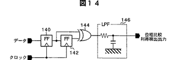
図14は、図13中の位相比較利得検出回路132の構成図である。図14に示すように、位相比較利得検出回路132は、フリップフロップ(FF)140、FF142、EX−ORゲート144及びLPF146を有する。FF140は、VCO8の出力クロックの立ち上がり又は立ち下りエッジのタイミングで、データをラッチする。FF142は、VCO8の出力クロックのエッジのタイミングで、FF140の出力をラッチする。例えば、FF140がNRZデータのNビット目を保持しているとき、FF142はNRZデータの(N−1)ビット目を保持する。
FIG. 14 is a configuration diagram of the phase comparison
EX−ORゲート146は、FF140,142の出力が一致((0,0)又は(1,1))するとき、’L’、一致しない((0,1)又は(1,0))のとき、’H’を出力する。この結果、XORゲート146の出力は、入力データのエッジが来たとき、”H”、エッジが来ないとき、”L”になる。LPF146は、EX−ORゲート144の出力を平均化する積分回路である。LPF146の出力電圧Vcが時定数τ(抵抗R×容量C)に従って変化するため、出力電圧Vcのレベルがエッジ率を表すように、時定数τを定める。例えば、エッジ率100%の入力データが継続して入力されたとき、LPF146の出力電圧VcがEX−ORゲート144の出力=’H’のときの電圧レベルViに一致するので、入力データのエッジ率α%としたときのLPF146の出力電圧Vc=α×Vi/100となるようにする。
When the outputs of the
図15は、図14のタイムチャートである。以下、この図面を参照して、図14のPLL回路の動作説明をする。 FIG. 15 is a time chart of FIG. The operation of the PLL circuit of FIG. 14 will be described below with reference to this drawing.
(a) 第1実施形態の(a)と同様にして、PLL回路のVCO8の出力クロックとNRZデータとの位相同期が取られる。
(A) In the same manner as (a) of the first embodiment, the phase synchronization between the output clock of the
(b) ロック検出回路32は、NRZデータとVCO8の出力クロックの位相を比較して、その位相が一致するか否かを検出して、ロック検出信号を利得制御回路136に出力する。
(B) The
(c) VCO8の利得検出
VCO利得補償回路122は、第1〜第3実施形態と同様にして、VCO8の利得Kvを検出して、利得制御回路136に出力する。
(C)
(d) 位相比較利得検出
位相比較利得検出回路132中のFF140は、VCO8の出力クロックのエッジにおいて、NRZデータをラッチする。FF142は、VCO8の出力クロックのエッジにおいて、FF140の出力をラッチする。EX−ORゲート146は、FF140,142の出力が一致するとき'L'、一致しないとき'H'を出力する。この結果、XORゲート146の出力は、NRZデータのエッジが来たとき'H'、エッジが来ないとき'L'になる。LPF146は、EX−ORゲート144の出力Vcを平均化して、利得制御回路136に出力する。
(D) Phase comparison gain detection The
(e) 利得制御
利得制御回路136は、K=上記C4÷(検出された利得Kv×電圧Vc/電圧Vi×エッジ率100%のときの位相利得Kph)を計算する。そして、利得IpmpがKに等しくなるようにチャージポンプ30を制御する。
(E) Gain Control The
これにより、NRZデータのエッジ率が異なることにより位相比較器2の位相利得Kphの変動やVCO8の利得Kvの変動があっても、PLL回路のループ利得が一定となる。
As a result, the loop gain of the PLL circuit becomes constant even if there is a change in the phase gain Kph of the
Claims (6)
第1入力信号と第2入力信号の位相差を示す第1位相差信号を出力する第1位相比較器と、
前記第1位相差信号に基づく信号を平滑化して、第1制御電圧を出力する第1ループフィルタと、
前記第1制御電圧に基づく周波数で発振して、第1クロックを出力するVCO(電圧制御発振回路)と、
第2制御電圧に基づく周波数で発振して、第2クロックを出力する前記VCOと同一特性のダミーVCOと、
前記第1及び第2クロックの周波数差と前記第1及び第2制御電圧の電圧差とに基いて、前記VCOの利得を検出するVCO利得検出回路と、
前記VCO利得検出回路が検出した前記VCOの利得に基いて、ループ利得が一定になるように制御する利得制御回路と、
前記第1制御電圧にオフセット電圧を加算して、加算された電圧を前記第2制御電圧として前記ダミーVCOに出力するオフセット回路とを具備し、
前記第2入力信号は、前記第1クロックに基く信号であることを特徴とする利得制御機能を有するPLL回路。A PLL circuit having a gain control function,
A first phase comparator that outputs a first phase difference signal indicating a phase difference between the first input signal and the second input signal;
A first loop filter for smoothing a signal based on the first phase difference signal and outputting a first control voltage;
A VCO (voltage controlled oscillation circuit) that oscillates at a frequency based on the first control voltage and outputs a first clock;
A dummy VCO having the same characteristics as the VCO that oscillates at a frequency based on a second control voltage and outputs a second clock;
A VCO gain detection circuit for detecting a gain of the VCO based on a frequency difference between the first and second clocks and a voltage difference between the first and second control voltages;
A gain control circuit for controlling the loop gain to be constant based on the gain of the VCO detected by the VCO gain detection circuit;
An offset circuit that adds an offset voltage to the first control voltage and outputs the added voltage to the dummy VCO as the second control voltage ;
The PLL circuit having a gain control function, wherein the second input signal is a signal based on the first clock.
前記利得制御回路は、前記ロック検出回路がPLL回路のロックを検出したとき、前記ループ利得が一定になるよう制御する請求項1記載の利得制御機能を有するPLL回路。A lock detection circuit for detecting whether the phase of the first input signal and the second input signal are matched, and detecting whether the PLL circuit is locked;
2. The PLL circuit having a gain control function according to claim 1, wherein the gain control circuit controls the loop gain to be constant when the lock detection circuit detects lock of the PLL circuit.
第1入力信号と第2入力信号の位相差を示す第1位相差信号を出力する第1位相比較器と、
前記第1位相差信号に基づく信号を平滑化して、第1制御電圧を出力する第1ループフィルタと、
前記第1制御電圧に基づく周波数で発振して、第1クロックを出力するVCO(電圧制御発振回路)と、
第2制御電圧に基づく周波数で発振して、第2クロックを出力する前記VCOと同一特性のダミーVCOと、
前記第1及び第2クロックの周波数差と前記第1及び第2制御電圧の電圧差とに基いて、前記VCOの利得を検出するVCO利得検出回路と、
前記VCO利得検出回路が検出した前記VCOの利得に基いて、ループ利得が一定になるように制御する利得制御回路とを具備し、
前記第1位相差信号は位相差がパルス幅で表される信号であり、前記第1位相差信号を電流に変換して、振幅電流I pmp の出力電流を前記第1ループフィルタに出力するチャージポンプを更に具備し、前記利得制御回路は、前記VCOの利得と前記振幅電流との積が一定となるよう前記チャージポンプの振幅電流を制御し、
前記利得制御回路は、α=(前記VCOの最小利得/前記VCO利得検出回路により検出された利得)(0≦α≦1)を計算して、前記第1位相差信号を(1−α)の確率でマスクして、前記チャージポンプに出力し、
前記第2入力信号は、前記第1クロックに基く信号であることを特徴とする利得制御機能を有するPLL回路。 A PLL circuit having a gain control function,
A first phase comparator that outputs a first phase difference signal indicating a phase difference between the first input signal and the second input signal;
A first loop filter for smoothing a signal based on the first phase difference signal and outputting a first control voltage;
A VCO (voltage controlled oscillation circuit) that oscillates at a frequency based on the first control voltage and outputs a first clock;
A dummy VCO having the same characteristics as the VCO that oscillates at a frequency based on a second control voltage and outputs a second clock;
A VCO gain detection circuit for detecting a gain of the VCO based on a frequency difference between the first and second clocks and a voltage difference between the first and second control voltages;
A gain control circuit for controlling the loop gain to be constant based on the gain of the VCO detected by the VCO gain detection circuit;
The first phase difference signal is a signal whose phase difference is represented by a pulse width, and the first phase difference signal is converted into a current, and a charge for outputting an output current of an amplitude current I pmp to the first loop filter. And further comprising a pump, wherein the gain control circuit controls the amplitude current of the charge pump so that a product of the gain of the VCO and the amplitude current is constant,
The gain control circuit calculates α = (minimum gain of the VCO / gain detected by the VCO gain detection circuit) (0 ≦ α ≦ 1) and calculates the first phase difference signal as (1-α). And output to the charge pump,
The PLL circuit having a gain control function, wherein the second input signal is a signal based on the first clock .
第1入力信号と第2入力信号の位相差を示す第1位相差信号を出力する第1位相比較器と、
前記第1位相差信号に基づく信号を平滑化して、第1制御電圧を出力する第1ループフィルタと、
前記第1制御電圧に基づく周波数で発振して、第1クロックを出力するVCO(電圧制御発振回路)と、
第2制御電圧に基づく周波数で発振して、第2クロックを出力する前記VCOと同一特性のダミーVCOと、
前記第1及び第2クロックの周波数差と前記第1及び第2制御電圧の電圧差とに基いて、前記VCOの利得を検出するVCO利得検出回路と、
前記VCO利得検出回路が検出した前記VCOの利得に基いて、ループ利得が一定になるように制御する利得制御回路とを具備し、
前記第2入力信号は、前記第1クロックに基く信号であり、
前記VCO利得検出回路は、前記第1クロックに基いて0からN1までを繰り返してカウントして、前記N1をカウントするとリセット信号を出力して、0にリセットされる第1カウンタと、前記第2クロックに基いてカウントして、前記リセット信号に基いて−N1にリセットされる第2カウンタと、前記第2カウンタがリセットされる直前の前記第2カウンタのカウンタ値を保持するホールド回路とを含み、該ホールド回路が保持した値に基いて前記周波数差を算出する利得制御機能を有するPLL回路。 A PLL circuit having a gain control function,
A first phase comparator that outputs a first phase difference signal indicating a phase difference between the first input signal and the second input signal;
A first loop filter for smoothing a signal based on the first phase difference signal and outputting a first control voltage;
A VCO (voltage controlled oscillation circuit) that oscillates at a frequency based on the first control voltage and outputs a first clock;
A dummy VCO having the same characteristics as the VCO that oscillates at a frequency based on a second control voltage and outputs a second clock;
A VCO gain detection circuit for detecting a gain of the VCO based on a frequency difference between the first and second clocks and a voltage difference between the first and second control voltages;
A gain control circuit for controlling the loop gain to be constant based on the gain of the VCO detected by the VCO gain detection circuit;
The second input signal is a signal based on the first clock;
The VCO gain detection circuit repeatedly counts from 0 to N1 based on the first clock, outputs a reset signal when the N1 is counted, and a first counter that is reset to 0, and the second counter A second counter that counts based on a clock and is reset to -N1 based on the reset signal; and a hold circuit that holds a counter value of the second counter immediately before the second counter is reset. A PLL circuit having a gain control function for calculating the frequency difference based on a value held by the hold circuit.
Applications Claiming Priority (1)
| Application Number | Priority Date | Filing Date | Title |
|---|---|---|---|
| PCT/JP2000/000170 WO2001054283A1 (en) | 2000-01-17 | 2000-01-17 | Pll circuit |
Publications (1)
| Publication Number | Publication Date |
|---|---|
| JP4094851B2 true JP4094851B2 (en) | 2008-06-04 |
Family
ID=11735579
Family Applications (1)
| Application Number | Title | Priority Date | Filing Date |
|---|---|---|---|
| JP2001553665A Expired - Fee Related JP4094851B2 (en) | 2000-01-17 | 2000-01-17 | PLL circuit |
Country Status (3)
| Country | Link |
|---|---|
| US (1) | US6667663B2 (en) |
| JP (1) | JP4094851B2 (en) |
| WO (1) | WO2001054283A1 (en) |
Families Citing this family (29)
| Publication number | Priority date | Publication date | Assignee | Title |
|---|---|---|---|---|
| JP4524724B2 (en) * | 2001-01-19 | 2010-08-18 | ルネサスエレクトロニクス株式会社 | I / O device |
| JP3502618B2 (en) * | 2001-07-19 | 2004-03-02 | 松下電器産業株式会社 | Phase-locked loop circuit and data reproducing apparatus |
| US7062229B2 (en) * | 2002-03-06 | 2006-06-13 | Qualcomm Incorporated | Discrete amplitude calibration of oscillators in frequency synthesizers |
| US6925575B2 (en) * | 2002-04-05 | 2005-08-02 | Intel Corporation | Selectable clocking synchronization of a parallel-to-serial converter and memory |
| JP3908764B2 (en) * | 2002-10-30 | 2007-04-25 | 富士通株式会社 | Phase comparison gain detection circuit, false synchronization detection circuit, and PLL circuit |
| US7313057B2 (en) * | 2003-07-18 | 2007-12-25 | Via Technologies, Inc. | Method for adjusting a control parameter and optical disc drive server system using the same |
| US6909336B1 (en) * | 2003-09-03 | 2005-06-21 | National Semiconductor Corporation | Discrete-time amplitude control of voltage-controlled oscillator |
| US7038552B2 (en) * | 2003-10-07 | 2006-05-02 | Analog Devices, Inc. | Voltage controlled oscillator having improved phase noise |
| US7609118B1 (en) * | 2003-12-29 | 2009-10-27 | Sequoia Communications | Phase-locked loop calibration system |
| TWI226150B (en) * | 2004-03-17 | 2005-01-01 | Mediatek Inc | Phase-locked loop with VCO tuning sensitivity compensation |
| KR100574980B1 (en) * | 2004-04-26 | 2006-05-02 | 삼성전자주식회사 | Phase-Locked Loop for fast frequency locking |
| US7151413B2 (en) * | 2004-12-02 | 2006-12-19 | Via Technologies Inc. | Low noise charge pump for PLL-based frequence synthesis |
| US20060227918A1 (en) * | 2005-04-11 | 2006-10-12 | Intel Corporation | Specification and testing method for a serial bus device clock recovery circuit |
| US7355482B2 (en) * | 2006-02-17 | 2008-04-08 | Seiko Epson Corporation | Methods and apparatus for compensating a variable oscillator for process, voltage, and temperature variations using a replica oscillator |
| US20070252638A1 (en) * | 2006-04-26 | 2007-11-01 | Farrukh Aquil | Method and apparatus for temperature compensating off chip driver (OCD) circuit |
| US20080036544A1 (en) * | 2006-08-08 | 2008-02-14 | Fucheng Wang | Method for adjusting oscillator in phase-locked loop and related frequency synthesizer |
| US8487707B2 (en) | 2006-08-08 | 2013-07-16 | Mstar Semiconductor, Inc. | Frequency synthesizer |
| JP2008072166A (en) * | 2006-09-12 | 2008-03-27 | Sony Corp | Phase synchronization circuit and electronic equipment |
| JP2008206035A (en) * | 2007-02-22 | 2008-09-04 | Elpida Memory Inc | Pll circuit |
| US8059774B2 (en) * | 2008-05-29 | 2011-11-15 | Applied Micro Circuits Corporation | Frequency lock detection |
| US7772931B2 (en) * | 2008-06-08 | 2010-08-10 | Advantest Corporation | Oscillator and a tuning method of a loop bandwidth of a phase-locked-loop |
| US20100001804A1 (en) * | 2008-07-06 | 2010-01-07 | Friend David M | System to improve a voltage-controlled oscillator and associated methods |
| US8094769B2 (en) * | 2008-07-25 | 2012-01-10 | Freescale Semiconductor, Inc. | Phase-locked loop system with a phase-error spreading circuit |
| JP5515379B2 (en) * | 2009-04-07 | 2014-06-11 | アイコム株式会社 | Phase synchronization circuit |
| WO2011001652A1 (en) * | 2009-07-02 | 2011-01-06 | 三洋電機株式会社 | Pll circuit, and radio communication device equipped therewith |
| JP5621476B2 (en) * | 2010-09-29 | 2014-11-12 | ソニー株式会社 | Synchronization circuit, synchronization method, and reception system |
| US8558591B1 (en) * | 2012-09-28 | 2013-10-15 | Freescale Semiconductor, Inc. | Phase locked loop with power supply control |
| CN105814797B (en) * | 2014-08-01 | 2019-03-22 | 联发科技股份有限公司 | Switching capacity loop filter |
| JP6500584B2 (en) * | 2015-05-12 | 2019-04-17 | 株式会社ソシオネクスト | Digital filter circuit, receiver circuit, and semiconductor integrated circuit |
Family Cites Families (7)
| Publication number | Priority date | Publication date | Assignee | Title |
|---|---|---|---|---|
| US4720687A (en) * | 1987-02-20 | 1988-01-19 | Hewlett-Packard Company | Frequency locked loop with constant loop gain and frequency difference detector therefor |
| JPH01215122A (en) * | 1988-02-24 | 1989-08-29 | Hitachi Ltd | Phase synchronizing signal generating circuit |
| US5412353A (en) * | 1993-11-12 | 1995-05-02 | Pacific Communication Sciences, Inc. | Phase-locked loop frequency modulation circuit for input modulation signals having low-frequency content |
| JP3663218B2 (en) | 1994-08-18 | 2005-06-22 | 株式会社日立グローバルストレージテクノロジーズ | Magnetic recording / reproducing apparatus and phase synchronization circuit |
| US5625325A (en) * | 1995-12-22 | 1997-04-29 | Microtune, Inc. | System and method for phase lock loop gain stabilization |
| JPH09289447A (en) * | 1996-04-22 | 1997-11-04 | Sony Corp | Pll circuit |
| US6236275B1 (en) * | 1997-10-24 | 2001-05-22 | Ericsson Inc. | Digital frequency synthesis by sequential fraction approximations |
-
2000
- 2000-01-17 JP JP2001553665A patent/JP4094851B2/en not_active Expired - Fee Related
- 2000-01-17 WO PCT/JP2000/000170 patent/WO2001054283A1/en active Application Filing
-
2002
- 2002-07-16 US US10/197,650 patent/US6667663B2/en not_active Expired - Fee Related
Also Published As
| Publication number | Publication date |
|---|---|
| US20030011437A1 (en) | 2003-01-16 |
| US6667663B2 (en) | 2003-12-23 |
| WO2001054283A1 (en) | 2001-07-26 |
Similar Documents
| Publication | Publication Date | Title |
|---|---|---|
| JP4094851B2 (en) | PLL circuit | |
| KR101737808B1 (en) | Digital phase locked loop having insensible jitter characteristic in operating circumstances | |
| US7177611B2 (en) | Hybrid control of phase locked loops | |
| JP3532861B2 (en) | PLL circuit | |
| US7403073B2 (en) | Phase locked loop and method for adjusting the frequency and phase in the phase locked loop | |
| US8159276B2 (en) | Method for using digital PLL in a voltage regulator | |
| US7362151B2 (en) | Timing circuits with improved power supply jitter isolation technical background | |
| JP2009182447A (en) | Phase-locked loop circuit and delay-locked loop circuit | |
| US11777507B2 (en) | Phase-locked loop (PLL) with direct feedforward circuit | |
| KR20110130330A (en) | A frequency-phase-locked loop with a self-noise suppressing voltage controlled oscillator | |
| US7310021B2 (en) | Phase-locked loop with tunable-transfer function | |
| JP2001285059A (en) | Self-correcting circuit and method for correcting phase offset between ring oscillator output waveforms | |
| JP4534140B2 (en) | PLL circuit | |
| JP4371598B2 (en) | Multiplication clock generation circuit | |
| JPH11312974A (en) | Phase lock loop(pll) circuit | |
| KR101623125B1 (en) | Phase lock loop circuit and system having the same | |
| JP2000315945A (en) | Digital phase locked loop circuit | |
| EP3624344B1 (en) | Pll circuit | |
| JP2007295027A (en) | Spread spectrum clock generator | |
| JP2963552B2 (en) | Frequency synthesizer | |
| JPS58168333A (en) | Phase comparing system of phase locking loop circuit | |
| JPH0758635A (en) | Frequency synthesizer | |
| KR101697309B1 (en) | Delay lock loop circuit for wide band anti-harmonic lock and pdelay locking method thereof | |
| JPS61125229A (en) | Pll circuit | |
| JPS6177428A (en) | Sample clock signal generator |
Legal Events
| Date | Code | Title | Description |
|---|---|---|---|
| A621 | Written request for application examination |
Free format text: JAPANESE INTERMEDIATE CODE: A621 Effective date: 20060808 |
|
| A131 | Notification of reasons for refusal |
Free format text: JAPANESE INTERMEDIATE CODE: A131 Effective date: 20071127 |
|
| A521 | Request for written amendment filed |
Free format text: JAPANESE INTERMEDIATE CODE: A523 Effective date: 20080122 |
|
| TRDD | Decision of grant or rejection written | ||
| A01 | Written decision to grant a patent or to grant a registration (utility model) |
Free format text: JAPANESE INTERMEDIATE CODE: A01 Effective date: 20080304 |
|
| A61 | First payment of annual fees (during grant procedure) |
Free format text: JAPANESE INTERMEDIATE CODE: A61 Effective date: 20080306 |
|
| FPAY | Renewal fee payment (event date is renewal date of database) |
Free format text: PAYMENT UNTIL: 20110314 Year of fee payment: 3 |
|
| R150 | Certificate of patent or registration of utility model |
Free format text: JAPANESE INTERMEDIATE CODE: R150 |
|
| LAPS | Cancellation because of no payment of annual fees |