JP4074287B2 - Manufacturing method of probe unit - Google Patents
Manufacturing method of probe unit Download PDFInfo
- Publication number
- JP4074287B2 JP4074287B2 JP2004374733A JP2004374733A JP4074287B2 JP 4074287 B2 JP4074287 B2 JP 4074287B2 JP 2004374733 A JP2004374733 A JP 2004374733A JP 2004374733 A JP2004374733 A JP 2004374733A JP 4074287 B2 JP4074287 B2 JP 4074287B2
- Authority
- JP
- Japan
- Prior art keywords
- probe
- film
- probe unit
- pin
- holding portion
- Prior art date
- Legal status (The legal status is an assumption and is not a legal conclusion. Google has not performed a legal analysis and makes no representation as to the accuracy of the status listed.)
- Expired - Fee Related
Links
Images


Description
本発明は、半導体集積回路や液晶パネルなどの電子部品の電極あるいは端子部に接続して、電極などの通電試験に用いられるプローブユニットの製造方法に関する。 The present invention relates to a method for manufacturing a probe unit that is connected to an electrode or a terminal portion of an electronic component such as a semiconductor integrated circuit or a liquid crystal panel, and is used for an energization test of the electrode.
一般に、半導体集積回路、液晶パネル、プリント基板などに対する製品検査として、これらが要求仕様通りに動作するか否かを確認するために、通電試験が行われる。
この通電試験は、プローブユニットの先端や、その近傍に形成された突起を、半導体集積回路、液晶パネル、プリント基板などに並列して配置されている電極に押し当てることにより行われる。このような通電試験に用いられるプローブユニットは、その先端が被検査物の電極のピッチに合わせて1:1に対応するように接触し、それぞれ独立に通電される「独立配線」タイプと、プローブユニットの先端が複数の電極と接触する「プランジャ」タイプがある。
ところで、液晶パネルを構成するガラス板の縁に並列配置される電極層は、ますます微小ピッチ化する傾向にある。このような液晶パネルの通電試験においては、通電試験装置側において、この微小ピッチの電極層に対応するピッチのプローブユニットの提供が必要となる。
現状では上記電極層のピッチは0.1mm以下であり、これに対応するプローブユニットを機械的に打ち抜き加工して形成することは困難となっている。
このため、エッチング法やメッキ形成法でプローブユニットを形成する方法が用いられている。
Generally, as a product inspection for a semiconductor integrated circuit, a liquid crystal panel, a printed circuit board, and the like, an energization test is performed in order to confirm whether or not these operate according to required specifications.
This energization test is performed by pressing the tip of the probe unit or a protrusion formed in the vicinity thereof onto an electrode arranged in parallel on a semiconductor integrated circuit, a liquid crystal panel, a printed board, or the like. The probe unit used for such an energization test is an “independent wiring” type in which the tip contacts with the pitch of the electrode of the object to be tested so as to correspond to 1: 1 and is energized independently. There is a “plunger” type in which the tip of the unit contacts a plurality of electrodes.
By the way, the electrode layers arranged in parallel to the edge of the glass plate constituting the liquid crystal panel tend to have a finer pitch. In such an energization test of the liquid crystal panel, it is necessary to provide a probe unit having a pitch corresponding to the minute pitch electrode layer on the energization test apparatus side.
At present, the pitch of the electrode layer is 0.1 mm or less, and it is difficult to mechanically punch and form the corresponding probe unit.
For this reason, a method of forming a probe unit by an etching method or a plating method is used.
このような独立配線タイプのプローブユニットの製造方法として、例えば、特許第2552084号公報には、絶縁ベースの表面に、タイバーで母材連結して並列に整列した多数のリードを接着し、その接着後、タイバーを切断除去する方法が提案されている。 As a method of manufacturing such an independent wiring type probe unit, for example, in Japanese Patent No. 2550844, a large number of leads arranged in parallel by connecting a base material with a tie bar are bonded to the surface of an insulating base. Later, a method of cutting and removing the tie bar has been proposed.
また、特公平7−56493号公報には、独立配線タイプのプローブユニットの製造方法として、導通接触端子を所定の寸法、配置にエッチング加工した後、絶縁部材に接着固定し、その後、導通接触端子の両端を切断する方法が提案されている。 Japanese Patent Publication No. 7-56493 discloses a method of manufacturing an independent wiring type probe unit, in which a conductive contact terminal is etched into a predetermined size and arrangement, and then bonded and fixed to an insulating member. There has been proposed a method of cutting both ends.
また、特開平11−337575号公報には、独立配線タイプのプローブユニットの製造方法として、電着金属板に任意厚さのレジストをコーティングし、このレジスト面に、任意の形状に指定されたマスクをセットして焼き付け、不要なレジストを取り除き、その部分に電着の下地処理として、薄く銅メッキを施し、この銅メッキ上にメッキ成長により任意厚さのプローブ針を形成し、電着金属板より銅下地のみを溶かしてプローブ針を取り外す方法が提案されている。さらに、基板にプローブ針を固定する際に、ドリルやレーザで基板に穴を開け、この穴に、プローブ針に設けられた位置決め突起を嵌合する方法が提案されている。
また、「プランジャ」タイプのプローブユニットとしては、特開平8−110362号公報、特開平11−64425号公報において提案されている。
Further, "plunger" type probe units have been proposed in JP-A-8-110362 and JP-A-11-64425.
しかしながら、特許第2552084号公報に記載の方法では、リードを絶縁ベース上に接着する際に、リードを絶縁ベース上に高精度に配置することが非常に困難である上に、タイバーを切断除去する際に、リードが傷付くという問題があった。 However, in the method described in Japanese Patent No. 2550844, when bonding the lead onto the insulating base, it is very difficult to place the lead on the insulating base with high accuracy, and the tie bar is cut and removed. However, there was a problem that the lead was damaged.
また、特公平7−56493号公報に記載の方法では、導通接触端子を絶縁部材上に接着固定する際に、導通接触端子を絶縁部材上に高精度に配置することが非常に困難であるという問題があった。 Further, according to the method described in Japanese Patent Publication No. 7-56493, when the conductive contact terminal is bonded and fixed on the insulating member, it is very difficult to arrange the conductive contact terminal on the insulating member with high accuracy. There was a problem.
また、特開平11−337575号公報に記載の方法では、電着の下地処理として施された薄い銅メッキは、溶剤との接触面積が少ないので解け難く、プローブ針を取り外すのに、長い時間を必要とするという問題があった。また、ドリルやレーザによる基板への穴開け加工を、高精度に行うことは困難である上に、基板の穴に多数のプローブ針を1本ずつ並べることは困難であった。 Further, in the method described in JP-A-11-337575, the thin copper plating applied as a base treatment for electrodeposition is difficult to solve because the contact area with the solvent is small, and it takes a long time to remove the probe needle. There was a problem of need. In addition, it is difficult to drill a hole in a substrate with a drill or a laser with high accuracy, and it is also difficult to arrange a large number of probe needles one by one in a hole in the substrate.
本発明は前記事情に鑑みてなされたもので、プローブピンが高精度に基板上に配置されかつ装置への取付け用の穴が高精度に形成されたプローブユニットの製造方法を提供することを課題とする。 The present invention has been made in view of the above circumstances, and it is an object of the present invention to provide a method of manufacturing a probe unit in which probe pins are arranged on a substrate with high accuracy and holes for attachment to the apparatus are formed with high accuracy. And
前記課題は、基板の表面に犠牲膜を形成し、該犠牲膜の表面に下地膜を形成し、該下地膜の表面に、1または複数の細孔を有するプローブユニットパターンを開口したレジストを形成し、該レジストの開口部に、メッキによりプローブピンおよびプローブ保持部からなるプローブユニットパターンを形成し、前記レジストおよびレジスト下部の前記下地膜を除去し、前記犠牲膜を除去して、プローブユニットを得るプローブユニットの製造方法によって解決できる。
また、前記課題は、基板の表面に犠牲膜を形成し、該犠牲膜の表面にプローブ保持部パターンを開口した第1のレジストを形成し、該第1のレジストの開口部に、メッキにより前記プローブ保持部パターンを形成し、引き続き前記プローブ保持部パターンの表面に絶縁膜を形成した後、前記第1のレジストを除去し、プローブ保持部を得て、前記犠牲膜の表面のプローブ保持部が形成されていない部分にメッキにより金属層を形成し、前記絶縁膜および前記金属層の表面に下地膜を形成し、該下地膜の表面に、プローブピンパターンを開口した第2のレジストを形成し、該第2のレジストの開口部に、メッキによりプローブピンパターンを形成し、前記第2のレジストを除去し、第2のレジスト下部の前記犠牲膜を除去して、プローブユニットを得るプローブユニットの製造方法によって解決できる。
また、前記課題は、基板の表面に犠牲膜を形成し、該犠牲膜の表面に第1の下地膜を形成し、該第1の下地膜の表面にプローブピンパターンを開口した第1のレジストを形成し、該第1のレジストの開口部に、メッキにより前記プローブピンパターンを形成し、前記第1のレジストを除去し、前記プローブピンパターンを得て、引き続き前記プローブピンパターンをメッキ層により包囲し、該メッキ層を研磨して面一とした後、前記メッキ層および前記プローブピンパターンの表面に絶縁膜を形成し、前記絶縁膜の表面に第2の下地膜を形成し、該第2の下地膜の表面に、1または複数の細孔を有するプローブ保持部パターンを開口した第2のレジストを形成し、該第2のレジストの開口部に、メッキによりプローブ保持部パターンを形成し、前記第2のレジスト、前記第2の下地膜、前記絶縁膜、前記メッキ層および前記犠牲膜を除去して、プローブユニットを得るプローブユニットの製造方法によって解決できる。
The problem is that a sacrificial film is formed on the surface of the substrate, a base film is formed on the surface of the sacrificial film, and a resist in which a probe unit pattern having one or a plurality of pores is opened is formed on the surface of the base film And forming a probe unit pattern comprising a probe pin and a probe holding portion by plating in the opening of the resist, removing the resist and the underlying film under the resist, removing the sacrificial film, This can be solved by the method of manufacturing the obtained probe unit.
Further, the problem is that a sacrificial film is formed on the surface of the substrate, a first resist having an opening of a probe holding portion pattern is formed on the surface of the sacrificial film, and the opening of the first resist is plated by the plating. After forming a probe holding part pattern and subsequently forming an insulating film on the surface of the probe holding part pattern, the first resist is removed to obtain a probe holding part, and the probe holding part on the surface of the sacrificial film is A metal layer is formed by plating on the unformed portion, a base film is formed on the surfaces of the insulating film and the metal layer, and a second resist having a probe pin pattern opened is formed on the surface of the base film. A probe pin pattern is formed by plating in the opening of the second resist, the second resist is removed, the sacrificial film under the second resist is removed, and a probe unit is removed. It can be solved by a manufacturing method of the probe unit obtained.
In addition, the problem is that a first resist in which a sacrificial film is formed on the surface of the substrate, a first base film is formed on the surface of the sacrificial film, and a probe pin pattern is opened on the surface of the first base film. And forming the probe pin pattern in the opening of the first resist by plating, removing the first resist, obtaining the probe pin pattern, and subsequently applying the probe pin pattern to the plating layer. Enclosing and polishing the plated layer to be flush with each other, forming an insulating film on the surface of the plated layer and the probe pin pattern, forming a second underlayer on the surface of the insulating film, A second resist having a probe holding part pattern having one or a plurality of pores is formed on the surface of the base film, and a probe holding part pattern is formed by plating on the opening of the second resist. The second resist, the second base film, the insulating film, and removing the plating layer and the sacrificial layer, can be solved by a manufacturing method of the probe unit obtaining probe unit.
前記課題は、前記プローブ保持部に複数の細孔が形成されたプローブユニットによって解決できる。
前記プローブ保持部が、レジストで形成されたフレーム内にメッキにより形成されたことが好ましい。
メッキで形成されたプローブ保持部の表面に絶縁膜が形成され、該絶縁膜の表面にプローブピンが形成されたことが好ましい。
前記プローブ保持部および前記プローブピンが保護膜で覆われたことが好ましい。
メッキで形成されたプローブ保持部の表面に、該プローブ保持部と同じ材料からなるプローブピンが形成されたことが好ましい。
メッキで形成されたプローブピンが、樹脂で形成されたプローブ保持部内に埋め込まれたことが好ましい。
The above problem can be solved by a probe unit in which a plurality of pores are formed in the probe holding part.
It is preferable that the probe holding part is formed by plating in a frame made of resist.
It is preferable that an insulating film is formed on the surface of the probe holding portion formed by plating, and a probe pin is formed on the surface of the insulating film.
It is preferable that the probe holding part and the probe pin are covered with a protective film.
It is preferable that a probe pin made of the same material as the probe holding part is formed on the surface of the probe holding part formed by plating.
It is preferable that the probe pin formed by plating is embedded in the probe holding portion formed of resin.
以下、本発明を詳しく説明する。
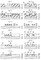
図1は、本発明のプローブユニットの製造方法の第1の実施形態の一例を示す断面模式図である。
この実施形態のプローブユニットの製造方法では、まず、図1(a)に示すように、基板1の表面上に、スパッタリング法、真空蒸着法、イオンプレーティング法などによって、犠牲膜2を形成する。本発明にあっては、スパッタリング法が好ましく用いられる。次に、犠牲膜2の表面上に、スパッタリング法によって、プローブユニットの下地となる下地膜3を形成する。
The present invention will be described in detail below.
FIG. 1 is a schematic cross-sectional view showing an example of a first embodiment of a method for manufacturing a probe unit according to the present invention.
In the probe unit manufacturing method of this embodiment, first, as shown in FIG. 1A, the
基板1としては、特に制限はないが、厚さ数mm程度のガラス板、合成樹脂板、セラミックス板、シリコン、金属板などが用いられる。
また、犠牲膜2としては、厚さ0.1〜5.0μm程度の銅薄膜、銅(Cu)/クロム(Cr)薄膜などが好ましい。特に、犠牲膜2として、銅/クロム薄膜が形成される場合、まず、クロムをスパッタリング法により形成して密着層とし、その上に銅をスパッタリング法により形成する。この場合のクロム薄膜の厚さは例えば0.03μm、銅薄膜の厚さは例えば0.3μm程度となっている。
Although there is no restriction | limiting in particular as the board |
The
下地膜3としては、厚さ0.05〜0.5μm程度のチタン(Ti)/ニッケル(Ni)−鉄(Fe)薄膜などが好ましい。下地膜3として、チタン/ニッケル−鉄薄膜が形成される場合、まず、チタン薄膜をスパッタリング法により形成して密着層とし、その上にニッケル−鉄薄膜をスパッタリング法により形成する。この場合のチタン薄膜の厚さは例えば0.02μm、ニッケル−鉄薄膜の厚さは例えば0.15μm程度となっている。
下地膜3は、犠牲膜2上に直接、後述のフォトレジストからなるレジスト膜を形成すると、高解像度のレジスト膜が得られないために用いられたものであり、フォトレジストの種類によっては不要である。下地膜3は、後述のフォトレジストとの濡れ性がよいから、下地膜3の存在により、犠牲膜2上に高解像度の任意形状のレジスト膜を形成することができる。
The
The
次に、図1(b)に示すように、下地膜3の表面上に、任意の厚さのフォトレジストを塗布し、このフォトレジストの表面に、任意形状のマスクを配置して、焼き付け、現像処理を行って不必要なフォトレジストを取り除き、任意のプローブユニットパターンの開口部を有するレジスト膜4を形成する。また、レジスト膜4の厚さは、10〜200μmとすることが好ましい。
このレジスト膜4の形成時には、プローブユニットを構成するプローブピンとプローブ保持部を形成するパターンを形成するだけでなく、プローブ保持部に、1個または複数個形成された後述の位置決め穴や位置決めフレームなどの位置決め部を形成するパターン、および後述の複数の細孔を形成するパターンを同時に形成することができる。
また、フォトレジストを用いてレジスト膜4を形成すれば、プローブピンを構成するリード群を形成するパターンを、狭小な間隔、例えば均一ピッチで互いに並列に形成することができるから、このレジスト膜4を用いて形成されるプローブピンは、狭小な間隔で互いに並列に形成されたリードを有するものとなる。また、同様に、このレジスト膜4を用いて形成されるプローブユニットは、高精度に、プローブピンとプローブ保持部とが位置決めされたものとなる。さらに、位置決め穴や細孔の位置決めも高精度に行うことができる。
Next, as shown in FIG. 1B, a photoresist having an arbitrary thickness is applied on the surface of the
When the resist film 4 is formed, not only a pattern for forming a probe pin and a probe holding part constituting the probe unit but also a positioning hole or a positioning frame, which will be described later, are formed in the probe holding part. A pattern for forming the positioning portion and a pattern for forming a plurality of pores to be described later can be formed simultaneously.
In addition, if the resist film 4 is formed using a photoresist, the patterns forming the lead groups constituting the probe pins can be formed in parallel with each other at a narrow interval, for example, a uniform pitch. The probe pins formed by using leads have leads formed in parallel with each other at a narrow interval. Similarly, the probe unit formed using the resist film 4 has the probe pin and the probe holding portion positioned with high accuracy. Furthermore, positioning holes and pores can be positioned with high accuracy.
次に、図1(c)に示すように、レジスト膜4の形成されていない下地膜3の表面上に、硫酸をベースとした公知の鉄、ニッケル用のメッキ液を用いて電気メッキをすることにより、メッキ成長させて、ニッケル合金などからなり、プローブユニットをなす金属箔5を形成する。このとき、金属箔5の厚さは、任意に設定できる。
Next, as shown in FIG. 1C, electroplating is performed on the surface of the
次に、図1(d)に示すように、レジスト膜4を除去する。レジスト膜4を除去するには、N−メチル−2−ピロリドンで、レジスト膜4と下地膜3の界面を洗浄する。このとき、基板1やレジスト膜4などからなる積層体を、N−メチル−2−ピロリドン中に浸漬し、85℃で、超音波洗浄すれば、レジスト膜4の除去を効率的に行うことができる。
Next, as shown in FIG. 1D, the resist film 4 is removed. In order to remove the resist film 4, the interface between the resist film 4 and the
次に、図1(e)に示すように、金属箔5の下層で、金属箔5よりも突出している部分の下地膜3を、イオンミリングによって除去し、下地膜3を金属箔5と同形状に形成する。
Next, as shown in FIG. 1 (e), the
次に、図1(f)に示すように、銅を優先的に溶解するエッチング液で犠牲膜2を溶解して、金属箔5と下地膜3を一体のまま基板1から剥離し、金属箔5と下地膜3とからなるプローブユニット6を得る。
Next, as shown in FIG. 1 (f), the
この実施形態のプローブユニットの製造方法にあっては、プローブピンとプローブ保持部を一体に形成するため、機械的に、またはハンダや接着剤などを用いて、プローブピンとプローブ保持部を接合する工程がないから、プローブピンが傷付くことがない。また、プローブピンとプローブ保持部とを、高精度に位置決めして接合することができる。
また、プローブ保持部を物理的に切り出す必要がないため、外形寸法の精度が高く、切り出した時に起きるプローブピンの破損のおそれもない。
In the probe unit manufacturing method of this embodiment, in order to integrally form the probe pin and the probe holding portion, there is a step of joining the probe pin and the probe holding portion mechanically or using solder or an adhesive. As a result, the probe pin is not damaged. In addition, the probe pin and the probe holding portion can be positioned and joined with high accuracy.
In addition, since it is not necessary to physically cut out the probe holding portion, the accuracy of the outer dimensions is high, and there is no possibility of damage to the probe pin that occurs when cutting out.
図2は、本発明のプローブユニットの製造方法の第1の実施形態で製造されたプローブユニットの一例を示す平面図である。
このプローブユニット6は、多数のリード7が高精度に狭小な間隔で互いに並列に配列されて櫛歯型をなすプローブピン8と、プローブピン8の一方の端部に垂直に接合するように形成されたプローブ保持部9とから構成され、これらが一体に形成されているものである。また、プローブピン8とプローブ保持部9とは同一平面上に存在している。さらに、プローブピン8とプローブ保持部9とは、メッキ成長により形成されたニッケル合金などの同一材質で形成されている。
この例のプローブユニットでは、プローブピン8とプローブ保持部9とが同一の金属からなるから、各リード7間には導通がある。したがって、この例のプローブユニットは、液晶パネルなどの同一部品から派生する複数の電極の通電試験を一度に行うプランジャタイプのプローブユニットとして好ましく用いられる。
FIG. 2 is a plan view showing an example of the probe unit manufactured in the first embodiment of the probe unit manufacturing method of the present invention.
The
In the probe unit of this example, since the
また、プローブ保持部9には、プローブユニット6を各種装置などに取り付ける際に位置決めをする位置決め穴10、10を形成してもよい。この位置決め穴10の大きさ、形状、位置などは、プローブユニット6が取り付けられる各種装置などに応じて適宜設定される。例えば、図2に示すような複数の丸穴に限らず、回転が防止できる角穴を1個または複数個設けてもよいし、取り付け位置が調整可能な長穴としてもよい。
また、この位置決め穴10は、上述のようにフォトレジストを用いて高精度に位置決めされているから、プローブユニット6を各種装置などに取り付ける際にも高精度に位置決めすることができる。したがって、液晶パネルなどの通電試験を高精度に行うことができる。
The probe holding part 9 may be formed with
Further, since the
また、プローブ保持部9には、多数の細孔11、11、…を形成してもよい。この細孔11は、本発明のプローブユニットの製造方法において、エッチング液で犠牲膜2を溶解して、金属箔5と下地膜3を一体のまま基板1から剥離する際に、エッチング液と犠牲膜2との接触面積を大きくするためのものである。したがって、細孔11の形成される位置や、細孔11の大きさや数は、特に限定されるものではないが、下地膜3の下層の犠牲膜2全体にまんべんなくエッチング液が接触するように形成されることが好ましい。このようにすれば、犠牲膜2の溶解時間が大幅に短縮される。
Moreover, you may form
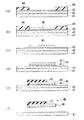
図3および図4は、本発明のプローブユニットの製造方法の第2の実施形態の一例を示す断面模式図である。図3(a−1)、・・・、(f−1)は、プローブユニットの長手方向に対して平行な断面の模式図である。図3(a−2)、・・・、(f−2)は、プローブユニットのプローブ保持部の位置決め穴の形成過程を示す断面模式図である。図4(a−1)、・・・、(f−1)は、プローブユニットの長手方向に対して平行な断面の模式図である。図4(a−2)、・・・、(f−2)は、プローブユニットのプローブ保持部の位置決め穴の形成過程を示す断面模式図である。
この実施形態のプローブユニットの製造方法では、まず、図3(a)に示すように、基板21の表面上に、スパッタリング法、真空蒸着法、イオンプレーティング法などによって、犠牲膜22を形成する。本発明にあっては、スパッタリング法が好ましく用いられる。次に、犠牲膜22の表面上に、任意の厚さのフォトレジストを塗布し、このフォトレジストの表面に、任意形状のマスクを配置して、焼き付け、現像処理を行って不必要なフォトレジストを取り除き、任意のプローブユニットのプローブ保持部のパターンを開口した第1のレジスト膜23を形成する。また、第1のレジスト膜23の厚さは、10〜200μmとすることが好ましい。次に、第1のレジスト膜23の形成されていない犠牲膜22の表面上に、硫酸をベースとした公知の鉄、ニッケル用のメッキ液を用いて電気メッキをすることにより、メッキ成長させて、ニッケル合金などからなり、プローブユニットのプローブ保持部をなす第1の金属箔24を形成する。このとき、第1の金属箔24の厚さは、任意に設定できる。
3 and 4 are cross-sectional schematic views showing an example of the second embodiment of the probe unit manufacturing method of the present invention. 3 (a-1),..., (F-1) are schematic views of cross sections parallel to the longitudinal direction of the probe unit. 3 (a-2),..., (F-2) is a schematic cross-sectional view illustrating a process of forming a positioning hole in the probe holding portion of the probe unit. 4 (a-1),..., (F-1) are schematic views of cross sections parallel to the longitudinal direction of the probe unit. 4 (a-2),..., (F-2) are schematic cross-sectional views showing the process of forming the positioning hole of the probe holding portion of the probe unit.
In the probe unit manufacturing method of this embodiment, first, as shown in FIG. 3A, a
基板21としては、特に制限はないが、厚さ数mm程度のガラス板、合成樹脂板、セラミックス板、シリコン、金属板などが用いられる。
また、犠牲膜22としては、厚さ0.1〜5μm程度の銅薄膜、銅(Cu)/クロム(Cr)薄膜などが好ましい。特に、犠牲膜22として、銅/クロム薄膜が形成される場合、まず、クロムをスパッタリング法により形成して密着層とし、その上に銅をスパッタリング法により形成する。この場合のクロム薄膜の厚さは例えば0.03μm、銅薄膜の厚さは例えば0.3μm程度となっている。
Although there is no restriction | limiting in particular as the board |
The
この第1のレジスト膜23の形成時には、プローブ保持部を形成するレジスト膜形状を形成するだけでなく、プローブ保持部に後述の1個または複数個の位置決め穴や細孔を形成する形状を同時に形成してもよい。
When the first resist
次に、図3(b)に示すように、第1のレジスト膜23および第1の金属箔24の表面上に、絶縁膜25を形成する。絶縁膜25は、スパッタリング法、CVD法などで形成された二酸化ケイ素膜、アルミナ膜などからなり、厚さ0.1〜20μm程度のものである。ところで、絶縁膜25は、第1の金属箔24の上に形成される後述のプローブピンと、第1の金属箔24を絶縁するために設けられたものである。
Next, as shown in FIG. 3B, an insulating
次に、図3(c)に示すように、第1のレジスト膜23を除去し、犠牲膜22の表面に上に、第1の金属箔24と絶縁膜25とからなるプローブ保持部26を得る。第1のレジスト膜23を除去するには、N−メチル−2−ピロリドンで、第1のレジスト膜23と犠牲膜22の界面を洗浄する。このとき、基板21や第1のレジスト膜23などからなる積層体を、N−メチル−2−ピロリドン中に浸漬し、85℃で、超音波洗浄すれば、第1のレジスト膜23の除去を効率的に行うことができる。
Next, as shown in FIG. 3 (c), the first resist
次に、図3(d)に示すように、犠牲膜22の第1のレジスト膜23が除去された後の部分、すなわち第1の金属箔24が形成されていない表面の全面に、電気メッキをすることにより、メッキ成長させて銅メッキを施し、銅メッキ層27を形成する。このとき、銅メッキ層27の厚さを、プローブ保持部26の厚さよりも大きくなるようにする。
次に、図3(e)に示すように、銅メッキ層27を、プローブ保持部26と共に研磨して、これらを面一とする。
Next, as shown in FIG. 3D, electroplating is performed on the portion of the
Next, as shown in FIG. 3E, the
次に、図3(f)に示すように、プローブ保持部26と銅メッキ層27の表面上に、スパッタリング法によって、プローブユニットの下地となる下地膜28を形成する。
下地膜28としては、厚さ0.05〜0.5μm程度のチタン(Ti)/ニッケル(Ni)−鉄(Fe)薄膜などが好ましい。下地膜28として、チタン/ニッケル−鉄薄膜が形成される場合、まず、チタン薄膜をスパッタリング法により形成して密着層とし、その上にニッケル−鉄薄膜をスパッタリング法により形成する。この場合のチタン薄膜の厚さは例えば0.02μm、ニッケル−鉄薄膜の厚さは例えば0.15μm程度となっている。
Next, as shown in FIG. 3F, a
The
次に、図4(a)に示すように、下地膜28の表面上に、任意の厚さのフォトレジストを塗布し、このフォトレジストの表面に、任意形状のマスクを配置して、焼き付け、現像処理を行って不必要なフォトレジストを取り除き、任意のプローブピンパターンを開口した第2のレジスト膜29を形成する。また、第2のレジスト膜29の厚さは、10〜200μmとすることが好ましい。また、プローブピンパターンに加えて、取り付け位置を決める位置決め部のパターンも同時に開口することができる。
Next, as shown in FIG. 4A, a photoresist having an arbitrary thickness is applied on the surface of the
次に、図4(b)に示すように、第2のレジスト膜29の形成されていない下地膜28の表面上に、硫酸をベースとした公知の鉄、ニッケル用のメッキ液を用いて電気メッキをすることにより、メッキ成長させて、ニッケル合金などからなり、プローブピンをなす第2の金属箔30を形成する。このとき、第2の金属箔30の厚さは、任意に設定できる。
Next, as shown in FIG. 4B, the surface of the
次に、図4(c)に示すように、第2のレジスト膜29を除去する。第2のレジスト膜29を除去するには、N−メチル−2−ピロリドンで、第2のレジスト膜29と下地膜28の界面を洗浄する。このとき、基板21や第2のレジスト膜29などからなる積層体を、N−メチル−2−ピロリドン中に浸漬し、85℃で、超音波洗浄すれば、第2のレジスト膜29の除去を効率的に行うことができる。
次に、図4(d)に示すように、第2の金属箔30の下層で、第2の金属箔30よりも突出している部分の下地膜28を、イオンミリングによって除去し、下地膜28を第2の金属箔30と同形状に形成し、プローブ保持部26の表面上に、下地膜28と第2の金属箔30とからなるプローブピン31を得る。
Next, as shown in FIG. 4C, the second resist
Next, as shown in FIG. 4D, the
次に、図4(e)に示すように、プローブ保持部26とプローブピン31との密着性を高め、プローブユニットの配線などを保護するために、プローブピン31がプローブ保持部26に密着している部分を保護膜32で覆う。この場合は、プローブピン31がプローブ保持部26に密着している部分に、感光性ポリイミドや紫外線硬化型接着剤、カルド型絶縁膜、フォトレジストなどを塗布、硬化するか、あるいは、ドライフィルムなどを貼付して保護膜32が形成される。
Next, as shown in FIG. 4E, in order to improve the adhesion between the
次に、図4(f)に示すように、銅を優先的に溶解するエッチング液で犠牲膜22と銅メッキ層27を溶解して、プローブピン31とプローブ保持部26を一体のまま基板21から剥離し、プローブピン31とプローブ保持部26とからなるプローブユニット33を得る。
Next, as shown in FIG. 4 (f), the
この実施形態のプローブユニットの製造方法にあっては、プローブピン31とプローブ保持部26を各種薄膜の積層により、一体に形成するため、機械的に、またはハンダや接着剤などを用いて、プローブピン31とプローブ保持部26を接合する工程がないから、プローブピン31が傷付くことがない。また、プローブピン31とプローブ保持部26とを、高精度に位置決めして接合することができる。
また、プローブ保持部26を物理的に切り出す必要がないため、外形寸法の精度が高く、切り出した時に起きるプローブピン31の破損のおそれもない。
また、上述のようにフォトレジストを用いて、プローブ保持部26に位置決め穴を形成した場合、これが高精度に位置決めされているから、プローブユニット33を各種装置などに取り付ける際にも高精度に位置決めすることができる。したがって、液晶パネルなどの通電試験を高精度に行うことができる。
また、取り付け位置を決める位置決め部のパターンと、プローブピン31とを同時に形成しているので、位置決め穴形成時の精度が高く、結果としてプローブピン31と被測定物との位置精度が向上する。
In the probe unit manufacturing method of this embodiment, since the
Further, since there is no need to physically cut out the
Further, when the positioning hole is formed in the
Further, since the positioning portion pattern for determining the attachment position and the
また、この例では保護膜32を形成したが、保護膜32を形成せずに、プローブユニット33を用いてもよい。あるいは、プローブユニット33を基板21から剥離した後、保護膜32を形成してもよい。
また、プローブユニット33を基板21から剥離する際の時間を短縮するために、基板21自体を銅で成形し、犠牲膜22を設けない方法を用いてもよい。この場合、銅製の基板21の強度が不足するようであれば、基板21に、ガラス、セラミックスなどからなる固く、安定した基板を裏打ちしてもよい。
また、この例ではプローブ保持部26を形成した後、これの上にプローブピン31を積層、形成したが、逆に、プローブピン31を形成した後、これの上にプローブ保持部26を積層、形成してもよい。
Further, although the
Further, in order to shorten the time when the
Further, in this example, after the
図5は、本発明のプローブユニットの製造方法の第2の実施形態で製造されたプローブユニットの一例を示し、図5(a)は平面図、図5(b)は、図5(a)のA―A´で切断した状態を示す断面図である。
このプローブユニット33は、プローブ保持部26と、多数のリード34、34、…が高精度に狭小な間隔で互いに並列に配列されて、その先端部分で櫛歯型をなすプローブピン31とを備え、プローブピン31がプローブ保持部26上に積層されて一体に形成されているものである。そして、このプローブユニット33には、多数の電極35、35、…が狭小な間隔で互いに並列に形成されたフレキシブルプリント基板36が、接合されている。プローブユニット33とフレキシブルプリント基板36との接合は、リード34と電極35が一対をなして接続するようになされる。
また、プローブ保持部26には、プローブユニット33を各種装置などに取り付ける際に位置決めをする位置決め穴37、37を形成してもよい。この位置決め穴37の大きさ、形状、位置などは、プローブユニット33が取り付けられる各種装置などに応じて適宜設定される。また、この位置決め穴37は、上述のようにフォトレジストを用いて高精度に位置決めされているから、プローブユニット33を各種装置などに取り付ける際にも高精度に位置決めすることができる。
また、位置決め穴37、37の表面の外周上には、プローブピン31の形成と同時に、プローブピン31と同じ材料で形成された位置決め部38、38を形成してもよい。この位置決め部38、38により、さらに位置決め精度を向上することができる。
FIG. 5 shows an example of a probe unit manufactured in the second embodiment of the probe unit manufacturing method of the present invention, FIG. 5 (a) is a plan view, and FIG. 5 (b) is FIG. 5 (a). It is sectional drawing which shows the state cut | disconnected by AA '.
The
Further, positioning holes 37 and 37 may be formed in the
Further, on the outer periphery of the surface of the positioning holes 37, 37,
図6は、本発明のプローブユニットの製造方法の第2の実施形態で製造されたプローブユニットの他の例を示す平面図である。
この例のプローブユニットでは、プローブ保持部26には、1個または複数個の細孔39、39、…を形成してもよい。この細孔39は、本発明のプローブユニットの製造方法において、エッチング液で犠牲膜22と銅メッキ層27を溶解して、プローブピン31とプローブ保持部26を一体のまま基板21から剥離する際に、エッチング液と犠牲膜22との接触面積を大きくするためのものである。したがって、細孔39の形成される位置や、細孔39の大きさや数は、特に限定されるものではなく、その形状はスリット状でもよいが、プローブ保持部26の下層の犠牲膜22全体にまんべんなくエッチング液が接触するように形成されることが好ましい。このようにすれば、犠牲膜22と銅メッキ層27の溶解時間が大幅に短縮される。
FIG. 6 is a plan view showing another example of the probe unit manufactured in the second embodiment of the probe unit manufacturing method of the present invention.
In the probe unit of this example, one or a plurality of
図7は、本発明のプローブユニットの製造方法の第3の実施形態の一例を示す断面模式図である。
この実施形態のプローブユニットの製造方法では、まず、図7(a)に示すように、基板41の表面上に、スパッタリング法、真空蒸着法、イオンプレーティング法などによって、犠牲膜42を形成する。本発明にあっては、スパッタリング法が好ましく用いられる。次に、犠牲膜42の表面上に、スパッタリング法によって、プローブユニットの下地となる下地膜43を形成する。次に、下地膜43の表面上に、任意の厚さのフォトレジストを塗布し、このフォトレジストの表面に、任意形状のマスクを配置して、焼き付け、現像処理を行って不必要なフォトレジストを取り除き、任意のプローブピンパターンを開口したレジスト膜44を形成する。
また、取り付け位置を決める位置決め部のパターンと、プローブピンパターンとを同時に形成することができるので、位置決め穴形成時の精度が高く、結果としてプローブピンと被測定物との位置精度が向上する。
FIG. 7 is a schematic cross-sectional view showing an example of the third embodiment of the method for manufacturing the probe unit of the present invention.
In the probe unit manufacturing method of this embodiment, first, as shown in FIG. 7A, the
In addition, since the positioning portion pattern for determining the attachment position and the probe pin pattern can be formed simultaneously, the accuracy in forming the positioning hole is high, and as a result, the positional accuracy between the probe pin and the object to be measured is improved.
基板41としては、特に制限はないが、厚さ数mm程度のガラス板、合成樹脂板、セラミックス板、シリコン、金属板などが用いられる。
また、犠牲膜42としては、厚さ0.1〜5μm程度の銅薄膜、銅(Cu)/クロム(Cr)薄膜などが好ましい。特に、犠牲膜42として、銅/クロム薄膜が形成される場合、まず、クロムをスパッタリング法により形成して密着層とし、その上に銅をスパッタリング法により形成する。この場合のクロム薄膜の厚さは例えば0.03μm、銅薄膜の厚さは例えば0.3μm程度となっている。
Although there is no restriction | limiting in particular as the board |
The
下地膜43としては、厚さ0.05〜0.5μm程度のチタン(Ti)/ニッケル(Ni)−鉄(Fe)薄膜などが好ましい。下地膜43として、チタン/ニッケル−鉄薄膜が形成される場合、まず、チタン薄膜をスパッタリング法により形成して密着層とし、その上にニッケル−鉄薄膜をスパッタリング法により形成する。この場合のチタン薄膜の厚さは例えば0.02μm、ニッケル−鉄薄膜の厚さは例えば0.15μm程度となっている。
ここで、下地膜43は、犠牲膜42上に直接、後述のフォトレジストからなるレジスト膜を形成すると、高解像度のレジスト膜が得られないために用いられたものである。下地膜43は、フォトレジストとの濡れ性がよいから、下地膜43の存在により、犠牲膜42上に高解像度の任意形状のレジスト膜を形成することができる。ただし、フォトレジストの種類によっては不要である。
The
Here, the
また、レジスト膜44の厚さは、10〜200μmとすることが好ましい。
このようにフォトレジストを用いてレジスト膜44を形成すれば、プローブピンを構成するリード群を狭小な間隔で互いに並列に形成することができる。また、プローブピンとプローブ保持部との位置決めを高精度に行うことができる。さらに、位置決め穴の位置決めも高精度に行うことができる。
The thickness of the resist
When the resist
次に、図7(b)に示すように、レジスト膜44の形成されていない下地膜43の表面上に、硫酸をベースとした公知の鉄、ニッケル用のメッキ液を用いて電気メッキをすることにより、メッキ成長させて、ニッケル合金などからなり、プローブピンをなす金属箔45を形成する。このとき、金属箔45の厚さは、任意に設定できる。
Next, as shown in FIG. 7B, electroplating is performed on the surface of the
次に、図7(c)に示すように、レジスト膜44を除去する。レジスト膜44を除去するには、N−メチル−2−ピロリドンで、レジスト膜44と下地膜43の界面を洗浄する。このとき、基板41やレジスト膜44などからなる積層体を、N−メチル−2−ピロリドン中に浸漬し、85℃で、超音波洗浄すれば、レジスト膜44の除去を効率的に行うことができる。
Next, as shown in FIG. 7C, the resist
次に、図7(d)に示すように、金属箔45の下層で、金属箔45よりも突出している部分の下地膜43を、イオンミリングによって除去し、下地膜43を金属箔45と同形状に形成し、犠牲膜42の表面上に、下地膜43と金属箔45とからなるプローブピン46を得る。
Next, as shown in FIG. 7 (d), the
次に、図7(e)に示すように、下地膜43と金属箔45が密着している部分に、感光性ポリイミドや紫外線硬化型接着剤、カルド型絶縁膜、フォトレジストなどを塗布、硬化するか、あるいは、ドライフィルムなどを貼付して、プローブ保持部47が形成されるが、好ましくは、フォトレジストが用いられる。この場合、プローブピン46を部分的に被覆するか、または、プローブピン46をプローブ保持部47で完全に被覆し、プローブピン46がプローブ保持部47内に埋め込まれた状態とする。このプローブ保持部47は、プローブピン46の保護膜としての役割も果たしている。
プローブ保持部47の形成に、フォトレジストを用いる場合、任意の厚さのフォトレジストをプローブピン46に塗布し、このフォトレジストの表面に、任意形状のマスクを配置して、焼き付け、現像処理を行って不必要なフォトレジストを取り除き、任意のプローブ保持部形状とする。また、この場合、プローブ保持部47の外形を形成するだけでなく、プローブ保持部47に、1個または複数個の位置決め穴や細孔を同時に形成することができる。
Next, as shown in FIG. 7E, photosensitive polyimide, an ultraviolet curable adhesive, a cardo type insulating film, a photoresist, or the like is applied and cured on the portion where the
When a photoresist is used to form the
次に、図7(f)に示すように、銅を優先的に溶解するエッチング液で犠牲膜42を溶解して、プローブピン46とプローブ保持部47を一体のまま基板41から剥離し、プローブピン46とプローブ保持部47とからなるプローブユニット48を得る。
Next, as shown in FIG. 7 (f), the
この実施形態のプローブユニットの製造方法にあっては、プローブピン46とプローブ保持部47を各種薄膜の積層により、一体に形成するため、機械的に、またはハンダや接着剤などを用いて、プローブピン46とプローブ保持部47を接合する工程がないから、プローブピン46が傷付くことがない。
また、プローブピン46とプローブ保持部47とを、高精度に位置決めして接合することができる。
また、上述のようにフォトレジストを用いて、プローブ保持部47を形成するため、位置決め穴を高精度に位置決めすることができるから、プローブユニット48を各種装置などに取り付ける際にも高精度に位置決めすることができる。したがって、液晶パネルなどの通電試験を高精度に行うことができる。
また、取り付け位置を決める位置決め部のパターンと、プローブピン46とを同時に形成することができるので、位置決め穴形成時の精度が高く、結果としてプローブピン46と被測定物との位置精度が向上する。
In the probe unit manufacturing method of this embodiment, since the
Further, the
Further, since the
Further, since the positioning portion pattern for determining the mounting position and the
また、プローブユニット48を基板41から剥離する際の時間を短縮するために、基板41自体を銅で成形し、犠牲膜42を設けない方法を用いてもよい。この場合、銅製の基板41の強度が不足するようであれば、基板41に、ガラス、セラミックスなどからなる固く、安定した基板を裏打ちしてもよい。
また、プローブ保持部47は樹脂からなるから、温度変化により、膨張、収縮し高い寸法精度が得られない場合がある。このような場合、図8に示すように、セラミックス、石英、シリコンなどの温度変化により、膨張、収縮し難い材料で形成されている保持板49を、プローブ保持部47に接着剤などで接着してもよい。
In order to shorten the time when the
In addition, since the
図9、図10および図11は、本発明のプローブユニットの製造方法の第4の実施形態の一例を示す断面模式図である。
この実施形態のプローブユニットの製造方法では、まず、図9(a)に示すように、基板51の表面上に、スパッタリング法、真空蒸着法、イオンプレーティング法などによって、犠牲膜52を形成する。本発明にあっては、スパッタリング法が好ましく用いられる。
基板51としては、特に制限はないが、厚さ数mm程度のガラス板、合成樹脂板、セラミックス板、シリコン、金属板などが用いられる。
また、犠牲膜52としては、厚さ0.1〜5μm程度の銅薄膜、銅(Cu)/クロム(Cr)薄膜などが好ましい。特に、犠牲膜52として、銅/クロム薄膜が形成される場合、まず、クロムをスパッタリング法により形成して密着層とし、その上に銅をスパッタリング法により形成する。この場合のクロム薄膜の厚さは例えば0.03μm、銅薄膜の厚さは例えば0.3μm程度となっている。
9, 10 and 11 are schematic cross-sectional views showing an example of the fourth embodiment of the method for manufacturing the probe unit of the present invention.
In the probe unit manufacturing method of this embodiment, first, as shown in FIG. 9A, a
Although there is no restriction | limiting in particular as the board |
The
次に、図9(b)に示すように、犠牲膜52の表面上に、スパッタリング法によって、プローブピンの下地となる第1の下地膜53を形成する。
第1の下地膜53としては、厚さ0.05〜0.5μm程度のチタン(Ti)/ニッケル(Ni)−鉄(Fe)薄膜などが好ましい。第1の下地膜53として、チタン/ニッケル−鉄薄膜が形成される場合、まず、チタン薄膜をスパッタリング法により形成して密着層とし、その上にニッケル−鉄薄膜をスパッタリング法により形成する。この場合のチタン薄膜の厚さは例えば0.02μm、ニッケル−鉄薄膜の厚さは例えば0.15μm程度となっている。
第1の下地膜53は、犠牲膜52上に直接、後述のフォトレジストからなるレジスト膜を形成すると、高解像度のレジスト膜が得られないために用いられたものであり、フォトレジストの種類によっては不要である。
Next, as shown in FIG. 9B, a
The
The
次に、図9(c)に示すように、第1の下地膜53の表面上に、任意の厚さのフォトレジストを塗布し、このフォトレジストの表面に、任意形状のマスクを配置して、焼き付け、現像処理を行って不必要なフォトレジストを取り除き、任意のプローブピンパターンを開口した第1のレジスト膜54を形成する。また、第1のレジスト膜54の厚さは、10〜200μmとすることが好ましい。
この第1のレジスト膜54の形成時には、プローブピンを形成するレジスト膜形状を形成するだけでなく、プローブユニットの位置決めをする1個または複数個のフレームのパターン、1個または複数個の位置決め穴や細孔を形成する形状を同時に形成してもよい。
Next, as shown in FIG. 9C, a photoresist having an arbitrary thickness is applied on the surface of the
When the first resist
次に、図9(d)に示すように、第1のレジスト膜54の形成されていない第1の下地膜53の表面上に、硫酸をベースとした公知の鉄、ニッケル用のメッキ液を用いて電気メッキをすることにより、メッキ成長させて、ニッケル合金などからなり、プローブピンおよび位置決め部をなす第1の金属箔55を形成する。このとき、第1の金属箔55の厚さは、任意に設定できる。
Next, as shown in FIG. 9D, a known iron or nickel plating solution based on sulfuric acid is applied on the surface of the
次に、図9(e)に示すように、第1のレジスト膜54を除去する。第1のレジスト膜54を除去するには、N−メチル−2−ピロリドンで、第1のレジスト膜54と第1の下地膜53の界面を洗浄する。このとき、基板51や第1のレジスト膜54などからなる積層体を、N−メチル−2−ピロリドン中に浸漬し、85℃で、超音波洗浄すれば、第1のレジスト膜54の除去を効率的に行うことができる。
Next, as shown in FIG. 9E, the first resist
次に、図9(f)に示すように、第1の金属箔55の下層で、第1の金属箔55よりも突出している部分の第1の下地膜53を、イオンミリングによって除去し、第1の下地膜53を第1の金属箔55と同形状に形成し、犠牲膜52の表面上に、第1の下地膜53と第1の金属箔55とからなるプローブピン56を得る。
Next, as shown in FIG. 9 (f), the portion of the
次に、図10(a)に示すように、犠牲膜52の表面およびプローブピン56の表面全面を、銅メッキ層57で覆う。このとき、銅メッキ層57を、犠牲膜52の表面およびプローブピン56の表面全面を完全に包囲するように、過剰に形成する。
次に、図10(b)に示すように、銅メッキ層57を、ダイヤモンドスラリなどを用いて研磨し、プローブピン56と面一にする。
Next, as shown in FIG. 10A, the surface of the
Next, as shown in FIG. 10B, the
次に、図10(c)に示すように、プローブピン56および銅メッキ層57の表面上に、絶縁膜58を形成する。絶縁膜58は、スパッタリング法、CVD法などで形成された二酸化ケイ素膜、アルミナ膜などからなり、厚さ0.1〜20μm程度のものである。ところで、絶縁膜58は、プローブピン56の上に形成される後述のプローブ保持部と、プローブピン56とを絶縁するために設けられたものである。
Next, as shown in FIG. 10C, an insulating
次に、図10(d)に示すように、絶縁膜58の表面上に、スパッタリング法によって、プローブ保持部の下地となる第2の下地膜59を形成する。
また、第2の下地膜59としては、第1の下地膜53と同様なものが用いられる。
Next, as shown in FIG. 10D, a
Further, as the
次に、図10(e)に示すように、第2の下地膜59の表面上に、任意の厚さのフォトレジストを塗布し、このフォトレジストの表面に、任意形状のマスクを配置して、焼き付け、現像処理を行って不必要なフォトレジストを取り除き、任意のプローブ保持部パターンを開口した第2のレジスト膜60を形成する。また、第2のレジスト膜60の厚さは、10〜200μmとすることが好ましい。また、プローブ保持部パターンに加えて、プローブユニットの位置決めをする1個または複数個のフレームのパターン、1個または複数個の位置決め穴や細孔を形成する形状を同時に開口することができる。
第2のレジスト膜60の形成に用いられるフォトレジストは、第1のレジスト膜54の形成に用いられたものと同様なものでよい。
Next, as shown in FIG. 10E, a photoresist having an arbitrary thickness is applied on the surface of the
The photoresist used for forming the second resist
次に、図11(a)に示すように、第2のレジスト膜60の形成されていない第2の下地膜59の表面上に、硫酸をベースとした公知の鉄、ニッケル用のメッキ液を用いて電気メッキをすることにより、メッキ成長させて、ニッケル合金などからなり、プローブ保持部をなす第2の金属箔61を形成する。このとき、第2の金属箔61の厚さは、任意に設定できる。
Next, as shown in FIG. 11A, a known iron or nickel plating solution based on sulfuric acid is applied on the surface of the
次に、図11(b)に示すように、第2のレジスト膜60を除去する。第2のレジスト膜60を除去するには、N−メチル−2−ピロリドンで、第2のレジスト膜60と第2の下地膜59の界面を洗浄する。このとき、基板51や第2のレジスト膜60などからなる積層体を、N−メチル−2−ピロリドン中に浸漬し、85℃で、超音波洗浄すれば、第2のレジスト膜60の除去を効率的に行うことができる。
Next, as shown in FIG. 11B, the second resist
次に、図11(c)に示すように、第2の金属箔61の下層で、第2の金属箔61よりも突出している部分の第2の下地膜59を、イオンミリングによって除去し、第2の下地膜59を第2の金属箔61と同形状に形成する。
Next, as shown in FIG. 11C, a portion of the
次に、図11(d)に示すように、第2の金属箔61の下層で、第2の金属箔61よりも突出している部分の絶縁膜58を、イオンエッチングによって除去し、絶縁膜58を第2の金属箔61と同形状に形成し、絶縁膜58と第2の金属箔61とからなるプローブ保持部62を得る。
次に、図11(e)に示すように、銅を優先的に溶解するエッチング液で犠牲膜52と銅メッキ層57を溶解して、プローブピン56とプローブ保持部62を一体のまま基板51から剥離し、プローブピン56とプローブ保持部62とからなるプローブユニット63を得る。
Next, as shown in FIG. 11D, the insulating
Next, as shown in FIG. 11E, the
この実施形態のプローブユニットの製造方法にあっては、プローブピン56とプローブ保持部62を各種薄膜の積層により、一体に形成するため、機械的に、またはハンダや接着剤などを用いて、プローブピン56とプローブ保持部62を接合する工程がないから、プローブピン56が傷付くことがない。
また、プローブピン56とプローブ保持部62とを、高精度に位置決めして接合することができる。
また、上述のようにフォトレジストを用いて、プローブピン56とプローブ保持部62を形成するため、位置決め用のフレーム、位置決め穴、細孔を高精度に位置決めすることができるから、プローブユニット63を各種装置などに取り付ける際にも高精度に位置決めすることができる。したがって、液晶パネルなどの通電試験を高精度に行うことができる。
また、フレーム、位置決め穴、細孔などの位置決め部のパターンと、プローブピン56とを同時に形成することができるので、位置決め部形成時の精度が高く、結果としてプローブピン56と被測定物との位置精度が向上する。
In the probe unit manufacturing method of this embodiment, the
Moreover, the
Further, since the
In addition, since the pattern of the positioning portion such as the frame, positioning hole, and fine hole and the
図12は、本発明のプローブユニットの製造方法の第3の実施形態で製造されたプローブユニットの一例を示し、図12(a)は平面図、図12(b)は断面模式図である。
このプローブユニット70は、プローブ保持部71と、多数のリード72、72、…が高精度に狭小な間隔で互いに並列に配列されて、その先端部分で櫛歯型をなすプローブピン73とから構成され、プローブピン73がプローブ保持部71上に積層されて一体に形成されているものである。そして、このプローブユニット70には、多数の電極74、74、…が狭小な間隔で互いに並列に形成されたフレキシブルプリント基板75が、接合されている。プローブユニット70とフレキシブルプリント基板75との接合は、リード72と電極74が一対をなして接続するようになされる。
FIG. 12 shows an example of the probe unit manufactured in the third embodiment of the probe unit manufacturing method of the present invention, FIG. 12 (a) is a plan view, and FIG. 12 (b) is a schematic cross-sectional view.
The
また、プローブ保持部71には、プローブユニット70を各種装置などに取り付ける際に位置決めをする位置決め穴76、76を形成してもよい。この位置決め穴76の大きさ、形状、位置などは、プローブユニット70が取り付けられる各種装置などに応じて適宜設定される。また、この位置決め穴76は、上述のようにフォトレジストを用いて高精度に位置決めされているから、プローブユニット70を各種装置などに取り付ける際にも高精度に位置決めすることができる。
また、位置決め穴76、76の表面の外周上には、プローブピン73の形成と同時に、プローブピン73と同じ材料で形成された位置決め部77、77が形成されている。
また、取り付け位置を決めるパターンと、プローブピンとを同時に形成しているので、位置決め穴の形成時の精度が高く、結果としてプローブピンと被測定物との位置精度が向上する。
Further, positioning holes 76 and 76 may be formed in the
Further, on the outer periphery of the surface of the positioning holes 76, 76,
Further, since the pattern for determining the attachment position and the probe pin are formed simultaneously, the accuracy in forming the positioning hole is high, and as a result, the positional accuracy between the probe pin and the object to be measured is improved.
図13は、本発明のプローブユニットの製造方法の第3の実施形態で製造されたプローブユニットの他の例を示す平面図である。
この例のプローブユニットでは、プローブ保持部71には、多数の細孔78、78、…を形成してもよい。この細孔78は、本発明のプローブユニットの製造方法において、エッチング液で犠牲膜を溶解して、プローブピン73とプローブ保持部71を一体のまま基板から剥離する際に、エッチング液と犠牲膜との接触面積を大きくするためのものである。したがって、細孔78の形成される位置や、その大きさおよび数は、特に限定されるものではないが、プローブ保持部71の下層の犠牲膜全体にまんべんなくエッチング液が接触するように形成されることが好ましい。このようにすれば、犠牲膜の溶解時間が大幅に短縮される。
FIG. 13: is a top view which shows the other example of the probe unit manufactured by 3rd Embodiment of the manufacturing method of the probe unit of this invention.
In the probe unit of this example, the
図14は、本発明のプローブユニットの製造方法の第3の実施形態で製造されたプローブユニットの第2の例を示す概略構成図であり、図14(a)は平面図、図14(b)は図14(a)のB―B´で切断した状態を示す断面図である。
この例のプローブユニットは、プローブ保持部81の一部が、樹脂層81aで形成されたものである。
この例のプローブユニットでは、プローブ保持部81とプローブピン83を絶縁するために、プローブ保持部81のプローブピン83が形成される部分を、レジスト、感光性ポリイミドなどの樹脂からなる樹脂層81aで形成した。樹脂層81aは線膨張率が大きく、温度変化により変形し、その結果としてプローブピンの位置精度が低下する。したがって、樹脂層81aがプローブ保持部81を占める割合が少ないことが好ましい。
この例のプローブユニットを、各種通電装置などに取り付ける際にも、通電装置のホルダ90の取り付け部91に、位置決めフレーム84を嵌合する。
FIG. 14 is a schematic configuration diagram showing a second example of the probe unit manufactured in the third embodiment of the probe unit manufacturing method of the present invention. FIG. 14 (a) is a plan view, and FIG. ) Is a cross-sectional view showing a state cut along BB 'in FIG.
In the probe unit of this example, a part of the
In the probe unit of this example, in order to insulate the
When the probe unit of this example is attached to various energization devices, the
図15は、本発明のプローブユニットの製造方法の第3の実施形態で製造されたプローブユニットの第3の例を示す概略構成図であり、図15(a)は平面図、図15(b)は図15(a)のC―C´で切断した状態を示す断面図である。
この例のプローブユニットは、位置決めフレーム84に、位置決め穴84aが形成されたものである。
この例のプローブユニットは、位置決めフレーム84および位置決め穴84aと、プローブピン83とが同時に形成されているので、位置決めフレーム84および位置決め穴84aの形成の精度が高くなり、結果としてプローブピン83と被測定物との位置精度が向上する。
この例のプローブユニットを、各種通電装置などに取り付ける際には、通電装置のホルダ92の位置決めピン93に、位置決め穴84aを嵌合する。
この例のプローブユニットでは、プローブ保持部81を占める樹脂層81aの割合が少ないから、温度変化によりプローブピンの位置精度が低下するのを防止することができる。また、位置決め穴84aの周辺に樹脂が使用されていないから、温度変化によりプローブピンの位置精度が低下するのを防止することができる。
FIG. 15 is a schematic configuration diagram showing a third example of the probe unit manufactured in the third embodiment of the probe unit manufacturing method of the present invention. FIG. 15A is a plan view, and FIG. ) Is a cross-sectional view showing a state cut along CC ′ in FIG.
In the probe unit of this example, a
In the probe unit of this example, since the
When the probe unit of this example is attached to various energization devices or the like, the
In the probe unit of this example, since the ratio of the
図16は、本発明のプローブユニットの製造方法の第4の実施形態で製造されたプローブユニットの第1の例を示す概略構成図であり、図16(a)は平面図、図16(b)は図16(a)のD―D´で切断した状態を示す断面図である。
この例のプローブユニットは、プローブ保持部81と、多数のリード82、82、…が高精度に狭小な間隔で互いに並列に配列されて、その先端部分で櫛歯型をなすプローブピン83と、位置決めフレーム84、84から概略構成されており、プローブピン83および位置決めフレーム84、84がプローブ保持部81上に積層されて一体に形成されているものである。
また、位置決めフレーム84、84は、プローブ保持部81の両端部に、リード82、82、…と平行に配置されている。また、位置決めフレーム84は、プローブピン83を形成する材料と同一のもので形成されている。この位置決めフレーム84の大きさ、形状、位置などは、この例のプローブユニットが取り付けられる各種通電装置などに応じて適宜設定される。
また、この例のプローブユニットは、取り付け位置を決める位置決めフレーム84と、プローブピン83とが同時に形成されているので、位置決めフレーム84の形成の精度が高くなり、結果としてプローブピン83と被測定物との位置精度が向上する。
この例のプローブユニットを、各種通電装置などに取り付ける際には、通電装置のホルダ90の取り付け部91に、位置決めフレーム84を嵌合する。
FIG. 16 is a schematic configuration diagram showing a first example of the probe unit manufactured in the fourth embodiment of the method for manufacturing the probe unit of the present invention. FIG. 16 (a) is a plan view, and FIG. ) Is a cross-sectional view showing a state cut along DD ′ in FIG.
The probe unit of this example includes a
Further, the positioning frames 84 and 84 are arranged at both ends of the
In the probe unit of this example, since the
When attaching the probe unit of this example to various energization devices, the
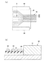
図17は、本発明のプローブユニットの製造方法で製造されたプローブユニットの使用例を示す正面模式図である。この図では、プローブユニットとして、図5に示したプローブユニット33を例示した。
プローブユニット33は、そのプローブ保持部26が、図示略の通電装置のホルダ100の接合面100aに接合され、フレキシブルプリント基板36の電極(図示略)を介して、通電装置の電気回路に接続されている。
また、プローブユニット33をホルダ100に接合するには、プローブ保持部26に形成された位置決め穴37を、ホルダ100の接合面に垂直に設けられた、先端にネジ溝が形成された位置決めピン101に嵌合し、ナットなどからなる固定金具102で固定する。
このプローブユニット33のプローブピン31の先端が、絶縁性材料で形成された試料台103に載置された液晶パネルなどの被測定物110の電極に押し当てられて、通電試験が行われる。
FIG. 17 is a schematic front view showing an example of use of the probe unit manufactured by the probe unit manufacturing method of the present invention. In this figure, the
The
Further, in order to join the
The tip of the
以上説明したように、本発明のプローブユニットの製造方法によれば、プローブピンとプローブ保持部が高精度に配置されかつ各種装置などへの取り付け用の穴が高精度に配置されたプローブユニットを製造することができる。したがって、液晶パネルなどの通電試験を高精度に行うことができる。また、取り付け位置を決めるパターンと、プローブピンとを同時に形成することができるので、位置決め穴形成時の精度が高く、結果としてプローブピンと被測定物との位置精度を向上することができる。 As described above, according to the probe unit manufacturing method of the present invention, a probe unit in which the probe pin and the probe holding portion are arranged with high accuracy and the holes for mounting to various devices and the like are arranged with high accuracy is manufactured. can do. Therefore, an energization test for a liquid crystal panel or the like can be performed with high accuracy. Further, since the pattern for determining the attachment position and the probe pin can be formed simultaneously, the accuracy in forming the positioning hole is high, and as a result, the positional accuracy between the probe pin and the object to be measured can be improved.
また、本発明のプローブユニットは、プローブピンと、プローブ保持部とを備えたプローブユニットであって、前記プローブ保持部には1または複数の位置決め部が形成されたものであるから、このプローブユニットを各種装置などに取り付ける際に、高精度に位置決めすることができる。
前記プローブ保持部に複数の細孔が形成されていれば、このプローブユニットをエッチングする際に効率が高くなる。
前記プローブ保持部が、レジストで形成されたフレーム内にメッキにより形成されたものであれば、プローブ保持部の厚さは均一であり、また、プローブ保持部に形成されている位置決め穴や位置決めフレームなどの位置決め部、および細孔が高精度に配置されている。
メッキで形成されたプローブ保持部の表面に絶縁膜が形成され、該絶縁膜の表面にプローブピンが形成されていれば、絶縁膜上に、フォトレジストを用いてプローブピンパターンを形成する際に、高解像度のプローブピンパターンが形成されるから、得られたプローブピンは高精度となっている。
前記プローブ保持部および前記プローブピンが保護膜で覆われていれば、プローブ保持部とプローブピンとの密着性を高めることができ、また、プローブユニットの配線などを保護することができる。
メッキで形成されたプローブ保持部の表面に、該プローブ保持部と同じ材料、または、ほぼ同じ材料、例えば、合金系が同一である材料などからなるプローブピンが形成されていれば、プローブ保持部とプローブピンとの密着性が高くなり、プローブ保持部とプローブピンとが高精度に配置される。
メッキで形成されたプローブピンが、樹脂で形成されたプローブ保持部内に埋め込まれていれば、プローブピンとプローブ保持部が一体に形成されるから、プローブピンが傷付くことがない。また、プローブピンとプローブ保持部とが、高精度に位置決めされて、接合される。
Further, the probe unit of the present invention is a probe unit including a probe pin and a probe holding part, and the probe holding part is formed with one or a plurality of positioning parts. When attaching to various devices, it can be positioned with high accuracy.
If a plurality of pores are formed in the probe holding part, the efficiency becomes higher when the probe unit is etched.
If the probe holding part is formed by plating in a frame made of resist, the thickness of the probe holding part is uniform, and positioning holes and positioning frames formed in the probe holding part The positioning part and the like and the fine holes are arranged with high accuracy.
When an insulating film is formed on the surface of the probe holding portion formed by plating and a probe pin is formed on the surface of the insulating film, a probe pin pattern is formed on the insulating film using a photoresist. Since the high-resolution probe pin pattern is formed, the obtained probe pin has high accuracy.
If the probe holding part and the probe pin are covered with a protective film, the adhesion between the probe holding part and the probe pin can be improved, and the wiring of the probe unit can be protected.
If a probe pin made of the same material as or substantially the same material as the probe holding part, for example, a material having the same alloy system, is formed on the surface of the probe holding part formed by plating, the probe holding part The probe holding portion and the probe pin are arranged with high accuracy.
If the probe pin formed by plating is embedded in the probe holding portion made of resin, the probe pin and the probe holding portion are integrally formed, so that the probe pin is not damaged. Further, the probe pin and the probe holding part are positioned and joined with high accuracy.
1,21,41,51・・・基板、2,22,42,52・・・犠牲膜、3,28,43・・・下地膜、4,44・・・レジスト膜、5,45・・・金属箔、6,33,48,63,70・・・プローブユニット、7,34,72,82・・・リード、8,31,46,56,73,83・・・プローブピン、9,26,47,62,71,81・・・プローブ保持部、10,37,76,84a・・・位置決め穴、11,39,78・・・細孔、23,54・・・第1のレジスト膜、24・・・第1の金属箔、25,58・・・絶縁膜、27,57・・・銅メッキ層、29,60・・・第2のレジスト膜、30・・・第2の金属箔、32・・・保護膜、35,74・・・電極、36,75・・・フレキシブルプリント基板、38,77・・・位置決め部、49・・・保持板、53・・・第1の下地膜、55・・・第1の金属箔、59・・・第2の下地膜、61・・・第2の金属箔、81a・・・樹脂層、84・・・位置決めフレーム、90,92,100・・・ホルダ、91・・・取り付け部、93,101・・・位置決めピン、100a・・・接合面、102・・・固定金具、103・・・試料台、110・・・被測定物 1, 21, 41, 51 ... substrate, 2, 22, 42, 52 ... sacrificial film, 3, 28, 43 ... base film, 4, 44 ... resist film, 5, 45 ... -Metal foil, 6, 33, 48, 63, 70 ... Probe unit, 7, 34, 72, 82 ... Lead, 8, 31, 46, 56, 73, 83 ... Probe pin, 9, 26, 47, 62, 71, 81... Probe holding portion, 10, 37, 76, 84a... Positioning hole, 11, 39, 78... Pore, 23, 54. Film, 24 ... first metal foil, 25,58 ... insulating film, 27,57 ... copper plating layer, 29,60 ... second resist film, 30 ... second Metal foil, 32 ... protective film, 35, 74 ... electrode, 36, 75 ... flexible printed circuit board, 38, 77 ... Positioning part, 49 ... holding plate, 53 ... first base film, 55 ... first metal foil, 59 ... second base film, 61 ... second metal foil, 81a ... resin layer, 84 ... positioning frame, 90, 92, 100 ... holder, 91 ... mounting portion, 93, 101 ... positioning pin, 100a ... joining surface, 102 ...・ Fixing bracket, 103 ... Sample stand, 110 ... Measurement object
Claims (5)
The method of manufacturing a probe unit according to any one of claims 1 to 4, wherein the positioning portion that determines the attachment position of the probe unit and the probe pin are made of the same material.
Priority Applications (1)
| Application Number | Priority Date | Filing Date | Title |
|---|---|---|---|
| JP2004374733A JP4074287B2 (en) | 2001-09-20 | 2004-12-24 | Manufacturing method of probe unit |
Applications Claiming Priority (2)
| Application Number | Priority Date | Filing Date | Title |
|---|---|---|---|
| JP2001287088 | 2001-09-20 | ||
| JP2004374733A JP4074287B2 (en) | 2001-09-20 | 2004-12-24 | Manufacturing method of probe unit |
Related Parent Applications (1)
| Application Number | Title | Priority Date | Filing Date |
|---|---|---|---|
| JP2002164244A Division JP3651451B2 (en) | 2001-09-20 | 2002-06-05 | Probe unit and manufacturing method thereof |
Publications (3)
| Publication Number | Publication Date |
|---|---|
| JP2005099052A JP2005099052A (en) | 2005-04-14 |
| JP2005099052A5 JP2005099052A5 (en) | 2007-02-01 |
| JP4074287B2 true JP4074287B2 (en) | 2008-04-09 |
Family
ID=34466581
Family Applications (1)
| Application Number | Title | Priority Date | Filing Date |
|---|---|---|---|
| JP2004374733A Expired - Fee Related JP4074287B2 (en) | 2001-09-20 | 2004-12-24 | Manufacturing method of probe unit |
Country Status (1)
| Country | Link |
|---|---|
| JP (1) | JP4074287B2 (en) |
Cited By (1)
| Publication number | Priority date | Publication date | Assignee | Title |
|---|---|---|---|---|
| KR20220148688A (en) * | 2021-04-29 | 2022-11-07 | (주)샘씨엔에스 | Method for impedance matching of space transformer for probe card |
Families Citing this family (1)
| Publication number | Priority date | Publication date | Assignee | Title |
|---|---|---|---|---|
| JP4584972B2 (en) * | 2007-10-17 | 2010-11-24 | 山一電機株式会社 | Probe contact manufacturing method and probe contact |
-
2004
- 2004-12-24 JP JP2004374733A patent/JP4074287B2/en not_active Expired - Fee Related
Cited By (2)
| Publication number | Priority date | Publication date | Assignee | Title |
|---|---|---|---|---|
| KR20220148688A (en) * | 2021-04-29 | 2022-11-07 | (주)샘씨엔에스 | Method for impedance matching of space transformer for probe card |
| KR102594037B1 (en) | 2021-04-29 | 2023-10-25 | (주)샘씨엔에스 | Method for impedance matching of space transformer for probe card |
Also Published As
| Publication number | Publication date |
|---|---|
| JP2005099052A (en) | 2005-04-14 |
Similar Documents
| Publication | Publication Date | Title |
|---|---|---|
| JP3123483B2 (en) | Probe card and probe card forming method | |
| US7087501B2 (en) | Manufacture of probe unit having lead probes extending beyond edge of substrate | |
| KR100306412B1 (en) | Bump structure, anisotropic conductive film, and method for making the bump structure | |
| JP2004259530A (en) | Semiconductor device with exterior contact terminal and its using method | |
| JP2007285801A (en) | Probe sheet and electrical connection apparatus | |
| JP2023081264A (en) | Multilayer wiring board manufacturing method | |
| US4200975A (en) | Additive method of forming circuit crossovers | |
| JP4074287B2 (en) | Manufacturing method of probe unit | |
| JP3651451B2 (en) | Probe unit and manufacturing method thereof | |
| KR100684677B1 (en) | Probe unit and its manufacture | |
| JP2008004862A (en) | Printed circuit board and method for manufacturing it | |
| JP4160665B2 (en) | Contact board and its components | |
| JP5643477B2 (en) | Contact probe | |
| JP4803608B2 (en) | Contact board and its components | |
| JP5058032B2 (en) | Contact probe manufacturing method | |
| JP2006038457A (en) | Film probe manufacturing method | |
| JP2004069485A (en) | Probe unit, its manufacturing method, probe card, and its manufacturing method | |
| KR200405297Y1 (en) | Probe unit | |
| JP4074297B2 (en) | Manufacturing method of probe unit | |
| JP2003207521A (en) | Probe unit, manufacturing method thereof, and energization inspection device | |
| JP2003121466A (en) | Probe unit and its manufacturing method | |
| JP2000304772A (en) | Terminal device for inspection and its manufacture | |
| JP2010107319A (en) | Manufacturing method of contact probe | |
| JP3449997B2 (en) | Semiconductor device test method and test board | |
| JP2014016371A (en) | Contact probe |
Legal Events
| Date | Code | Title | Description |
|---|---|---|---|
| A521 | Written amendment |
Free format text: JAPANESE INTERMEDIATE CODE: A523 Effective date: 20050121 |
|
| A621 | Written request for application examination |
Free format text: JAPANESE INTERMEDIATE CODE: A621 Effective date: 20050224 |
|
| RD04 | Notification of resignation of power of attorney |
Free format text: JAPANESE INTERMEDIATE CODE: A7424 Effective date: 20060727 |
|
| RD01 | Notification of change of attorney |
Free format text: JAPANESE INTERMEDIATE CODE: A7426 Effective date: 20061107 |
|
| RD03 | Notification of appointment of power of attorney |
Free format text: JAPANESE INTERMEDIATE CODE: A7423 Effective date: 20061107 |
|
| A521 | Written amendment |
Free format text: JAPANESE INTERMEDIATE CODE: A523 Effective date: 20061123 |
|
| A521 | Written amendment |
Free format text: JAPANESE INTERMEDIATE CODE: A821 Effective date: 20061107 |
|
| A711 | Notification of change in applicant |
Free format text: JAPANESE INTERMEDIATE CODE: A711 Effective date: 20061213 |
|
| RD03 | Notification of appointment of power of attorney |
Free format text: JAPANESE INTERMEDIATE CODE: A7423 Effective date: 20061213 |
|
| A131 | Notification of reasons for refusal |
Free format text: JAPANESE INTERMEDIATE CODE: A131 Effective date: 20070405 |
|
| A521 | Written amendment |
Free format text: JAPANESE INTERMEDIATE CODE: A523 Effective date: 20070601 |
|
| TRDD | Decision of grant or rejection written | ||
| A01 | Written decision to grant a patent or to grant a registration (utility model) |
Free format text: JAPANESE INTERMEDIATE CODE: A01 Effective date: 20080108 |
|
| A61 | First payment of annual fees (during grant procedure) |
Free format text: JAPANESE INTERMEDIATE CODE: A61 Effective date: 20080124 |
|
| FPAY | Renewal fee payment (event date is renewal date of database) |
Free format text: PAYMENT UNTIL: 20110201 Year of fee payment: 3 |
|
| R150 | Certificate of patent or registration of utility model |
Free format text: JAPANESE INTERMEDIATE CODE: R150 |
|
| FPAY | Renewal fee payment (event date is renewal date of database) |
Free format text: PAYMENT UNTIL: 20110201 Year of fee payment: 3 |
|
| FPAY | Renewal fee payment (event date is renewal date of database) |
Free format text: PAYMENT UNTIL: 20120201 Year of fee payment: 4 |
|
| FPAY | Renewal fee payment (event date is renewal date of database) |
Free format text: PAYMENT UNTIL: 20120201 Year of fee payment: 4 |
|
| FPAY | Renewal fee payment (event date is renewal date of database) |
Free format text: PAYMENT UNTIL: 20130201 Year of fee payment: 5 |
|
| FPAY | Renewal fee payment (event date is renewal date of database) |
Free format text: PAYMENT UNTIL: 20130201 Year of fee payment: 5 |
|
| FPAY | Renewal fee payment (event date is renewal date of database) |
Free format text: PAYMENT UNTIL: 20130201 Year of fee payment: 5 |
|
| FPAY | Renewal fee payment (event date is renewal date of database) |
Free format text: PAYMENT UNTIL: 20130201 Year of fee payment: 5 |
|
| FPAY | Renewal fee payment (event date is renewal date of database) |
Free format text: PAYMENT UNTIL: 20140201 Year of fee payment: 6 |
|
| R250 | Receipt of annual fees |
Free format text: JAPANESE INTERMEDIATE CODE: R250 |
|
| LAPS | Cancellation because of no payment of annual fees |