JP4065601B2 - Low noise switching regulator and method for controlling a switching regulator - Google Patents
Low noise switching regulator and method for controlling a switching regulator Download PDFInfo
- Publication number
- JP4065601B2 JP4065601B2 JP11573798A JP11573798A JP4065601B2 JP 4065601 B2 JP4065601 B2 JP 4065601B2 JP 11573798 A JP11573798 A JP 11573798A JP 11573798 A JP11573798 A JP 11573798A JP 4065601 B2 JP4065601 B2 JP 4065601B2
- Authority
- JP
- Japan
- Prior art keywords
- output
- current
- voltage
- node
- switching regulator
- Prior art date
- Legal status (The legal status is an assumption and is not a legal conclusion. Google has not performed a legal analysis and makes no representation as to the accuracy of the status listed.)
- Expired - Lifetime
Links
Images


Classifications
-
- H—ELECTRICITY
- H03—ELECTRONIC CIRCUITRY
- H03K—PULSE TECHNIQUE
- H03K17/00—Electronic switching or gating, i.e. not by contact-making and –breaking
- H03K17/08—Modifications for protecting switching circuit against overcurrent or overvoltage
- H03K17/082—Modifications for protecting switching circuit against overcurrent or overvoltage by feedback from the output to the control circuit
- H03K17/0826—Modifications for protecting switching circuit against overcurrent or overvoltage by feedback from the output to the control circuit in bipolar transistor switches
-
- H—ELECTRICITY
- H03—ELECTRONIC CIRCUITRY
- H03K—PULSE TECHNIQUE
- H03K17/00—Electronic switching or gating, i.e. not by contact-making and –breaking
- H03K17/16—Modifications for eliminating interference voltages or currents
-
- H—ELECTRICITY
- H02—GENERATION; CONVERSION OR DISTRIBUTION OF ELECTRIC POWER
- H02M—APPARATUS FOR CONVERSION BETWEEN AC AND AC, BETWEEN AC AND DC, OR BETWEEN DC AND DC, AND FOR USE WITH MAINS OR SIMILAR POWER SUPPLY SYSTEMS; CONVERSION OF DC OR AC INPUT POWER INTO SURGE OUTPUT POWER; CONTROL OR REGULATION THEREOF
- H02M1/00—Details of apparatus for conversion
- H02M1/0003—Details of control, feedback or regulation circuits
- H02M1/0029—Circuits or arrangements for limiting the slope of switching signals, e.g. slew rate
Description
【0001】
【発明の属する技術分野】
本発明は、波形整形を用いて、誘導性負荷を切り換える(「駆動する」とも言う)ことにより生じる高周波数雑音を低減する装置およびその方法に関する。具体的には、本発明は、電流スルー制御および電圧スルー制御を用いて、誘導性負荷を切り換えることにより生じる高周波数雑音を低減する装置およびその方法に関する。ここで、「スルー」とは、波形の傾き(あるいは、変化率)を指す。
【0002】
【従来の技術】
電気製品の設計においてますます重要になっている問題は、高周波数電磁雑音である。この雑音は、製品の性能を低減させるかあるいは他の製品の妨害を引き起こす可能性がある。この雑音源を解消し、雑音の影響を低減する試みには、膨大なエネルギーおよびコストが費やされている。例えばモータ、ソレノイド、およびスイッチングレギュレータなどの電気装置においてスイッチング電流およびスイッチング電圧は、遍在する雑音源である。携帯電話などの新しい製品では、適切に動作させるために、さらに低レベルの伝導電磁雑音および放射電磁雑音が必要である。電磁汚染の抑制に関する法律も増えている。ヨーロッパ放出/磁化率規格はその適例である。
【0003】
【発明が解決しようとする課題】
波形の急激な遷移には、より多くの高周波数成分が含まれる。これについては、フーリエ級数およびフーリエ変換により数学的に示すことができる。例えば、純粋な正弦波は1つの周波数成分を有し、方形波はより多くの高周波数成分を有し、その振幅は周波数とともに減少する。高周波の含有量の低減は、遷移の鋭さの低減を意味する。
【0004】
図1Aおよび図1Bは、高周波数成分に関する単純な親指の法則を示す。方形波では、高周波成分の大きさは以下に示す基本周波数から20dB/DECADEのレートで減少する。
【0005】
【数1】

ここで、「on−time」は、スイッチが電流を伝導する時間である。
【0007】
スルーエッジを有する波形は、ほぼ一定の傾きの遷移を有する波形、即ち、ランプ信号である。これは、波形の第一次導関数が制御されることを意味する。スルーエッジを有する波形はしばしば、丸い角部を有している。スルーエッジと一定の第一次導関数とを有する波形では、高周波数成分は、基本周波数から20dB/DECADEでロールオフし、以下の式に等しい周波数から40dB/DECADEでロールオフする。
【0008】
【数2】
ここで、tslewは、スルーエッジの遷移時間である。
【0010】
電気装置からの放射は、通常、電界あるいは磁界のいずれかの支配的な電磁界に関して考えることができる。電界および磁界のいずれであっても、回路に雑音を引き起こし得る。電界放射は、電圧の変化によって生じる。磁界放射は、電流の変化によって生じる。その対策を行う場合、放射源を低減し且つそれを受け取る回路を遮蔽することが多い。
【0011】
電界によって生じる雑音の低減は、コンデンサのような素子で電圧遷移を低速化することによって達成することができる。結合容量を低減することにより、受信端での雑音強度を低下させることができる。このような結合容量の低下は、構成要素、配線、およびプリント回路板トレースのための金属の囲いおよび金属のシールドにより行われる。
【0012】
磁界によって生じる雑音を含む場合はさらに困難である。雑音源の強度を低減する場合、電流遷移を低速化する必要がある。この低速化はしばしば、容量性素子よりも通常高価である誘導性素子を加えることにより行われる。磁界によって生じる雑音から、それを受け取る素子を遮蔽するには、特殊なシールドが必要であり、このシールドとしては、高価なミューメタルシールドがしばしば用いられる。磁界によって生じる雑音により、付近のプリント回路板トレースにおいて電流が生成され得るため、完全なシールドを与えることはしばしば困難である。
【0013】
スイッチングレギュレータトポロジーには、高周波数フィルタ素子を、コスト削減に役立ち得る電力構成要素に組み込むものもある。しかし、そのようなトポロジーであっても、依然として、放出を減らすために特定の構成要素を加えることが多い。
【0014】
外部構成要素を加えると必然的にシステムコストが増大する。従って、加える外部構成要素の数を最小限にすることが望ましい。そのような外部構成要素を加えるのは、通常、電流および/または電圧の変化レートを低くするためである。これは、高周波数成分が形成された(フィルタを加えた)後にそれらの高周波成分を分流するか、あるいは、高周波成分の形成を最小にすることによって行うことができる。しかし、それに関連して、フィルタリングによる電力損失が起こる。この電力損失は、電流が大きいために起こることが多い。
【0015】
インダクタの電圧スルー(dv/dt)の制御は、フィルタを形成することによって行われることもある。切換ノードに容量を加えると、電圧遷移が低速化され、高周波成分が吸収される。しかし、必要とされる高電流のため、コンデンサは、物理的に大きくなる場合があり、相当量の電力を放散する可能性がある。これにより、切換効率が低下する。
【0016】
スイッチングレギュレータは、その変換効率のため、非常に望ましい。しかし、この変換効率は、より多くの高周波数電磁波が含まれる電流および電圧波形を作るという犠牲を払って得られるものである。この高周波数雑音は、伝導あるいは放射電磁結合(容量性および誘導性)により、付近の回路に結合する。スイッチングレギュレータの設計者はしばしば、効率と、雑音と、性能との間で妥協を強いられる。
【0017】
スイッチングレギュレータでは、電磁妨害のほとんどは、以下の4つの要因により発生する。(1)インダクタの電流が急激に変化し、これにより高周波数磁気雑音が形成され、付近の線に変化を引き起こす;(2)インダクタ電流が変化し、これにより、デカップリングコンデンサの等価直列抵抗(「ESR」)および等価直列インダクタンス(「ESL」)のために電圧が突然変化する;(3)接地に容量結合する出力スイッチング素子において電圧が突然変化し、これにより、電力線に過渡電流を引き起こす;(4)ダイオードがオフになると、急激な電流の過渡現象が生じるとともに、高周波数磁気雑音が生成され、さらに、コンデンサESRを介して高周波数電圧の過渡現象が生成され得る。
【0018】
妨害となる雑音は、電力配線および接地配線における伝導と、「高温」構成要素から他の回路への容量結合または電磁放射結合とにより、他の回路にも導入される。典型的には、伝導雑音は低周波数に関してより問題が多く、放射雑音は高周波数に関してより問題が多い。スイッチングレギュレータの場合、インダクタまたは変圧器の電流およびスイッチング素子の電流は、最も大きい電流であるため、通常、最も面倒な雑音源である。同様に、スイッチングレギュレータのスイッチにおける電圧動作範囲(excursion)はしばしば、その遷移速度および電力経路への接続のため、最大の雑音源である。
【0019】
以上のことに鑑みて、回路性能を犠牲にすることなく、あるいは、別の構成要素を加えることなく、誘導性負荷を切り換えることによって生じる高周波数雑音成分を低減する装置およびその方法を提供することが望ましいであろう。
【0020】
高調波含有量と変換効率との間のトレードオフについてさらなる制御を可能にすることも望ましいであろう。
【0021】
【課題を解決するための手段】
本発明による低ノイズスイッチングレギュレータは、誘導負荷を駆動する低ノイズスイッチングレギュレータであって、電流および電圧スルー信号に応答する制御回路機構を含み、このことにより上記目的が達成される。
【0022】
前記スイッチングレギュレータが、前記負荷に接続されたドライバと、該ドライバに接続された電流スルー制御フィードバックループと、該負荷に接続された電圧スルー制御フィードバックループと、を含んでもよい。
【0023】
1以上の正の整数MおよびNに関して、前記電圧スルー制御フィードバックループが、前記負荷の電圧の第1次から第M次の1つ以上の導関数の合計に比例する第1のフィードバック信号を生成し、そして前記電流スルー制御フィードバックループが、該負荷を通る電流の第1次から第N次の1つ以上の導関数の合計に比例する第2のフィードバック信号を生成してもよい。
【0024】
駆動電圧、前記電流スルー制御フィードバックループの出力、および前記電圧スルー制御フィードバックループの出力が合計されて、前記ドライバへの入力を形成してもよい。
【0025】
前記負荷が、信号ノードと出力ノードとの間に接続され、前記電流スルー制御フィードバックループの入力が、該信号ノードに接続され、そして前記電圧スルー制御フィードバックループの入力が、該出力ノードに接続されてもよい。
【0026】
前記ドライバが、駆動増幅器を含んでもよい。
【0027】
前記電圧スルー制御フィードバックループが、微分増幅器を含んでもよい。
【0028】
前記電流スルー制御フィードバックループが、抵抗器を介して前記信号ノードに接続されるセンス増幅器と、該センス増幅器に接続される微分増幅器とを含んでもよい。
【0029】
前記駆動電圧の振幅の絶対値が、第1の値に制限され、前記微分増幅器の出力の絶対値が、第2の値に制限され、該微分増幅器の該出力が、第3の値によって乗算され、該第3の値は、該第2の値によって除算された該第1の値に等しくてもよい。
【0030】
電圧スルー制御が、前記負荷を通る電流の第二次導関数を制御することにより達成されてもよい。
【0031】
前記スイッチングレギュレータが、前記負荷に接続されたドライバと、該負荷に接続された電流スルー制御フィードバックループと、該電流スルー制御フィードバックループの出力に接続され、該出力と組み合わせられる、第二次導関数ループと、を備えてもよい。
【0032】
前記スイッチングレギュレータが、開ループ制御システムを含んでもよい。
【0033】
本発明による低ノイズスイッチングレギュレータは、低ノイズスイッチングレギュレータ誘導負荷を駆動する低ノイズスイッチングレギュレータであって、該負荷に接続されたスイッチ入力端子と、スイッチ出力端子とを有するスイッチを備えたドライバと、該スイッチ出力端子に接続された電流スルー制御フィードバックループと、該スイッチ出力端子に接続された電圧スルー制御ループとを含み、このことにより、上記目的が達成される。
【0034】
前記スイッチが、スイッチ制御端子をさらに含み、前記ドライバが、駆動ノードと該スイッチ制御端子との間に直列で接続されたバッファ増幅器をさらに含み、前記電流スルー制御フィードバックループが:前記スイッチ出力端子と接地との間に接続された抵抗器と;該スイッチ出力端子に接続された第1の入力と、接地に接続された第2の入力とを有するセンス増幅器と;該センス増幅器の出力と、電流スルー制御フィードバックノードとの間に接続された第1のコンデンサと;該電流スルー制御フィードバックノードに接続された負の入力と、参照電位の電源に接続された正の入力と、該電流スルー制御フィードバックノードに接続された出力とを有する第1のトランスコンダクタンス増幅器と;該電流スルー制御フィードバックノードに接続された第1の入力と、参照電位の該電源に接続された第2の入力と、該駆動ノードに接続された出力とを有する第2のトランスコンダクタンス増幅器と;を備え、前記電圧スルー制御ループが、前記負荷と該駆動ノードとの間に接続された第2のコンデンサを備えてもよい。
【0035】
駆動電圧の電源に接続された第1の入力と、参照電位の前記電源に接続された第2の入力と、前記駆動ノードに接続された出力とを有する第3のトランスコンダクタンス増幅器をさらに備えてもよい。
【0036】
本発明による低ノイズスイッチングレギュレータは、信号ノードと出力ノードとの間に接続された誘導負荷を駆動するための低ノイズスイッチングレギュレータであって、駆動ノードと、第1の加算器入力と、第2の加算器入力と、第3の加算器入力と、加算器出力とを有する加算器と、該駆動ノードと該第1の加算器入力との間に接続された第1の制限器と、該第3の加算器入力に接続された出力を有する乗算器と、該出力ノードに接続された入力と、該第2の加算器入力に接続された出力とを有する第1の微分増幅器と、出力を含むセンス増幅器であって、抵抗器を通して該信号ノードに接続されたセンス増幅器と、出力を含む第2の微分増幅器であって、該センス増幅器の該出力に接続された第2の微分増幅器と、 出力を含む第2の制限器であって、該第2の制限器は、該第2の微分増幅器の該出力に接続され、該第2の制限器の該出力は、該乗算器の入力に接続されている、第2の制限器と、該加算器出力に接続された入力と、該信号ノードに接続された出力とを有する駆動増幅器と、を含み、このことにより、上記目的が達成される。
【0037】
前記第1の制限器が、前記駆動電圧の振幅の絶対値を第1の値に制限し、前記第2の制限器が、前記微分増幅器の出力の絶対値を第2の値に制限し、前記乗算器が、該微分増幅器の出力を第3の値で乗算してもよい。
【0038】
前記第3の値が、前記第2の値によって除算された前記第1の値に等しくてもよい。
【0039】
本発明によるスイッチングレギュレータを制御する方法は、誘導負荷を駆動するために駆動電圧を用いるスイッチングレギュレータを制御する方法であって、該負荷は、信号ノードと出力ノードとの間に接続され、1以上の正の整数MおよびNに関して、該負荷の電圧の第M次導関数に比例する第1のフィードバック信号を生成する工程と、該負荷を通る電流の第N次導関数に比例する第2のフィードバック信号を生成する工程と、該第1および第2のフィードバック信号を、該駆動電圧と組み合わせて該負荷を駆動させる工程と、を含み、このことにより、上記目的が達成される。
【0040】
本発明によるスイッチングレギュレータを制御する方法は、誘導負荷を駆動させるために駆動電圧を用いるスイッチングレギュレータを制御する方法であって、該負荷は、信号ノードと出力ノードとの間に接続され、該信号ノードの電流を変化させ、それによって第1のフィードバック信号を生成する工程と、該第1のフィードバック信号を変化させ、それによって第2のフィードバック信号を生成する工程と、該第1および第2のフィードバック信号を、該駆動電圧と組み合わせて、それによって該負荷を駆動させる工程と、を含み、このことにより、上記目的が達成される。
【0041】
本発明の目的は、回路性能を犠牲にすることなく、あるいは、別の構成要素を加えることなく、誘導性負荷を切り換えることによって生じる高周波数雑音成分を低減する装置およびその方法を提供することである。
【0042】
本発明の別の目的は、高周波含有量と変換効率との間のトレードオフについてさらなる制御を可能にすることである。
【0043】
上記の目的およびその他の目的は、駆動電圧源を用いて、信号ノードと出力ノードとの間に結合される誘導性負荷を切換えることによって達成される。この切換は、出力ノードの電圧を変化させ(slew)、且つ信号ノードの電流を変化させることによって行われる。
【0044】
本発明の上記およびその他の目的および利点は、添付の図面を参照して以下の詳細な説明を考慮すれば明らかになる。図中、同一の要素には同一の参照符号を付している。
【0045】
【発明の実施の形態】
添付の図面を参照しながら、好適な実施形態についての以下の詳細な説明を考慮することにより、本発明がより良く理解される。
【0046】
本発明は、誘導性負荷を切り換えることから生じる高周波数電気および磁気雑音によって引き起こされる雑音を低減する装置およびその方法である。
【0047】
本発明は、電気および磁気周波数高調波を経済的に低減し、それと同時に、高調波含有量と変換効率との間のトレードオフについてのさらなる制御を可能にするように、スイッチングレギュレータコントローラを変形することを可能にする。本発明で必要とされる回路のほとんどを集積コントローラに組み込むことができるため、システム全体のコストも削減することができる。
【0048】
高調波は、スイッチングレギュレータの電圧および電流のスルーレートを制御することによって低減され、それにより、大きな電力を扱うフィルタ成分の必要性が低減される。このようなスルーレートの制御は、電力成分の電圧および電流の突然の変化を低減することによって行われる。一実施形態では、出力スイッチング素子は、コントローラに組み込まれたフィードバック制御ループによって変化する電圧および電流を有する。
【0049】
図2は、駆動ノード95に印加される駆動電圧Vdriveによって駆動される、コントローラのない先行技術のブースト(「昇圧」とも言う)スイッチングレギュレータ回路を示している。インダクタ電流ILは、トランジスタ40が導電状態にあるときに上昇する(ramp up)(接地付近のノード120)。トランジスタ40がオフになると、インダクタ30が定電流を維持しようとするためノード120の電圧が、急速に上昇する。これにより、ダイオード60がオンになり、インダクタ30は電流をコンデンサ70に流す(dump)。ダイオード60に関して主に懸念されることは、その電流遷移(放射磁界)である。ダイオード60は、トランジスタ40がオンになるとオフになる。ダイオードが突然オフになると、出力に急激な電流スルー(di/dt)が生じる。ショットキーダイオードを用いることによって、あるいは、スナバ100をダイオード60に配置することによって、この問題に取り組む場合もある。出力電圧Voutは、入力電圧Vinよりもはるかに大きくなり得る。寄生容量20および50も示している。
【0050】
入力共通モード雑音は、供給線(Vin)および戻り線(信号接地)の両方で同位相で起こる電圧または電流として定義される。即ち、供給線および戻り線の両方は、接地に対して同じように動く。入力不均一モード雑音は、供給線と戻り線とにおける電圧値の差によって生じる。入力共通モード雑音は、スイッチの電圧動作範囲および寄生容量によって生じやすい。入力不均一モード雑音は、入力コンデンサ(即ち、電源から生じる雑音をフィルタリングするために入力電圧線に置かれるコンデンサ)のインピーダンスに作用するインダクタ電流によって生じやすい。dv/dtを制御することは、入力共通モード雑音を低減する助けとなる。di/dtを制御することは、入力不均一モード雑音を低減する助けとなる。
【0051】
図2に示すようなスイッチングレギュレータ回路は、スイッチの出力を変化させることによって(即ち、実質的に線形に増加する出力電圧を出力に与えることによって)入力共通モード雑音を低減する。図2に示すように、容量Cmillerを有するミラー(Miller)コンデンサ90は、トランジスタ40のコレクタとベースとの間に配置され、トランジスタ40が線形範囲で動作するとき電圧スルー(dv/dt)を制御する。ミラー効果のため、ミラーコンデンサ90を介するフィードバックにより、トランジスタ40の入力容量は、Cmiller・(GQ+1)に増加する。ここで、GQは、トランジスタ40のゲインである。しかし、ミラーコンデンサ90は、トランジスタ40の入力ベースまたはゲートへのアクセスを必要とする。これにより、回路によっては、外部ミラーコンデンサ90の容量を大きくしなければならない場合がある。通常、容量は、バイポーラトランジスタの電圧とともに減少する。ミラーコンデンサ90は、トランジスタ40のコレクタからベースへの容量と並列であるため、ミラーコンデンサ90の容量は、このコレクタからベースへの容量を支配するのに十分に大きくなければならないか、あるいは、総容量が一定に維持されるように変えなければならない。従って、電圧スルー(dv/dt)を簡単に微調整することは困難となり得る。ミラーコンデンサ90は、負荷および駆動条件によっては不所望な発振を生成し得るフィードバック素子である。
【0052】
ミラーコンデンサ90を用いれば、出力電流ILが上昇する(即ち、実質的に線形の態様で増加させる)と予測する人もいるであろう。しかし、図4に示すように、出力電圧Voutは、インダクタ電流IL(図4のIloadとほぼ等しい)の主な変化とは異なる時間に変化するため、ミラーコンデンサ90は、出力電流にはほとんど影響を及ぼさない。これは、電圧の変化が起こる時間まで、電流のほとんどはダイオード60に分流しないからである。出力電圧Voutが上昇し、電流を分流するダイオード60をオンにし、ダイオード60をクランプする。
【0053】
出力に雑音が生じ得る別の方法は、切換ノードからの容量結合によるものである。ここでも、このノードを変化させると、この種類の雑音が低減される。電圧スルー(dv/dt)を制御する1つの方法(ミラーコンデンサ以外)は、駆動装置への入力を上昇させることによるものである。電圧スルー制御の一例は、Linear Technology Application Note 29に示されている。
【0054】
以下の説明では、スイッチングレギュレータを一例として用いているが、本発明は、スイッチングレギュレータに限定されない。しかし、スイッチングレギュレータは、本発明が実施され得る1つの装置である。本発明は、他の誘導性負荷切換の状況でも適用可能である。その例としては、モータ(例えば、ディスクドライブのモータ)、衝撃式プリンタ印刷ピン、リレー、ソレノイド(機械アクチュエータ、自動車燃料噴射器ソレノイドなど)、および位相アレイレーダ導波路調整器などがある。
【0055】
スイッチングレギュレータ回路の伝導出力雑音は、多くのファクタに依存する。回路トポロジーは雑音に大きな影響を及ぼすが、優勢な影響は、出力コンデンサへの電流の切換であることが多い。コンデンサのESRを通して作用するこの電流は、鋭い電圧の段差を形成し得る。従って、電流遷移の鋭さを低減すると、この問題が軽減される。
【0056】
出力雑音の問題に対する一般的な解決策は、別のフィルタリング素子を加えることである。この場合でも、この出力雑音の源を減らすと、そのようなフィルタリング素子の必要性を無くすかあるいは低減することが可能となる。
【0057】
スイッチングインダクタは、幾つかの方法で、システムに雑音を引き起こし得る。第1の方法は、この構成要素自体の磁気放射によるものである。この磁気放射は、装置中の電流に依存する。電流も、デカップリング構成要素に作用する雑音の問題を引き起こし得る。例えば、インダクタの電流のためにデカップリングコンデンサのESRに生成される電圧などである。別の方法は、大きな電圧変化によるものである。大きな電圧変化の一例は、インダクタの電流が突然変化したときに生じる電圧の「フライバック」であろう。従って、インダクタ電流の高周波数含有量を減らすことが望ましい。上述のように、高周波数含有量は、電流スルーによって制御される。インダクタの場合、電流スルー(di/dt)は、以下の式に示すように、インダクタの電圧に比例する。
【0058】
【数3】
インダクタに印加される電圧値は、回路トポロジーの結果得られるものであることが多い。電圧は、供給電圧、変圧器の動作、およびクランプ(ツェナーあるいはスナバなど)によって制御することができる。従って、電圧を制限することにより、トポロジーは、スルーを一次に制御することができ、従って、インダクタの電流の一次高周波数成分を制御することができる。
【0060】
スイッチングレギュレータでは、スイッチング素子における電力損失を減らすことによって、変換効率が増加する。インダクタの電流は瞬時には変化しないが、電圧はほぼ瞬時に変化し得る。インダクタを切り換えるときには、通常、クランプ電圧とオン状態電圧との間で切り換えを行う。これにより、インダクタには、ほぼ方形波の電圧が与えられる。
【0061】
スイッチングレギュレータは、2つのモードのうちの一方で、即ち、連続的なインダクタ電流かあるいは断続的なインダクタ電流で動作し得る。連続モードでは、電流波形はほぼ三角形であり、電流スルーは電圧によって制御される。断続モードでは、電流波形はほぼ台形である。駆動電圧は、インダクタがオンのときのインダクタの電圧として定義される。いずれの場合も、電圧スルーは、駆動電圧によって制御される。
【0062】
スイッチング素子40についての主要な懸念は、出力電圧スルー(dv/dt)が寄生容量50(CQparasitic)を介して接地に結合し、入力共通モード雑音を生成することである。スイッチング素子における遷移は、典型的には突然起こるものである。実際には、連続動作モードでは、遷移はほぼ階段関数であり、遷移時間は、装置のオンあるいはオフによってのみ制限される。
【0063】
本発明は、入力共通モード雑音を低減する同様のミラーコンデンサを用いてスイッチdv/dtを制御する。容量性フィードバックを出力段設計に組み込むことによって、フィードバック量はユーザによって簡単に調節可能となり、発振しにくくなる。本発明はまた、図5に示すように、ノード540で電圧フィードバックと電流フィードバックとを合計することによって、電圧スルー(dv/dt)と電流スルー(di/dt)とを結合する。
【0064】
図3、図5、図6および図8に示す本発明の実施形態は、変化する出力(電圧あるいは電流)の導関数が一定となるようにスルーレート(電圧あるいは電流)を制御しようとするものである(即ち、スルーを一定にすることにより、出力が線形に上昇するようになる)。
【0065】
スイッチング素子の電流スルー(di/dt)を制御することにより、スイッチング素子において電流が突然変化することによって起こる過渡現象(従って、高周波数含有量)であって、電力接続を介してスイッチング素子に結合し得る過渡現象を低減することができる。
【0066】
スイッチング素子の電流(例えば、上述のQswitch)を制御すると、ダイオード60の電流も制御される。他の寄生要素が大きすぎない限り、これは、単にキルヒホッフの法則によるものである。これは、スイッチング素子の電流スルー(di/dt)を制御することができ、そうすれば自動的にダイオードの電流スルー(di/dt)にも対処することができることを意味している。
【0067】
別の実施形態では、高周波数信号のより高次の導関数を制御することによって、高周波数信号成分をさらに低減することができる。これらの波形では、第一次導関数が有限であり且つ制御されるだけでなく、より高次の導関数も有限であり且つ制御され、これにより、波形の突然の遷移が解消される。このような制御を行う1つの方法は、例えば図3に示すように、二重フィードバックループ法で微分フィードバックフィルタを形成することによる方法である。別の方法は、図13に示すように、開ループシステムにおいてtanh(双曲線正接)整形波形などの波形を生成することである。
【0068】
上で図2を参照して示したように、高周波高調波の制御には、スイッチング素子の出力電圧スルー(dv/dt)および出力電流スルー(di/dt)の制御が必要である。図4に示すように、オンの間に出力電圧および出力電流を制御すると、スイッチング素子電流Iswitch(スイッチング素子40のコレクタの電流)は最初に、インダクタ電流IL1にほぼ等しくなるまで増加し、このインダクタ電流IL1にほぼ等しくなると、出力電圧Voutが低下する。ダイオード60が導電状態になると、出力電圧Voutはスイッチング素子40のコレクタ電圧の跡をたどる。出力電圧Voutは、ダイオード60の最小の(de minimis)降下分だけ異なる。オフの間、出力電圧Voutは増加し、そのあと出力電流Iloadが降下する。波形を制御するための多くの回路は、これらの遷移のすべての制御を可能にするものではない。本発明は、そのような制御を行う最初の回路である。
【0069】
本発明は、出力電圧およびスイッチング素子電流の遷移をそれぞれ独立して制御することと可能にする。これは、連結された2つのフィードバック経路を設けることによって行われる。これらの2つのフィードバック経路の一方は電流用であり、他方は電圧用である。
【0070】
以下の説明は、図3に示すような閉ループ制御システム、即ちスルー制御回路に基づくものである。言うまでもなく、本発明は、開ループ制御システムにも応用可能であり、この場合、図13に示すように、正確に整形された波形が増幅され、この波形を用いて出力が駆動される。開ループシステムにおいて所定の出力電流および出力電圧を与えるためには、出力段に対する駆動を設計するために、負荷(例えば、負荷のインピーダンス特性)に関する知識が必要である。
【0071】
図3に示すように、誘導性負荷230は、駆動ノード205に印加される駆動電圧Vdriveによって駆動される。信号ノード300の電流Ioutは、信号ノード300と出力ノード310との間に結合される負荷230を流れる。出力ノード310の電圧Voutは、微分増幅器290(ゲインGV)によって微分されて第1のフィードバック信号が生成され、この第1のフィードバック信号は、加算器210の入力端子に与えられ、Voutのスルーの制御に用いられる。信号ノードの電流Ioutは、抵抗器240によって電圧信号に変換され、センスアンプ250(ゲインAsense)によって増幅され、微分増幅器260(ゲインGC)によって微分され、制限器270によってICslewの大きさに制限され、さらに、係数IVslew/ICslewが掛けられる。これにより、第2のフィードバック信号が生成され、この第2のフィードバック信号は、加算器210の入力端子に与えられ、Ioutのスルーが制御される。ユーザプログラム可能性を可能にする、供給電圧Vinに結合される外部抵抗器によって電流ICslewおよびIVslewが生成される。これらの抵抗器は、一定値でオンチップで設けてもよく、あるいは、電気的にプログラムされるようにしてもよい。加算器210は、第1および第2のフィードバック信号を、Ivslewの大きさに制限されている駆動電圧Vdriveと結合し、駆動増幅器220(−Gdriveに等しいゲイン)を介して負荷230を駆動する。
【0072】
図5は、2つのフィードバックループを備えた好適な実施形態のブロック図である。駆動電圧Vdriveは、トランスコンダクタンス増幅器400の正の入力端子に印加される。トランスコンダクタンス増幅器400は、Vrに接続された負の入力端子を有し、IVslewによって制御される。トランスコンダクタンス増幅器は、ソーシング(sourcing)IVslewとシンキング(sinking)IVslewとの切り換えを行う電圧制御された電流スイッチとしても考えられ得る。出力バッファ増幅器450は、駆動ノード540と出力スイッチ460のベースとの間に接続される。出力スイッチ460は、図5に図示されるように、トランジスタであり得る。図5では、誘導負荷は、Vinと信号ノード520との間に接続されたインダクタ480; 信号ノード520と出力ノード530との間に接続されたダイオード490; 出力ノード530と接地との間に接続されたコンデンサ500; および出力ノード530と接地との間に接続された抵抗器510を備える。ICslewおよびIVslewは、所与のスルーレートに調節され得る抵抗器によって生成された電流である。
【0073】
図5の第1のフィードバックループ、すなわち電圧スルー制御ループは、信号ノード520と駆動ノード540との間に接続されるミラーコンデンサ470を含む。
【0074】
図5の第2のフィードバックループ、すなわち電流スルー制御ループは、ノード550におけるトランジスタ460のエミッタと接地との間に接続された抵抗器440と; 抵抗器440に接続されたセンス増幅器430と; センス増幅器430の出力端子と、電流スルー制御フィードバックノード570との間に接続されたコンデンサ560と; 電流スルー制御フィードバックノード570に接続された負の入力端子と、参照電圧Vrに接続された正の入力端子と、電流スルー制御フィードバックノード570に接続された出力端子とを有する、ICslewによって制御されるトランスコンダクタンス増幅器420と; 電流スルー制御フィードバックノード570と、Vrに接続された正の入力端子と、駆動ノード540に接続された出力端子とを有する、IVslewによって制御されるトランスコンダクタンス増幅器410とを備える。トランスコンダクタンス増幅器420に関しては、出力電流は、Ix=Gc・(Vr−Vgc)である。トランスコンダクタンス増幅器410に関しては、出力電流は、Iy=Gcv・(Vr−Vgc)である。従って、Iy=Ix・Gcv/Gcである。トランスコンダクタンス増幅器410および420が、IVslewおよびICslewの限界電流をそれぞれ有する場合、
【0075】
【数4】
であり、Aは、追加の利得変数を表す。このループは、スイッチング素子として機能する出力トランジスタ460の電流スルー(di/dt)を制御する。出力電流動作範囲の間、電流スルー制御フィードバックノード570の電圧Vgcは、Gcの電流出力とコンデンサCcとによって変化される。
【0077】
2つのループが、共通の駆動ノードを共有するので、両方のループが互いに影響しあい、電圧と電流の変化間の円滑な遷移が可能となる。
【0078】
電流iCslew、コンデンサCC、センス増幅器、およびセンス抵抗器は、共に、電流スルーレートを制御する。電流iVslewおよびコンデンサCVは、電圧スルーレートを制御する。概算の式は:
【0079】
【数5】
である。
【0081】
図5の回路の制限の1つは、ダイオード490による出力電圧の急激なクランピングオフである。このクランピングオフが生じる速度が原因で、良好な制御のためには、電流スルーフィードバックループは、電圧スルーフィードバックループから迅速に引き継がれなければならない。図6は、図5のスルー制御回路のトランスコンダクタンス増幅器400、トランスコンダクタンス増幅器410、トランスコンダクタンス増幅器420、およびセンス増幅器430の可能なトランジスタレベルの実施形態を図示し、電流スルーフィードバックから電圧スルーフィードバックへの切り換えを促進し、重畳するフィードバックループおよび装置の制限を補償する切換回路600を含む。装置の制限には、有限のトランジスタバンド幅および有限のトランジスタ利得が含まれる。
【0082】
出力のターンオフ間には、トランジスタ690は、電流をシンクさせる。出力に対する正の電圧スルーは、コンデンサ610および760を通る電流を生成する。コンデンサ610からの電流は流れを止め、それによって、トランジスタ640のコレクタの電圧が、接地電位より高いおよそ2つのダイオードの電圧降下から飽和へと低下する。これは、次に、トランジスタ660からダイオード630を通して電流を引き込み、電流ミラー680および690から電流をそらす。従って、出力電圧スルーは、トランジスタ690から電流を瞬間的にそらせ、それによって、さらなる出力のターンオフを防止し、電流フィードバックループに応答する時間を与える。
【0083】
図6は、出力ドライバのターンオン間にトランジスタ860のベースを高く引き上げ、それによって電流制御ループに応答する時間を与えるために出力ドライバのターンオン間に電流ループを発動させるのを助けるコンデンサ770、およびターンオフ間に電流制御ループを安定させるのを助けるインダクタ970も含む。
【0084】
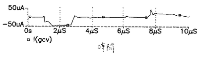
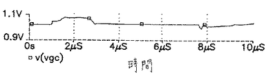
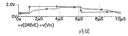
図7は、図6の回路に対応する代表的な波形を、時間の関数として図示する。図7aは、ダイオード630における電流を示す。図7bは、コンデンサ760および780における電流を示す。図7cは、トランスコンダクタンス増幅器400における電流を示す。図7dは、トランスコンダクタンス増幅器410における電流を示す。図7eは、トランスコンダクタンス増幅器420の出力での電圧を示す。図7fは、センス増幅器430の出力での電圧を示す。図7gは、電圧VdriveおよびVinを示す。図7hは、出力電流および出力電圧を示す。
【0085】
当業者は、デュアル出力端子を有する出力スルー制御を用いた切換モード電力供給コントローラが、プッシュ−プル用途での使用のために提供され得ることを容易に認識するであろう。そのような実施形態においては、センス増幅器およびGC増幅器は、別個のGVおよびGVC増幅器およびドライバに対して共通であり得る(すなわち、両方の出力が、単一のセンス増幅器を共有し得る)。
【0086】
完全なスイッチャが、図8に図示されている。完全なスイッチャは、ドライバブロック1020を含む。ドライバブロック1020は、調整された電圧Vregを生成する低ドロップアウト直線レギュレータ等の電圧レギュレータを含有し得る。完全なスイッチャは、デカップリングコンデンサ1000、並びにノードRVslewおよびRCslew(図9に図示されるノード)に接続された抵抗器1300および1310等の電圧および電流スルーを調節するための追加回路機構も備え得る。スイッチングレギュレータコントローラにおけるスルー制御のさらなる単純化は、エラー増幅器の出力端子およびフィードバックピンFBからの情報を用いて得られ得る。スタートアップ間に、より高い効率(より速いスルー)を有することが望ましい。システムが調整を開始すると、スルーは、オシレータ/論理ブロック1200の作用によって増加し、それによってシステムを静止させる。
【0087】
図9は、図8の完全なスイッチャ回路のトランスコンダクタンス増幅器1040、トランスコンダクタンス増幅器1050、出力バッファ増幅器1045(バイアス回路を含む)、トランスコンダクタンス増幅器1060、およびセンス増幅器1080の、可能なトランジスタレベルの実施形態を図示し、電流スルーフィードバックから電圧スルーフィードバックへの切り換えを促進し、重畳するフィードバックループおよび装置の制限を補償するための切換回路1400を含む。
【0088】
スルー制御回路の別の実施形態が、図10に図示される。図10は、図6の回路に対応する単一の制御抵抗器スルー制御回路である。この実施形態においては、電圧スルー制御は、図6を参照して上に説明したようなもの、すなわち、コンデンサ1590によるフィードバックを介する。電流の検出および増幅は、トランジスタ1570および関連の抵抗器によって行われる。電流スルーフィードバックは、共通駆動ノード1640に直接供給するコンデンサ1560によって行われる。この実施形態においては、電圧および電流スルーレートは、単一の素子(コンデンサ1590)によって調節され、従って、提携している。
【0089】
インダクタ電流の高周波成分の向上した制御レベルを提供するためには、電流の高次導関数が、有限で、満足に作用するべきである。インダクタの電圧スルー(dv/dt)は、
【0090】
【数6】
で表され得るので、インダクタの電圧スルーは、電流の第二次導関数を制御することによって制御され得ることになる。従って、インダクタ電流高調波は、図11に図示されるような電流スルー制御フィードバックループ1797に接続された第二次導関数ループ1795を用いて、インダクタ電流の第二次導関数を制御して電流の遷移の角を和らげることによって、さらに減衰され得る。実際には、第二次導関数ループ1795は、電流スルー制御フィードバックループ1797からの電流スルー制御フィードバック信号を変化させる。これにより、より高い周波数でより有用な、追加の20dBのロールオフが加えられる。第二次導関数(d2i/dt2)は、第一次導関数(di/dt)の変化率を表し、従って、遷移がどの位急激(sharp)であるかの良い指標である。電圧スルーフィードバックループは、必要ではない。付加的利点としては、インダクタの電圧スルーを制御することにより、追加のノイズ成分を生成し得る寄生容量(CQparasiticおよびCLparasitic)電流が減少する。従って、誘電負荷に関しては、電流スルー(di/dt)を制御するのみではなく、電流の第二次導関数も制御することが望ましい。電圧スルー(dv/dt)を制御することにより、電流の第二次導関数が制御され、高周波ノイズへの寄生成分の付加の減少も助けられる。
【0092】
高周波信号高調波のより大幅な減少は、図12に図示されるように、信号の高次導関数(例えば、出力電圧の第M次導関数および出力電流の第N次導関数)を制御することにより得られ得る。電圧および電流スルー信号の一般的な式は、それぞれ、
【0093】
【数7】
および
【0095】
【数8】
である。これらの波形に関しては、第一次導関数が、有限であり、制御されるだけでなく、高次導関数も有限であり、制御され、その結果、波形の突然の遷移が排除される。これを行う1つの方法は、デュアルフィードバックループ方法において、異なるフィードバックフィルタを作成することによる。別の方法は、開ループシステムにおいてtanh(双曲線タンジェント)形状の波形を生成することである。
【0097】
上記の本発明の実施形態は、高調波を制御するためのフィードバックとして出力電圧および出力電流導関数を使用する。しかし、本発明は、フィードバックを使用することに限定されない。図13に図示されるように、駆動信号が増幅され、負荷に直接印加される開ループ方法において出力電圧および出力電流の第一次および高次導関数を使用することが可能である。
【0098】
従って、スイッチング誘導負荷から高周波ノイズを減少させるために波形の成形を用いる装置および方法が理解される。当業者は、限定する目的ではなく、例示目的で示された記載の実施形態以外によって本発明が実施され得、本発明は、特許請求の範囲によってのみ限定されることを理解するであろう。
【0099】
【発明の効果】
本発明の低ノイズスイッチングレギュレータによれば、回路性能を犠牲にすることなく、あるいは、別の構成要素を加えることなく、誘導性負荷を切り換えることによって生じる高周波数雑音成分を低減する装置およびその方法を提供することができる。
【0100】
また、本発明の低ノイズスイッチングレギュレータによれば、高周波含有量と変換効率との間のトレードオフについてさらなる制御を可能にすることができる。
【図面の簡単な説明】
【図1】AおよびBは、信号波形エッジの鋭さの関数としての信号波形の周波数含有量を示す図である(Mark Naveによる「切換られたモードの電源おける伝導放出の予測(Prediction of Conducted Emissions in Switched Mode Power Supplies)」、1986年の電磁波適合性に関するIEEE国際シンポジウム(1986 IEEE International Symposium on Electromagnetic Compatibility 173頁)。
【図2】先行技術のブーストスイッチングレギュレータ回路を示す図である。
【図3】電流および電圧のスルー制御を示す図である。
【図4】AおよびBは、図3のフロー図に対応する代表的な波形図である。
【図5】スルー制御回路の実施形態を示す図である。
【図6】図5のスルー制御回路のトランジスタレベルの実施形態を示す図である。
【図7】A〜Hは、図6の回路に対応する代表的な波形図である。
【図8】出力スルー制御を用いた完全なスイッチャのブロック図である。
【図9】図8の出力ドライバブロックのトランジスタレベルの実施形態を示す図である。
【図10】出力スルー制御を用いた、切換られたモードの電源コントローラの1つの制御抵抗器の実施形態を示す図である。
【図11】電圧スルーを電流の第二次導関数によって制御するスルー制御回路の実施形態を示す図である。
【図12】より高次のスルー制御を用いる回路の実施形態を示す図である。
【図13】開ループスルー制御回路を示す図である。
【符号の説明】
205 駆動ノード
210 加算器
220 駆動増幅器
230 誘導性負荷
240 抵抗器240
250 センスアンプ
260 微分増幅器
270 制限器
290 微分増幅器
300 信号ノード
310 出力ノード[0001]
BACKGROUND OF THE INVENTION
The present invention relates to an apparatus and method for reducing high frequency noise caused by switching (also referred to as “driving”) an inductive load using waveform shaping. Specifically, the present invention relates to an apparatus and method for reducing high frequency noise caused by switching inductive loads using current slew control and voltage slew control. Here, “through” refers to the slope (or rate of change) of the waveform.
[0002]
[Prior art]
An increasingly important issue in the design of electrical products is high frequency electromagnetic noise. This noise can reduce product performance or cause interference with other products. Attempts to eliminate this noise source and reduce the effects of noise have expended enormous energy and cost. In electrical devices such as motors, solenoids, and switching regulators, switching currents and switching voltages are ubiquitous noise sources. Newer products such as mobile phones require even lower levels of conducted and radiated electromagnetic noise to operate properly. Laws concerning the suppression of electromagnetic pollution are also increasing. The European emission / magnetic susceptibility standard is a good example.
[0003]
[Problems to be solved by the invention]
A sharp transition of the waveform includes more high frequency components. This can be shown mathematically by Fourier series and Fourier transform. For example, a pure sine wave has one frequency component, a square wave has more high frequency components, and its amplitude decreases with frequency. A reduction in the content of high frequency means a reduction in the sharpness of the transition.
[0004]
1A and 1B show a simple thumb law for high frequency components. For a square wave, the magnitude of the high frequency component decreases from the fundamental frequency shown below at a rate of 20 dB / DECADE.
[0005]
[Expression 1]
Here, “on-time” is the time during which the switch conducts current.
[0007]
A waveform having a through edge is a waveform having a transition with a substantially constant slope, that is, a ramp signal. This means that the first derivative of the waveform is controlled. Corrugations with through edges often have rounded corners. In a waveform with a through edge and a constant first derivative, the high frequency component rolls off at 20 dB / DECADE from the fundamental frequency and rolls off at 40 dB / DECADE from a frequency equal to:
[0008]
[Expression 2]
Where t slew Is the transition time of the through edge.
[0010]
Radiation from an electrical device can usually be considered in terms of the dominant electromagnetic field, either electric or magnetic. Either electric or magnetic fields can cause noise in the circuit. Field emission is caused by a change in voltage. Magnetic field radiation is caused by changes in current. When doing so, the radiation source is often reduced and the circuitry that receives it is shielded.
[0011]
Reduction of noise caused by the electric field can be achieved by slowing the voltage transition with an element such as a capacitor. By reducing the coupling capacity, the noise intensity at the receiving end can be reduced. This reduction in coupling capacitance is accomplished by metal enclosures and metal shields for components, wiring, and printed circuit board traces.
[0012]
It is even more difficult if it contains noise caused by a magnetic field. When reducing the intensity of the noise source, it is necessary to slow down the current transition. This slowing is often done by adding inductive elements that are usually more expensive than capacitive elements. In order to shield the element which receives it from the noise generated by the magnetic field, a special shield is required, and an expensive mu metal shield is often used as this shield. It is often difficult to provide a complete shield because noise caused by the magnetic field can generate current in nearby printed circuit board traces.
[0013]
Some switching regulator topologies incorporate high frequency filter elements into power components that can help reduce costs. However, even such topologies still often add specific components to reduce emissions.
[0014]
Adding external components inevitably increases system costs. It is therefore desirable to minimize the number of external components added. Such external components are typically added to reduce the rate of change of current and / or voltage. This can be done by diverting the high frequency components after the high frequency components have been formed (adding a filter) or by minimizing the formation of the high frequency components. However, there is a power loss due to filtering. This power loss often occurs because of a large current.
[0015]
Control of the inductor voltage slew (dv / dt) may be accomplished by forming a filter. Adding capacitance to the switching node slows down the voltage transition and absorbs high frequency components. However, due to the high currents required, capacitors can be physically large and can dissipate a significant amount of power. Thereby, switching efficiency falls.
[0016]
Switching regulators are highly desirable due to their conversion efficiency. However, this conversion efficiency is obtained at the expense of creating current and voltage waveforms that contain more high frequency electromagnetic waves. This high frequency noise is coupled to nearby circuitry by conduction or radiated electromagnetic coupling (capacitive and inductive). Switching regulator designers are often forced to compromise between efficiency, noise and performance.
[0017]
In a switching regulator, most of the electromagnetic interference occurs due to the following four factors. (1) The inductor current changes abruptly, which creates high frequency magnetic noise and causes changes in nearby lines; (2) The inductor current changes, which causes the equivalent series resistance of the decoupling capacitor ( The voltage suddenly changes due to "ESR") and equivalent series inductance ("ESL"); (3) the voltage suddenly changes in the output switching element capacitively coupled to ground, thereby causing a transient in the power line; (4) When the diode is turned off, an abrupt current transient occurs, a high frequency magnetic noise is generated, and a high frequency voltage transient can be generated via the capacitor ESR.
[0018]
Interfering noise is also introduced into other circuits by conduction in power and ground wiring and capacitive or electromagnetic radiation coupling from “high temperature” components to other circuits. Typically, conducted noise is more problematic for low frequencies and radiated noise is more problematic for high frequencies. In the case of a switching regulator, the current of the inductor or transformer and the current of the switching element are usually the most troublesome noise sources because they are the largest currents. Similarly, the voltage excursion in a switch of a switching regulator is often the largest noise source due to its transition speed and connection to the power path.
[0019]
In view of the above, an apparatus and method for reducing high-frequency noise components generated by switching inductive loads without sacrificing circuit performance or adding another component Would be desirable.
[0020]
It would also be desirable to allow further control over the trade-off between harmonic content and conversion efficiency.
[0021]
[Means for Solving the Problems]
The low noise switching regulator according to the present invention is a low noise switching regulator for driving an inductive load and includes a control circuit mechanism that is responsive to current and voltage slew signals, thereby achieving the above object.
[0022]
The switching regulator may include a driver connected to the load, a current slew control feedback loop connected to the driver, and a voltage slew control feedback loop connected to the load.
[0023]
For one or more positive integers M and N, the voltage slew control feedback loop generates a first feedback signal that is proportional to the sum of one or more derivatives of the load from the first order to the Mth order. And the current slew control feedback loop may generate a second feedback signal that is proportional to the sum of one or more derivatives of the first through Nth orders of current through the load.
[0024]
The drive voltage, the output of the current slew control feedback loop, and the output of the voltage slew control feedback loop may be summed to form an input to the driver.
[0025]
The load is connected between a signal node and an output node, an input of the current slew control feedback loop is connected to the signal node, and an input of the voltage slew control feedback loop is connected to the output node. May be.
[0026]
The driver may include a drive amplifier.
[0027]
The voltage slew control feedback loop may include a differential amplifier.
[0028]
The current slew control feedback loop may include a sense amplifier connected to the signal node via a resistor and a differential amplifier connected to the sense amplifier.
[0029]
The absolute value of the amplitude of the drive voltage is limited to a first value, the absolute value of the output of the differential amplifier is limited to a second value, and the output of the differential amplifier is multiplied by a third value. And the third value may be equal to the first value divided by the second value.
[0030]
Voltage slew control may be achieved by controlling the second derivative of the current through the load.
[0031]
A second derivative, wherein the switching regulator is connected to the driver connected to the load; a current slew control feedback loop connected to the load; and an output of the current slew control feedback loop and combined with the output. And a loop.
[0032]
The switching regulator may include an open loop control system.
[0033]
A low noise switching regulator according to the present invention is a low noise switching regulator for driving an inductive load of a low noise switching regulator, the driver comprising a switch having a switch input terminal connected to the load and a switch output terminal, A current slew control feedback loop connected to the switch output terminal and a voltage slew control loop connected to the switch output terminal, thereby achieving the above object.
[0034]
The switch further includes a switch control terminal, the driver further includes a buffer amplifier connected in series between the drive node and the switch control terminal, and the current slew control feedback loop includes: the switch output terminal; A resistor connected between ground; a sense amplifier having a first input connected to the switch output terminal and a second input connected to ground; an output of the sense amplifier; and a current A first capacitor connected between the slew control feedback node; a negative input connected to the current slew control feedback node; a positive input connected to a reference potential power supply; and the current slew control feedback A first transconductance amplifier having an output connected to the node; and the current slew control feedback node And a second transconductance amplifier having a first input connected, a second input connected to the power supply at a reference potential, and an output connected to the drive node. The loop may comprise a second capacitor connected between the load and the drive node.
[0035]
And a third transconductance amplifier having a first input connected to the power supply of the drive voltage, a second input connected to the power supply of a reference potential, and an output connected to the drive node. Also good.
[0036]
A low noise switching regulator according to the present invention is a low noise switching regulator for driving an inductive load connected between a signal node and an output node, the driving node, a first adder input, a second adder, An adder having an adder input, a third adder input, an adder output, a first limiter connected between the drive node and the first adder input, A first differential amplifier having an output connected to a third adder input; an input connected to the output node; and an output connected to the second adder input; A sense amplifier connected to the signal node through a resistor, and a second differential amplifier including an output, the second differential amplifier connected to the output of the sense amplifier; The second system including the output A second limiter connected to the output of the second differential amplifier, and the output of the second limiter connected to the input of the multiplier. A drive amplifier having two limiters, an input connected to the adder output, and an output connected to the signal node, thereby achieving the above objective.
[0037]
The first limiter limits the absolute value of the amplitude of the drive voltage to a first value, and the second limiter limits the absolute value of the output of the differential amplifier to a second value; The multiplier may multiply the output of the differential amplifier by a third value.
[0038]
The third value may be equal to the first value divided by the second value.
[0039]
A method of controlling a switching regulator according to the present invention is a method of controlling a switching regulator that uses a drive voltage to drive an inductive load, the load being connected between a signal node and an output node, and one or more Generating a first feedback signal proportional to the Mth derivative of the load voltage with respect to positive integers M and N, and a second proportional to the Nth derivative of the current through the load Generating a feedback signal and combining the first and second feedback signals with the drive voltage to drive the load, thereby achieving the above objective.
[0040]
A method of controlling a switching regulator according to the present invention is a method of controlling a switching regulator that uses a drive voltage to drive an inductive load, the load being connected between a signal node and an output node, Changing the current of the node, thereby generating a first feedback signal, changing the first feedback signal, thereby generating a second feedback signal, and the first and second Combining the feedback signal with the drive voltage, thereby driving the load, thereby achieving the above objective.
[0041]
It is an object of the present invention to provide an apparatus and method for reducing high frequency noise components caused by switching inductive loads without sacrificing circuit performance or adding additional components. is there.
[0042]
Another object of the present invention is to allow further control over the trade-off between high frequency content and conversion efficiency.
[0043]
The above and other objects are achieved by switching an inductive load coupled between a signal node and an output node using a drive voltage source. This switching is done by slewing the voltage at the output node and changing the current at the signal node.
[0044]
The above and other objects and advantages of the present invention will become apparent upon consideration of the following detailed description with reference to the accompanying drawings. In the figure, the same reference numerals are assigned to the same elements.
[0045]
DETAILED DESCRIPTION OF THE INVENTION
The present invention is better understood upon consideration of the following detailed description of the preferred embodiments with reference to the accompanying drawings.
[0046]
The present invention is an apparatus and method for reducing noise caused by high frequency electrical and magnetic noise resulting from switching inductive loads.
[0047]
The present invention modifies the switching regulator controller to economically reduce electrical and magnetic frequency harmonics while at the same time allowing further control over the trade-off between harmonic content and conversion efficiency. Make it possible. Since most of the circuitry required by the present invention can be incorporated into the integrated controller, the overall system cost can also be reduced.
[0048]
Harmonics are reduced by controlling the voltage and current slew rates of the switching regulator, thereby reducing the need for filter components that handle large amounts of power. Such slew rate control is performed by reducing sudden changes in the voltage and current of the power component. In one embodiment, the output switching element has a voltage and current that is varied by a feedback control loop incorporated into the controller.
[0049]
FIG. 2 shows the drive voltage V applied to the
[0050]
Input common mode noise is the supply line (V in ) And the return line (signal ground) are defined as voltages or currents that occur in phase. That is, both the supply and return lines move in the same way with respect to ground. Input non-uniform mode noise is caused by a difference in voltage value between the supply line and the return line. Input common mode noise is likely to occur due to the voltage operating range and parasitic capacitance of the switch. Input non-uniform mode noise is likely to be caused by inductor currents that affect the impedance of the input capacitor (ie, a capacitor placed on the input voltage line to filter noise originating from the power supply). Controlling dv / dt helps reduce input common mode noise. Controlling di / dt helps reduce input non-uniform mode noise.
[0051]
A switching regulator circuit such as that shown in FIG. 2 reduces input common mode noise by changing the output of the switch (ie, providing the output with a substantially linearly increasing output voltage). As shown in FIG. miller A
[0052]
If the
[0053]
Another way that noise can occur at the output is by capacitive coupling from the switching node. Again, changing this node reduces this type of noise. One way to control voltage slew (dv / dt) (other than mirror capacitors) is by increasing the input to the drive. An example of voltage slew control is shown in Linear Technology Application Note 29.
[0054]
In the following description, a switching regulator is used as an example, but the present invention is not limited to a switching regulator. However, a switching regulator is one device in which the present invention can be implemented. The present invention is also applicable in other inductive load switching situations. Examples include motors (eg, disk drive motors), impact printer printing pins, relays, solenoids (mechanical actuators, automotive fuel injector solenoids, etc.), and phased array radar waveguide regulators.
[0055]
The conduction output noise of a switching regulator circuit depends on many factors. While circuit topology has a significant impact on noise, the dominant effect is often the switching of current to the output capacitor. This current acting through the capacitor's ESR can form a sharp voltage step. Therefore, reducing the sharpness of the current transition alleviates this problem.
[0056]
A common solution to the output noise problem is to add another filtering element. Even in this case, the need for such filtering elements can be eliminated or reduced by reducing the source of this output noise.
[0057]
Switching inductors can cause noise in the system in several ways. The first method is by magnetic radiation of the component itself. This magnetic radiation depends on the current in the device. Current can also cause noise problems acting on decoupling components. For example, the voltage generated in the ESR of the decoupling capacitor due to the inductor current. Another method is by large voltage changes. An example of a large voltage change would be a voltage “flyback” that occurs when the inductor current suddenly changes. Therefore, it is desirable to reduce the high frequency content of the inductor current. As mentioned above, the high frequency content is controlled by current slew. In the case of an inductor, the current slew (di / dt) is proportional to the voltage of the inductor, as shown in the following equation.
[0058]
[Equation 3]
The voltage value applied to the inductor is often obtained as a result of the circuit topology. The voltage can be controlled by the supply voltage, the operation of the transformer, and a clamp (such as a Zener or snubber). Thus, by limiting the voltage, the topology can primarily control the slew and therefore the primary high frequency component of the inductor current.
[0060]
In the switching regulator, the conversion efficiency is increased by reducing the power loss in the switching element. The inductor current does not change instantaneously, but the voltage can change almost instantaneously. When switching an inductor, it is usually switched between a clamp voltage and an on-state voltage. Thereby, a substantially square wave voltage is applied to the inductor.
[0061]
A switching regulator can operate in one of two modes: continuous inductor current or intermittent inductor current. In continuous mode, the current waveform is approximately triangular and current slew is controlled by voltage. In the intermittent mode, the current waveform is almost trapezoidal. The drive voltage is defined as the voltage of the inductor when the inductor is on. In either case, voltage slew is controlled by the drive voltage.
[0062]
The main concern for switching
[0063]
The present invention controls the switch dv / dt using a similar Miller capacitor that reduces input common mode noise. By incorporating capacitive feedback into the output stage design, the amount of feedback can be easily adjusted by the user and less likely to oscillate. The present invention also combines voltage slew (dv / dt) and current slew (di / dt) by summing the voltage feedback and current feedback at
[0064]
The embodiments of the present invention shown in FIGS. 3, 5, 6 and 8 attempt to control the slew rate (voltage or current) so that the derivative of the changing output (voltage or current) is constant. (Ie, making the slew constant makes the output rise linearly).
[0065]
By controlling the current slew (di / dt) of the switching element, it is a transient (and hence high frequency content) caused by a sudden change in current in the switching element, coupled to the switching element via a power connection The possible transient phenomenon can be reduced.
[0066]
The current of the switching element (for example, the above-mentioned Q switch ), The current of the diode 60 is also controlled. This is simply due to Kirchhoff's law unless the other parasitic elements are too large. This means that the current slew (di / dt) of the switching element can be controlled, and the diode current slew (di / dt) can be automatically dealt with.
[0067]
In another embodiment, the high frequency signal component can be further reduced by controlling higher order derivatives of the high frequency signal. In these waveforms, not only is the first derivative finite and controlled, but the higher order derivatives are also finite and controlled, thereby eliminating sudden transitions in the waveform. One method for performing such control is, for example, by forming a differential feedback filter by a double feedback loop method as shown in FIG. Another method is to generate a waveform such as a tanh (hyperbolic tangent) shaped waveform in an open loop system, as shown in FIG.
[0068]
As described above with reference to FIG. 2, the control of the high frequency harmonics requires the control of the output voltage slew (dv / dt) and the output current slew (di / dt) of the switching element. As shown in FIG. 4, when the output voltage and output current are controlled during the on-state, the switching element current I switch (The collector current of the switching element 40) is initially the inductor current I L1 Until the inductor current I L1 Is approximately equal to the output voltage V out Decreases. When the diode 60 becomes conductive, the output voltage V out Traces the collector voltage of the switching
[0069]
The present invention allows the output voltage and switching element current transitions to be independently controlled. This is done by providing two linked feedback paths. One of these two feedback paths is for current and the other is for voltage.
[0070]
The following description is based on a closed loop control system as shown in FIG. Needless to say, the present invention can also be applied to an open loop control system. In this case, as shown in FIG. 13, an accurately shaped waveform is amplified and an output is driven using this waveform. In order to provide a given output current and output voltage in an open loop system, knowledge of the load (eg, the impedance characteristics of the load) is required to design the drive for the output stage.
[0071]
As shown in FIG. 3, the
[0072]
FIG. 5 is a block diagram of a preferred embodiment with two feedback loops. Drive voltage V drive Is applied to the positive input terminal of
[0073]
The first feedback loop of FIG. 5, the voltage slew control loop, includes a
[0074]
The second feedback loop of FIG. 5, the current slew control loop, includes a
[0075]
[Expression 4]
Where A represents an additional gain variable. This loop controls the current slew (di / dt) of the
[0077]
Since the two loops share a common drive node, both loops affect each other, allowing a smooth transition between voltage and current changes.
[0078]
Current i Cslew , Capacitor C C The sense amplifier and the sense resistor together control the current slew rate. Current i Vslew And capacitor C V Controls the voltage slew rate. The approximate formula is:
[0079]
[Equation 5]
It is.
[0081]
One limitation of the circuit of FIG. 5 is abrupt clamping off of the output voltage by the
[0082]
During output turn-off,
[0083]
FIG. 6 illustrates a
[0084]
FIG. 7 illustrates a representative waveform corresponding to the circuit of FIG. 6 as a function of time. FIG. 7 a shows the current in the diode 630. FIG. 7 b shows the current in
[0085]
One skilled in the art will readily recognize that a switched mode power supply controller with output slew control having dual output terminals can be provided for use in push-pull applications. In such an embodiment, the sense amplifier and G C The amplifier is a separate G V And G VC It can be common for amplifiers and drivers (ie, both outputs can share a single sense amplifier).
[0086]
A complete switcher is illustrated in FIG. The complete switcher includes a
[0087]
FIG. 9 illustrates possible transistor level implementations of the
[0088]
Another embodiment of the slew control circuit is illustrated in FIG. FIG. 10 is a single controlled resistor slew control circuit corresponding to the circuit of FIG. In this embodiment, the voltage slew control is as described above with reference to FIG. 6, ie via feedback by
[0089]
In order to provide an improved control level of the high frequency component of the inductor current, the higher order derivatives of the current should be finite and work satisfactorily. The voltage slew (dv / dt) of the inductor is
[0090]
[Formula 6]
So that the voltage slew of the inductor can be controlled by controlling the second derivative of the current. Thus, the inductor current harmonic is controlled by controlling the second derivative of the inductor current using a second
[0092]
A more significant reduction in high frequency signal harmonics controls the higher order derivatives of the signal (eg, the Mth derivative of the output voltage and the Nth derivative of the output current), as illustrated in FIG. Can be obtained. The general equations for voltage and current slew signals are respectively
[0093]
[Expression 7]
and
[0095]
[Equation 8]
It is. For these waveforms, not only is the first derivative finite and controlled, but the high order derivative is also finite and controlled, thus eliminating sudden transitions in the waveform. One way to do this is by creating different feedback filters in the dual feedback loop method. Another method is to generate a tanh (hyperbolic tangent) shaped waveform in an open loop system.
[0097]
The above-described embodiments of the present invention use the output voltage and output current derivatives as feedback to control harmonics. However, the present invention is not limited to using feedback. As illustrated in FIG. 13, it is possible to use the first and higher order derivatives of the output voltage and output current in an open loop method where the drive signal is amplified and applied directly to the load.
[0098]
Accordingly, an apparatus and method that uses waveform shaping to reduce high frequency noise from switching inductive loads is understood. Those skilled in the art will appreciate that the invention can be practiced other than the described embodiments shown for purposes of illustration and not limitation, and that the invention is limited only by the claims.
[0099]
【The invention's effect】
In accordance with the low noise switching regulator of the present invention, an apparatus and method for reducing high frequency noise components generated by switching inductive loads without sacrificing circuit performance or adding additional components. Can be provided.
[0100]
Moreover, according to the low noise switching regulator of the present invention, it is possible to further control the trade-off between the high frequency content and the conversion efficiency.
[Brief description of the drawings]
FIGS. 1A and 1B are diagrams showing the frequency content of a signal waveform as a function of signal waveform edge sharpness (“Prediction of Conducted Emissions by Mark Nave” in Switched Mode Power Supplies), 1986 IEEE International Symposium on Electromagnetic Compatibility (page 173).
FIG. 2 illustrates a prior art boost switching regulator circuit.
FIG. 3 is a diagram illustrating through control of current and voltage.
4A and 4B are representative waveform diagrams corresponding to the flow diagram of FIG.
FIG. 5 is a diagram illustrating an embodiment of a through control circuit.
6 illustrates a transistor level embodiment of the slew control circuit of FIG.
7A to 7H are typical waveform diagrams corresponding to the circuit of FIG.
FIG. 8 is a block diagram of a complete switcher using output slew control.
9 is a diagram illustrating a transistor level embodiment of the output driver block of FIG. 8. FIG.
FIG. 10 illustrates an embodiment of one control resistor of a switched mode power supply controller using output slew control.
FIG. 11 illustrates an embodiment of a slew control circuit that controls voltage slew by a second derivative of current.
FIG. 12 illustrates an embodiment of a circuit that uses higher order slew control.
FIG. 13 shows an open loop through control circuit.
[Explanation of symbols]
205 Driving node
210 Adder
220 Drive amplifier
230 Inductive load
240
250 sense amplifier
260 Differential Amplifier
270 Limiter
290 Differential amplifier
300 Signal node
310 Output node
Claims (19)
前記制御回路は、
前記負荷に接続されたドライバと、
前記ドライバに接続された電流スルー制御フィードバックループであって、負荷電流が変化するレートに基づいて、前記ドライバにフィードバックを提供する電流スルー制御フィードバックループと、
前記負荷に接続された電圧スルー制御フィードバックループであって、前記負荷にかかる電圧が変化するレートに基づいて、前記ドライバにフィードバックを提供する電圧スルー制御フィードバックループと
を含む、低ノイズスイッチングレギュレータ。A low-noise switching regulator for driving an inductive load, seen including a control circuit responsive to the current through signal and voltage slew signals,
The control circuit includes:
A driver connected to the load;
A current slew control feedback loop connected to the driver, wherein the current slew control feedback loop provides feedback to the driver based on the rate at which load current changes;
A voltage slew control feedback loop connected to the load, wherein the voltage slew control feedback loop provides feedback to the driver based on a rate at which the voltage across the load changes;
Including low noise switching regulator.
前記電圧スルー制御フィードバックループが、前記負荷にかかる電圧の第1次から第M次の1つ以上の導関数の合計に比例する第1のフィードバック信号を生成し、
前記電流スルー制御フィードバックループが、前記負荷を通る電流の第1次から第N次の1つ以上の導関数の合計に比例する第2のフィードバック信号を生成する、請求項1に記載の低ノイズスイッチングレギュレータ。For positive integers M and N greater than or equal to 1,
It said voltage slew control feedback loop generates a first feedback signal proportional to the sum of the M-th order one or more derivatives from the primary voltage according to the load,
Said current slew control feedback loop generates a second feedback signal proportional to the sum of one or more derivatives from the first order of the N-th current through the load, low noise according to claim 1 Switching regulator.
前記電流スルー制御フィードバックループの入力が、前記信号ノードに接続されており、
前記電圧スルー制御フィードバックループの入力が、前記出力ノードに接続されている、請求項3に記載の低ノイズスイッチングレギュレータ。The load is connected between a signal node and an output node,
Input of the current slew control feedback loop is connected to said signal node,
The input of the voltage slew control feedback loop, Ru Tei connected to said output node, low-noise switching regulator of claim 3.
抵抗器を介して前記信号ノードに接続されたセンス増幅器と、
前記センス増幅器に接続された微分増幅器と
を含む、請求項4に記載の低ノイズスイッチングレギュレータ。The current slew control feedback loop is
A sense amplifier connected to the signal node via a resistor;
And a differential amplifier connected to said sense amplifiers, low-noise switching regulator of claim 4.
前記微分増幅器の出力の絶対値が、第2の値に制限され、
前記微分増幅器の出力が、第3の値によって乗算され、前記第3の値は、前記第2の値によって除算された前記第1の値に等しい、請求項7に記載の低ノイズスイッチングレギュレータ。The absolute value of the amplitude of the drive voltage is limited to a first value;
The absolute value of the output of the differential amplifier is limited to a second value;
The output of the differential amplifier is multiplied by a third value, said third value is equal to said first value divided by the second value, low-noise switching regulator of claim 7.
前記電流スルー制御フィードバックループの出力に接続され、前記電流スルー制御フィードバックループの出力と組み合わせられる第二次導関数ループをさらに含む、請求項1に記載の低ノイズスイッチングレギュレータ。The control circuit includes:
The current is connected to the output of the slew control feedback loop further includes a second derivative loop that in combination with the output of said current slew control feedback loop, low-noise switching regulator of claim 1.
スイッチを備えたドライバであって、前記スイッチは、スイッチ入力端子とスイッチ出力端子とを有し、前記スイッチ入力端子が前記負荷に接続されている、ドライバと、
前記スイッチ出力端子に接続された電流スルー制御フィードバックループと、
前記スイッチ出力端子に接続された電圧スルー制御ループと
を含む低ノイズスイッチングレギュレータ。A low noise switching regulator for driving an inductive load,
A driver with a switch, said switch, possess a switch input terminal and the switch output terminal, said switch input terminal is connected to the load, and a driver,
A current slew control feedback loop coupled to said switch output terminal,
Low-noise switching regulator and a voltage slew control loop coupled to said switch output terminal.
前記ドライバが、駆動ノードと前記スイッチ制御端子との間に直列で接続されたバッファ増幅器をさらに含み、
前記電流スルー制御フィードバックループが、
前記スイッチ出力端子と接地との間に接続された抵抗器と、
前記スイッチ出力端子に接続された第1の入力と、接地に接続された第2の入力とを有するセンス増幅器と、
前記センス増幅器の出力と、電流スルー制御フィードバックノードとの間に接続された第1のコンデンサと、
前記電流スルー制御フィードバックノードに接続された負の入力と、参照電位の電源に接続された正の入力と、前記電流スルー制御フィードバックノードに接続された出力とを有する第1のトランスコンダクタンス増幅器と、
前記電流スルー制御フィードバックノードに接続された第1の入力と、参照電位の前記電源に接続された第2の入力と、前記駆動ノードに接続された出力とを有する第2のトランスコンダクタンス増幅器と
を備え、
前記電圧スルー制御ループが、前記負荷と前記駆動ノードとの間に接続された第2のコンデンサを備える、請求項12に記載の低ノイズスイッチングレギュレータ。The switch further includes a switch control terminal;
Said driver further comprises a buffer amplifier connected in series between a drive node and said switch control terminal,
Said current slew control feedback loop,
A resistor connected between the switch output terminal and ground ;
A first input coupled to said switch output terminal, a sense amplifier having a second input connected to ground,
A first capacitor connected between the output of the sense amplifier and a current slew control feedback node ;
And negative input coupled to said current slew control feedback node, a positive input connected to a reference potential power source, a first transconductance amplifier having an output connected to said current slew control feedback node,
A first input coupled to said current slew control feedback node, a second input connected to said power source of the reference potential, and a second transconductance amplifier having an output connected to said driving node Prepared,
Said voltage slew control loop comprises a second capacitor connected between said load and said drive node, low-noise switching regulator of claim 12.
駆動ノードと、
第1の加算器入力と、第2の加算器入力と、第3の加算器入力と、加算器出力とを有する加算器と、
前記駆動ノードと前記第1の加算器入力との間に接続された第1の制限器と、
前記第3の加算器入力に接続された出力を有する乗算器と、
前記出力ノードに接続された入力と、前記第2の加算器入力に接続された出力とを有する第1の微分増幅器と、
出力を有するセンス増幅器であって、抵抗器を通して前記信号ノードに接続されたセンス増幅器と、
出力を有する第2の微分増幅器であって、前記センス増幅器の出力に接続された第2の微分増幅器と、
出力を有する第2の制限器であって、前記第2の制限器は、前記第2の微分増幅器の出力に接続されており、前記第2の制限器の出力は、前記乗算器の入力に接続されている、第2の制限器と、
前記加算器出力に接続された入力と、前記信号ノードに接続された出力とを有する駆動増幅器と
を含む低ノイズスイッチングレギュレータ。 A low noise switching regulator for driving an inductive load connected between a signal node and an output node,
A driving node;
An adder having a first adder input, a second adder input, a third adder input, and an adder output;
A first limiter coupled between said first adder input and the drive node,
A multiplier having an output connected to said third adder input,
An input connected to said output node, a first differential amplifier having a output connected to said second adder input,
A sense amplifier having an output, and a sense amplifier connected to said signal node through a resistor,
A second differential amplifier having an output, a second differential amplifier connected to the output of the sense amplifier,
A second limiter having an output, said second limiter, said being connected to the output of the second differential amplifier, the output of the second limiter, the input of the multiplier A second limiter connected;
Low-noise switching regulator and a drive amplifier having an input connected to said adder output, and a coupled output to the signal node.
前記第2の制限器が、前記微分増幅器の出力の絶対値を第2の値に制限し、
前記乗算器が、前記微分増幅器の出力を第3の値で乗算する、請求項15に記載の低ノイズスイッチングレギュレータ。The first limiter limits the absolute value of the amplitude of the drive voltage to a first value;
The second limiter limits the absolute value of the output of the differential amplifier to a second value;
The low noise switching regulator of claim 15 , wherein the multiplier multiplies the output of the differential amplifier by a third value.
前記負荷にかかる電圧の第M次導関数に比例する第1のフィードバック信号を生成する工程と、
前記負荷を通る電流の第N次導関数に比例する第2のフィードバック信号を生成する工程と、
前記第1および第2のフィードバック信号を前記駆動電圧と組み合わせることにより、前記負荷を駆動する工程と
を含む、方法。A method for controlling a switching regulator using the driving voltage to drive an inductive load, the load is connected between a signal node and an output node, with respect to one or more positive integer M and N, The method
Generating a first feedback signal proportional to the M derivative of the voltage applied to the load,
Generating a second feedback signal proportional to the N derivative of the current through the load,
Wherein the first and second feedback signals the drive voltage and the combination Rukoto, and a step of driving the load, method.
前記方法は、
前記信号ノードの電流を変化させることにより、第1のフィードバック信号を生成する工程と、
前記第1のフィードバック信号を変化させることにより、第2のフィードバック信号を生成する工程と、
前記第1および第2のフィードバック信号を前記駆動電圧と組み合わせることにより、前記負荷を駆動する工程と
を含む、方法。A method for controlling a switching regulator using the driving voltage to drive an inductive load, the load is connected between a signal node and an output node,
The method
The Rukoto varying the current of the signal node, generating a first feedback signal,
The Rukoto changing said first feedback signal, and generating a second feedback signal,
Wherein the first and second feedback signals the drive voltage and the combination Rukoto, and a step of driving the load, method.
Applications Claiming Priority (2)
| Application Number | Priority Date | Filing Date | Title |
|---|---|---|---|
| US08/840,017 | 1997-04-24 | ||
| US08/840,017 US5952817A (en) | 1997-04-24 | 1997-04-24 | Apparatus and method using waveform shaping for reducing high frequency noise from switching inductive loads |
Publications (2)
| Publication Number | Publication Date |
|---|---|
| JPH1141918A JPH1141918A (en) | 1999-02-12 |
| JP4065601B2 true JP4065601B2 (en) | 2008-03-26 |
Family
ID=25281248
Family Applications (1)
| Application Number | Title | Priority Date | Filing Date |
|---|---|---|---|
| JP11573798A Expired - Lifetime JP4065601B2 (en) | 1997-04-24 | 1998-04-24 | Low noise switching regulator and method for controlling a switching regulator |
Country Status (5)
| Country | Link |
|---|---|
| US (1) | US5952817A (en) |
| EP (1) | EP0874461B1 (en) |
| JP (1) | JP4065601B2 (en) |
| DE (1) | DE69834978T2 (en) |
| TW (1) | TW451546B (en) |
Families Citing this family (18)
| Publication number | Priority date | Publication date | Assignee | Title |
|---|---|---|---|---|
| JP4490586B2 (en) * | 1998-10-30 | 2010-06-30 | シーメンス ヴィディーオー オートモーティヴ コーポレイション | Device for reducing electromagnetic radiation in a circuit by slewing voltage and current |
| US6040686A (en) * | 1999-01-07 | 2000-03-21 | Linear Technology Corporation | Low noise step-down switching regulator circuits with programmable slew rate limiter and methods of use |
| DE19934270B4 (en) * | 1999-07-21 | 2008-05-15 | Audi Ag | Vehicle flashing system with a circuit arrangement for suppressing interference signals |
| US6487097B2 (en) * | 2000-03-16 | 2002-11-26 | Altel Technology | Feedforward clamping applied to the control voltage in switch mode power supplies (SMPS) |
| DE10196950T5 (en) * | 2000-11-27 | 2004-07-22 | Seagate Technology Llc, Scotts Valley | Engine start-up current control device and method |
| DE10061563B4 (en) * | 2000-12-06 | 2005-12-08 | RUBITEC Gesellschaft für Innovation und Technologie der Ruhr-Universität Bochum mbH | Method and apparatus for switching on and off of power semiconductors, in particular for a variable-speed operation of an asynchronous machine, operating an ignition circuit for gasoline engines, and switching power supply |
| US6882549B2 (en) | 2001-03-21 | 2005-04-19 | Honeywell International Inc. | Active filter for power distribution system with selectable harmonic elimination |
| US7154248B2 (en) * | 2004-07-15 | 2006-12-26 | Teleflex Canada Inc. | Control system for an electric machine |
| DE102005037985B3 (en) * | 2005-08-05 | 2006-08-03 | Dmos Gmbh | Electronic switching arrangement e.g. direct current motor, switching method, involves comparing interfering signal and reference level and transmitting comparison result by programming unit that produces parameter set for control switching |
| US7199565B1 (en) * | 2006-04-18 | 2007-04-03 | Atmel Corporation | Low-dropout voltage regulator with a voltage slew rate efficient transient response boost circuit |
| US7683592B2 (en) * | 2006-09-06 | 2010-03-23 | Atmel Corporation | Low dropout voltage regulator with switching output current boost circuit |
| CN101859161A (en) * | 2010-06-17 | 2010-10-13 | 华为技术有限公司 | Low voltage source bandgap reference voltage circuit and integrated circuit |
| EP2615737B1 (en) * | 2012-01-13 | 2021-05-05 | ABB Schweiz AG | Active gate drive circuit |
| US9134743B2 (en) * | 2012-04-30 | 2015-09-15 | Infineon Technologies Austria Ag | Low-dropout voltage regulator |
| KR101989575B1 (en) | 2012-12-07 | 2019-06-14 | 삼성전자주식회사 | Adaptive power converting device |
| US9184744B2 (en) * | 2014-03-14 | 2015-11-10 | Infineon Technologies Ag | Gate signal generation with adaptive signal profiles |
| US9672582B2 (en) * | 2014-12-05 | 2017-06-06 | Toyota Motor Engineering & Manufacturing North America, Inc. | Systems and methods for Gaussian filter standard deviation variation |
| US9847724B2 (en) | 2015-10-06 | 2017-12-19 | Keithley Instruments, Llc | Power supply having reduced transformer commutation noise |
Family Cites Families (12)
| Publication number | Priority date | Publication date | Assignee | Title |
|---|---|---|---|---|
| US4540893A (en) * | 1983-05-31 | 1985-09-10 | General Electric Company | Controlled switching of non-regenerative power semiconductors |
| US4591734A (en) * | 1984-04-27 | 1986-05-27 | General Electric Company | Integratable circuit for controlling turn-off voltage rate-of-change of non-regenerative voltage-controlled switching semiconductor devices |
| US4633150A (en) * | 1984-12-25 | 1986-12-30 | Matsushita Electric Industrial Co., Ltd. | Driving circuit for brushless DC motors |
| US4823070A (en) * | 1986-11-18 | 1989-04-18 | Linear Technology Corporation | Switching voltage regulator circuit |
| US5153457A (en) * | 1990-12-12 | 1992-10-06 | Texas Instruments Incorporated | Output buffer with di/dt and dv/dt and tri-state control |
| JP2624382B2 (en) * | 1991-01-21 | 1997-06-25 | 株式会社三協精機製作所 | Drive circuit for brushless motor |
| US5191269A (en) * | 1991-10-10 | 1993-03-02 | Sgs-Thomson Microelectronics, Inc. | Brushless direct current motor with minimized current ripple and method |
| GB9302214D0 (en) * | 1993-02-04 | 1993-03-24 | Texas Instruments Ltd | Differential bus drivers |
| EP0678983B1 (en) * | 1994-04-22 | 1998-08-26 | STMicroelectronics S.r.l. | Output buffer current slew rate control integrated circuit |
| US5614797A (en) * | 1995-02-28 | 1997-03-25 | Sgs-Thomson Microelectronics, Inc. | Stator coil driver circuit for a brushless DC motor |
| US5708379A (en) * | 1995-07-21 | 1998-01-13 | Hewlett-Packard Company | Electronically programmable output impedance circuit |
| US5731692A (en) * | 1996-09-30 | 1998-03-24 | Lucent Technologies Inc. | System and method for limiting overshoot in a voltage and current control circuit |
-
1997
- 1997-04-24 US US08/840,017 patent/US5952817A/en not_active Expired - Lifetime
-
1998
- 1998-04-22 EP EP19980107299 patent/EP0874461B1/en not_active Expired - Lifetime
- 1998-04-22 TW TW87106162A patent/TW451546B/en not_active IP Right Cessation
- 1998-04-22 DE DE69834978T patent/DE69834978T2/en not_active Expired - Lifetime
- 1998-04-24 JP JP11573798A patent/JP4065601B2/en not_active Expired - Lifetime
Also Published As
| Publication number | Publication date |
|---|---|
| EP0874461A2 (en) | 1998-10-28 |
| EP0874461B1 (en) | 2006-06-21 |
| EP0874461A3 (en) | 2000-03-29 |
| DE69834978T2 (en) | 2006-11-09 |
| US5952817A (en) | 1999-09-14 |
| JPH1141918A (en) | 1999-02-12 |
| TW451546B (en) | 2001-08-21 |
| DE69834978D1 (en) | 2006-08-03 |
Similar Documents
| Publication | Publication Date | Title |
|---|---|---|
| JP4065601B2 (en) | Low noise switching regulator and method for controlling a switching regulator | |
| Sekiya et al. | FM/PWM control scheme in class DE inverter | |
| US6661210B2 (en) | Apparatus and method for DC-to-DC power conversion | |
| US6147478A (en) | Hysteretic regulator and control method having switching frequency independent from output filter | |
| US9973076B1 (en) | Switching regulator synchronous node snubber circuit | |
| US6710646B1 (en) | Cuk style inverter with hysteretic control | |
| US20020060621A1 (en) | System and method for orthogonal inductance variation | |
| WO2008021521A2 (en) | Power converter with hysteretic control | |
| WO2007015889A2 (en) | Current mode control with feed-forward for power devices | |
| US20040257056A1 (en) | Switching regulator with improved load transient efficiency and method thereof | |
| EP1234377B1 (en) | Power booster amplifier | |
| US10672757B2 (en) | Multiphase parallel direct-current (DC) to DC circuit and chip structure thereof | |
| JP2021191079A (en) | Dc power source device, current stabilization circuit used for the same, and noise suppression method for power source line | |
| CN101645663B (en) | Method for reducing EMI interference of secondary circuit | |
| CA1039354A (en) | Switching voltage regulator with low rfi noise | |
| CN108268695B (en) | Design method of amplifying circuit and amplifying circuit | |
| US10340790B1 (en) | Integrated voltage correction using active bandpass clamp | |
| KR101122940B1 (en) | Device for supplying an integrated circuit with power | |
| EP3220546A1 (en) | Electronic driver circuit for at least one power mosfet and method operating at least one power mosfet | |
| CN113517813B (en) | Fixed frequency dual-mode synchronous buck controller | |
| CN214069810U (en) | Voltage switching control circuit and voltage switching control device | |
| CN211352042U (en) | PCB circuit for protecting switching power supply | |
| US5952858A (en) | Junction capacitor compensation for wave shaping | |
| CN110932532A (en) | Ripple injection circuit for constant on-time control mode switching power supply | |
| JP2023156011A (en) | DC power supply |
Legal Events
| Date | Code | Title | Description |
|---|---|---|---|
| A621 | Written request for application examination |
Free format text: JAPANESE INTERMEDIATE CODE: A621 Effective date: 20050422 |
|
| A131 | Notification of reasons for refusal |
Free format text: JAPANESE INTERMEDIATE CODE: A131 Effective date: 20070718 |
|
| A601 | Written request for extension of time |
Free format text: JAPANESE INTERMEDIATE CODE: A601 Effective date: 20071015 |
|
| A602 | Written permission of extension of time |
Free format text: JAPANESE INTERMEDIATE CODE: A602 Effective date: 20071018 |
|
| A521 | Written amendment |
Free format text: JAPANESE INTERMEDIATE CODE: A523 Effective date: 20071119 |
|
| TRDD | Decision of grant or rejection written | ||
| A01 | Written decision to grant a patent or to grant a registration (utility model) |
Free format text: JAPANESE INTERMEDIATE CODE: A01 Effective date: 20071206 |
|
| A61 | First payment of annual fees (during grant procedure) |
Free format text: JAPANESE INTERMEDIATE CODE: A61 Effective date: 20080107 |
|
| R150 | Certificate of patent or registration of utility model |
Free format text: JAPANESE INTERMEDIATE CODE: R150 |
|
| FPAY | Renewal fee payment (event date is renewal date of database) |
Free format text: PAYMENT UNTIL: 20110111 Year of fee payment: 3 |
|
| FPAY | Renewal fee payment (event date is renewal date of database) |
Free format text: PAYMENT UNTIL: 20110111 Year of fee payment: 3 |
|
| FPAY | Renewal fee payment (event date is renewal date of database) |
Free format text: PAYMENT UNTIL: 20120111 Year of fee payment: 4 |
|
| FPAY | Renewal fee payment (event date is renewal date of database) |
Free format text: PAYMENT UNTIL: 20130111 Year of fee payment: 5 |
|
| FPAY | Renewal fee payment (event date is renewal date of database) |
Free format text: PAYMENT UNTIL: 20130111 Year of fee payment: 5 |
|
| R250 | Receipt of annual fees |
Free format text: JAPANESE INTERMEDIATE CODE: R250 |
|
| R250 | Receipt of annual fees |
Free format text: JAPANESE INTERMEDIATE CODE: R250 |
|
| R250 | Receipt of annual fees |
Free format text: JAPANESE INTERMEDIATE CODE: R250 |
|
| R250 | Receipt of annual fees |
Free format text: JAPANESE INTERMEDIATE CODE: R250 |
|
| R250 | Receipt of annual fees |
Free format text: JAPANESE INTERMEDIATE CODE: R250 |
|
| EXPY | Cancellation because of completion of term |