JP4058627B2 - Manufacturing method of resin lens for semiconductor optical element - Google Patents
Manufacturing method of resin lens for semiconductor optical element Download PDFInfo
- Publication number
- JP4058627B2 JP4058627B2 JP2003070210A JP2003070210A JP4058627B2 JP 4058627 B2 JP4058627 B2 JP 4058627B2 JP 2003070210 A JP2003070210 A JP 2003070210A JP 2003070210 A JP2003070210 A JP 2003070210A JP 4058627 B2 JP4058627 B2 JP 4058627B2
- Authority
- JP
- Japan
- Prior art keywords
- lens
- resin material
- semiconductor optical
- resin
- optical element
- Prior art date
- Legal status (The legal status is an assumption and is not a legal conclusion. Google has not performed a legal analysis and makes no representation as to the accuracy of the status listed.)
- Expired - Lifetime
Links
Images


Landscapes
- Casting Or Compression Moulding Of Plastics Or The Like (AREA)
- Led Device Packages (AREA)
Description
【0001】
【発明の属する技術分野】
本発明は、半導体光学素子用樹脂レンズの製造方法、特に、半導体光学素子を封止するための液状の封止樹脂材料上に載置し、この封止樹脂材料を硬化させることによりその硬化物である封止材上に一体化して用いる半導体光学素子用樹脂レンズの製造方法に関する。
【0002】
【従来の技術】
発光ダイオード(LED)には、砲弾タイプ、チップタイプ等の種類があり、砲弾タイプの発光ダイオードは、一般に、カソードリード、アノードリード、発光半導体チップ、リード細線などの発光体及び導電部材を透光性の樹脂で封止した構造となっている。また、チップ型の発光ダイオードの場合も、上面が開口した箱形の発光体収容部材の内底から一対のリードフレームを発光体収容部材の外部へ延出し、この発光体収容部材の内部に発光半導体チップやリード細線等を収容し、これらを接続して、収容部材内部を透光性の樹脂で封止した構造になっており、これらの発光ダイオードには、その使用目的に応じ、封止材上に発光した光の進行方向を規制するための集光レンズが設けられる場合がある。
【0003】
これらの発光ダイオードのうち、チップ型の発光ダイオードにレンズを設ける場合、発光半導体チップ等を発光体収容部材に収容し、次いでこの収容部材に液状の封止用樹脂材料を充填し、この封止用樹脂材料上にレンズを載置して封止用樹脂材料を硬化させると共に封止材とレンズとを一体化する方法がとられるが、この場合、封止材とレンズとの間に気泡が取り残されてしまうことがあり、気泡が取り残されると残留した気泡が光の乱反射や散乱の原因となって輝度が低下するため製品不良となってしまうという問題があった。
【0004】
なお、この発明に関連する先行技術文献情報としては以下のものがある。
【0005】
【特許文献1】
特開平3−119769号公報
【特許文献2】
特開平8−99368号公報
【0006】
【発明が解決しようとする課題】
本発明は、上記事情に鑑みなされたもので、チップ型の発光ダイオードに用いられるレンズのように、半導体光学素子を封止するための液状の封止樹脂材料上に載置し、この封止樹脂材料を硬化させることによりその硬化物である封止材上に一体化して用いる半導体光学素子用樹脂レンズとして、レンズを液状の封止樹脂材料上に載置して封止樹脂材料を硬化させる際に、封止材とレンズとの間に気泡が取り残されることを可及的に防止することができる半導体光学素子用樹脂レンズを生産性よく製造できる方法を提供することを目的とする。
【0007】
【課題を解決するための手段】
本発明者は、上記課題を解決するため鋭意検討を重ねた結果、まずレンズの封止材との接合面を凸面とすれば、この曲面に沿って気泡を逃がすことができ、気泡の残留を避けることが可能であることを知見した。これにはレンズの両面が凸面をなす凸レンズが使用可能であるが、このような形状の樹脂レンズを圧縮成形により成形すると、半導体光学素子用である比較的小型の樹脂レンズを成形するためには微細な加工を施した高価な金型を用いる必要がある上に、成形品にはバリが発生しやすいことが問題となった。バリは封止材との接合の障害となるため除去する必要があるが、半導体光学素子用の小型樹脂レンズでは、バリ取りは極めて煩雑な作業であって実用的ではなく、バリが発生したものは直ちに不良品となるため、このような圧縮成形で半導体光学素子用の樹脂レンズを製造することは、歩留まりが悪いものであった。
【0008】
そこで、本発明者らは、更に検討を重ねた結果、半導体光学素子用樹脂レンズを、成形型にレンズの集光面をなす凸面を形成するための凹面を有する断面円弧状凹陥部を備えるキャビティ凹部を設け、上記キャビティ凹部に液状のレンズ用樹脂材料をこのレンズ用樹脂材料が上記キャビティ凹部の上方でその表面張力により凸面をなす液滴となるように充填し、次いで上記レンズ用樹脂材料の液滴を加熱して硬化させることにより製造すれば、両面が凸面をなす樹脂レンズが得られ、上記成形型の凹面に対応する面を集光面とし、集光面と反対側の面の凸面を封止樹脂材料(封止材)との接合面としてやれば、集光レンズとしての機能を有し、かつレンズと封止樹脂材料との間の気泡を逃がして気泡の残留を避けることが可能な凸面を有するレンズが得られると共に、このレンズは成形時に圧縮していないためバリの発生がなく歩留まりが極めて良好であり、上記半導体光学素子用の樹脂レンズ、特に発光ダイオードに用いられる比較的小型の樹脂レンズを生産性よく製造することができることを見出し、本発明をなすに至った。
【0009】
即ち、本発明は、半導体光学素子を封止するための液状の封止樹脂材料上に載置し、この封止樹脂材料を硬化させることによりその硬化物である封止材と一体化して用いられる半導体光学素子用樹脂レンズの製造方法であって、成形型にレンズの集光面となる凸面を形成するための凹面を有する断面円弧状凹陥部を備えるキャビティ凹部を設け、上記キャビティ凹部に液状のレンズ用樹脂材料をこのレンズ用樹脂材料が上記キャビティ凹部の上方でその表面張力により凸面をなす液滴となるように充填し、次いで上記レンズ用樹脂材料の液滴を加熱して硬化させることを特徴とする半導体光学素子用樹脂レンズの製造方法を提供する。
【0010】
このような半導体光学素子用樹脂レンズにおいては、その一方の面が所望の曲率を有する凸面であることが必要であるが、本発明の製造方法によれば、上記成形型の凹面を所望の曲率の凹面とすることによりこの凹面の曲率に相当する所望の凸面が集光面として形成されたレンズを製造することができる。
【0011】
一方、封止材との接合面となる面は、硬化後にレンズと封止材と接合されるため、厳密な曲率の調整を必要とせず、気泡を逃がすことのできる曲率の凸面になっていればよいが、本発明の製造方法によれば、レンズ用樹脂材料の表面張力により凸面を形成して硬化させることにより、封止樹脂材料と一体化する際に、レンズと封止樹脂材料との間に残留する気泡を逃がすに十分な曲率を有する凸面を形成することができる。
【0012】
本発明の製造方法においては、特に、上記キャビティ凹部を、円板状凹陥部と、その中央下部に形成された断面円弧状凹陥部とを備える形状に形成されたものとしてやれば、振動等の外力に抗して表面張力により形成されたレンズ用樹脂材料の液滴を安定的に形成、維持することができ、硬化前に上記液滴が崩れることを防ぐことができるため好ましい。
【0013】
【発明の実施の形態及び実施例】
以下、本発明につき更に詳述する。
本発明の半導体光学素子用樹脂レンズの製造方法は、半導体光学素子を封止するための液状の封止樹脂材料上に載置し、この封止樹脂材料を硬化させることによりその硬化物である封止材と一体化して用いられる半導体光学素子用樹脂レンズの製造方法であり、成形型にレンズの集光面となる凸面を形成するための凹面を有する断面円弧状凹陥部を備えるキャビティ凹部を設け、上記キャビティ凹部に液状のレンズ用樹脂材料をこのレンズ用樹脂材料が上記キャビティ凹部の上方でその表面張力により凸面をなす液滴となるように充填し、次いで上記レンズ用樹脂材料の液滴を加熱して硬化させることにより製造するものである。
【0014】
本発明において、半導体光学素子用樹脂レンズは、成形型にレンズの集光面となる凸面を形成するための凹面を有する断面円弧状凹陥部を備えるキャビティ凹部を設け、上記キャビティ凹部に液状のレンズ用樹脂材料をこのレンズ用樹脂材料が上記キャビティ凹部の上方でその表面張力により凸面をなす液滴となるように充填し、次いで上記レンズ用樹脂材料の液滴を加熱して硬化させることにより製造する。
【0015】
成形型として具体的には、例えば、図1(A)〜(C)に示されるような成形型2が挙げられる。図1中、2は成形型で、その上面22にはキャビティ凹部21が形成されている。この場合、このキャビティ凹部21は円板状凹陥部211と、この円板状凹陥部211の中央下部に形成された断面円弧状凹陥部212とからなる形状を有し、この断面円弧状凹陥部212の壁面212aがレンズの集光面となる凸面を形成するための凹面となるもので、このキャビティ凹部21に液状のレンズ用樹脂材料が充填される。
【0016】
本発明においては、後述するように成形時にレンズ用樹脂材料を圧縮することがないため、成形型としては、金属製、樹脂製、ゴム製のいずれも適用可能であるが、加熱硬化時又は冷却時の熱伝導性を考慮すると金属製の成形型(金型)を用いることが好ましい。
【0017】
本発明の製造方法においては、特に、上記キャビティ凹部が、円板状凹陥部と、その中央下部に形成された断面円弧状凹陥部とを備える形状に形成された成形型を用いることが好ましい。より具体的には、例えば、図1(A)〜(C)に示される成形型2のような、キャビティ凹部21が、円板状凹陥部211と、この円板状凹陥部211の中央下部に形成された断面円弧状凹陥部212とからなる形状を有しているものであれば、キャビティ凹部21の円板状凹陥部211を形成する周面211aと成形型2の上面22とが直交することとなり、例えば、図2(A)に示されるような、キャビティ凹部21が断面円弧状凹陥部212のみからなり、その壁面212aと成形型の上面22とが鈍角で交わっているような成形型よりも、振動等の外力に抗して表面張力により形成されたレンズ用樹脂材料の液滴を安定的に形成、維持することができ、硬化前に上記液滴が崩れることを防ぐことができ、また、曲率の大きい凸面を形成することが可能であることから好ましい。
【0018】
なお、本発明においては、図2(A)に示されるような成形型を用いることも可能である。また、図2(B)に示されるような、キャビティ凹部21が円板状凹陥部211と、この円板状凹陥部211の下部に形成された上記円板状凹陥部211と同径の断面円弧状凹陥部212とからなる形状を有する成形型も好適に用いることができる。
【0019】
レンズ用樹脂材料の充填及び充填されたレンズ用樹脂材料の硬化は、例えば、図3に示されるように、成形型2に形成されたキャビティ凹部21(図3(A))に液状のレンズ用樹脂材料3をこのレンズ用樹脂材料3がキャビティ凹部21の上方でその表面張力により凸面311をなす液滴31となるように、定量供給装置4で充填量を調整しながら充填(図3(B),(C))し、このレンズ用樹脂材料の液滴31を遠赤外線ヒータ51、IHヒータ52又はその両方を用いて加熱してレンズ用樹脂材料の液滴31を硬化(図3(D))させる方法などが好適である。
【0020】
レンズ用樹脂材料の液滴31を硬化させた後は、送風機61で空冷、放熱板62を介して水冷又はその両方により冷却(図3(E))し、取り出し機7で成形型2から離型(図3(F))してレンズ1を得ることができる。得られたレンズ1は、図4(A)〜(D)に示されるように、キャビティ凹部21のレンズの集光面となる凸面を形成するための凹面、即ち、断面円弧状凹陥部212の壁面212aに対応する凸面11と、レンズ用樹脂材料の液滴31の表面張力により形成された凸面311に対応する凸面13とを有するものとなり、凸面11がレンズの集光面、凸面13がレンズと封止材との接合面となる。
【0021】
なお、上記図では、成形型に1つのキャビティ凹部が形成されたものを例示したが、これに限定されるものではなく、1つの成形型の上面に複数のキャビティ凹部を設け、各々のキャビティ凹部に順に又は複数の定量供給装置を用いて一度にレンズ用樹脂材料を充填してレンズを製造することも可能である。
【0022】
本発明においては、レンズ用樹脂材料として液状のものを用いる。このようなものとしては、樹脂製レンズの製造に用いられる従来公知の液状樹脂材料を用いることができるが、特にシリコーン樹脂組成物が好ましく用いられる。このような液状のシリコーン樹脂組成物を硬化させることにより、シリコーン樹脂製のレンズを得ることができるが、シリコーン樹脂組成物としては、特に、液状の付加反応硬化型のシリコーン樹脂組成物が好ましい。液状の付加反応硬化型のシリコーン樹脂組成物は、無溶媒であるため発泡することなく表面も内部も均一に硬化させることができるので好適である。
【0023】
上記付加反応硬化型のシリコーン樹脂組成物としては、熱硬化により透明なシリコーン樹脂を形成するものであれば特に制限されないが、例えば、オルガノポリシロキサンをベースポリマーとし、オルガノハイドロジェンポリシロキサン及び白金系触媒等の重金属系触媒を含むものが挙げられる。
【0024】
上記オルガノポリシロキサンとしては、下記平均単位式
RaSiO(4-a)/2
(式中、Rは非置換又は置換一価炭化水素基で、好ましくは炭素数1〜10、特に1〜8のものである。aは0.8〜2、特に1〜1.8の正数である。)
で示されるものが挙げられる。ここで、Rとしてはメチル基、エチル基、プロピル基、ブチル基等のアルキル基、ビニル基、アリル基、ブテニル基等のアルケニル基、フェニル基、トリル基等のアリール基、ベンジル基等のアラルキル基や、これらの炭素原子に結合した水素原子の一部又は全部がハロゲン原子で置換されたクロロメチル基、クロロプロピル基、3,3,3−トリフルオロプロピル基等のハロゲン置換炭化水素基、或いはシアノ基で置換された2−シアノエチル基等のシアノ基置換炭化水素基などが挙げられ、Rは同一であっても異なっていてもよいが、Rとしてフェニル基を含むもの、特に、全Rのうち5〜80モル%がフェニル基であるものが、光学レンズの耐熱性及び透明性の点から好ましい。
【0025】
また、Rとしてビニル基等のアルケニル基を含むもの、特に全Rのうちの1〜20モル%がアルケニル基であるものが好ましく、中でもアルケニル基を1分子中に2個以上有するものが好ましく用いられる。このようなオルガノポリシロキサンとしては、例えば、末端にビニル基等のアルケニル基を有するジメチルポリシロキサンやジメチルシロキサン・メチルフェニルシロキサン共重合体等の末端アルケニル基含有ジオルガノポリシロキサンが挙げられる。
【0026】
一方、オルガノハイドロジェンポリシロキサンとしては、3官能以上(即ち、1分子中にケイ素原子に結合する水素原子(Si−H基)を3個以上有するもの)が好ましく、例えば、メチルハイドロジェンポリシロキサン、メチルフェニルハイドロジェンポリシロキサン等が挙げられ、特に、常温で液状のものが好ましい。また、触媒としては、白金、白金化合物、ジブチル錫ジアセテートやジブチル錫ジラウリレート等の有機金属化合物、又はオクテン酸錫のような金属脂肪酸塩などが挙げられる。これらオルガノハイドロジェンポリシロキサンや触媒の種類や量は、架橋度や硬化速度を考慮して適宜決定すればよい。また、上記成分以外に、得られるシリコーン樹脂の強度や透明度を損なわない程度に充填剤、耐熱材、可塑剤等を添加してもよい。上記シリコーン樹脂組成物としては、信越化学工業株式会社製 KE1935(A/B)、GE東芝シリコーン株式会社製 XE14−062,XE14−907、東レ・ダウ・コーニング・シリコーン株式会社製 SH6103,DX−35−547等の市販品を用いることができる。
【0027】
本発明において、上述した方法で得られたレンズを、半導体光学素子を封止するための液状の封止樹脂材料上に載置し、この封止樹脂材料を硬化させることによりその硬化物である封止材と一体化して用いるものであるが、例えば、発光ダイオード用のレンズ、特に、チップ型の発光ダイオード用のレンズとして好適に用いられる。
【0028】
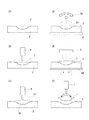
チップ型の発光ダイオードは、図5に示されるように、上面が開口した箱形の発光体収容部材105の内底から一対のリード101,102を発光体収容部材105の外部へ延出し、この発光体収容部材105の内部に発光体である発光半導体チップ103やリード細線104,104を収容し、これらを接続して、発光体収容部材105内部を封止材(透光性樹脂)106で封止した構造となっており、レンズ1はこの封止材106上に接合されて用いられる。
【0029】
このレンズ1は、発光半導体チップ103等を発光体収容部材105に収容、接続後、発光体収容部材105内に液状の封止樹脂材料106を充填してレンズ1を封止樹脂材料106上に凸面13を封止樹脂材料106側に向けて載せ、この封止樹脂材料106を加熱等によって硬化させることにより一体に接合されるが、図6(A)に示されるように、封止樹脂材料106を充填する際に封止樹脂材料106中に巻き込まれた気泡aや、レンズ1を封止樹脂材料106上に載せる際にできるレンズ1と封止樹脂材料106との間の空気層bなどを発光体収容部材105内部から完全に除かなければ、封止樹脂材料106を硬化させた後に、残留した気泡が光の乱反射や散乱の原因となって輝度が低下するため、発光ダイオードが不良品となってしまう。しかしながら、この場合、図6(B)に示されるように、封止樹脂材料106中の気泡aや封止樹脂材料106とレンズ1との間に溜まった空気層bは、浮力によって上昇し、レンズ1の凸面13に沿って図中矢印で示すようにレンズ1の外周側へと移動して、レンズ1と発光体収容部材105との間隙107から外部へと排出されるため、封止樹脂材料106を硬化させた後に、封止材とレンズとの間に気泡が取り残されてしまうことがない。
【0030】
本発明の製造方法は、径が1〜30mm程度、厚さが0.5〜30mm程度の小型の樹脂レンズを製造する場合に、特に好適である。また上記例では、半導体光学素子としてチップ型の発光ダイオードに用いる場合を例示したが、これに限定されるものではなく、例えば、受光素子チップが組み込まれた画像形成用受光素子などのレンズとして用いることも可能である。
【0031】
【実施例】
以下、実施例を挙げて本発明を具体的に説明するが、本発明は下記実施例に限定されるものではない。
【0032】
[実施例1]
レンズ用樹脂材料としてケイ素原子に結合するフェニル基を有するオルガノポリシロキサンをベースポリマーとする液状シリコーン樹脂組成物(XE14−907(GE東芝シリコーン株式会社製))を用い、これを光学的に加工した図1に示すような形状のキャビティ凹部を100個形成した金型に定量供給装置を用いて液状シリコーン組成物が表面張力により凸面をなす液滴となるように充填し、これらを加熱、硬化させ、冷却後、成形型から離型して、図4に示すような形状のシリコーン樹脂製レンズ(径6mm、厚さ3mm)を100個製造した。これらいずれのレンズにおいてもバリの発生はなく、いずれも表面張力による凸面が形成されていた。
【0033】
次に、このレンズを用いて、発光半導体チップ等を発光体収容部材に収容、接続後、発光体収容部材内に液状の封止樹脂材料を充填してレンズを封止樹脂材料上に表面張力により形成された凸面を封止樹脂材料側に向けて載せ、この封止樹脂材料を加熱等によって硬化させることにより、図5に示されるような、封止材上にレンズが一体に接合されたチップ型の発光ダイオードを製造した。このようなチップ型の発光ダイオードを100個製造したが、いずれのものもレンズと封止材との間に発光半導体チップからの光を乱反射させたり散乱させたりするような気泡の残留はなく十分な輝度を示すものであった。
【0034】
【発明の効果】
以上のように、本発明によれば、集光レンズとしての機能を有し、かつレンズと封止樹脂材料との間の気泡を逃がして気泡の残留を避けることが可能な凸面を有する半導体光学素子用の樹脂レンズを、バリの発生なく生産性よく製造することができる
【図面の簡単な説明】
【図1】本発明に係る製造方法において用いる成形型の一例を示す図であり、(A)は斜視図、(B)は平面図、(C)は(B)のX−X’線に沿った断面図である。
【図2】本発明に係る製造方法において用いる成形型の他の一例を示す断面図である。
【図3】本発明に係る製造方法によりレンズを製造する工程を説明する説明図である。
【図4】本発明に係る製造方法により製造されたレンズの一例であって、図1に示す成形型を用いて製造されたレンズを示す図であり、(A)は斜視図、(B)は平面図、(C)は(B)のY−Y’線に沿った断面図、(D)は(A)の天地を返した状態の斜視図である。
【図5】本発明に係る製造方法により製造されたレンズを用いた半導体光学素子の一例を示すものであり、チップ型の発光ダイオードを示す断面図である。
【図6】本発明に係る製造方法により製造されたレンズを用いて、チップ型の発光ダイオードを製造する過程を示す説明図である。
【符号の説明】
1 レンズ
11,13 凸面
2 成形型
21 キャビティ凹部
211 円板状凹陥部
212 断面円弧状凹陥部
3 レンズ用樹脂材料
31 液滴
311 凸面[0001]
BACKGROUND OF THE INVENTION
The present invention relates to a method for producing a resin lens for a semiconductor optical element, in particular, a liquid cured resin material for sealing a semiconductor optical element, and the cured product obtained by curing the sealing resin material. It is related with the manufacturing method of the resin lens for semiconductor optical elements used integrally on the sealing material which is.
[0002]
[Prior art]
There are various types of light emitting diodes (LEDs) such as a shell type and a chip type. Generally, a light emitting diode of a shell type transmits a light emitting body and a conductive member such as a cathode lead, an anode lead, a light emitting semiconductor chip, and a lead thin wire. The structure is sealed with a conductive resin. In the case of a chip-type light emitting diode, a pair of lead frames are extended from the inner bottom of a box-shaped light emitter housing member having an open upper surface to the outside of the light emitter housing member, and light is emitted into the light emitter housing member. It has a structure that houses semiconductor chips, lead wires, etc., connects them, and the inside of the housing member is sealed with a translucent resin. These light-emitting diodes are sealed according to their intended use. There is a case where a condensing lens for restricting the traveling direction of light emitted on the material is provided.
[0003]
Among these light-emitting diodes, when a lens is provided on a chip-type light-emitting diode, a light-emitting semiconductor chip or the like is housed in a light-emitting body housing member, and then this housing member is filled with a liquid sealing resin material. A method is adopted in which a lens is placed on a resin material for curing and the sealing resin material is cured and the sealing material and the lens are integrated. In this case, there are bubbles between the sealing material and the lens. In some cases, the bubbles are left behind. If bubbles are left behind, the remaining bubbles cause diffuse reflection or scattering of light, resulting in a decrease in luminance, resulting in a defective product.
[0004]
The prior art document information related to the present invention includes the following.
[0005]
[Patent Document 1]
JP-A-3-119769 [Patent Document 2]
JP-A-8-99368 [0006]
[Problems to be solved by the invention]
The present invention has been made in view of the above circumstances, and is mounted on a liquid sealing resin material for sealing a semiconductor optical element, such as a lens used in a chip-type light emitting diode. As a resin lens for a semiconductor optical element that is used on a sealing material that is a cured product by curing the resin material, the lens is placed on a liquid sealing resin material and the sealing resin material is cured. In this case, an object of the present invention is to provide a method capable of producing a resin lens for a semiconductor optical element with high productivity that can prevent bubbles from being left between the sealing material and the lens as much as possible.
[0007]
[Means for Solving the Problems]
As a result of intensive studies in order to solve the above problems, the present inventor, as long as the joint surface with the lens sealing material is a convex surface, air bubbles can escape along the curved surface, and the remaining of the air bubbles It was found that it was possible to avoid it. For this purpose, a convex lens in which both surfaces of the lens are convex surfaces can be used. When a resin lens having such a shape is molded by compression molding, in order to mold a relatively small resin lens for a semiconductor optical element. It is necessary to use an expensive metal mold that has been finely processed, and the problem is that burrs are likely to occur in the molded product. Deburring is a hindrance to the bonding with the sealing material and must be removed. However, with small resin lenses for semiconductor optical elements, deburring is an extremely complicated task that is not practical and causes burrs. Immediately become defective products, and manufacturing resin lenses for semiconductor optical elements by such compression molding has a poor yield.
[0008]
Accordingly, as a result of further studies, the present inventors have determined that a resin lens for a semiconductor optical element is provided with a cavity having a concave cross-section having a concave surface for forming a convex surface forming a condensing surface of the lens in a mold. A recess is provided, and the cavity recess is filled with a liquid lens resin material so that the lens resin material forms droplets that form a convex surface by the surface tension above the cavity recess. If it is manufactured by heating and curing the droplets, a resin lens having convex surfaces on both sides can be obtained. The surface corresponding to the concave surface of the mold is a condensing surface, and the convex surface on the opposite side of the condensing surface If it is used as a joint surface with the sealing resin material (sealing material), it has a function as a condensing lens, and the bubbles between the lens and the sealing resin material can be escaped to avoid residual bubbles. With possible convex surface This lens is not compressed at the time of molding, so there is no generation of burrs and the yield is very good. A resin lens for the above semiconductor optical element, particularly a relatively small resin lens used for a light emitting diode, is used. The present inventors have found that it can be produced with high productivity and have made the present invention.
[0009]
That is, the present invention is mounted on a liquid sealing resin material for sealing a semiconductor optical element, and is used by being integrated with a sealing material that is a cured product by curing the sealing resin material. A method for producing a resin lens for a semiconductor optical element, comprising: forming a cavity concave portion having a concave cross-section having a concave surface for forming a convex surface as a condensing surface of the lens in a mold; The lens resin material is filled in such a manner that the lens resin material becomes a droplet having a convex surface due to its surface tension above the cavity recess, and then the lens resin material droplet is heated to be cured. The manufacturing method of the resin lens for semiconductor optical elements characterized by these is provided.
[0010]
In such a resin lens for a semiconductor optical element, it is necessary that one surface thereof is a convex surface having a desired curvature. However, according to the manufacturing method of the present invention, the concave surface of the molding die has a desired curvature. By using the concave surface, it is possible to manufacture a lens in which a desired convex surface corresponding to the curvature of the concave surface is formed as a condensing surface.
[0011]
On the other hand, the surface that becomes the bonding surface with the sealing material is bonded to the lens and the sealing material after curing, so that it is not necessary to strictly adjust the curvature, and it should be a convex surface that can escape the bubbles. However, according to the manufacturing method of the present invention, when the lens resin material is integrated with the sealing resin material by forming a convex surface by the surface tension of the lens resin material and curing it, the lens and the sealing resin material It is possible to form a convex surface having a sufficient curvature to escape air bubbles remaining therebetween.
[0012]
In the manufacturing method of the present invention, in particular, if the cavity recess is formed in a shape including a disc-shaped recess and a cross-sectional arc-shaped recess formed in the lower center portion thereof, vibration or the like It is preferable because droplets of the lens resin material formed by surface tension against external force can be stably formed and maintained, and the droplets can be prevented from collapsing before curing.
[0013]
BEST MODE FOR CARRYING OUT THE INVENTION
The present invention will be described in further detail below.
The method for producing a resin lens for a semiconductor optical element according to the present invention is a cured product obtained by placing on a liquid sealing resin material for sealing a semiconductor optical element and curing the sealing resin material. A method of manufacturing a resin lens for a semiconductor optical element used in an integrated manner with a sealing material, comprising: a cavity concave portion having a cross-sectional arc-shaped concave portion having a concave surface for forming a convex surface as a condensing surface of a lens in a mold. The lens recess material is filled with a liquid lens resin material so that the lens resin material becomes a droplet having a convex surface due to its surface tension above the cavity recess, and then the droplet of the lens resin material is provided. It is manufactured by heating and curing.
[0014]
In the present invention, the resin lens for a semiconductor optical element is provided with a cavity concave portion having a concave arc-shaped concave portion having a concave surface for forming a convex surface as a condensing surface of the lens in the mold, and the liquid lens is provided in the cavity concave portion. The resin material for a lens is filled so that the resin material for a lens becomes a droplet having a convex surface due to its surface tension above the cavity recess, and then the droplet of the resin material for a lens is heated to be cured. To do.
[0015]
Specifically as a shaping | molding die, the shaping | molding die 2 as shown by FIG. 1 (A)-(C) is mentioned, for example. In FIG. 1,
[0016]
In the present invention, as will be described later, since the lens resin material is not compressed at the time of molding, any of metal, resin, and rubber can be applied as the molding die. Considering the thermal conductivity at the time, it is preferable to use a metal mold (mold).
[0017]
In the manufacturing method of the present invention, it is particularly preferable to use a mold in which the cavity recess is formed in a shape including a disk-shaped recess and a cross-sectional arc-shaped recess formed at the center lower portion thereof. More specifically, for example, a
[0018]
In the present invention, it is also possible to use a mold as shown in FIG. Further, as shown in FIG. 2 (B), the
[0019]
For example, as shown in FIG. 3, filling of the lens resin material and curing of the filled lens resin material is performed in the cavity recess 21 (FIG. 3A) formed in the
[0020]
After the lens
[0021]
In the above figure, an example in which one cavity recess is formed in the mold is illustrated, but the present invention is not limited to this. A plurality of cavity recesses are provided on the upper surface of one mold, and each cavity recess is provided. It is also possible to manufacture a lens by filling the lens resin material at once using a plurality of quantitative supply devices in order.
[0022]
In the present invention, a liquid resin material is used for the lens. As such a material, a conventionally known liquid resin material used for the production of a resin lens can be used, and a silicone resin composition is particularly preferably used. By curing such a liquid silicone resin composition, a lens made of silicone resin can be obtained. As the silicone resin composition, a liquid addition reaction curable silicone resin composition is particularly preferable. The liquid addition reaction curable silicone resin composition is suitable because it is solvent-free and can be uniformly cured on the surface and inside without foaming.
[0023]
The addition reaction curable silicone resin composition is not particularly limited as long as it forms a transparent silicone resin by heat curing. For example, organopolysiloxane is used as a base polymer, and organohydrogenpolysiloxane and platinum series are used. The thing containing heavy metal type catalysts, such as a catalyst, is mentioned.
[0024]
Examples of the organopolysiloxane include the following average unit formula R a SiO (4-a) / 2
Wherein R is an unsubstituted or substituted monovalent hydrocarbon group, preferably having 1 to 10 carbon atoms, particularly 1 to 8. a is a positive number of 0.8 to 2, particularly 1 to 1.8. Number.)
The thing shown by is mentioned. Here, R is an alkyl group such as a methyl group, an ethyl group, a propyl group or a butyl group, an alkenyl group such as a vinyl group, an allyl group or a butenyl group, an aryl group such as a phenyl group or a tolyl group, or an aralkyl such as a benzyl group. A halogen-substituted hydrocarbon group such as a chloromethyl group, a chloropropyl group, or a 3,3,3-trifluoropropyl group in which some or all of the hydrogen atoms bonded to these carbon atoms are substituted with a halogen atom, Or a cyano group-substituted hydrocarbon group such as a 2-cyanoethyl group substituted with a cyano group, and R may be the same or different, but those containing a phenyl group as R, particularly all R Of these, those in which 5 to 80 mol% is a phenyl group are preferred from the viewpoint of heat resistance and transparency of the optical lens.
[0025]
Further, those containing an alkenyl group such as a vinyl group as R, particularly those in which 1 to 20 mol% of all R are alkenyl groups are preferred, and those having two or more alkenyl groups in one molecule are preferably used. It is done. Examples of such an organopolysiloxane include terminal alkenyl group-containing diorganopolysiloxanes such as dimethylpolysiloxane having a terminal alkenyl group such as a vinyl group and a dimethylsiloxane / methylphenylsiloxane copolymer.
[0026]
On the other hand, the organohydrogenpolysiloxane is preferably trifunctional or higher (that is, one having three or more hydrogen atoms (Si-H groups) bonded to a silicon atom in one molecule), for example, methylhydrogenpolysiloxane. , Methylphenyl hydrogen polysiloxane, and the like, and liquids at room temperature are particularly preferable. Examples of the catalyst include platinum, platinum compounds, organometallic compounds such as dibutyltin diacetate and dibutyltin dilaurate, and metal fatty acid salts such as tin octenoate. The types and amounts of these organohydrogenpolysiloxanes and catalysts may be appropriately determined in consideration of the degree of crosslinking and the curing rate. In addition to the above components, fillers, heat-resistant materials, plasticizers and the like may be added to the extent that the strength and transparency of the resulting silicone resin are not impaired. Examples of the silicone resin composition include KE1935 (A / B) manufactured by Shin-Etsu Chemical Co., Ltd., XE14-062, XE14-907 manufactured by GE Toshiba Silicone Co., Ltd., SH6103, DX-35 manufactured by Toray Dow Corning Silicone Co., Ltd. Commercial products such as -547 can be used.
[0027]
In the present invention, the lens obtained by the above-described method is placed on a liquid sealing resin material for sealing a semiconductor optical element, and the sealing resin material is cured to obtain a cured product. For example, it is preferably used as a lens for a light emitting diode, particularly as a lens for a chip type light emitting diode.
[0028]
As shown in FIG. 5, the chip-type light emitting diode extends a pair of
[0029]
In this
[0030]
The manufacturing method of the present invention is particularly suitable for manufacturing a small resin lens having a diameter of about 1 to 30 mm and a thickness of about 0.5 to 30 mm. In the above example, the case where the chip type light emitting diode is used as the semiconductor optical element is illustrated. However, the present invention is not limited to this. For example, the optical element is used as a lens of a light receiving element for image formation in which a light receiving element chip is incorporated. It is also possible.
[0031]
【Example】
EXAMPLES Hereinafter, although an Example is given and this invention is demonstrated concretely, this invention is not limited to the following Example.
[0032]
[Example 1]
As a lens resin material, a liquid silicone resin composition (XE14-907 (manufactured by GE Toshiba Silicone)) having an organopolysiloxane having a phenyl group bonded to a silicon atom as a base polymer was optically processed. A mold in which 100 cavity recesses having a shape as shown in FIG. 1 are formed is filled using a quantitative supply device so that the liquid silicone composition becomes droplets having a convex surface by surface tension, and these are heated and cured. After cooling, the mold was released from the mold, and 100 silicone resin lenses (diameter 6 mm,
[0033]
Next, using this lens, a light emitting semiconductor chip or the like is accommodated in the light emitter housing member, and after connection, a liquid sealing resin material is filled in the light emitter housing member, and the lens is surface tensioned on the sealing resin material. By placing the convex surface formed by the step toward the sealing resin material side and curing the sealing resin material by heating or the like, the lens is integrally bonded on the sealing material as shown in FIG. A chip-type light emitting diode was manufactured. 100 such chip-type light emitting diodes were manufactured, but none of them was sufficiently free from residual bubbles that scattered or scattered light from the light emitting semiconductor chip between the lens and the sealing material. The brightness was high.
[0034]
【The invention's effect】
As described above, according to the present invention, a semiconductor optical having a convex surface that functions as a condensing lens and that allows bubbles between the lens and the sealing resin material to escape and avoids remaining bubbles. Resin lenses for elements can be manufactured with good productivity without burrs [Brief description of the drawings]
BRIEF DESCRIPTION OF DRAWINGS FIG. 1 is a view showing an example of a mold used in a manufacturing method according to the present invention, (A) is a perspective view, (B) is a plan view, and (C) is an XX ′ line in (B). FIG.
FIG. 2 is a cross-sectional view showing another example of a mold used in the manufacturing method according to the present invention.
FIG. 3 is an explanatory diagram illustrating a process of manufacturing a lens by a manufacturing method according to the present invention.
4 is a view showing an example of a lens manufactured by the manufacturing method according to the present invention, which is manufactured using the mold shown in FIG. 1, (A) is a perspective view, (B). Is a plan view, (C) is a cross-sectional view taken along line YY ′ of (B), and (D) is a perspective view of a state in which the top and bottom of (A) is returned.
FIG. 5 is a sectional view showing a chip-type light emitting diode, showing an example of a semiconductor optical element using a lens manufactured by the manufacturing method according to the present invention.
FIG. 6 is an explanatory diagram showing a process of manufacturing a chip-type light emitting diode using a lens manufactured by the manufacturing method according to the present invention.
[Explanation of symbols]
DESCRIPTION OF
Claims (5)
Priority Applications (1)
| Application Number | Priority Date | Filing Date | Title |
|---|---|---|---|
| JP2003070210A JP4058627B2 (en) | 2003-03-14 | 2003-03-14 | Manufacturing method of resin lens for semiconductor optical element |
Applications Claiming Priority (1)
| Application Number | Priority Date | Filing Date | Title |
|---|---|---|---|
| JP2003070210A JP4058627B2 (en) | 2003-03-14 | 2003-03-14 | Manufacturing method of resin lens for semiconductor optical element |
Publications (3)
| Publication Number | Publication Date |
|---|---|
| JP2004276383A JP2004276383A (en) | 2004-10-07 |
| JP2004276383A5 JP2004276383A5 (en) | 2005-06-16 |
| JP4058627B2 true JP4058627B2 (en) | 2008-03-12 |
Family
ID=33287016
Family Applications (1)
| Application Number | Title | Priority Date | Filing Date |
|---|---|---|---|
| JP2003070210A Expired - Lifetime JP4058627B2 (en) | 2003-03-14 | 2003-03-14 | Manufacturing method of resin lens for semiconductor optical element |
Country Status (1)
| Country | Link |
|---|---|
| JP (1) | JP4058627B2 (en) |
Families Citing this family (15)
| Publication number | Priority date | Publication date | Assignee | Title |
|---|---|---|---|---|
| JP4875858B2 (en) * | 2004-05-28 | 2012-02-15 | 株式会社朝日ラバー | Manufacturing method of lens for semiconductor optical element |
| JP4341579B2 (en) * | 2005-05-19 | 2009-10-07 | セイコーエプソン株式会社 | Microlens manufacturing method |
| JP4954499B2 (en) * | 2005-05-20 | 2012-06-13 | 信越化学工業株式会社 | Silicone resin lens for LED and manufacturing method thereof |
| JP4742761B2 (en) * | 2005-09-09 | 2011-08-10 | パナソニック電工株式会社 | Light emitting device |
| JP2007088078A (en) * | 2005-09-20 | 2007-04-05 | Matsushita Electric Works Ltd | Light emitting device |
| JP4765507B2 (en) * | 2005-09-20 | 2011-09-07 | パナソニック電工株式会社 | Light emitting device |
| JP4742772B2 (en) * | 2005-09-20 | 2011-08-10 | パナソニック電工株式会社 | Light emitting device |
| KR100782771B1 (en) * | 2006-03-14 | 2007-12-05 | 삼성전기주식회사 | LED package manufacturing method |
| US7804147B2 (en) * | 2006-07-31 | 2010-09-28 | Cree, Inc. | Light emitting diode package element with internal meniscus for bubble free lens placement |
| US7769066B2 (en) | 2006-11-15 | 2010-08-03 | Cree, Inc. | Laser diode and method for fabricating same |
| US7834367B2 (en) | 2007-01-19 | 2010-11-16 | Cree, Inc. | Low voltage diode with reduced parasitic resistance and method for fabricating |
| US9012937B2 (en) | 2007-10-10 | 2015-04-21 | Cree, Inc. | Multiple conversion material light emitting diode package and method of fabricating same |
| KR100986005B1 (en) | 2008-11-27 | 2010-10-06 | 삼성전기주식회사 | Wafer Lens Manufacturing Method |
| WO2022119050A1 (en) | 2020-12-03 | 2022-06-09 | 삼성전자주식회사 | Led chip and display device comprising same |
| CN112904523B (en) * | 2021-01-15 | 2022-12-13 | 业成科技(成都)有限公司 | Lens structure, display device and wearable device |
Family Cites Families (2)
| Publication number | Priority date | Publication date | Assignee | Title |
|---|---|---|---|---|
| JP2668140B2 (en) * | 1989-09-30 | 1997-10-27 | 三菱電線工業株式会社 | Light emitting module |
| JP3349109B2 (en) * | 1999-03-04 | 2002-11-20 | 株式会社シチズン電子 | Surface mount type light emitting diode and method of manufacturing the same |
-
2003
- 2003-03-14 JP JP2003070210A patent/JP4058627B2/en not_active Expired - Lifetime
Also Published As
| Publication number | Publication date |
|---|---|
| JP2004276383A (en) | 2004-10-07 |
Similar Documents
| Publication | Publication Date | Title |
|---|---|---|
| JP4058627B2 (en) | Manufacturing method of resin lens for semiconductor optical element | |
| US9045667B2 (en) | Curable silicone composition, cured product thereof, and optical semiconductor device | |
| US8092735B2 (en) | Method of making a light emitting device having a molded encapsulant | |
| US9755120B2 (en) | LED device having a dome lens | |
| CN1100347C (en) | Method for producing semiconductor device | |
| JP6046395B2 (en) | Reactive silicone composition, reactive thermoplastic, cured product, and optical semiconductor device | |
| EP1812972B1 (en) | Method of manufacturing an optical semiconductor device | |
| US9944031B2 (en) | Molded optical articles and methods of making same | |
| US20150315427A1 (en) | Hot-melt type curable silicone composition for compression molding or laminating | |
| JP2010508377A (en) | Optical component, silicone composition, and method for molding optical component | |
| JP4360595B2 (en) | Photoelectric conversion device | |
| US20140367723A1 (en) | Curable Silicone Composition, Cured Product Thereof, And Optical Semiconductor Device | |
| JP5220533B2 (en) | Lens and optical product using the same | |
| CN101636450A (en) | Silicone resin composition for light-emitting element encapsulation and method for producing optical semiconductor electronic parts by casting method using the same | |
| JP2010245477A (en) | Optical device and manufacturing method thereof | |
| KR101907378B1 (en) | Curable silicone composition, method for producing semiconductor device, and semiconductor device | |
| CN104136545A (en) | Curable silicone composition, cured product thereof, and optical semiconductor device | |
| JP6534992B2 (en) | Silicone rubber composition for mold surface release treatment, and method of forming silicone cured product | |
| WO2006091327A1 (en) | Method of making led encapsulant with undulating surface | |
| CN101507003A (en) | Method of making a light emitting device having a molded encapsulant | |
| KR100713853B1 (en) | Manufacturing method of resin lens for semiconductor optical device | |
| TWI355324B (en) | ||
| JP5513704B2 (en) | Lens body | |
| JP4875858B2 (en) | Manufacturing method of lens for semiconductor optical element |
Legal Events
| Date | Code | Title | Description |
|---|---|---|---|
| A521 | Request for written amendment filed |
Free format text: JAPANESE INTERMEDIATE CODE: A523 Effective date: 20040909 |
|
| A621 | Written request for application examination |
Free format text: JAPANESE INTERMEDIATE CODE: A621 Effective date: 20060220 |
|
| A977 | Report on retrieval |
Free format text: JAPANESE INTERMEDIATE CODE: A971007 Effective date: 20071109 |
|
| TRDD | Decision of grant or rejection written | ||
| A01 | Written decision to grant a patent or to grant a registration (utility model) |
Free format text: JAPANESE INTERMEDIATE CODE: A01 Effective date: 20071121 |
|
| A61 | First payment of annual fees (during grant procedure) |
Free format text: JAPANESE INTERMEDIATE CODE: A61 Effective date: 20071204 |
|
| FPAY | Renewal fee payment (event date is renewal date of database) |
Free format text: PAYMENT UNTIL: 20101228 Year of fee payment: 3 |
|
| R150 | Certificate of patent or registration of utility model |
Ref document number: 4058627 Country of ref document: JP Free format text: JAPANESE INTERMEDIATE CODE: R150 Free format text: JAPANESE INTERMEDIATE CODE: R150 |
|
| FPAY | Renewal fee payment (event date is renewal date of database) |
Free format text: PAYMENT UNTIL: 20101228 Year of fee payment: 3 |
|
| FPAY | Renewal fee payment (event date is renewal date of database) |
Free format text: PAYMENT UNTIL: 20111228 Year of fee payment: 4 |
|
| R250 | Receipt of annual fees |
Free format text: JAPANESE INTERMEDIATE CODE: R250 |
|
| FPAY | Renewal fee payment (event date is renewal date of database) |
Free format text: PAYMENT UNTIL: 20111228 Year of fee payment: 4 |
|
| FPAY | Renewal fee payment (event date is renewal date of database) |
Free format text: PAYMENT UNTIL: 20121228 Year of fee payment: 5 |
|
| R250 | Receipt of annual fees |
Free format text: JAPANESE INTERMEDIATE CODE: R250 |
|
| FPAY | Renewal fee payment (event date is renewal date of database) |
Free format text: PAYMENT UNTIL: 20131228 Year of fee payment: 6 |
|
| R250 | Receipt of annual fees |
Free format text: JAPANESE INTERMEDIATE CODE: R250 |
|
| R250 | Receipt of annual fees |
Free format text: JAPANESE INTERMEDIATE CODE: R250 |
|
| R250 | Receipt of annual fees |
Free format text: JAPANESE INTERMEDIATE CODE: R250 |
|
| R250 | Receipt of annual fees |
Free format text: JAPANESE INTERMEDIATE CODE: R250 |
|
| R250 | Receipt of annual fees |
Free format text: JAPANESE INTERMEDIATE CODE: R250 |
|
| R250 | Receipt of annual fees |
Free format text: JAPANESE INTERMEDIATE CODE: R250 |
|
| R250 | Receipt of annual fees |
Free format text: JAPANESE INTERMEDIATE CODE: R250 |
|
| R250 | Receipt of annual fees |
Free format text: JAPANESE INTERMEDIATE CODE: R250 |
|
| R250 | Receipt of annual fees |
Free format text: JAPANESE INTERMEDIATE CODE: R250 |
|
| R250 | Receipt of annual fees |
Free format text: JAPANESE INTERMEDIATE CODE: R250 |
|
| R250 | Receipt of annual fees |
Free format text: JAPANESE INTERMEDIATE CODE: R250 |
|
| EXPY | Cancellation because of completion of term |