JP4057911B2 - Pre-stored vector interrupt processing system and method - Google Patents
Pre-stored vector interrupt processing system and method Download PDFInfo
- Publication number
- JP4057911B2 JP4057911B2 JP2002550526A JP2002550526A JP4057911B2 JP 4057911 B2 JP4057911 B2 JP 4057911B2 JP 2002550526 A JP2002550526 A JP 2002550526A JP 2002550526 A JP2002550526 A JP 2002550526A JP 4057911 B2 JP4057911 B2 JP 4057911B2
- Authority
- JP
- Japan
- Prior art keywords
- interrupt
- vector
- processor
- processing system
- signal
- Prior art date
- Legal status (The legal status is an assumption and is not a legal conclusion. Google has not performed a legal analysis and makes no representation as to the accuracy of the status listed.)
- Expired - Fee Related
Links
Images


Classifications
-
- G—PHYSICS
- G06—COMPUTING; CALCULATING OR COUNTING
- G06F—ELECTRIC DIGITAL DATA PROCESSING
- G06F9/00—Arrangements for program control, e.g. control units
- G06F9/06—Arrangements for program control, e.g. control units using stored programs, i.e. using an internal store of processing equipment to receive or retain programs
- G06F9/30—Arrangements for executing machine instructions, e.g. instruction decode
- G06F9/32—Address formation of the next instruction, e.g. by incrementing the instruction counter
-
- G—PHYSICS
- G06—COMPUTING; CALCULATING OR COUNTING
- G06F—ELECTRIC DIGITAL DATA PROCESSING
- G06F13/00—Interconnection of, or transfer of information or other signals between, memories, input/output devices or central processing units
- G06F13/14—Handling requests for interconnection or transfer
- G06F13/20—Handling requests for interconnection or transfer for access to input/output bus
- G06F13/24—Handling requests for interconnection or transfer for access to input/output bus using interrupt
-
- G—PHYSICS
- G06—COMPUTING; CALCULATING OR COUNTING
- G06F—ELECTRIC DIGITAL DATA PROCESSING
- G06F9/00—Arrangements for program control, e.g. control units
- G06F9/06—Arrangements for program control, e.g. control units using stored programs, i.e. using an internal store of processing equipment to receive or retain programs
- G06F9/46—Multiprogramming arrangements
- G06F9/48—Program initiating; Program switching, e.g. by interrupt
- G06F9/4806—Task transfer initiation or dispatching
- G06F9/4812—Task transfer initiation or dispatching by interrupt, e.g. masked
- G06F9/4818—Priority circuits therefor
Description
【0001】
(発明の分野)
本発明の分野は、概してプロセッサベースのシステムに関し、より詳細には、プロセッサベースのシステムにおけるベクトル割り込み処理のための方法およびシステムに関する。
【0002】
(背景)
プロセッサベースのシステムは周辺コンポーネント(入出力(I/Oデバイス)と呼ばれる)を使用して外部環境と通信する。恐らく最も知られたプロセッサベースのシステムは、デジタルコンピュータである。コンピュータシステムで見られるI/Oデバイスの例は、いくつか列挙すると、キーボード、モニタ、ディスクドライブ、およびネットワークインターフェースカードを含む。注意を必要とするI/Oデバイスは、通常いくつかの種類のI/Oサービスリクエストをプロセッサに送信する。
【0003】
ほとんどのアプリケーションでは、システムがI/Oリクエストを処理する速度および効率はシステム全体のスループットの主要な決定の内の1つである。従って、通常の単一のプロセッサシステムは、I/Oデバイスのそれぞれがプロセッサからの注意を周期的に必要とする場合、概してシステムのI/Oデバイスのそれぞれの間にプロセッサの時間を割り当てるためのいくつかの方法を有しなければならない。これらのリクエストを提供するための支配的な方法は、ポーリングおよび割込み制御である。
【0004】
図1は、ポーリング方法を用いてプロセッサベースのシステム100を機能的に表すブロック図である。プロセッサ101、RAMモジュール102、およびROMモジュール103、ならびに恐らく図には占めされない他のシステムコンポーネントは、それぞれシステムバス104に接続される。複数のI/Oデバイス107もまた、システムバス104に接続される。各I/Oデバイス107もまた、選択信号115によってプロセッサ101によって選択的に制御されるプロセッサ制御マルチプレクサ106の入力に接続される。ポーリング方法の典型的な用途では、マルチプレクサ106は、各I/Oデバイス107をクエリ(すなわちポーリング)することに対して責任がある。次いで、I/Oデバイス107がプロセッサ101の注意を必要とするかどうかを決定する。ポーリングされた各I/Oデバイスは、マルチプレクサ出力信号120の状態によって示されるようにプロセッサ101の注意を必要とする場合、プロセッサ101は、現在の動作を中断し、必要に応じてI/Oデバイス107にサービスする時間を充てることによって応答する。ポーリングされたI/Oデバイス107が現在サービスを必要としない場合、全てのI/Oデバイス107がクエリされるまで、マルチプレクサ106は、次のI/Oデバイス107を順次ポーリングする。ポーリングサイクルがサービスの必要性に応じてI/Oデバイス107と遭遇する度に、プログラム実行を一時的に中断しつつ、プロセッサ101はポーリングサイクルを介して連続的にループしている。
【0005】
図2は、I/Oサービスリクエストを処理する割込み制御方法を機能的に示すブロック図である。プロセッサ201、RAMモジュール202、およびROMモジュール203、ならびに恐らく図には占めされない他のシステムコンポーネントは、それぞれシステムバス204に接続される。複数のI/Oデバイス207もまた、システムバス204に接続される。所定の用途における割込み制御方法は、一般的に割込みリクエスト(「IRQ」)ラインをプログラム可能な割込みコントローラ(PIC)206として従来から公知の制御ブロック集めることによってサービスリクエストを容易にする。PIC206は、全体の割込み処理の管理に対して責任がある。実用的な問題として、I/Oデバイス207は、プロセッサ201に直接割込み信号をアサートしない。その代わりに、PIC206は、制御を集中し、現在の割込みリクエストが現在のプロセッサのタスクよりもより重要度が高いかどうかを決定する。この決定は、優先順位付け(prioritization)と呼ばれ、通常PIC内部の優先順位付け器(prioritizer)によって実行される。
【0006】
優先順位付けは、1つ以上のI/Oデバイスが同時または順次のいずれかでサービスをリクエストする場合、プロセッサによる割込み処理の順序を階層的に配列する手段である。システムはハードウエアまたはソフトウエアのいずれかによって優先順位を確立する。いくつかのコンピュータシステムは、バックプレーンに沿ってI/Oデバイスの物理的な配置によってハードウエアの優先順位を確立する。従って、バックプレーン上のデバイスの物理的な配置は、階層のレベルに対応する。例えば、より高い優先順位のI/Oデバイスは、プロセッサの物理的に近くに設けられる一方で、より低い優先順位のI/Oデバイスは、デバイスチェーンの末端付近に(さらにはバックプレーン外部)配置される。
【0007】
優先順位付けに加えて、PICはプロセッサへの割込み信号をマスクする。マスキングは、割込みがサービス可能である動的な制御のために使用される。割込みが望ましくないこれらの用途について、サービスリクエストが一時的にディセーブルされる。しかし、いくつかの割込みはマスキング可能ではない(電源故障等)。いくつかのシステムでは、割込みがディセーブルされる間に発行されるサービスリクエストは、割込みが再度イネーブルされた後、処理のために保存され得る。
【0008】
図2に示されるような従来のシステムの例を再度参照すると、マスキングおよび優先順位の確立の後、PIC206は割込み信号をプロセッサのIRQ入力にアサートする。プロセッサ201は、メモリ202、203に予めロードされる割込みサービスルーチン(ISR)(時には割込みハンドラープログラムと呼ばれる)を実行することによってリクエストに応答する。プロセッサは特定のI/Oデバイス207に関連付けられたISRを終了することによって割込みリクエストを「満たす」。
【0009】
割込み制御方法の共通のインプリメンテーションは、「ベクトル化」割込みを含み、これは、プロセッサが、どのデバイスが割込みリクエストを発行したかを知ることを可能にする。この点において、ベクトルは、対応するISRへのアドレス、またはポインタである。プロセッサがPICからIRQを受信する場合、プロセッサは、特定のデバイスのためのISRに関連付けられた分枝命令に対応するベクトルにためのメモリを検索する。
【0010】
ポーリングおよび割込み制御技術に関して、プロセッサはISRを実行するために現在のプログラムの実行を一時的に中断しなければならない。プロセッサは第1に現在のプログラム命令を中断し、次いで、レジスタバンク(プログラムカウンタ(PC)を含む)の現在の状態をプロセス制御ブロックとして公知のメモリのスタック位置に保存する。ISRの終了時には、レジスタおよびPC値は、プロセス制御ブロックから復元され、プログラム実行は、割込みの前にPCによって本来保持されるメモリアドレスに配置される命令を継続する。このように、プロセッサはいくつかのI/Oデバイス間にその時間を割り当てるための上述の必要性を満たすことができる。
【0011】
ポーリングおよび割込み制御技術の両方は、割込みソースを検索するようにプロセッサを利用する。各方法は、その方法自身の関係において不十分であり、無駄である。ポーリング方法は、ポーリングサイクルによってループしているプロセッサ時間を浪費することによってシステムスループットの潜在的に著しい損害を引き起こす。典型的には、割込み制御方法は、典型的には、割込みデータ(例えば、フラグまたはデータレジスタ)をPICから読み出し、提供されたデータを構文解析することをしばしば含む割込みソースを識別するための不十分なソフトウエア検索プロセスを使用する。両方の方法では、PICによって提供されたデータを構文解析するオーバーヘッドは、より多くの割込みソースがシステムに与えられるにつれて増加する。一旦ソースが決定されると、プロセッサは最終的にISRに分枝し、ISRが実行される。
【0012】
割込み制御方法によって使用されたソフトウエア検索ルーチンは、割込みのアサートと適切なISRの実行の開始との間に不必要な遅延を導入する。この遅延は、数10個または数百個の割込みを有するシステムに特に明らかになり得る。いくつかのリアルタイムシステムにおいて(特に無線電話において見られたデジタル信号プロセッサ)、この遅延は、効率的な信号処理に対する実質的な負担を表す。従って、複数のI/Oデバイスまたはプロセッサベースのシステムにおいてサービスを要求する他のコンポーネントのためのより高速で、より効率的な技術を提供することは有利である。
【0013】
(発明の要旨)
一局面において、本発明は、プロセッサベースのシステムにおいて割込みを処理するためのシステムおよび方法に関する。特定の実施形態では、プロセッサ分枝命令は、ベクトルとしてベクトル格納装置に格納される。各ベクトルはメモリ内の割込みサービスルーチンに対応する。イベントが発生する場合、予め格納されたベクトル割り込み処理システムは、プロセッサがIRQ入力に応答して、命令フェッチサイクルを受けるたびに、メモリからの命令ではなく、ベクトル格納装置からのベクトルを用いて実行ユニットをロードする。次いで、プロセッサは、ベクトルによって特定された位置に速やかに効率的に分枝し、対応する割込みサービスルーチンを実行する。
【0014】
直接ベクトル送達はソフトウエア集中検索ルーチンを避けることによってシステム低減割り込み処理遅延を与える。多数の割込みを含むプロセッサベースのシステムでは、予め格納されたベクトル割込み処理システムによって実現されたオーバーヘッド保存が重要であり得る。本発明の観点では、割込みベクトルは、完全な分枝命令を含み、この命令は分枝オペレーションコードおよびターゲットアドレスを含む。
【0015】
(好適な実施形態の詳細な説明)
図3は、予め処理されたベクトル割り込み処理システムの一実施形態のブロック図である。図3に示されるように、複数のI/Oデバイス301は、複数の割込みリクエストライン302を介して割込み制御デバイス303に接続される。割り込み制御デバイス303は、プロセッサ304の割込みリクエスト(IRQ)入力310に接続されたマスター入力リクエスト信号330を出力する。プログラム格納装置305および割込みベクトル格納装置308(および図3に示されていない潜在的な他のコンポーネント)と共にプロセッサ304は、システムバス306に接続される。制御信号311は、プロセッサ304からアドレスデコーダおよびセレクタ307に出力され、プログラム格納装置305にチップ選択(CS)制御信号335を介して接続され、割込みベクトル格納装置308にCS_Irq制御信号336を介して接続される。アドレスデコーダおよびセレクタ307はまた、信号パス340によってシステムバス306に接続される。割込み制御デバイス303はまた、割込み識別信号309を介して割込みベクトル格納装置308に接続される。
【0016】
動作の際、サービスがI/Oデバイス301の内の1つによってリクエストされる場合、割込み制御デバイスは、(1)割込み識別子309を割込みベクトル格納装置308に発行することによって、および(2)マスター割込みリクエスト信号330をプロセッサ304のIRQ入力310にアサートすることによって、応答する。マスターIRQ信号330に応答して、プロセッサ304は、特定のバスサイクルタイプに対応する制御信号311(本明細書中では、またC_typeまたはサイクルタイプ信号と呼ぶ)を発行する。サイクルタイプシグナリングの特定のインプリメンテーションは、プロセッサに依存する。例えば、一実施形態では、サイクルタイプ信号は、特定のプロセッサによって支援された種々のタイプの動作(すなわちデータ書き込み、データ読み出し、命令フェッチ等)に対応するように解釈されるコードである。アドレスデコーダおよびセレクタ307は、プロセッサのサイクルタイプ信号を傍受することに対して責任がある。(1)アドレスデコーダおよびセレクタ307が傍受するサイクルタイプ信号が、アドレスデコーダおよびセレクタ307によって命令フェッチ動作を行う権限が与えられる場合、および(2)アドレスバス上のアドレスが割込みベクトル記憶媒体に関連付けられたプログラム格納装置における有効なメモリマッピング位置に復元する場合、アドレスデコーダおよびセレクタ307は、制御信号336を割込みベクトル格納装置308にアサートする。アドレスデコーダおよびセレクタ307(いくつかの例では、反転および非反転出力を有するフリップフロップと同様に簡単に埋め込まれ得る)は、プログラム格納装置305に対してチップ選択信号335をデアサートすることによってこれを行い、その代わりとして、割込みチップリクエストチップ選択(CS_Irq)信号336を割込みベクトル格納装置308にアサートする。このCS_Irq信号336およびチップ選択信号335は、相互に排他的である。次いで、割込みベクトル格納装置308は、予め格納されたベクトル(分枝命令オペレーション−コードおよびアドレスの形態で)をプロセッサ実行ユニット315に直接送達する。プロセッサは速やかに分枝命令を実行し、従来行われていたようにプロセッサ304がプログラム格納装置305からの分枝命令をフェッチすることを可能にするのではなく、アドレスをプログラムカウンタに挿入する。図中のシステムバス306によって互いに接続されることにより、プロセッサ304、プログラム格納装置305、アドレスデコーダおよびセレクタ307および割込みベクトル格納装置308のブロックは、アドレシングおよびこれらのブロック間のデータ転送の実行を可能にする。しかし、アドレスデコーダおよびセレクタ307は、システムバス306のアドレス部分への読み出しのみのアクセスが与えられるが、割込みベクトル格納装置308が、バス306のデータ部分への書き込みアクセスのみ可能にされる。
【0017】
プロセッサの実行ユニットしばしば、命令フェッチャ(fetcher),命令デコーダ、演算/論理ユニット(ALU)、プログラムカウンタ、および潜在的にプロセッサの複雑さに依存している他のコンポーネントを含む。予め格納されたベクトル割込み処理システムの実施形態では、分枝命令オペレーション−コードおよびアドレスが割込みベクトル格納装置308によってプロセッサの実行ユニット315に送達される。本実施形態では、実行ユニットは、分枝命令オペレーション−コードを復号化すること、および分枝命令アドレスを実行ユニットのプログラムカウンタに送達することに対して責任がある。次いで次の命令は、分枝アドレス位置からフェッチされる。しかし、予め格納された割込みベクトル処理システムの別の実施形態は、割込みベクトル格納装置308から直接、実行ユニット315のプログラムカウンタへの分枝命令のアドレスコンポーネントの送達を企図し、実行ユニットの命令フェッチおよびデコード論理をバイパスする。本実施形態は有利である。なぜなら、命令実行遅延が最小化されるが、本実施形態のインプリメンテーションは、プロセッサの内部作業へのプログラマによるアクセスを要求するからである。従って、本実施形態では、予め格納されたベクトル割込み処理システムの特定のアプリケーションのためにインプリメントするための選択は、プロセッサに依存する。
【0018】
予め格納されたベクトル割込み処理システム300はまた、割込みリクエストライン302をマスキングするための機構を含み得る。プロセッサ制御下のアプリケーションは、アプリケーションが割込まれる場合に負に影響を与える場合、マスキングは、1つ以上の割込みリクエストライン302を一時的にディセーブルするために使用される。割込み制御デバイス303内の割込みマスクレジスタ(図示せず)を含むことは、割込みマスキングを有効にする1つの方法を表す。このような場合、割込み制御デバイス303は、システムバス306に接続され、プロセッサ304が割込みマスクレジスタのコンテンツを調整することを可能にする。
【0019】
図3のシステムの1つ以上の概念を組み込む予め格納されたベクトル割込み処理システムの別の実施形態は、割込み制御要素内に優先順位付け器を含む。優先順位付け器によって、割込み制御デバイスに入力する複数の割込みリクエスト信号が処理の前に優先順位付けされ得る。さらに、予め格納されたベクトル割込み処理システムがプロセッサの通常の命令フェッチサイクルタイプの信号を傍受する場合、どの割込みベクトルが出力するかを識別するために、優先順位付け器は、割込み識別子信号を割込みベクトル格納装置にアサートするように構成され得る。優先順位付け器は、2つの状態で特に利用可能であり得る。すなわち、(1)1より多いI/Oデバイスが同時にサービスをリクエストする場合、または(2)I/Oデバイスが、現在処理されているより優先順位の低い割込みリクエストの緊急度よりも緊急の(より高い優先順位)リクエストを発行する場合である。第2の状況では、より低い優先順位の割込みリクエストがより高い優先順位の割込みリクエスト内に入れ子にされることが示される。入れ子にされた割込みの処理はプロセッサに依存する。従って、優先順位付け器が種々の優先順位の複数の同時(すなわち入れ子にされた)割込みを発行する際の困難を有し得ない一方で、各プロセッサは異なる態様でこれらの入れ子にされた割込みを受信かつ処理するように設計または構成される。あるいは、一旦初期の割込みリクエストが開始すると、いくつかのプロセッサが優先順位付け器からの以後の割込みリクエスト信号をマスキングアウト(masking out)することによって、入れ子または優先順位付けられた割込み処理を互いに無効にし得る。
【0020】
予め格納されたベクトル割込み処理システムは、プロセッサ依存性である。さらに、多くのマイクロプロセッサはキャッシュRAM等の素子を含み、これにより、予め格納されたベクトル割込み処理システム動作の変化を必要とし得る。予め格納されたベクトル割込み処理回路は、割込みベクトルが命令キャッシュに格納されないように配置されるべきである。例えば、図3のプロセッサ304がキャッシュ素子を含む場合、キャッシュのコンテンツがレジスタバンクおよびプログラムカウンタに保存することに加えて、プロセッサ304によって保存される必要があり得る。さらに、プロセッサ304は、プログラム格納装置305からの命令をプリフェッチするパイプライン技術を使用し得る。パイプラインまたはバーストフィル(burst fill)技術がプロセッサによって使用される場合、割込みベクトル格納装置は、プロセッサの特定の要求を満たす十分な命令を支持すべきである。両方の場合では、予め格納されたベクトル割込み処理システムは、プロセッサに依存し、キャッシングおよび命令プリフェッチ能力を管理し、図3のわずかな改変を潜在的に要求する。
【0021】
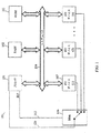
図4は、割込みコントローラ450の一部として優先順位付け器403を用いる多チャンネルの予め格納されたベクトル割込み処理システム400のブロック図である。図4では、システムバスの分離データバス408およびアドレスバス407部分が示される。プロセッサ409およびプログラム格納装置429は、データバス408およびアドレスバス407の両方に接続される。割込みベクトル格納装置406は、データバス408に接続される。割込みベクトル格納装置406に関連付けられたメモリマッピング位置にアドレスバスのコンテンツを分解する際に使用するためのアドレスバスから高次(p−n)ビットを受け取るために、セレクタ470の一部であるアドレスデコーダ405がアドレスバスに接続される。このアドレスバス407は、バスチャンネル427を介してマルチプレクサ404にさらに接続される。マルチプレクサ404は、以下にさらに説明されるように、通常割込み処理動作(割込みモード)とベクトル格納初期化(初期化モード)との間でシステム400をスイッチングする場合に支援する。セレクタ470は、割込みベクトル格納装置406に接続され、割込みベクトル格納装置406の読み出し/書き込み(R/W)入力にモード制御信号428を発行する。このセレクタは、制御信号451によって割込みベクトル格納装置406のCS_VS入力にさらに接続され、制御信号440によってプログラム格納装置429のCS_PS入力に接続される。複数の2n個までのI/Oデバイス401は、複数の2n個までの割込みリクエストライン402を介して優先順位付け器403に接続される。優先順位付け器403は、マルチプレクサ404への割込みソースを明確に識別するnビットのマルチビット優先順位付け割込みソース識別子信号410を出力する。サービス可能I/Oデバイス401の数と割込みソース識別子信号410の対応する好適なビット幅との間の関係は、n=log2mによって与えられ、mはサービス可能I/Oデバイスの最大数を表し、nは、割込みソース識別子信号410の大きさを切り上げたビットで表す。例えば、32個までのI/Oデバイス401に対して、nは5であり、16個までのI/Oデバイス401に対して、nは4に等しい。
【0022】
セレクタのアドレスデコードブロック405は、好ましくは、システム400において存在し得るかまたはそのシステム外部に存在し得る任意の他のアドレスデコーダの機能性から独立して存在する。予め格納されたベクトル割込み処理システムの外部にある改変されたチップ選択論理はまた、システムが初期化モードで動作する場合、好ましくは信号に供給される。例えば、プロセッサの現在の状態を規定するプロセッサ409内部のレジスタのセットは、この目的のためにセレクタ470に制御信号を供給し得る。これは、単に予め格納されたベクトル割込み処理システム400が初期化の開始の通知を提供することに依存し得る状態レジスタまたはフラグであり得る。同様な外部論理は、割込みベクトルがそのデバイスにロードされると同時に、他のデバイスがデータバス408に対して選択されないことを確実にすることに対して責任がある。
【0023】
ベクトル格納初期化(初期化モード)の間、割込みベクトル格納装置406のCS_VS入力は、制御信号451によって活性化され、割込みベクトル格納装置にデータバスの排他的な制御を与える。このセレクタはまた、初期化の間にプログラム格納装置429のCS_PS入力へのCS_Code制御信号が選択されないことを確実にしなければならない。初期化モード動作の一部として、アドレスデコーダおよびセレクタ470はまた、(1)書き込み(W)モードで割込みベクトル格納装置406を配置するように制御信号428を割込みベクトル格納装置406に発行する、および(2)マルチプレクサ404を初期化モードにするようにマルチプレクサ404にモード制御信号428を発行する。アドレスバスハイビット(p−n)を割込みベクトル格納装置のメモリマッピング位置に首尾よく分解することによって、マルチプレクサ404は、ロウビット(n)でアドレスバス407を通って、バスチャンネル427を介して割込みベクトル格納装置406に簡単に伝達させる。
【0024】
一方で初期化モードでは、アドレスバス407は、特定の割込みサービスルーチンのための特定の割込みベクトルに(分枝命令アドレスの形態で)対応するメモリアドレスを受信する。あるいは、一方で初期化モードでは、割込みベクトル格納装置406への書き込みを待って、データバス408は特定の割込みベクトル(すなわち、分枝命令オペレーション−コードおよびアドレス)を受信する。システム400は、割込みベクトルおよびそれに関連付けられたアドレスの全てにわたってサイクルして、割込みベクトル格納装置408にロードする。ロードはプロセッサ409または別のコントローラ(例えばDMAコントローラ)の制御の下で実行され得る。初期化は割込みベクトル格納装置408が各割込みルーチン分枝命令のコピーを保持する場合に終了する。
【0025】
予め格納されたベクトル割込み処理システムのコンポーネントとしてマルチプレクサ404の包含は、割込みベクトル格納装置406の初期化の他の方法が存在しない場合に限り必要である。予め格納されたベクトル割込み処理システムの一実施形態は、ROM(図3または図4に示されない)割込みベクトル格納装置406のインプリメンテーションを企図する。この場合、マルチプレクサ404は必要とされない。所定のチップ選択論理およびアドレス復号化機能性は、それに従って、マルチプレクサの欠如に適応するように改変される必要がある。
【0026】
予め格納されたベクトル割込み処理システム400が割込みベクトル格納装置406の初期化を終了する場合、システム400は、動作モード(割込みモード)にスイッチングする。一方で割込みモードでは、セレクタ470は、(1)マルチプレクサ404にモード制御信号428を発行して、マルチプレクサ404を割込みモードにし(従って、セレクタは、アドレスバス407ではなく、優先順位付け器403から割込みソース識別子410を介して伝達するように)、(2)割込みベクトル格納装置406にモード制御信号428を発行して、割込みベクトル格納装置406を読み出し(R)モードにする。いくつかの理由によって割込みベクトルがプログラムの実行の間に改変されない場合、割込みモードの間、通常情報は、書き込まれるのではなく、割込みベクトル格納装置406から読み出されるだけである。
【0027】
初期化および割込みモードの両方では、セレクタ470は、2つのデバイスの一方または他方によってデータバス408への排他的なアクセスを確実にすることに対して責任がある(割込みベクトル格納装置406とプログラム格納装置429デバイスのみとの間にある場合)。一実施形態では、セレクタは、AND、OR、またはNOTゲートを使用して、CS_PS信号およびCS_VS信号を割込みベクトル格納装置406またはプログラム格納装置429に送達するように単純なデジタル論理を使用する。従って、割込みベクトル格納装置へのCS_VS入力が制御信号451を介してアサートされる場合、セレクタは、制御信号440を介したプログラム格納装置429へのCS_PS入力がデアサートされることを確実にする。同様に、プログラム格納装置429へのCS_PS入力が制御信号440を介してアサートされる場合、セレクタは、割込みベクトル格納装置406へのCS_VS入力がデアサートされることを確実にする。この態様で、割込みベクトル格納装置およびプログラム格納装置はデータバスを同時に制御しない。
【0028】
分離R/W制御信号428および割込みベクトル格納装置406へのCS_VS制御信号451の入力は、予め格納されたベクトル割込み処理システムのこの実施形態において両方とも必要である。割込みベクトル格納装置406へのR/W制御信号は、割込みベクトル格納装置406が初期化モードにわたって書き込み(W)および割込みモードにわたって読み出し(R)をアサートしたままであることを確実にする。割込みベクトル格納装置406への分離CS_VS入力は、割込みベクトル格納装置406が、割込みモードおよび初期化モードの両方においてデータバス408の排他的制御を維持する。
【0029】
割込みモードでは、任意の割込みがない場合、プロセッサ409はプログラム格納装置429から読み出し、命令を実行する。この時点で、セレクタ470に接続されるプロセッサのサイクルタイプ出力信号435は、プロセッサ409が非割込み条件において動作することを示す状態で維持される。割込みが存在しない場合、セレクタ470が、プログラム格納装置429にアサートされたチップ選択信号440を維持し、割込みベクトル格納装置406にデアサートされた割込みリクエストチップ選択信号451を維持する。
【0030】
優先順位付け器403は時折、複数の割り込みリクエストライン402を介してI/Oデバイス401から割り込みリクエストを受け取る。割り込みモード中に割り込みが起こると、マスタ割り込みリクエスト信号436が優先順位付け器403からプロセッサ409にアサートされ、プロセッサ409はこれに応答して現在の命令を終えてサイクルタイプ信号435およびR/W信号444をアサートする。サイクルタイプ信号435およびR/W信号444は両方ともセレクタ470に接続されている。セレクタ470は上記(図3に示す実施形態)同様、プロセッサの命令フェッチサイクルタイプ信号ならびにプロセッサのR/W出力信号およびアドレスを妨害し、プログラム記憶装置429を非選択にし割り込みベクトル記憶装置406を選択することにより、割り込みベクトル(ブランチ命令オペコードおよびアドレス)が直接プロセッサ409にロードされるようにする。優先順位付け器403は、マスタ割り込みリクエスト信号436を生成することに加えて、起こった割り込み(あるいは複数の割り込みの場合は、優先順位の最も高い割り込み)に基づき割り込み識別信号410を生成することにより適切なベクトルを識別する。割り込み識別信号410はマルチプレクサ404を通過して割り込みベクトル記憶装置406に達し、割り込みベクトル記憶装置406からの対応する割り込みベクトルをデータバス408に強制的に送る。より特定すると、セレクタ470は、割り込みベクトル記憶装置406を選択して、その内容をデータバス408上で使用可能にする。プロセッサ409がサイクルタイプ信号435をアサートすると、次の割り込みベクトル(ブランチ命令オペコードおよびアドレス)が予測され、そのためデータバス408からの割り込みベクトルがプロセッサ409の実行ユニット452に直接ロードされる。
【0031】
図3および図4の両方のシステムの特徴は、割り込み識別信号が実質的に、割り込み源の多ビット符号化識別を提供し、したがって割り込みベクトルの多ビット符号化識別を提供することである。割り込み識別信号は様々な実施形態において、直接割り込みベクトル記憶装置308または406に、対応する割り込みベクトルが見つけられるべきアドレスにおいて付与される。割り込み識別子と割り込みベクトル記憶装置内の割り込みベクトルの位置との間の直接的対応は、割り込みに応答する際に速度および効率の点で利点がある。
【0032】
図3を参照して述べたシステム300同様、図4のシステム400も様々な割り込み源をマスクする回路を含み得る。たとえば、割り込みマスクレジスタは、特定の割り込みが通過し得るか否かを示す個々のマスクビットを保持するために用いられ得る。各マスクビットは、マスクビットの状態に依存して対応する割り込み信号が通過することを可能にするゲート(たとえば、ANDゲートまたはNANDゲート)を制御し得る。マスキングは、ネスティングされてもよいしされなくてもよい。ネスティングされた場合、高層マスクビットが各々、低層マスクビットの指定されたグループを制御し得る。割り込みは、割り込みに対して特定の低層マスクビットおよび割り込みの指定されたグループ用の高層マスクビットの両方が適切に設定された場合にのみ、通過する。
【0033】
図5は、予め記憶されたベクトル割り込み処理システム、たとえば、図3または図4に示すシステムなどを組み込んだプロセッサベースのシステムが行う工程のフロー図を示す。第1の工程505では、アプリケーション用のプログラムコードがプログラム記憶装置(メモリ)にロードされる。次の工程510では、予め記憶されたベクトル割り込み処理システムが、一例として図4に示す実施形態で述べた初期化技術を用いて初期化される。工程510は、割り込みベクトル記憶装置がROMで実行された場合に随意である工程である。工程515において、プログラム実行が開始される。プログラム実行を図5に示す。一連のプログラム命令ブロックを「プログラム命令1」520、「プログラム命令2」525〜「プログラム命令N」585と示す。通常のプログラム実行中は、プロセッサの命令サイクルは、予め記憶されたベクトル割り込み処理システムが割り込みコントローラ530からのマスクされていないサービスリクエストを受け取ったときに割り込み込まれる。
【0034】
工程535において、割り込みコントローラは、プロセッサ540への割り込みリクエスト信号(IRQ)をアサートする前に割り込みの優先順位を付ける。割り込みをまず処理することは、レジスタのスタックダンプおよびスタックへのプログラムカウンタを必要とし得る。割り込みコントローラは、割り込みベクトル記憶装置を選択しプログラム格納装置を非選択にすることにより、工程550でプロセッサの命令フェッチバスサイクル動作を妨害する。工程555において、割り込みコントローラの識別子信号に対応するブランチ命令オペコードおよびアドレス(割り込みベクトル)は、プロセッサの実行ユニット560まで直接移動する。割り込みベクトル565の実行後、プロセッサによって実行される次の命令が、リクエストされた割り込みサービスルーチン570の第1の命令となる。工程570の割り込みサービスルーチンが完了すると、PCおよびレジスタの保存されたコンテンツがスタックから取り出され、プロセッサ命令サイクルが割り込まれた点でプログラム実行が再開される(580)。
【0035】
本願発明の各実施形態において、割り込みソースは、ハードディスクドライブなどのデータ格納デバイス、ビデオディスプレイモニタなどのデータ出力デバイス、タイマーなどの埋め込みハードウェアデバイス、またはキーパッドもしくはポインティングデバイスなどのデータ入力デバイスのいずれでもあり得る。これらのカテゴリのI/Oデバイスの各々は、前格納ベクトル割り込みハンドリングシステムによって得られる利点を享受し得る。本願発明およびその実施形態は、割り込みソースの性質および数とは独立に機能する。
【0036】
本明細書に記載の前格納ベクトル割り込みハンドリングシステムの実施形態はすべて、サイクルタイプ(C_type)信号を使用してプロセッサの現在のバスサイクルを認定するが、そのような信号の使用は本発明の必須要件ではない。サイクルタイプ信号は一般にプロセッサ上に見られ得、かつバスサイクル復号を容易にし得る。当業者は、図3および4に示すアドレスデコーダおよびセレクタがサイクルタイプ信号を生成しないプロセッサを使用するためには変更が必要であり得ることを理解する。これらの変更は、プロセッサによって異なる。
【0037】
さらに、当業者は、プロセッサに基づくシステムが十分に広く、コンピュータシステム、携帯電話などの無線通信デバイス、マイクロコントローラ、デジタル信号処理システム、または中央プロセッサを含む任意の割り込み駆動システムを含むことを理解する。本明細書に記載される種々の実施形態によるプロセッサは、例えば、汎用プロセッサ、専用アプリケーション用プロセッサ、デジタル信号プロセッサ(DSP)、または命令を処理するために使用される任意の他のタイプのプロセッサであり得る。
【0038】
本明細書に記載されるような種々の実施形態は、以下の理由により従来の割り込み方法よりも高速であると期待される。第一に、前格納ベクトル割り込みハンドリングシステムは従来の割り込みハンドリング方法よりも高速である。なぜなら、システムは、割り込みサービスルーチンをメモリに配置するために使用される従来の方法では時間のかかる検索によって遅延されるからである。第二に、割り込み待ち時間(latency)が小さくあり得る。なぜなら、前格納ベクトル割り込みハンドリングシステムはハードウェアで完全に実施されるが、割り込みサービスルーチンを検索する従来の方法は一般にソフトウェアに基づくからである。第三に、プロセッサ時間は割り込みサービスルーチンを検索する際に無駄にされない。なぜなら、前格納ベクトル割り込みハンドリングシステムはベクトル(分岐命令オペコードおよびアドレス)を割り込みベクトル格納から直接にプロセッサの実行部分に転送する。その結果、プロセッサが実行するまさに次の命令は、関連割り込みサービスルーチンの第1の命令である。
【0039】
前格納ベクトル割り込みハンドリングシステムは、プロセッサの独立、スケーラビリティ、およびネスティングを含むさらなる利点を提供する。前格納ベクトル割り込みハンドリングシステムは特定のプロセッサ命令セットとは独立に動作するので、システムは多くの異なるプロセッサを用いて使用され得る。さらに、システムは任意の数の割り込みリクエストソースに対してスケーラブルである。例えば、図4のシステムなどの優先順位付け器を組み込む前格納ベクトル割り込みハンドリングシステム設計において、割り込みネスティングは適切に優先順位付け器を構成することによって可能である。
【0040】
種々のコンポーネントが互いに接続されるように記載される種々の実施形態が本明細書中に記載されたが、用語「接続される」は直接または間接に接続されることを意味するように最も広い意味で使用される。例えば、当業者は、本明細書中に記載される種々のシステム、プロセスおよび装置の一般的な全体機能を変更することなく、種々の信号がマルチプレクサ、バッファまたは他の中間コンポーネントを介してルーティングされ得ることを理解する。したがって、他の要素またはコンポーネントを本明細書に記載の割り込みハンドリングシステムおよびプロセスの種々の実施例に付与することも本発明の範囲内に完全に含まれることを意図する。
【0041】
本発明の好適な実施形態が本明細書中に記載されたが、本発明の概念および範囲内にある多くの変形例が可能である。そのような変形例は本明細書および図面を読んだ当業者にとって明らかである。したがって、本発明は特許請求の範囲に限定される。
【図面の簡単な説明】
【図1】 図1は、割込みを処理するポーリング方法を用いるプロセッサベースのシステムを示すブロック図である。
【図2】 図2は、割込みを処理する割込み方法を用いるプロセッサベースのシステムを示すブロック図である。
【図3】 図3は、本明細書中で開示されたような一実施形態によるセレクタを用いる予め格納されたベクトル処理システムのブロック図である。
【図4】 図4は、本明細書中で開示されたような別の実施形態による優先順位付け器を用いる予め格納されたベクトル割込み処理システムのブロック図である。
【図5】 図5は、本明細書中で開示されたような一実施形態による割込み処理のための方法のステップを示すフローチャートである。[0001]
(Field of Invention)
The field of the invention relates generally to processor-based systems, and more particularly to methods and systems for vectored interrupt handling in processor-based systems.
[0002]
(background)
Processor-based systems use peripheral components (called input / output (I / O devices)) to communicate with the external environment. Perhaps the best known processor-based system is a digital computer. Examples of I / O devices found in computer systems include keyboards, monitors, disk drives, and network interface cards, to name a few. An I / O device that requires attention typically sends several types of I / O service requests to the processor.
[0003]
For most applications, the speed and efficiency with which the system processes I / O requests is one of the major decisions on overall system throughput. Thus, a typical single processor system generally allocates processor time between each of the system's I / O devices when each of the I / O devices periodically needs attention from the processor. There must be several ways. The dominant method for providing these requests is polling and interrupt control.
[0004]
FIG. 1 is a block diagram functionally representing a processor-based
[0005]
FIG. 2 is a block diagram functionally illustrating an interrupt control method for processing an I / O service request.
[0006]
Prioritization is a means of hierarchically arranging the order of interrupt processing by a processor when one or more I / O devices request services either simultaneously or sequentially. The system establishes priorities by either hardware or software. Some computer systems establish hardware priorities by physical placement of I / O devices along the backplane. Thus, the physical placement of devices on the backplane corresponds to the level of the hierarchy. For example, higher priority I / O devices are placed physically close to the processor, while lower priority I / O devices are placed near the end of the device chain (and even outside the backplane). Is done.
[0007]
In addition to prioritization, the PIC masks interrupt signals to the processor. Masking is used for dynamic control where interrupts are serviceable. For those applications where interrupts are undesirable, service requests are temporarily disabled. However, some interrupts are not maskable (such as a power failure). In some systems, service requests issued while interrupts are disabled can be saved for processing after interrupts are re-enabled.
[0008]
Referring back to the example of a conventional system as shown in FIG. 2, after masking and priority establishment, the
[0009]
Common implementations of interrupt control methods include “vectorized” interrupts, which allow the processor to know which device issued the interrupt request. In this respect, a vector is an address or pointer to the corresponding ISR. When the processor receives an IRQ from the PIC, the processor searches the memory for the vector corresponding to the branch instruction associated with the ISR for the particular device.
[0010]
With respect to polling and interrupt control techniques, the processor must temporarily suspend execution of the current program in order to perform ISR. The processor first suspends the current program instruction and then saves the current state of the register bank (including the program counter (PC)) in a memory stack location known as a process control block. At the end of the ISR, the registers and PC values are restored from the process control block and program execution continues with the instruction located at the memory address originally held by the PC before the interrupt. In this way, the processor can meet the above-mentioned need to allocate that time between several I / O devices.
[0011]
Both polling and interrupt control techniques utilize the processor to search for interrupt sources. Each method is insufficient and wasteful in its own relationship. Polling methods cause potentially significant damage to system throughput by wasting processor time looping through the polling cycle. Typically, interrupt control methods typically read interrupt data (eg, flags or data registers) from the PIC and identify fault sources that often involve parsing the provided data. Use an adequate software search process. In both methods, the overhead of parsing the data provided by the PIC increases as more interrupt sources are provided to the system. Once the source is determined, the processor eventually branches to the ISR and the ISR is executed.
[0012]
The software retrieval routine used by the interrupt control method introduces an unnecessary delay between the assertion of the interrupt and the start of execution of the appropriate ISR. This delay can be particularly apparent in systems with tens or hundreds of interrupts. In some real-time systems (especially digital signal processors found in wireless telephones), this delay represents a substantial burden on efficient signal processing. Therefore, it would be advantageous to provide a faster and more efficient technology for other components that require service in multiple I / O devices or processor-based systems.
[0013]
(Summary of the Invention)
In one aspect, the present invention relates to a system and method for handling interrupts in a processor-based system. In certain embodiments, processor branch instructions are stored as vectors in a vector store. Each vector corresponds to an interrupt service routine in memory. When an event occurs, the pre-stored vector interrupt handling system executes using a vector from the vector store instead of an instruction from memory each time the processor receives an instruction fetch cycle in response to an IRQ input Load the unit. The processor then quickly and efficiently branches to the location specified by the vector and executes the corresponding interrupt service routine.
[0014]
Direct vector delivery provides system reduced interrupt processing delay by avoiding software intensive search routines. In processor-based systems that include a large number of interrupts, the overhead savings realized by the pre-stored vector interrupt processing system can be important. In an aspect of the invention, the interrupt vector includes a complete branch instruction, which includes a branch operation code and a target address.
[0015]
(Detailed description of preferred embodiments)
FIG. 3 is a block diagram of one embodiment of a pre-processed vector interrupt processing system. As shown in FIG. 3, the plurality of I /
[0016]
In operation, if a service is requested by one of the I /
[0017]
The execution unit of a processor often includes an instruction fetcher, instruction decoder, arithmetic / logic unit (ALU), program counter, and other components that are potentially dependent on the complexity of the processor. In an embodiment of the pre-stored vector interrupt processing system, the branch instruction operation-code and address are delivered by the interrupt
[0018]
Prestored vector interrupt
[0019]
Another embodiment of a pre-stored vector interrupt handling system that incorporates one or more concepts of the system of FIG. 3 includes a prioritizer within the interrupt control element. The prioritizer may prioritize a plurality of interrupt request signals input to the interrupt control device prior to processing. In addition, if the pre-stored vector interrupt processing system intercepts the processor's normal instruction fetch cycle type signal, the prioritizer interrupts the interrupt identifier signal to identify which interrupt vector is output. It can be configured to assert to the vector store. The prioritizer may be particularly available in two states. (1) if more than one I / O device requests service simultaneously, or (2) if the I / O device is more urgent than the urgency of a lower priority interrupt request that is currently being processed ( (Higher priority) request is issued. In the second situation, it is shown that lower priority interrupt requests are nested within higher priority interrupt requests. Nested interrupt handling is processor dependent. Thus, while the prioritizer may have no difficulty in issuing multiple simultaneous (ie, nested) interrupts of various priorities, each processor may have these nested interrupts in a different manner. Designed or configured to receive and process Alternatively, once the initial interrupt request is initiated, several processors mask out subsequent interrupt request signals from the prioritizer, thereby disabling nested or prioritized interrupt processing from each other. Can be.
[0020]
The pre-stored vector interrupt handling system is processor dependent. In addition, many microprocessors include elements such as cache RAMs, which may require changes in prestored vector interrupt processing system operation. The pre-stored vector interrupt processing circuit should be arranged so that interrupt vectors are not stored in the instruction cache. For example, if the
[0021]
FIG. 4 is a block diagram of a multi-channel pre-stored vector interrupt
[0022]
The selector's
[0023]
During vector store initialization (initialization mode), the CS_VS input of interrupt
[0024]
On the other hand, in initialization mode, the
[0025]
Inclusion of
[0026]
When the pre-stored vector interrupt
[0027]
In both initialization and interrupt modes,
[0028]
The separation R /
[0029]
In the interrupt mode, when there is no arbitrary interrupt, the
[0030]
The
[0031]
A feature of both the systems of FIGS. 3 and 4 is that the interrupt identification signal substantially provides a multi-bit encoded identification of the interrupt source, and thus provides a multi-bit encoded identification of the interrupt vector. The interrupt identification signal, in various embodiments, is provided directly to the interrupt
[0032]
Similar to the
[0033]
FIG. 5 shows a flow diagram of the steps performed by a pre-stored vector interrupt handling system, such as a processor-based system incorporating the system shown in FIG. 3 or FIG. In a
[0034]
In
[0035]
In each embodiment of the present invention, the interrupt source is any of a data storage device such as a hard disk drive, a data output device such as a video display monitor, an embedded hardware device such as a timer, or a data input device such as a keypad or pointing device. But it can be. Each of these categories of I / O devices can benefit from the prestored vector interrupt handling system. The present invention and its embodiments function independently of the nature and number of interrupt sources.
[0036]
Although all of the embodiments of the prestored vector interrupt handling system described herein use a cycle type (C_type) signal to qualify the processor's current bus cycle, the use of such a signal is essential to the invention. It is not a requirement. Cycle type signals can generally be found on the processor and can facilitate bus cycle decoding. Those skilled in the art will appreciate that the address decoder and selector shown in FIGS. 3 and 4 may require modification to use a processor that does not generate cycle type signals. These changes depend on the processor.
[0037]
Furthermore, those skilled in the art will appreciate that processor-based systems are sufficiently broad to include any interrupt driven system including a computer system, a wireless communication device such as a mobile phone, a microcontroller, a digital signal processing system, or a central processor. . A processor according to various embodiments described herein may be, for example, a general purpose processor, a dedicated application processor, a digital signal processor (DSP), or any other type of processor used to process instructions. possible.
[0038]
Various embodiments as described herein are expected to be faster than conventional interrupt methods for the following reasons. First, the pre-stored vector interrupt handling system is faster than conventional interrupt handling methods. This is because the system is delayed by time consuming searches in the conventional method used to place interrupt service routines in memory. Second, the interrupt latency can be small. This is because the pre-stored vector interrupt handling system is fully implemented in hardware, but conventional methods of retrieving interrupt service routines are generally software based. Third, processor time is not wasted when searching for interrupt service routines. This is because the pre-stored vector interrupt handling system transfers vectors (branch instruction opcode and address) directly from the interrupt vector store to the execution part of the processor. As a result, the very next instruction that the processor executes is the first instruction of the associated interrupt service routine.
[0039]
The prestored vector interrupt handling system provides further advantages including processor independence, scalability, and nesting. Since the prestored vector interrupt handling system operates independently of a particular processor instruction set, the system can be used with many different processors. Furthermore, the system is scalable for any number of interrupt request sources. For example, in a pre-stored vector interrupt handling system design that incorporates a prioritizer such as the system of FIG. 4, interrupt nesting is possible by configuring the prioritizer appropriately.
[0040]
Various embodiments have been described herein in which various components are described as being connected to each other, but the term “connected” is broadest to mean connected directly or indirectly Used in meaning. For example, one of ordinary skill in the art will be able to route various signals through a multiplexer, buffer, or other intermediate component without changing the general overall functionality of the various systems, processes, and devices described herein. Understand what you get. Accordingly, the provision of other elements or components to the various embodiments of the interrupt handling systems and processes described herein is intended to be fully included within the scope of the present invention.
[0041]
While preferred embodiments of the invention have been described herein, many variations are possible which are within the concept and scope of the invention. Such variations will be apparent to those skilled in the art after reading this specification and the drawings. Accordingly, the invention is limited only by the following claims.
[Brief description of the drawings]
FIG. 1 is a block diagram illustrating a processor-based system using a polling method for handling interrupts.
FIG. 2 is a block diagram illustrating a processor-based system using an interrupt method for handling interrupts.
FIG. 3 is a block diagram of a pre-stored vector processing system using a selector according to one embodiment as disclosed herein.
FIG. 4 is a block diagram of a pre-stored vector interrupt handling system using a prioritizer according to another embodiment as disclosed herein.
FIG. 5 is a flowchart illustrating method steps for interrupt handling according to one embodiment as disclosed herein.
Claims (12)
複数の割込ベクトルを含む割込ベクトル記憶装置と、
複数の割込リクエスト信号に接続された割込制御デバイスであって、該割込制御デバイスは、割込リクエスト信号を該プロセッサに出力する、割込制御デバイスと、
該プロセッサのサイクルタイプ信号に応答して、該プロセッサの実行ユニットに直接的にロードされるように、該プログラム記憶装置からのプログラムコード命令と該割込ベクトル記憶装置からの割込ベクトルとの間で選択を行うセレクタと
を含む、予め格納されたベクトルの割込処理システム。 In a system having a processor configured to execute the program code instructions stored in the program memory, a interrupt processing of pre-stored vector,
An interrupt vector storage device including a plurality of interrupt vectors;
An interrupt control device connected to a plurality of interrupt request signals, the interrupt control device outputting an interrupt request signal to the processor;
In response to a cycle type signal of the processor, between a program code instruction from the program store and an interrupt vector from the interrupt vector store to be loaded directly into the execution unit of the processor A pre-stored vector interrupt processing system, including a selector that performs selection at.
Applications Claiming Priority (2)
| Application Number | Priority Date | Filing Date | Title |
|---|---|---|---|
| US09/735,266 US6889279B2 (en) | 2000-12-11 | 2000-12-11 | Pre-stored vector interrupt handling system and method |
| PCT/US2001/048027 WO2002048882A1 (en) | 2000-12-11 | 2001-12-11 | Pre-stored vector interrupt handling system and method |
Publications (3)
| Publication Number | Publication Date |
|---|---|
| JP2004516548A JP2004516548A (en) | 2004-06-03 |
| JP2004516548A5 JP2004516548A5 (en) | 2005-04-21 |
| JP4057911B2 true JP4057911B2 (en) | 2008-03-05 |
Family
ID=24955044
Family Applications (1)
| Application Number | Title | Priority Date | Filing Date |
|---|---|---|---|
| JP2002550526A Expired - Fee Related JP4057911B2 (en) | 2000-12-11 | 2001-12-11 | Pre-stored vector interrupt processing system and method |
Country Status (5)
| Country | Link |
|---|---|
| US (1) | US6889279B2 (en) |
| EP (1) | EP1344130A4 (en) |
| JP (1) | JP4057911B2 (en) |
| AU (1) | AU2002232557A1 (en) |
| WO (1) | WO2002048882A1 (en) |
Families Citing this family (22)
| Publication number | Priority date | Publication date | Assignee | Title |
|---|---|---|---|---|
| US6865663B2 (en) * | 2000-02-24 | 2005-03-08 | Pts Corporation | Control processor dynamically loading shadow instruction register associated with memory entry of coprocessor in flexible coupling mode |
| US7487339B2 (en) * | 2001-10-12 | 2009-02-03 | Mips Technologies, Inc. | Method and apparatus for binding shadow registers to vectored interrupts |
| JP4079653B2 (en) * | 2002-02-22 | 2008-04-23 | 三洋電機株式会社 | Clock control method and clock control circuit |
| US20030204655A1 (en) * | 2002-04-24 | 2003-10-30 | Schmisseur Mark A. | Prioritizing vector generation in interrupt controllers |
| US20050033889A1 (en) * | 2002-10-08 | 2005-02-10 | Hass David T. | Advanced processor with interrupt delivery mechanism for multi-threaded multi-CPU system on a chip |
| US7117284B2 (en) * | 2002-11-18 | 2006-10-03 | Arm Limited | Vectored interrupt control within a system having a secure domain and a non-secure domain |
| US20050165990A1 (en) * | 2003-01-24 | 2005-07-28 | Fujitsu Limited | Interrupt control device |
| TW591525B (en) * | 2003-03-07 | 2004-06-11 | Novatek Microelectronics Corp | Interrupt-processing system for shortening interrupt latency in microprocessor |
| US7243178B2 (en) * | 2003-05-16 | 2007-07-10 | Intel Corporation | Enable/disable claiming of a DMA request interrupt |
| CN100367136C (en) * | 2004-02-17 | 2008-02-06 | 联想(北京)有限公司 | Universal control method |
| DE102005009874B4 (en) * | 2005-03-01 | 2010-04-15 | Infineon Technologies Ag | Method for signaling a state or event |
| US7363409B2 (en) * | 2006-02-08 | 2008-04-22 | Texas Instruments Incorporated | Interrupt control system and method for reducing interrupt latency |
| US7424563B2 (en) * | 2006-02-24 | 2008-09-09 | Qualcomm Incorporated | Two-level interrupt service routine |
| US7849247B2 (en) * | 2008-10-14 | 2010-12-07 | Freescale Semiconductor, Inc. | Interrupt controller for accelerated interrupt handling in a data processing system and method thereof |
| JP5267328B2 (en) * | 2009-05-26 | 2013-08-21 | 富士通セミコンダクター株式会社 | Interrupt notification control device and semiconductor integrated circuit |
| US9378164B2 (en) | 2011-12-22 | 2016-06-28 | Intel Corporation | Interrupt return instruction with embedded interrupt service functionality |
| CN103186435B (en) * | 2011-12-28 | 2015-11-25 | 英业达股份有限公司 | System mistake disposal route and the server system using the method |
| KR101642211B1 (en) | 2012-03-28 | 2016-07-22 | 인텔 코포레이션 | Method for implementing secure data channel between processor and devices |
| DE102017108219A1 (en) | 2017-04-18 | 2018-10-18 | Infineon Technologies Ag | Control system and method of memory access |
| DE102017108216A1 (en) * | 2017-04-18 | 2018-10-18 | Infineon Technologies Ag | Control system and method of memory access |
| CN111078387B (en) * | 2017-12-25 | 2024-01-23 | 贵阳忆芯科技有限公司 | Interrupt aggregation device and method thereof |
| JP6955163B2 (en) * | 2017-12-26 | 2021-10-27 | 富士通株式会社 | Information processing equipment, information processing methods and programs |
Family Cites Families (20)
| Publication number | Priority date | Publication date | Assignee | Title |
|---|---|---|---|---|
| US4037204A (en) * | 1974-10-30 | 1977-07-19 | Motorola, Inc. | Microprocessor interrupt logic |
| US5854907A (en) * | 1982-02-22 | 1998-12-29 | Texas Instruments Incorporated | Microcomputer for digital signal processing having on-chip memory and external memory access |
| US4709324A (en) * | 1985-11-27 | 1987-11-24 | Motorola, Inc. | Data processor control unit having an interrupt service using instruction prefetch redirection |
| DE69230554T2 (en) * | 1991-07-08 | 2000-07-06 | Seiko Epson Corp | RISC MICROPROCESSOR ARCHITECTURE WITH FAST INTERRUPT AND EXCEPTION MODE |
| JPH05233318A (en) * | 1992-02-18 | 1993-09-10 | Nec Corp | Microprocessor |
| US5473763A (en) * | 1993-08-02 | 1995-12-05 | Advanced Micro Devices, Inc. | Interrupt vector method and apparatus |
| US5511200A (en) | 1993-12-01 | 1996-04-23 | Intel Corporation | Method and apparatus for providing an enhanced programmable priority interrupt controller |
| US6161208A (en) * | 1994-05-06 | 2000-12-12 | International Business Machines Corporation | Storage subsystem including an error correcting cache and means for performing memory to memory transfers |
| US5608886A (en) * | 1994-08-31 | 1997-03-04 | Exponential Technology, Inc. | Block-based branch prediction using a target finder array storing target sub-addresses |
| US6067407A (en) * | 1995-06-30 | 2000-05-23 | Canon Information Systems, Inc. | Remote diagnosis of network device over a local area network |
| CA2159979C (en) * | 1995-10-05 | 1999-05-25 | Arthur Lai | Methology to link any pci rom based device using a single software or hardware interrupt vector in pc system at runtime |
| US5903749A (en) * | 1996-07-02 | 1999-05-11 | Institute For The Development Of Emerging Architecture, L.L.C. | Method and apparatus for implementing check instructions that allow for the reuse of memory conflict information if no memory conflict occurs |
| US6324608B1 (en) * | 1997-05-13 | 2001-11-27 | Micron Electronics | Method for hot swapping of network components |
| US6128728A (en) * | 1997-08-01 | 2000-10-03 | Micron Technology, Inc. | Virtual shadow registers and virtual register windows |
| US5901309A (en) * | 1997-10-07 | 1999-05-04 | Telefonaktiebolaget Lm Ericsson (Publ) | Method for improved interrupt handling within a microprocessor |
| JPH11219299A (en) * | 1998-02-02 | 1999-08-10 | Mitsubishi Electric Corp | Microcomputer |
| JP2001005676A (en) * | 1999-06-18 | 2001-01-12 | Mitsubishi Electric Corp | Interruption processor |
| US6205509B1 (en) * | 1999-07-15 | 2001-03-20 | 3Com Corporation | Method for improving interrupt response time |
| US6917997B2 (en) * | 2000-06-29 | 2005-07-12 | Palmchip Corporation | Integrated circuit including interrupt controller with shared preamble execution and global-disable control bit |
| US6757771B2 (en) * | 2000-08-09 | 2004-06-29 | Advanced Micro Devices, Inc. | Stack switching mechanism in a computer system |
-
2000
- 2000-12-11 US US09/735,266 patent/US6889279B2/en not_active Expired - Fee Related
-
2001
- 2001-12-11 EP EP01992083A patent/EP1344130A4/en not_active Ceased
- 2001-12-11 WO PCT/US2001/048027 patent/WO2002048882A1/en active Application Filing
- 2001-12-11 AU AU2002232557A patent/AU2002232557A1/en not_active Abandoned
- 2001-12-11 JP JP2002550526A patent/JP4057911B2/en not_active Expired - Fee Related
Also Published As
| Publication number | Publication date |
|---|---|
| AU2002232557A1 (en) | 2002-06-24 |
| EP1344130A1 (en) | 2003-09-17 |
| US20020073262A1 (en) | 2002-06-13 |
| US6889279B2 (en) | 2005-05-03 |
| JP2004516548A (en) | 2004-06-03 |
| EP1344130A4 (en) | 2007-12-26 |
| WO2002048882A1 (en) | 2002-06-20 |
Similar Documents
| Publication | Publication Date | Title |
|---|---|---|
| JP4057911B2 (en) | Pre-stored vector interrupt processing system and method | |
| US7984281B2 (en) | Shared interrupt controller for a multi-threaded processor | |
| US8799929B2 (en) | Method and apparatus for bandwidth allocation mode switching based on relative priorities of the bandwidth allocation modes | |
| US6230259B1 (en) | Transparent extended state save | |
| KR102187912B1 (en) | Apparatus and method for configuring sets of interrupts | |
| JP2004520662A (en) | Selective access to multiple registers with common names | |
| US7111182B2 (en) | Thread scheduling mechanisms for processor resource power management | |
| US20100122064A1 (en) | Method for increasing configuration runtime of time-sliced configurations | |
| EP1760580B1 (en) | Processing operation information transfer control system and method | |
| WO2001038970A2 (en) | Buffer memories, methods and systems for buffering having seperate buffer memories for each of a plurality of tasks | |
| US5948093A (en) | Microprocessor including an interrupt polling unit configured to poll external devices for interrupts when said microprocessor is in a task switch state | |
| JP5289688B2 (en) | Processor system and operating system program processing method for operating processor system | |
| US20120072632A1 (en) | Deterministic and non-Deterministic Execution in One Processor | |
| US20060168428A1 (en) | Method of providing microcontroller context management | |
| JPH0916409A (en) | Microcomputer | |
| US5671424A (en) | Immediate system management interrupt source with associated reason register | |
| US20140136818A1 (en) | Fetch less instruction processing (flip) computer architecture for central processing units (cpu) | |
| KR100978147B1 (en) | Centralized interrupt controller | |
| GB2372348A (en) | A multi-mode, multi-tasking processor with reduction in context preservation and restoration to save processing time | |
| US20200319896A1 (en) | Dual wakeup interrupt controllers | |
| JP2011070290A (en) | Data processor | |
| US20140372733A1 (en) | Processor with inter-execution unit instruction issue | |
| US20230315456A1 (en) | Processing apparatus | |
| JPWO2004023291A1 (en) | Information processing equipment | |
| JPH10240702A (en) | Parallel processing processor and method therefor |
Legal Events
| Date | Code | Title | Description |
|---|---|---|---|
| A621 | Written request for application examination |
Free format text: JAPANESE INTERMEDIATE CODE: A621 Effective date: 20041209 |
|
| A977 | Report on retrieval |
Free format text: JAPANESE INTERMEDIATE CODE: A971007 Effective date: 20061228 |
|
| A131 | Notification of reasons for refusal |
Free format text: JAPANESE INTERMEDIATE CODE: A131 Effective date: 20070105 |
|
| A601 | Written request for extension of time |
Free format text: JAPANESE INTERMEDIATE CODE: A601 Effective date: 20070405 |
|
| A602 | Written permission of extension of time |
Free format text: JAPANESE INTERMEDIATE CODE: A602 Effective date: 20070420 |
|
| A521 | Request for written amendment filed |
Free format text: JAPANESE INTERMEDIATE CODE: A523 Effective date: 20070605 |
|
| TRDD | Decision of grant or rejection written | ||
| A01 | Written decision to grant a patent or to grant a registration (utility model) |
Free format text: JAPANESE INTERMEDIATE CODE: A01 Effective date: 20071119 |
|
| A61 | First payment of annual fees (during grant procedure) |
Free format text: JAPANESE INTERMEDIATE CODE: A61 Effective date: 20071214 |
|
| R150 | Certificate of patent or registration of utility model |
Free format text: JAPANESE INTERMEDIATE CODE: R150 |
|
| FPAY | Renewal fee payment (event date is renewal date of database) |
Free format text: PAYMENT UNTIL: 20101221 Year of fee payment: 3 |
|
| FPAY | Renewal fee payment (event date is renewal date of database) |
Free format text: PAYMENT UNTIL: 20111221 Year of fee payment: 4 |
|
| FPAY | Renewal fee payment (event date is renewal date of database) |
Free format text: PAYMENT UNTIL: 20121221 Year of fee payment: 5 |
|
| FPAY | Renewal fee payment (event date is renewal date of database) |
Free format text: PAYMENT UNTIL: 20121221 Year of fee payment: 5 |
|
| FPAY | Renewal fee payment (event date is renewal date of database) |
Free format text: PAYMENT UNTIL: 20131221 Year of fee payment: 6 |
|
| LAPS | Cancellation because of no payment of annual fees |