JP4057791B2 - PLL circuit and wireless communication terminal device - Google Patents
PLL circuit and wireless communication terminal device Download PDFInfo
- Publication number
- JP4057791B2 JP4057791B2 JP2001083973A JP2001083973A JP4057791B2 JP 4057791 B2 JP4057791 B2 JP 4057791B2 JP 2001083973 A JP2001083973 A JP 2001083973A JP 2001083973 A JP2001083973 A JP 2001083973A JP 4057791 B2 JP4057791 B2 JP 4057791B2
- Authority
- JP
- Japan
- Prior art keywords
- output
- constant current
- frequency
- switch
- phase comparator
- Prior art date
- Legal status (The legal status is an assumption and is not a legal conclusion. Google has not performed a legal analysis and makes no representation as to the accuracy of the status listed.)
- Expired - Lifetime
Links
- 238000004891 communication Methods 0.000 title claims description 15
- 230000010355 oscillation Effects 0.000 claims description 13
- 238000006243 chemical reaction Methods 0.000 claims description 10
- 230000007704 transition Effects 0.000 claims 10
- 238000007599 discharging Methods 0.000 abstract description 2
- 230000005540 biological transmission Effects 0.000 description 22
- 238000010586 diagram Methods 0.000 description 19
- 238000000034 method Methods 0.000 description 6
- 239000003990 capacitor Substances 0.000 description 4
- 230000035945 sensitivity Effects 0.000 description 4
- 230000007423 decrease Effects 0.000 description 3
- 230000000694 effects Effects 0.000 description 3
- 101150110971 CIN7 gene Proteins 0.000 description 2
- 101100286980 Daucus carota INV2 gene Proteins 0.000 description 2
- 101150110298 INV1 gene Proteins 0.000 description 2
- 101100397044 Xenopus laevis invs-a gene Proteins 0.000 description 2
- 101100397045 Xenopus laevis invs-b gene Proteins 0.000 description 2
- 238000009825 accumulation Methods 0.000 description 2
- 238000013459 approach Methods 0.000 description 2
- 238000010295 mobile communication Methods 0.000 description 2
- 230000005236 sound signal Effects 0.000 description 2
- 239000013078 crystal Substances 0.000 description 1
- 238000012986 modification Methods 0.000 description 1
- 230000004048 modification Effects 0.000 description 1
- 230000000630 rising effect Effects 0.000 description 1
- 230000001629 suppression Effects 0.000 description 1
Images


Classifications
-
- H—ELECTRICITY
- H03—ELECTRONIC CIRCUITRY
- H03L—AUTOMATIC CONTROL, STARTING, SYNCHRONISATION OR STABILISATION OF GENERATORS OF ELECTRONIC OSCILLATIONS OR PULSES
- H03L7/00—Automatic control of frequency or phase; Synchronisation
- H03L7/06—Automatic control of frequency or phase; Synchronisation using a reference signal applied to a frequency- or phase-locked loop
- H03L7/08—Details of the phase-locked loop
- H03L7/085—Details of the phase-locked loop concerning mainly the frequency- or phase-detection arrangement including the filtering or amplification of its output signal
-
- H—ELECTRICITY
- H03—ELECTRONIC CIRCUITRY
- H03L—AUTOMATIC CONTROL, STARTING, SYNCHRONISATION OR STABILISATION OF GENERATORS OF ELECTRONIC OSCILLATIONS OR PULSES
- H03L7/00—Automatic control of frequency or phase; Synchronisation
- H03L7/06—Automatic control of frequency or phase; Synchronisation using a reference signal applied to a frequency- or phase-locked loop
- H03L7/07—Automatic control of frequency or phase; Synchronisation using a reference signal applied to a frequency- or phase-locked loop using several loops, e.g. for redundant clock signal generation
-
- H—ELECTRICITY
- H03—ELECTRONIC CIRCUITRY
- H03L—AUTOMATIC CONTROL, STARTING, SYNCHRONISATION OR STABILISATION OF GENERATORS OF ELECTRONIC OSCILLATIONS OR PULSES
- H03L7/00—Automatic control of frequency or phase; Synchronisation
- H03L7/06—Automatic control of frequency or phase; Synchronisation using a reference signal applied to a frequency- or phase-locked loop
- H03L7/08—Details of the phase-locked loop
- H03L7/10—Details of the phase-locked loop for assuring initial synchronisation or for broadening the capture range
- H03L7/104—Details of the phase-locked loop for assuring initial synchronisation or for broadening the capture range using an additional signal from outside the loop for setting or controlling a parameter in the loop
-
- H—ELECTRICITY
- H03—ELECTRONIC CIRCUITRY
- H03L—AUTOMATIC CONTROL, STARTING, SYNCHRONISATION OR STABILISATION OF GENERATORS OF ELECTRONIC OSCILLATIONS OR PULSES
- H03L2207/00—Indexing scheme relating to automatic control of frequency or phase and to synchronisation
- H03L2207/12—Indirect frequency synthesis using a mixer in the phase-locked loop
Landscapes
- Stabilization Of Oscillater, Synchronisation, Frequency Synthesizers (AREA)
- Digital Transmission Methods That Use Modulated Carrier Waves (AREA)
- Transceivers (AREA)
Abstract
Description
【0001】
【発明の属する技術分野】
本発明は、IF(中間周波数)信号をRF(無線周波数)信号に周波数変換するPLL回路の収束の高速化に適用して有効な技術に関する。
【0002】
【従来の技術】
移動体通信端末に用いられる送信機にはいくつかの方式が存在する。もっとも一般的なものは、ベースバンド信号を変調器でIF(中間周波数)信号に変換し、それをアンテナから送信すべき周波数にミキサで変換するミキサ方式である。この他に、該方式のミキサの替わりにPLL回路を用いて周波数変換するPLL方式がある。PLL方式は、定振幅変調しか扱えないという欠点はあるものの、送信雑音をミキサ方式に比べて大幅に低減できるという特長があり、主にGSM(Global System for Mobile communications)システムの無線通信端末機器に用いられている。その動作原理の詳細は、例えば、IEEE journal of solid-state circuits Vol. 32, No. 12, pp. 2089 - 2096, "A 2.7-V GSM RF Transceiver IC"に記されている。
【0003】
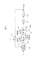
図12は、該PLL方式で用いられるPLL回路の一例を示した図である。該PLL回路は、電流出力型位相比較器100と、定電流源101と、ミキサ105と、低域通過フィルタ(LPF)103と、電圧制御発振器104と、スイッチ(SW)102とから構成される。以下の説明において、VCO104は正の感度をもつものと仮定する。LPF103には、一般に、図12に示す様な受動素子から成る2次LPFが使用される。また、SW102には制御信号LOGIC1が与えられる。LOGIC1が0の場合にSW102は開放状態となり、LOGIC1が1の場合にSW102はグランドに短絡する。
【0004】
電流出力型位相比較器100には、位相周波数比較器ではなく、高速動作可能なミキサ型の位相比較器が用いられる。これにより、送信機の周波数構成の自由度を上げることができる。位相比較器の欠点は、2つの入力の周波数差が大きい場合に、出力電圧がLPF103によって抑圧されVCO104に伝わらないということである。つまり、収束初期段階でのVCO104の出力周波数によっては該PLL回路が収束することができない。この欠点を解消するために、定電流源101とSW102が接続されている。該PLL回路が収束する前に必ずSW102をグランドに接続しVCO104の入力電位をグランド電位に設定する。その後、SW102を開放して収束を開始する。電流出力型位相比較器100の出力がVCO104に伝わらない場合でも、定電流源101がLPF103の容量を充電することにより、VCO104の入力電位が上昇する。これにより、電流出力型位相比較器100の2つの入力周波数は近づいていくことができる。該入力周波数が十分近づくと、電流出力型位相比較器100の出力がVCO104の入力に伝わり、収束が可能となる。
【0005】
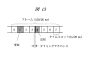
GSMシステムにはTDMA(Time Division Multiple Access) 方式が用いられている。1フレームは120/26msで、15/26msの8つのタイムスロットから構成される。1スロットを受信に、他の1スロットを送信に使用する。図13は、端末の送受信タイミングを示した一例である。この例では、タイムスロット1を受信に、タイムスロット4を送信に割り当てている。送受信間隔は2つのタイムスロット分である。ただし、端末から基地局への伝播遅延を考慮にいれ、送信は最大3024/13μsのタイミングアドバンス分早く行われる。
【0006】
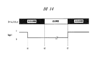
前記PLL方式が、前述のGSMのTDMA動作に従いどのように動作するかを、前記の従来のPLL回路と、図14に示すタイミングチャートを用いて説明する。説明の便宜のため、電流出力型位相比較器100の入力の中心周波数を270MHz、ミキサ105に入力される局発信号LOの周波数を1180MHzとする。また、VCO104の入力感度は正であり、入力電位が0Vの時の出力周波数を850MHzとする。端末が送信タイミングにない場合、LOGIC1には1が入力され、電流出力型位相比較器100の出力が0Vとなる。これにより、LPF103の容量に蓄積された電荷が放電され、VCO104の入力電位もまた0Vとなる。したがって、VCO104の出力周波数は850MHzとなる。時刻t1になると、LOGIC1には0が入力され、SW102は開放状態となる。この時のミキサ105の出力周波数は、850MHzと1180MHzの和と差、すなわち、2030MHzと330MHzである。和成分は、LPF103で抑圧され収束に寄与しないので、ここでは差成分のみを考える。したがって、電流出力型位相比較器100の出力周波数は、330−270=60MHzとなる。GSMシステムに用いる場合、一般に該PLL回路の帯域は約1MHzに設計されるので、ミキサ105の出力信号はLPF103で十分抑圧され、前記容量への電荷蓄積に寄与しない。つまり、フィードバックが切れた状態となる。しかし、定電流源101からの定電流により該容量に電荷が蓄積され、VCO104の入力電位は上昇する。その結果、VCO104の出力周波数は850MHzから上昇していく。VCO104の出力周波数が、例えば、908MHzに上昇した場合を考える。この時、電流出力型位相比較器100の出力周波数は2MHzとなる。したがって、LPF103での抑圧度が減少し、前記容量への電荷蓄積に寄与することができる。すなわち、フィードバックが回復する。フィードバックが回復したことにより、該PLL回路は最終的に収束し、VCO104の出力周波数は、1180−270=910MHzとなる。収束は、送信期間の始まる時刻t2よりも早く完了しなければならない。送信期間が終了する時刻t3に、LOGIC1には1が入力され、再びVCO104の入力電位を0Vとし、次の送信期間に備える。
【0007】
図15は、上記収束過程におけるVCO104の入力電位の変化を示した一例である。時刻t1までは、該入力電位は0Vである。時刻t1にSW102が開放となり、該入力電位が直線的に上昇を始める。該上昇の傾きは、主に定電流源101の出力電流I1と、LPF103の総容量Cにより決まり、I1/Cで与えられる。その後、フィードバックを回復し収束を完了する。VCO104の感度をKv、該入力電位が0V時のVCO104の出力周波数をf0、収束時のVCO104の出力周波数をf1とすると、収束時の該入力電位V1は数式1で与えられる。
【0008】
V1=(f1−f0)/Kv ・・・(数式1)
該PLL回路の収束時間tsは、該出力電流I1によって該総容量CがV1に充電される時間で近似できるので、tsは数式2で与えられる。
【0009】
ts=(f1−f0)/Kv・C/I1 ・・・(数式2)
したがって、f1が高いほど収束時間が長くなる。例えばGSMシステムでは、送信周波数の最高周波数915MHzに収束するときにもっとも収束時間が長くなる。
【0010】
近年、高速データ通信サービスの要求が急速に高まってきた。それに伴い、GSMシステムにおいても従来のデータレートを改善する方式がいくつか提案され、実用に向け検討が行われている。その一つがGPRS(General Packet Radio Service)である。GPRSは、図16に示すように複数のタイムスロットを送信または受信に割り当てることでデータレートを高める方式である。図13と図16を比較すれば明らかなように、GPRSでは前記PLL回路が収束に使える時間が従来のGSMに比べ約半分である。そこで、前記PLL回路の収束時間を短縮する必要がでてきた。
【0011】
【発明が解決しようとする課題】
前述の様に、従来のPLL回路の収束時間tsは数式2で与えられる。tsを短縮するには、数式2に含まれるパラメータを変更する必要がある。一般に、VCO104はモジュール部品として供給されるため、その特性値、f0とKvは固定値である。また、I1/Cは以下の1)2)に示す制限により自由に変更することが困難である。1)電流出力型位相比較器100の出力電流とCの比は、システムパラメータである変調帯域幅や許容雑音量によって決定される。2)該出力電流とI1の比により該PLL回路の収束安定性が決まる。つまり、従来のPLL回路の場合、前述の制限を満たしながら、収束時間を短縮することは困難である。
【0012】
そこで、本発明の目的は、前述の制限を満たしながら、従来のPLL回路の最大収束時間を短縮することである。
【0013】
本発明の前記ならびにその他の目的と新規な特徴は、本明細書の記述および添付図面から明らかになるであろう。
【0014】
【課題を解決するための手段】
本願において開示される発明のうち、代表的なものの概要を簡単に説明すれば、次のとおりである。
【0015】
上記目的を達成するために、本発明のPLL回路は、少なくとも電流出力型位相比較器と、低域通過フィルタと、VCOとを含むPLL回路であって、収束開始前には該VCOの入力電位を0Vとし、該PLL回路の収束周波数が設定周波数よりも低い場合には、該入力電位を0Vから収束電位までPLLフィードバックループにより収束させ、該収束周波数が該設定周波数よりも高い場合には、まず該入力電位を0Vから電源電圧まで該PLLフィードバックループを使わずに上昇させ、その後、該入力電位を該電源電圧から収束電位まで該PLLフィードバックループにより収束させるものである。
【0016】
また、上記目的を達成するための他の動作として、本発明のPLL回路は、少なくとも電流出力型位相比較器と、低域通過フィルタと、VCOとを含むPLL回路であって、収束開始前に該VCOの入力電位を電源電圧とし、該PLL回路の収束周波数が設定周波数よりも高い場合には、該入力電位を該電源電圧から収束電位までPLLフィードバックループにより収束させ、該収束周波数が該設定周波数よりも低い場合には、まず該入力電位を該電源電圧から0Vまで該PLLフィードバックループを使わずに下降させ、その後、該入力電位を0Vから収束電位まで該PLLフィードバックループにより収束させるものである。
【0017】
また、上記目的を達成するために、本発明のPLL回路の構成は、第1の入力信号と第2の入力信号の位相差に比例した信号を出力する電流出力型位相比較器と、該電流出力型位相比較器の出力端に接続されたLPFと、該LPFの出力端に接続されたVCOと、該VCOの出力端に接続され第2の信号を出力するミキサと、該電流出力型位相比較器の出力端に定電流を出力する第1と第2の定電流源と、該電流出力型位相比較器の出力端から定電流を吸収する第3の定電流源と、該電流出力型位相比較器とグランドとの間に接続された第1のスイッチとを有し、該第1、第2、第3の定電流源のオンオフと該第1のスイッチの開放、短絡を制御する手段を有するものである。
【0018】
また、上記目的を達成するための他の構成として、該本発明のPLL回路において、該第2の定電流源を該電流出力型位相比較器の出力端と電源電位との間に接続された第2のスイッチに置き換え、該第2のスイッチのオンオフを制御する手段を追加するものである。
【0019】
また、上記目的を達成するための他の構成として、該本発明のPLL回路において、該第1と第2の定電流源を可変電流源に置き換え、該可変電流源のオンオフと出力電流値を制御する手段を追加するものである。
【0020】
また、本発明の無線通信端末機器は、ベースバンド回路と、該ベースバンド回路から第1のベースバンド信号が入力される変調器と、該変調器の出力に接続されたPLL回路と、該PLL回路の出力に接続された電力増幅器と、該ベースバンド回路に第2のベースバンド信号を出力する受信回路と、アンテナと、該アンテナと該受信回路の入力と該電力増幅器の出力とが接続されるアンテナスイッチとを有し、該ベースバンド回路は該無線通信端末機器の動作の制御信号を出力する無線通信端末機器において、該PLL回路が、前記記載のPLL回路からなることを特徴とするものである。また、該セレクタはアンテナスイッチまたはデュプレクサである。
【0021】
【発明の実施の形態】
以下、本発明の実施の形態を図面を用いて詳細に説明する。なお、実施の形態を説明するための全図において、同一部材には同一の符号を付し、その繰り返しの説明は省略する。さらに、従来の技術で説明した内容と重複する部分についての説明も省略する。
【0022】
図1は、本発明のPLL回路の第1の実施の形態を示した構成図である。
【0023】
本発明に係るPLL回路は、電流出力型位相比較器100と、定電流源101,200,201と、ミキサ105と、LPF103と、VCO104と、SW102とから構成される。定電流源101と200の出力電流は同じ値である(I1=I2)。また、定電流源201の出力電流I3は、定電流源101と200よりも大きな値、例えば50倍の値である。以下の説明において、VCO104は正の感度をもつものと仮定する。SW102には制御信号LOGIC1が与えられる。LOGIC1が0の場合にSW102は開放状態となり、LOGIC1が1の場合にSW102はグランドに短絡する。また、定電流源101,200,201にはそれぞれ制御信号LOGIC2,3,4が与えられる。LOGIC2,3,4が0の場合に該LOGICが入力される定電流源はそれぞれオフとなり、1の場合にそれぞれオンとなる。
【0024】
電流出力型位相比較器100、ミキサ105、SW102、LPF103、VCO104の動作は、前述の従来のPLL回路と同様である。
【0025】
該PLL回路には2つの動作モードがある。該動作モードの一例を図2,3,4,5及び6を用いて説明する。図2は、定電流源200と201を用いない動作モード1のタイミングチャートである。非送信期間の時刻t4において、LOGIC1を1から0にしてSW102を短絡状態から開放状態にする。また、LOGIC2を0から1にして定電流源101をオフからオンにする。LOGIC3と4は常に0であり、定電流源200と201は常にオフにする。動作モード1における該PLL回路の動作は、前述の従来のPLL回路の動作と同様であり、収束周波数が高いほど収束時間が長くなる。送信期間が終了すると、LOGIC1は0から1にしてSW102を開放状態から短絡状態にする。また、LOGIC2は1から0にして定電流源101をオンからオフにして、次の送信期間に備える。
【0026】
図3は、動作モード1におけるVCO104の入力電位の変化を示した一例である。収束過程は従来のPLL回路と同様である。
【0027】
図4は、定電流源101を用いない動作モード2のタイミングチャートである。LOGIC2は常に0として、定電流源101を常にオフにする。非送信期間の時刻t5において、LOGIC1を1から0にしてSW102を短絡状態から開放状態にする。また、LOGIC3を0から1にして定電流源201をオフからオンにする。定電流源201の出力大電流によりLPF103の容量が高速充電されVCO104の入力電位が最大電位まで急上昇する。該最大電位は、定電流源201の電源電圧によって決定される。その後、時刻t6においてLOGIC3を1から0にして、定電流源201をオンからオフにする。また、LOGIC4を0から1にして、定電流源200をオフからオンにする。定電流源200によってLPF103に蓄積された電荷が放電され、VCO104の入力電位は該最大電位から下降していき、最終的に収束周波数に収束する。この場合、収束周波数が高いほど収束時間が短くなる。送信期間が終了すると、LOGIC1は0から1にしてSW102を開放状態から短絡状態にする。また、LOGIC4は1から0にして定電流源200をオンからオフにして、次の送信期間に備える。
【0028】
図5は、動作モード2におけるVCO104の入力電位の変化を示した一例である。時刻t5までは、該入力電位は0Vである。時刻t5にSW102が開放となり、該入力電位が直線的に上昇を始める。該上昇の傾きは、主に定電流源201の出力電流I3と、LPF103の総容量Cにより決まり、I3/Cで与えられる。前述の様にI3はI1の、例えば50倍、と大きいため、該上昇の傾きは該動作モード1におけるI1によって決まる傾きI1/Cの50倍となる。つまり、非常に高速に該入力電位が最大電位まで上昇する。時刻t6になると、定電流源201がオフとなり定電流源200が動作を始める。定電流源200により該入力電位は直線的に下降を始める。該下降の傾きは、主に定電流源200の出力電流I2と、該Cにより決まり、I2/Cで与えられる。その後、該PLL回路はフィードバックを回復し収束を完了する。動作モード1における収束時間ts1は、従来のPLL回路と同様に与えられる。動作モード2における収束時間ts2は、td=t6−t5、該入力電位が最大電位の時のVCO104の出力周波数をf2とすると数式3で与えられる。
【0029】
ts2=(f2−f1)/Kv・C/I2+td ・・・(数式3)
図6は、Kv=35MHz/V、C=16nF、I1=I2=0.54mA、f0=845MHz、f2=943MHz、td=10μsの場合の、収束時間tsの収束周波数f1依存性を動作モード1と2について示したものである。GSMシステムの場合を想定し、f1は880MHzから915MHzで計算を行った。また、収束時間の計算には、数式2と3を用いた。図から分かるように、動作モード1のみを用いる従来のPLL回路の最大収束時間は約60μsである。しかし、f1が900MHz以下では動作モード1を、900MHz以上では動作モード2を用いれば、最大収束時間は約47μsに短縮が可能である。
【0030】
図7は、定電流源101,200,201の実施例を示す回路図である。該回路は、基準電流発生回路600,601、5つのカレントミラー回路、PMOSトランジスタM1−M4及びインバーターINV1,INV2とから構成される。 5つのカレントミラー回路はそれぞれ(Q1−Q4,R1−R3)、(Q5−Q8,R4−R6)、(Q9−Q11,R7,R8)、(Q12−Q14,R9,R10)、(Q15−Q17,R11,R12)から構成される。基準電流発生回路600,601は、バンドギャップリファレンス(BGR)回路で発生する温度補償された基準電位から定電流を生成し出力する回路である。
【0031】
基準電流発生回路600の出力電流から、図1のI1とI2が生成される。また、基準電流発生回路601からはI3が生成される。I1,I2のオンオフ制御は、M1−M4,INV1,INV2からなるスイッチ回路によって実現される。例えば、LOGIC3が1の場合、M3のソース・ドレイン間はオープンとなり、M4のソース・ドレイン間はショートとなる。したがって、Q5とQ7のベース間がショートされるのでQ7のコレクタからI1が出力される。LOGIC3が0の場合は、Q7のベースが電源電圧となるのでQ7のコレクタ電流はほぼ0となる。I3のオンオフ制御は、基準電流発生回路601のオンオフによって行われる。
【0032】
電流出力型位相比較器100のバイアス電流もまた、基準電流発生回路600から生成される。前述の様に、電流出力型位相比較器100の出力電流とI1,I2との比によって該PLL回路の収束安定性を決定する。I1,I2及び該バイアス電流を同一の基準電流から生成することで、該出力電流とI1,I2との比のばらつきを低減することができる。
【0033】
たとえば、図7において、LOGIC3で制御されるI3は、I1,I2に比べて8倍の電流を流している。この8倍は、カレントミラー回路のエミッタ抵抗比に基準電流源から出力される電流値をかけたものの比である。具体的には、
(R11/R12)×(R9/R10)×601の発生する電流値と、
(R4/R6)×(R2/R3)×600の発生する電流値との比が8:1になっている。
【0034】
以上のような構成において、0.35μmBiCMOSプロセスを用いた例では、前記従来のPLL回路に比べ約6%の回路面積の増加だけで本発明に係るPLL回路の第1の実施の形態を実現できている。
【0035】
図8は、LOGIC1,2,3,4の生成回路の実施例を示す回路図である。該回路は、第1の実施の形態のPLL回路700と、第1の実施の形態のミキサ105に入力されるLO信号を生成するためのPLL回路701と、カウンタ710と、論理回路711とから構成される。また、PLL回路701は、温度補償型水晶発振器(TXCO)704と、分周器705,707と、位相比較器706と、LPF708と、VCO709とから構成される。点線703で囲まれた回路は同一IC内に製造される回路である。TCXO704は、温度補償された周波数精度の高い基準信号源として用いられ、例えば、13MHzの信号を出力する。分周器705はTCXO704の出力信号を分周し、位相比較器706に信号を出力する。分周比は、例えば1/65で、200kHzの信号を出力する。分周器705の出力信号がカウンタ710に入力されるので、カウンタ710の入力と出力の間には、分周器705の出力信号の周期の整数倍の遅延が生じる。したがって、該遅延を用いて図4におけるt5からt6への遅延を実現することができる。論理回路711は、カウンタ710の出力信号と該IC外部から入力されるLOGIC5,6とからLOGIC1,2,3,4を生成し、PLL回路700へと出力する。LOGIC5は、図2,4におけるt4,t5を決めるための信号であり、LOGIC6は、前述の動作モードを決めるための信号である。
【0036】
次に、本発明に係るPLL回路の第2の実施の形態を説明する。
【0037】
図9は、本発明のPLL回路の第2の実施の形態を示した構成図である。該PLL回路は、第1の実施の形態において、定電流源201を電源電圧に接続されたSW300に置き換えたことを特徴とする回路である。SW300とLOGIC3以外の回路の動作は第1の実施の形態と同様である。SW300は、図4の時刻t5からt6の間にのみオンになる。これにより、LPF103の入力端子と電源が短絡され、LPF103の容量が電源からの電流で最大電位まで高速充電される。
【0038】
次に、本発明に係るPLL回路の第3の実施の形態を説明する。
【0039】
図10は、本発明のPLL回路の第3の実施の形態を示した構成図である。該PLL回路は、第1の実施の形態において、定電流源101と201を可変電流源500に置き換えたことを特徴とする回路である。可変電流源500は、LOGIC2と4によりオンオフ制御と出力電流値制御が可能である。可変電流源500、LOGIC2と4により、第1の実施の形態の定電流源101,201とLOGIC2と3と同じ機能を実現する。
【0040】
本発明にかかる無線通信端末機器の一例を図11に示す。該無線通信端末機器は、ベースバンド回路400と、変調器401と、本発明に係るPLL回路402と、電力増幅器(PA)403とから構成される送信系と、アンテナスイッチ404と、アンテナ406と、受信回路405とから構成される。
【0041】
ベースバンド回路400は、音声信号やデータ信号に基づいて変調器401にベースバンド信号407を出力し、受信回路405から入力されるベースバンド信号408に基づいて音声信号やデータ信号を再生する。また、該無線通信端末機器を構成する回路410を制御するための制御信号409を出力する。変調器401において、ベースバンド信号407に基づきIF帯の変調信号が生成される。変調器401の出力信号はPLL回路402に入力され、周波数変換が施された後、PA403に出力される。PA403において、信号は電力を増幅され、アンテナスイッチ404を通ってアンテナ406から送信される。アンテナスイッチ404により、送信時にはアンテナ406とPA403が接続され、受信時にはアンテナ406と受信回路405が接続される。アンテナ406で受信された信号は、受信回路405に入力され、復調が行われ、ベースバンド信号408が出力される。
【0042】
したがって、本実施の形態によれば、PLL回路の電流出力型位相比較器100の出力に、LPF103充電用の定電流源101と、放電用の定電流源200と、高速充電用の定電流源201を接続することで、該PLL回路の収束周波数が低い場合には、定電流源101を用いてVCO104の入力電位を0Vから上昇させて収束させ、該収束周波数が高い場合には、定電流源201を用いて該入力電位を一旦最大電位にし、その後、定電流源200を用いて該入力電位を最大電圧から下降させて収束させるように、収束周波数により上記動作を選択することで該PLL回路の最大収束時間を短縮することができる。
【0043】
以上、本発明者によってなされた発明をその実施の形態に基づき具体的に説明したが、本発明は前記実施の形態に限定されるものではなく、その要旨を逸脱しない範囲で種々変更可能であることはいうまでもない。
【0044】
【発明の効果】
本願において開示される発明のうち、代表的なものによって得られる効果を簡単に説明すれば、以下のとおりである。
【0045】
本発明によれば、従来のPLL回路に2つの定電流源を追加するだけで、最大収束時間を約半分に短縮できるという効果がある。
【図面の簡単な説明】
【図1】本発明のPLL回路の第1の実施の形態を示す構成図である。
【図2】本発明のPLL回路の動作モード1を示すタイミングチャートである。
【図3】本発明のPLL回路の動作モード1におけるVCO入力電位を示す特性図である。
【図4】本発明のPLL回路の動作モード2を示すタイミングチャートである。
【図5】本発明のPLL回路の動作モード2におけるVCO入力電位を示す特性図である。
【図6】本発明と従来のPLL回路の収束時間比較を示す特性図である。
【図7】本発明のPLL回路の定電流源の実施例を示す回路図である。
【図8】本発明のPLL回路のLOGICの生成回路の実施例を示す回路図である。
【図9】本発明のPLL回路の第2の実施の形態を示す構成図である。
【図10】本発明のPLL回路の第3の実施の形態を示す構成図である。
【図11】本発明のPLL回路を用いた無線通信端末機器の一例を示す構成図である。
【図12】従来のPLL回路を示す構成図である。
【図13】GSMシステム用無線通信端末機器の送受信タイミングを示す説明図である。
【図14】従来のPLL回路の動作を示すタイミングチャートである。
【図15】従来のPLL回路のVCO入力電位を示す特性図である。
【図16】GPRSシステム用無線通信端末機器の送受信タイミングを示す説明図である。
【符号の説明】
100 電流出力型位相比較器
101,200,201 定電流源
102,300 スイッチ(SW)
103 低域通過フィルタ(LPF)
104 電圧制御発振器(VCO)
105 ミキサ
400 ベースバンド回路
401 変調器
402 PLL回路
403 電力増幅器(PA)
404 アンテナスイッチ
405 受信回路
406 アンテナ
407,408 ベースバンド信号
409 制御信号
500 可変電流源[0001]
BACKGROUND OF THE INVENTION
The present invention relates to a technique effectively applied to speeding up convergence of a PLL circuit that converts an IF (intermediate frequency) signal to an RF (radio frequency) signal.
[0002]
[Prior art]
There are several types of transmitters used for mobile communication terminals. The most common is a mixer system in which a baseband signal is converted into an IF (intermediate frequency) signal by a modulator and converted to a frequency to be transmitted from an antenna by a mixer. In addition, there is a PLL system that performs frequency conversion using a PLL circuit instead of the mixer of the system. Although the PLL system has the disadvantage that only constant amplitude modulation can be handled, it has the feature that transmission noise can be greatly reduced compared to the mixer system, and is mainly used for wireless communication terminal equipment in the Global System for Mobile communications (GSM) system. It is used. Details of the operation principle are described in, for example, IEEE journal of solid-state circuits Vol. 32, No. 12, pp. 2089-2096, "A 2.7-V GSM RF Transceiver IC".
[0003]
FIG. 12 is a diagram showing an example of a PLL circuit used in the PLL system. The PLL circuit includes a current output
[0004]
The current output
[0005]
The GSM system uses a TDMA (Time Division Multiple Access) system. One frame is 120/26 ms and is composed of eight time slots of 15/26 ms. One slot is used for reception and the other slot is used for transmission. FIG. 13 is an example showing the transmission / reception timing of the terminal. In this example,
[0006]
How the PLL system operates according to the above-mentioned GSM TDMA operation will be described with reference to the conventional PLL circuit and the timing chart shown in FIG. For convenience of explanation, it is assumed that the center frequency of the input of the current output
[0007]
FIG. 15 is an example showing changes in the input potential of the
[0008]
V1 = (f1-f0) / Kv (Formula 1)
Since the convergence time ts of the PLL circuit can be approximated by the time when the total capacity C is charged to V1 by the output current I1, ts is given by
[0009]
ts = (f1−f0) / Kv · C / I1 (Expression 2)
Therefore, the convergence time becomes longer as f1 is higher. For example, in the GSM system, the convergence time becomes the longest when the transmission frequency converges to the maximum frequency of 915 MHz.
[0010]
In recent years, the demand for high-speed data communication services has increased rapidly. Along with this, several methods for improving the conventional data rate have been proposed in the GSM system, and are being studied for practical use. One of them is GPRS (General Packet Radio Service). GPRS is a method for increasing a data rate by assigning a plurality of time slots to transmission or reception as shown in FIG. As is clear from comparison between FIG. 13 and FIG. 16, in GPRS, the time that the PLL circuit can be used for convergence is about half that of conventional GSM. Therefore, it has become necessary to shorten the convergence time of the PLL circuit.
[0011]
[Problems to be solved by the invention]
As described above, the convergence time ts of the conventional PLL circuit is given by
[0012]
Accordingly, an object of the present invention is to reduce the maximum convergence time of a conventional PLL circuit while satisfying the above-described limitations.
[0013]
The above and other objects and novel features of the present invention will be apparent from the description of this specification and the accompanying drawings.
[0014]
[Means for Solving the Problems]
Of the inventions disclosed in the present application, the outline of typical ones will be briefly described as follows.
[0015]
In order to achieve the above object, a PLL circuit of the present invention is a PLL circuit including at least a current output type phase comparator, a low-pass filter, and a VCO, and before the start of convergence, the input potential of the VCO. When the convergence frequency of the PLL circuit is lower than the set frequency, the input potential is converged by a PLL feedback loop from 0 V to the convergence potential, and when the convergence frequency is higher than the set frequency, First, the input potential is raised from 0 V to the power supply voltage without using the PLL feedback loop, and then the input potential is converged from the power supply voltage to the convergence potential by the PLL feedback loop.
[0016]
As another operation for achieving the above object, the PLL circuit of the present invention is a PLL circuit including at least a current output type phase comparator, a low-pass filter, and a VCO, and before the start of convergence. When the input potential of the VCO is a power supply voltage and the convergence frequency of the PLL circuit is higher than a set frequency, the input potential is converged from the power supply voltage to the convergence potential by a PLL feedback loop, and the convergence frequency is set to the set voltage. When the frequency is lower than the frequency, the input potential is first lowered from the power supply voltage to 0V without using the PLL feedback loop, and then the input potential is converged from 0V to the convergence potential by the PLL feedback loop. is there.
[0017]
In order to achieve the above object, the configuration of the PLL circuit of the present invention includes a current output type phase comparator that outputs a signal proportional to the phase difference between the first input signal and the second input signal, and the current An LPF connected to the output terminal of the output type phase comparator, a VCO connected to the output terminal of the LPF, a mixer connected to the output terminal of the VCO and outputting a second signal, and the current output type phase First and second constant current sources that output a constant current to the output terminal of the comparator, a third constant current source that absorbs a constant current from the output terminal of the current output type phase comparator, and the current output type A first switch connected between the phase comparator and the ground, and means for controlling on / off of the first, second, and third constant current sources and opening and shorting of the first switch It is what has.
[0018]
As another configuration for achieving the above object, in the PLL circuit of the present invention, the second constant current source is connected between the output terminal of the current output type phase comparator and the power supply potential. It replaces with a 2nd switch, and the means to control ON / OFF of this 2nd switch is added.
[0019]
As another configuration for achieving the above object, in the PLL circuit of the present invention, the first and second constant current sources are replaced with variable current sources, and the on / off of the variable current source and the output current value are changed. A means for controlling is added.
[0020]
In addition, the wireless communication terminal device of the present invention includes a baseband circuit, a modulator to which a first baseband signal is input from the baseband circuit, a PLL circuit connected to an output of the modulator, and the PLL A power amplifier connected to the output of the circuit; a receiving circuit that outputs a second baseband signal to the baseband circuit; an antenna; an input of the antenna and the receiving circuit; and an output of the power amplifier. An antenna switch, and the baseband circuit outputs a control signal for the operation of the wireless communication terminal device, wherein the PLL circuit is composed of the PLL circuit described above It is. The selector is an antenna switch or a duplexer.
[0021]
DETAILED DESCRIPTION OF THE INVENTION
Hereinafter, embodiments of the present invention will be described in detail with reference to the drawings. Note that in all the drawings for explaining the embodiments, the same members are denoted by the same reference numerals, and the repeated explanation thereof is omitted. Furthermore, the description about the part which overlaps the content demonstrated by the prior art is also abbreviate | omitted.
[0022]
FIG. 1 is a block diagram showing a first embodiment of a PLL circuit of the present invention.
[0023]
The PLL circuit according to the present invention includes a current output
[0024]
The operations of the current output
[0025]
The PLL circuit has two operation modes. An example of the operation mode will be described with reference to FIGS. FIG. 2 is a timing chart of the
[0026]
FIG. 3 is an example showing a change in the input potential of the
[0027]
FIG. 4 is a timing chart of the
[0028]
FIG. 5 is an example showing a change in the input potential of the
[0029]
ts2 = (f2−f1) / Kv · C / I2 + td (Formula 3)
FIG. 6 shows the dependence of the convergence time ts on the convergence frequency f1 in the
[0030]
FIG. 7 is a circuit diagram showing an embodiment of the constant
[0031]
I1 and I2 in FIG. 1 are generated from the output current of the reference
[0032]
The bias current of the current output
[0033]
For example, in FIG. 7, the current I3 controlled by the
(R11 / R12) × (R9 / R10) × 601 generated current value,
The ratio to the current value generated by (R4 / R6) × (R2 / R3) × 600 is 8: 1.
[0034]
In the example using the 0.35 μm BiCMOS process in the configuration as described above, the first embodiment of the PLL circuit according to the present invention can be realized with only an increase in circuit area of about 6% compared to the conventional PLL circuit. ing.
[0035]
FIG. 8 is a circuit diagram showing an embodiment of the
[0036]
Next, a second embodiment of the PLL circuit according to the present invention will be described.
[0037]
FIG. 9 is a block diagram showing a second embodiment of the PLL circuit of the present invention. The PLL circuit is a circuit characterized in that, in the first embodiment, the constant
[0038]
Next, a third embodiment of the PLL circuit according to the present invention will be described.
[0039]
FIG. 10 is a block diagram showing a third embodiment of the PLL circuit of the present invention. The PLL circuit is a circuit characterized in that the constant
[0040]
An example of a wireless communication terminal device according to the present invention is shown in FIG. The wireless communication terminal device includes a
[0041]
The
[0042]
Therefore, according to the present embodiment, the output of the current output
[0043]
As mentioned above, the invention made by the present inventor has been specifically described based on the embodiment. However, the invention is not limited to the embodiment, and various modifications can be made without departing from the scope of the invention. Needless to say.
[0044]
【The invention's effect】
Of the inventions disclosed in the present application, effects obtained by typical ones will be briefly described as follows.
[0045]
According to the present invention, there is an effect that the maximum convergence time can be shortened to about half by simply adding two constant current sources to the conventional PLL circuit.
[Brief description of the drawings]
FIG. 1 is a configuration diagram showing a first embodiment of a PLL circuit of the present invention;
FIG. 2 is a timing chart showing an
FIG. 3 is a characteristic diagram showing a VCO input potential in an
FIG. 4 is a timing chart showing an
FIG. 5 is a characteristic diagram showing a VCO input potential in an
FIG. 6 is a characteristic diagram showing a comparison of convergence times between the present invention and a conventional PLL circuit.
FIG. 7 is a circuit diagram showing an embodiment of a constant current source of the PLL circuit of the present invention.
FIG. 8 is a circuit diagram showing an embodiment of a LOGIC generation circuit of the PLL circuit of the present invention.
FIG. 9 is a block diagram showing a second embodiment of a PLL circuit of the present invention.
FIG. 10 is a block diagram showing a third embodiment of a PLL circuit of the present invention.
FIG. 11 is a configuration diagram showing an example of a wireless communication terminal device using the PLL circuit of the present invention.
FIG. 12 is a block diagram showing a conventional PLL circuit.
FIG. 13 is an explanatory diagram showing transmission / reception timing of a GSM system wireless communication terminal device;
FIG. 14 is a timing chart showing the operation of a conventional PLL circuit.
FIG. 15 is a characteristic diagram showing a VCO input potential of a conventional PLL circuit.
FIG. 16 is an explanatory diagram showing transmission / reception timings of a GPRS system wireless communication terminal device;
[Explanation of symbols]
100 Current output type phase comparator
101, 200, 201 Constant current source
102,300 switch (SW)
103 Low-pass filter (LPF)
104 Voltage controlled oscillator (VCO)
105 mixer
400 baseband circuit
401 modulator
402 PLL circuit
403 Power Amplifier (PA)
404 Antenna switch
405 Receiver circuit
406 Antenna
407, 408 Baseband signal
409 Control signal
500 Variable current source
Claims (14)
前記基準電位は0Vであり、前記第1と第3の定電流源は前記電流出力型位相比較器の出力端に定電流を出力し、前記第2の定電流源は前記電流出力型位相比較器の出力端から定電流を吸収し、
非動作状態では、前記第1、第2、第3の定電流源がオフで前記スイッチは短絡されており、前記非動作状態から動作状態への移行には第1と第2の手段が存在し、前記PLL回路の収束周波数が、前記スイッチの短絡時の前記VCOの出力周波数と設定周波数との間の周波数であるという条件を満たす場合には前記第1の手段が用いられ、前記条件を満たさない場合には前記第2の手段が用いられるPLL回路であって、前記第1の手段においては、前記スイッチの開放と前記第1の定電流源のオンが行われ、前記第2の手段においては、まず前記スイッチの開放と前記第3の定電流源のオンが行われ、その一定期間の後、前記第3の定電流源のオフと前記第2の定電流源のオンが行われるものであり、該設定周波数は前記VCOの発振周波数範囲の略中間に当たる周波数であり、
前記第1、第2の定電流源の出力電流値は等しく、前記第3の定電流源の出力電流値は前記第1、第2の定電流源の出力電流値の少なくとも2倍以上であることを特徴とするPLL回路。A current output type phase comparator for outputting a signal proportional to the phase difference between the first frequency modulated input signal and the second input signal; and a low-pass signal connected to the output terminal of the current output type phase comparator a filter, wherein a VCO connected to an output terminal of the low-pass filter, a mixer connected to the output of the VCO to output the second input signal by frequency conversion of the output frequency of the VCO, the current output First, second and third constant current sources connected to the output terminal of the type phase comparator, and a switch connected between the current output type phase comparator and a reference potential, Control means for ON / OFF of the first, second and third constant current sources and short-circuiting and opening of the switch;
The reference potential is 0V, the first and third constant current sources output a constant current to the output terminal of the current output type phase comparator, and the second constant current source provides the current output type phase comparison. Absorb the constant current from the output end of the
In the non-operating state, the first, second and third constant current sources are off and the switch is short-circuited, and there are first and second means for transition from the non-operating state to the operating state. When the condition that the convergence frequency of the PLL circuit is a frequency between the output frequency of the VCO and a set frequency when the switch is short-circuited is satisfied, the first means is used, and the condition is If not, the PLL circuit uses the second means. In the first means, the switch is opened and the first constant current source is turned on. The second means First, the switch is opened and the third constant current source is turned on. After a certain period, the third constant current source is turned off and the second constant current source is turned on. The set frequency is the oscillation frequency of the VCO. A frequency which corresponds to approximately the middle of the number range,
The output current values of the first and second constant current sources are equal, and the output current value of the third constant current source is at least twice the output current value of the first and second constant current sources. A PLL circuit characterized by that.
前記基準電位は電源電位であり、前記第1と第3の定電流源は前記電流出力型位相比較器の出力端から定電流を吸収し、前記第2の定電流源は前記電流出力型位相比較器の出力端に定電流を出力し、
非動作状態では、前記第1、第2、第3の定電流源がオフで前記スイッチは短絡されており、前記非動作状態から動作状態への移行には第1と第2の手段が存在し、前記PLL回路の収束周波数が、前記スイッチの短絡時の前記VCOの出力周波数と設定周波数との間の周波数であるという条件を満たす場合には前記第1の手段が用いられ、前記条件を満たさない場合には前記第2の手段が用いられるPLL回路であって、前記第1の手段においては、前記スイッチの開放と前記第1の定電流源のオンが行われ、前記第2の手段においては、まず前記スイッチの開放と前記第3の定電流源のオンが行われ、その一定期間の後、前記第3の定電流源のオフと前記第2の定電流源のオンが行われるものであり、該設定周波数は前記VCOの発振周波数範囲の略中間に当たる周波数であり、
前記第1、第2の定電流源の出力電流値は等しく、前記第3の定電流源の出力電流値は前記第1、第2の定電流源の出力電流値の少なくとも2倍以上であることを特徴とするPLL回路。A current output type phase comparator for outputting a signal proportional to the phase difference between the first frequency modulated input signal and the second input signal; and a low-pass signal connected to the output terminal of the current output type phase comparator a filter, wherein a VCO connected to an output terminal of the low-pass filter, a mixer connected to the output of the VCO to output the second input signal by frequency conversion of the output frequency of the VCO, the current output First, second and third constant current sources connected to the output terminal of the type phase comparator, and a switch connected between the current output type phase comparator and a reference potential, Control means for ON / OFF of the first, second and third constant current sources and short-circuiting and opening of the switch;
The reference potential is a power supply potential, the first and third constant current sources absorb a constant current from an output terminal of the current output type phase comparator, and the second constant current source is the current output type phase. A constant current is output to the output terminal of the comparator,
In the non-operating state, the first, second and third constant current sources are off and the switch is short-circuited, and there are first and second means for transition from the non-operating state to the operating state. When the condition that the convergence frequency of the PLL circuit is a frequency between the output frequency of the VCO and a set frequency when the switch is short-circuited is satisfied, the first means is used, and the condition is If not, the PLL circuit uses the second means. In the first means, the switch is opened and the first constant current source is turned on. The second means First, the switch is opened and the third constant current source is turned on. After a certain period, the third constant current source is turned off and the second constant current source is turned on. The set frequency is the oscillation frequency of the VCO. A frequency which corresponds to approximately the middle of the number range,
The output current values of the first and second constant current sources are equal, and the output current value of the third constant current source is at least twice the output current value of the first and second constant current sources. A PLL circuit characterized by that.
前記第1の基準電位は0Vであり、前記第2の基準電位は電源電位であり、前記第1の定電流源は前記電流出力型位相比較器の出力端に定電流を出力し、前記第2の定電流源は前記電流出力型位相比較器の出力端から定電流を吸収し、
非動作状態では、前記第1、第2の定電流源がオフで前記第1のスイッチは短絡され、前記第2のスイッチは開放されており、前記非動作状態から動作状態への移行には第1と第2の手段が存在し、前記PLL回路の収束周波数が、前記第1のスイッチの短絡時の前記VCOの出力周波数と設定周波数との間の周波数であるという条件を満たす場合には前記第1の手段が用いられ、前記条件を満たさない場合には前記第2の手段が用いられるPLL回路であって、前記第1の手段においては、前記第1のスイッチの開放と前記第1の定電流源のオンが行われ、前記第2の手段においては、まず前記第1のスイッチの開放と前記第2のスイッチの短絡が行われ、その一定期間の後、前記第2のスイッチの開放と前記第2の定電流源のオンが行われるものであり、該設定周波数は前記VCOの発振周波数範囲の略中間に当たる周波数であり、
前記第1、第2の定電流源の出力電流値が等しいことを特徴とするPLL回路。A current output type phase comparator for outputting a signal proportional to the phase difference between the first frequency modulated input signal and the second input signal; and a low-pass signal connected to the output terminal of the current output type phase comparator a filter, wherein a VCO connected to an output terminal of the low-pass filter, a mixer connected to the output of the VCO to output the second input signal by frequency conversion of the output frequency of the VCO, the current output First and second constant current sources connected to the output terminal of the type phase comparator, a first switch connected between the current output type phase comparator and the first reference potential, and the current A second switch connected between the output terminal of the output-type phase comparator and the second reference potential; turning on and off the first and second constant current sources; and the first and second It has means to control the short circuit and open of the switch,
The first reference potential is 0V, the second reference potential is a power supply potential, the first constant current source outputs a constant current to an output terminal of the current output type phase comparator, The constant current source 2 absorbs a constant current from the output terminal of the current output type phase comparator,
In the non-operating state, the first and second constant current sources are off, the first switch is short-circuited, and the second switch is open, so that the transition from the non-operating state to the operating state is not possible. When the first and second means exist and the condition that the convergence frequency of the PLL circuit is a frequency between the output frequency of the VCO and the set frequency when the first switch is short-circuited is satisfied A PLL circuit in which the first means is used and the second means is used when the condition is not satisfied. In the first means, the first switch is opened and the first circuit is used. The constant current source is turned on. In the second means, the first switch is first opened and the second switch is short-circuited. After a certain period of time, the second switch is turned on. Opening and turning on the second constant current source A shall, said set frequency is the frequency which corresponds to approximately the middle of the oscillation frequency range of the VCO,
A PLL circuit characterized in that output current values of the first and second constant current sources are equal.
前記第1の基準電位は電源電圧であり、前記第2の基準電位は0Vであり、前記第1の定電流源は前記電流出力型位相比較器の出力端から定電流を吸収し、前記第2の定電流源は前記電流出力型位相比較器の出力端に定電流を出力し、
非動作状態では、前記第1、第2の定電流源がオフで前記第1のスイッチは短絡され、前記第2のスイッチは開放されており、前記非動作状態から動作状態への移行には第1と第2の手段が存在し、前記PLL回路の収束周波数が、前記第1のスイッチの短絡時の前記VCOの出力周波数と設定周波数との間の周波数であるという条件を満たす場合には前記第1の手段が用いられ、前記条件を満たさない場合には前記第2の手段が用いられるPLL回路であって、前記第1の手段においては、前記第1のスイッチの開放と前記第1の定電流源のオンが行われ、前記第2の手段においては、まず前記第1のスイッチの開放と前記第2のスイッチの短絡が行われ、その一定期間の後、前記第2のスイッチの開放と前記第2の定電流源のオンが行われるものであり、該設定周波数は前記VCOの発振周波数範囲の略中間に当たる周波数であり、
前記第1、第2の定電流源の出力電流値が等しいことを特徴とするPLL回路。A current output type phase comparator for outputting a signal proportional to the phase difference between the first frequency modulated input signal and the second input signal; and a low-pass signal connected to the output terminal of the current output type phase comparator a filter, wherein a VCO connected to an output terminal of the low-pass filter, a mixer connected to the output of the VCO to output the second input signal by frequency conversion of the output frequency of the VCO, the current output First and second constant current sources connected to the output terminal of the type phase comparator, a first switch connected between the current output type phase comparator and the first reference potential, and the current A second switch connected between the output terminal of the output-type phase comparator and the second reference potential; turning on and off the first and second constant current sources; and the first and second It has means to control the short circuit and open of the switch,
The first reference potential is a power supply voltage, the second reference potential is 0 V, the first constant current source absorbs a constant current from an output terminal of the current output type phase comparator, and the first reference potential is The constant current source 2 outputs a constant current to the output terminal of the current output type phase comparator,
In the non-operating state, the first and second constant current sources are off, the first switch is short-circuited, and the second switch is open, so that the transition from the non-operating state to the operating state is not possible. When the first and second means exist and the condition that the convergence frequency of the PLL circuit is a frequency between the output frequency of the VCO and the set frequency when the first switch is short-circuited is satisfied A PLL circuit in which the first means is used and the second means is used when the condition is not satisfied. In the first means, the first switch is opened and the first circuit is used. The constant current source is turned on. In the second means, the first switch is first opened and the second switch is short-circuited. After a certain period of time, the second switch is turned on. Opening and turning on the second constant current source A shall, said set frequency is the frequency which corresponds to approximately the middle of the oscillation frequency range of the VCO,
A PLL circuit characterized in that output current values of the first and second constant current sources are equal.
前記基準電位は0Vであり、前記可変電流源は前記電流出力型位相比較器の出力端に電流を出力し、前記定電流源は前記電流出力型位相比較器の出力端から定電流を吸収し、
非動作状態では、前記可変電流源と前記定電流源がオフで前記スイッチは短絡されており、前記非動作状態から動作状態への移行には第1と第2の手段が存在し、前記PLL回路の収束周波数が、前記第1のスイッチの短絡時の前記VCOの出力周波数と設定周波数との間の周波数であるという条件を満たす場合には前記第1の手段が用いられ、前記条件を満たさない場合には前記第2の手段が用いられるPLL回路であって、前記第1の手段においては、前記スイッチの開放と前記可変電流源のオンが行われ、前記可変電流源は第1の定電流値を出力し、前記第2の手段においては、まず前記スイッチの開放と前記可変電流源のオンが行われ、前記可変電流源は第2の定電流値を出力し、その一定期間の後、前記可変電流源のオフと前記定電流源のオンが行われるものであり、該設定周波数は前記VCOの発振周波数範囲の略中間に当たる周波数であり、
前記第1の定電流値と前記定電流の出力電流値は等しく、前記第2の定電流値は前記第1の定電流値と前記定電流の出力電流値の少なくとも2倍以上であることを特徴とするPLL回路。A current output type phase comparator for outputting a signal proportional to the phase difference between the first frequency modulated input signal and the second input signal; and a low-pass signal connected to the output terminal of the current output type phase comparator a filter, wherein a VCO connected to an output terminal of the low-pass filter, a mixer connected to the output of the VCO to output the second input signal by frequency conversion of the output frequency of the VCO, the current output A variable current source and a constant current source connected to the output terminal of the type phase comparator, and a switch connected between the current output type phase comparator and a reference potential, Means for controlling the output current value, the on / off of the constant current source and the short-circuiting and opening of the switch,
The reference potential is 0V, the variable current source outputs a current to the output terminal of the current output type phase comparator, and the constant current source absorbs a constant current from the output terminal of the current output type phase comparator. ,
In the non-operating state, the variable current source and the constant current source are off and the switch is short-circuited. First and second means exist for transition from the non-operating state to the operating state, and the PLL When the condition that the convergence frequency of the circuit is a frequency between the output frequency of the VCO and the set frequency when the first switch is short-circuited is satisfied, the first means is used, and the condition is satisfied. If not, a PLL circuit in which the second means is used, in which the switch is opened and the variable current source is turned on, and the variable current source is a first constant current. In the second means, first, the switch is opened and the variable current source is turned on, and the variable current source outputs a second constant current value, and after a certain period of time, , Turning off the variable current source and the constant current source. Are those on the current sources is performed, the set frequency is the frequency which corresponds to approximately the middle of the oscillation frequency range of the VCO,
The first constant current value is equal to the constant current output current value, and the second constant current value is at least twice the first constant current value and the constant current output current value. A featured PLL circuit.
前記基準電位は電源電位であり、前記可変電流源は前記電流出力型位相比較器の出力端から電流を吸収し、前記定電流源は前記電流出力型位相比較器の出力端に定電流を出力し、
非動作状態では、前記可変電流源と前記定電流源がオフで前記スイッチは短絡されており、前記非動作状態から動作状態への移行には第1と第2の手段が存在し、前記PLL回路の収束周波数が、前記第1のスイッチの短絡時の前記VCOの出力周波数と設定周波数との間の周波数であるという条件を満たす場合には前記第1の手段が用いられ、前記条件を満たさない場合には前記第2の手段が用いられるPLL回路であって、前記第1の手段においては、前記スイッチの開放と前記可変電流源のオンが行われ、前記可変電流源は第1の定電流値を出力し、前記第2の手段においては、まず前記スイッチの開放と前記可変電流源のオンが行われ、前記可変電流源は第2の定電流値を出力し、その一定期間の後、前記可変電流源のオフと前記定電流源のオンが行われるものであり、該設定周波数は前記VCOの発振周波数範囲の略中間に当たる周波数であり、
前記第1の定電流値と前記定電流の出力電流値は等しく、前記第2の定電流値は前記第1の定電流値と前記定電流の出力電流値の少なくとも2倍以上であることを特徴とするPLL回路。A current output type phase comparator for outputting a signal proportional to the phase difference between the first frequency modulated input signal and the second input signal; and a low-pass signal connected to the output terminal of the current output type phase comparator a filter, wherein a VCO connected to an output terminal of the low-pass filter, a mixer connected to the output of the VCO to output the second input signal by frequency conversion of the output frequency of the VCO, the current output A variable current source and a constant current source connected to the output terminal of the type phase comparator, and a switch connected between the current output type phase comparator and a reference potential, Means for controlling the output current value, the on / off of the constant current source and the short-circuiting and opening of the switch,
The reference potential is a power supply potential, the variable current source absorbs current from the output terminal of the current output type phase comparator, and the constant current source outputs a constant current to the output terminal of the current output type phase comparator. And
In the non-operating state, the variable current source and the constant current source are off and the switch is short-circuited. First and second means exist for transition from the non-operating state to the operating state, and the PLL When the condition that the convergence frequency of the circuit is a frequency between the output frequency of the VCO and the set frequency when the first switch is short-circuited is satisfied, the first means is used, and the condition is satisfied. If not, a PLL circuit in which the second means is used, in which the switch is opened and the variable current source is turned on, and the variable current source is a first constant current. In the second means, first, the switch is opened and the variable current source is turned on, and the variable current source outputs a second constant current value, and after a certain period of time, , Turning off the variable current source and the constant current source. Are those on the current sources is performed, the set frequency is the frequency which corresponds to approximately the middle of the oscillation frequency range of the VCO,
The first constant current value is equal to the constant current output current value, and the second constant current value is at least twice the first constant current value and the constant current output current value. A featured PLL circuit.
前記ベースバンド回路は前記無線通信端末機器の動作の制御信号を出力し、
前記PLL回路が、第1の周波数変調された入力信号と第2の入力信号の位相差に比例した信号を出力する電流出力型位相比較器と、前記電流出力型位相比較器の出力端に接続された低域通過フィルタと、前記低域通過フィルタの出力端に接続されたVCOと、前記VCOの出力端に接続され前記VCOの出力周波数を周波数変換し前記第2の入力信号を出力するミキサと、前記電流出力型位相比較器の出力端に接続された第1、第2の定電流源と、前記電流出力型位相比較器と第1の基準電位との間に接続された第1のスイッチと、前記電流出力型位相比較器の出力端と第2の基準電位との間に接続された第2のスイッチとを有し、前記第1、第2の定電流源のオンオフと前記第1と第2のスイッチの短絡、開放を制御する手段を有するPLL回路からなり、
前記PLL回路において、前記第1の基準電位は0Vであり、前記第2の基準電位は電源電位であり、前記第1の定電流源は前記電流出力型位相比較器の出力端に定電流を出力し、前記第2の定電流源は前記電流出力型位相比較器の出力端から定電流を吸収し、
前記PLL回路において、非動作状態では、前記第1、第2の定電流源がオフで前記第1のスイッチは短絡され、前記第2のスイッチは開放されており、前記非動作状態から動作状態への移行には第1と第2の手段が存在し、前記PLL回路の収束周波数が、前記第1のスイッチの短絡時の前記VCOの出力周波数と設定周波数との間の周波数であるという条件を満たす場合には前記第1の手段が用いられ、前記条件を満たさない場合には前記第2の手段が用いられるPLL回路であって、前記第1の手段においては、前記第1のスイッチの開放と前記第1の定電流源のオンが行われ、前記第2の手段においては、まず前記第1のスイッチの開放と前記第2のスイッチの短絡が行われ、その一定期間の後、前記第2のスイッチの開放と前記第2の定電流源のオンが行われるものであり、該設定周波数は前記VCOの発振周波数範囲の略中間に当たる周波数であり、
前記PLL回路において、前記第1、第2の定電流源の出力電流値が等しいことを特徴とする無線通信端末機器。A baseband circuit; a modulator to which a first baseband signal is input from the baseband circuit; a PLL circuit connected to the output of the modulator; and a power amplifier connected to the output of the PLL circuit; A wireless communication terminal device comprising: a receiving circuit that outputs a second baseband signal to the baseband circuit; an antenna; and a selector connected to the antenna, an input of the receiving circuit, and an output of the power amplifier. And
The baseband circuit outputs a control signal for operation of the wireless communication terminal device,
The PLL circuit is connected to a current output type phase comparator that outputs a signal proportional to a phase difference between the first frequency modulated input signal and the second input signal, and an output terminal of the current output type phase comparator. a low-pass filter that is, the low band and the VCO connected to an output terminal of the pass filter is connected to the output of the VCO mixer for outputting the second input signal by frequency conversion of the output frequency of the VCO And first and second constant current sources connected to the output terminals of the current output type phase comparator, and a first connected between the current output type phase comparator and the first reference potential. A switch, and a second switch connected between an output terminal of the current output type phase comparator and a second reference potential, and turning on and off the first and second constant current sources and the second P having means for controlling short circuit and open of first and second switches It consists of L circuit,
In the PLL circuit, the first reference potential is 0V, the second reference potential is a power supply potential, and the first constant current source supplies a constant current to an output terminal of the current output type phase comparator. And the second constant current source absorbs a constant current from an output terminal of the current output type phase comparator,
In the PLL circuit, in the non-operating state, the first and second constant current sources are off, the first switch is short-circuited, and the second switch is open, and the operating state is changed from the non-operating state. There are first and second means for shifting to the above, and the condition that the convergence frequency of the PLL circuit is between the output frequency of the VCO and the set frequency when the first switch is short-circuited A PLL circuit in which the first means is used when the first condition is satisfied, and the second means is used when the condition is not satisfied. In the first means, the PLL circuit uses the first switch. The first constant current source is opened and the first constant current source is turned on. In the second means, the first switch is first opened and the second switch is short-circuited. Opening the second switch and said first Are those on the constant current source is performed, the set frequency is the frequency which corresponds to approximately the middle of the oscillation frequency range of the VCO,
In the PLL circuit, output current values of the first and second constant current sources are equal to each other.
前記ベースバンド回路は前記無線通信端末機器の動作の制御信号を出力し、
前記PLL回路が、第1の周波数変調された入力信号と第2の入力信号の位相差に比例した信号を出力する電流出力型位相比較器と、前記電流出力型位相比較器の出力端に接続された低域通過フィルタと、前記低域通過フィルタの出力端に接続されたVCOと、前記VCOの出力端に接続され前記VCOの出力周波数を周波数変換し前記第2の入力信号を出力するミキサと、前記電流出力型位相比較器の出力端に接続された第1、第2の定電流源と、前記電流出力型位相比較器と第1の基準電位との間に接続された第1のスイッチと、前記電流出力型位相比較器の出力端と第2の基準電位との間に接続された第2のスイッチとを有し、前記第1、第2の定電流源のオンオフと前記第1と第2のスイッチの短絡、開放を制御する手段を有するPLL回路からなり、
前記PLL回路において、前記第1の基準電位は電源電圧であり、前記第2の基準電位は0Vであり、前記第1の定電流源は前記電流出力型位相比較器の出力端から定電流を吸収し、前記第2の定電流源は前記電流出力型位相比較器の出力端に定電流を出力し、
前記PLL回路において、非動作状態では、前記第1、第2の定電流源がオフで前記第1のスイッチは短絡され、前記第2のスイッチは開放されており、前記非動作状態から動作状態への移行には第1と第2の手段が存在し、前記PLL回路の収束周波数が、前記第1のスイッチの短絡時の前記VCOの出力周波数と設定周波数との間の周波数であるという条件を満たす場合には前記第1の手段が用いられ、前記条件を満たさない場合には前記第2の手段が用いられるPLL回路であって、前記第1の手段においては、前記第1のスイッチの開放と前記第1の定電流源のオンが行われ、前記第2の手段においては、まず前記第1のスイッチの開放と前記第2のスイッチの短絡が行われ、その一定期間の後、前記第2のスイッチの開放と前記第2の定電流源のオンが行われるものであり、該設定周波数は前記VCOの発振周波数範囲の略中間に当たる周波数であり、
前記PLL回路において、前記第1、第2の定電流源の出力電流値が等しいことを特徴とする無線通信端末機器。A baseband circuit; a modulator to which a first baseband signal is input from the baseband circuit; a PLL circuit connected to the output of the modulator; and a power amplifier connected to the output of the PLL circuit; A wireless communication terminal device comprising: a receiving circuit that outputs a second baseband signal to the baseband circuit; an antenna; and a selector connected to the antenna, an input of the receiving circuit, and an output of the power amplifier. And
The baseband circuit outputs a control signal for operation of the wireless communication terminal device,
The PLL circuit is connected to a current output type phase comparator that outputs a signal proportional to a phase difference between the first frequency modulated input signal and the second input signal, and an output terminal of the current output type phase comparator. a low-pass filter that is, the low band and the VCO connected to an output terminal of the pass filter is connected to the output of the VCO mixer for outputting the second input signal by frequency conversion of the output frequency of the VCO And first and second constant current sources connected to the output terminals of the current output type phase comparator, and a first connected between the current output type phase comparator and the first reference potential. A switch, and a second switch connected between an output terminal of the current output type phase comparator and a second reference potential, and turning on and off the first and second constant current sources and the second P having means for controlling short circuit and open of first and second switches It consists of L circuit,
In the PLL circuit, the first reference potential is a power supply voltage, the second reference potential is 0 V, and the first constant current source receives a constant current from an output terminal of the current output type phase comparator. Absorbing, and the second constant current source outputs a constant current to the output terminal of the current output type phase comparator,
In the PLL circuit, in the non-operating state, the first and second constant current sources are off, the first switch is short-circuited, and the second switch is open, and the operating state is changed from the non-operating state. There are first and second means for shifting to the above, and the condition that the convergence frequency of the PLL circuit is between the output frequency of the VCO and the set frequency when the first switch is short-circuited A PLL circuit in which the first means is used when the first condition is satisfied, and the second means is used when the condition is not satisfied. In the first means, the PLL circuit uses the first switch. The first constant current source is opened and the first constant current source is turned on. In the second means, the first switch is first opened and the second switch is short-circuited. Opening the second switch and said first Are those on the constant current source is performed, the set frequency is the frequency which corresponds to approximately the middle of the oscillation frequency range of the VCO,
In the PLL circuit, output current values of the first and second constant current sources are equal to each other.
前記第1の基準電位は0Vであり、前記第2の基準電位は電源電位であり、前記第1の定電流源は前記電流出力型位相比較器の出力端に定電流を出力し、前記第2の定電流源は前記電流出力型位相比較器の出力端から定電流を吸収し、
非動作状態では、前記第1、第2の定電流源がオフで前記第1のスイッチは短絡され、前記第2のスイッチは開放されており、前記非動作状態から動作状態への移行には第1と第2の手段が存在し、前記PLL回路の収束周波数が、前記第1のスイッチの短絡時の前記VCOの出力周波数と設定周波数との間の周波数であるという条件を満たす場合には前記第1の手段が用いられ、前記条件を満たさない場合には前記第2の手段が用いられるPLL回路であって、前記第1の手段においては、前記第1のスイッチの開放と前記第1の定電流源のオンが行われ、前記第2の手段においては、まず前記第1のスイッチの開放と前記第2のスイッチの短絡が行われ、その一定期間の後、前記第2のスイッチの開放と前記第2の定電流源のオンが行われるものであり、該設定周波数は前記VCOの発振周波数範囲の略中間に当たる周波数であり、
前記第1、第2の定電流源の出力電流値が等しいことを特徴とするPLL回路。A current output type phase comparator for outputting a signal proportional to the phase difference between the first frequency modulated input signal and the second input signal; and a low-pass signal connected to the output terminal of the current output type phase comparator a filter, wherein a VCO connected to an output terminal of the low-pass filter, the second input signal is connected to the output end of the VCO frequency converting the output frequency of the VCO said current output type phase comparator An output mixer, first and second constant current sources connected to an output terminal of the current output type phase comparator, and connected between the current output type phase comparator and the first reference potential A first switch; and a second switch connected between an output terminal of the current output type phase comparator and a second reference potential, and the first and second constant current sources are turned on and off. And a controller for controlling the short circuit and the open circuit of the first and second switches. Have over La,
The first reference potential is 0V, the second reference potential is a power supply potential, the first constant current source outputs a constant current to an output terminal of the current output type phase comparator, The constant current source 2 absorbs a constant current from the output terminal of the current output type phase comparator,
In the non-operating state, the first and second constant current sources are off, the first switch is short-circuited, and the second switch is open, so that the transition from the non-operating state to the operating state is not possible. When the first and second means exist and the condition that the convergence frequency of the PLL circuit is a frequency between the output frequency of the VCO and the set frequency when the first switch is short-circuited is satisfied A PLL circuit in which the first means is used and the second means is used when the condition is not satisfied. In the first means, the first switch is opened and the first circuit is used. The constant current source is turned on. In the second means, the first switch is first opened and the second switch is short-circuited. After a certain period of time, the second switch is turned on. Opening and turning on the second constant current source A shall, said set frequency is the frequency which corresponds to approximately the middle of the oscillation frequency range of the VCO,
A PLL circuit characterized in that output current values of the first and second constant current sources are equal.
前記第1の基準電位は電源電圧であり、前記第2の基準電位は0Vであり、前記第1の定電流源は前記電流出力型位相比較器の出力端から定電流を吸収し、前記第2の定電流源は前記電流出力型位相比較器の出力端に定電流を出力し、
非動作状態では、前記第1、第2の定電流源がオフで前記第1のスイッチは短絡され、前記第2のスイッチは開放されており、前記非動作状態から動作状態への移行には第1と第2の手段が存在し、前記PLL回路の収束周波数が、前記第1のスイッチの短絡時の前記VCOの出力周波数と設定周波数との間の周波数であるという条件を満たす場合には前記第1の手段が用いられ、前記条件を満たさない場合には前記第2の手段が用いられるPLL回路であって、前記第1の手段においては、前記第1のスイッチの開放と前記第1の定電流源のオンが行われ、前記第2の手段においては、まず前記第1のスイッチの開放と前記第2のスイッチの短絡が行われ、その一定期間の後、前記第2のスイッチの開放と前記第2の定電流源のオンが行われるものであり、該設定周波数は前記VCOの発振周波数範囲の略中間に当たる周波数であり、
前記第1、第2の定電流源の出力電流値が等しいことを特徴とするPLL回路。A current output type phase comparator for outputting a signal proportional to the phase difference between the first frequency modulated input signal and the second input signal; and a low-pass signal connected to the output terminal of the current output type phase comparator a filter, wherein a VCO connected to an output terminal of the low-pass filter, the second input signal is connected to the output end of the VCO frequency converting the output frequency of the VCO said current output type phase comparator An output mixer, first and second constant current sources connected to an output terminal of the current output type phase comparator, and connected between the current output type phase comparator and the first reference potential A first switch; and a second switch connected between an output terminal of the current output type phase comparator and a second reference potential, and the first and second constant current sources are turned on and off. And a controller for controlling the short circuit and the open circuit of the first and second switches. Have over La,
The first reference potential is a power supply voltage, the second reference potential is 0 V, the first constant current source absorbs a constant current from an output terminal of the current output type phase comparator, and the first reference potential is The constant current source 2 outputs a constant current to the output terminal of the current output type phase comparator,
In the non-operating state, the first and second constant current sources are off, the first switch is short-circuited, and the second switch is open, so that the transition from the non-operating state to the operating state is not possible. When the first and second means exist and the condition that the convergence frequency of the PLL circuit is a frequency between the output frequency of the VCO and the set frequency when the first switch is short-circuited is satisfied A PLL circuit in which the first means is used and the second means is used when the condition is not satisfied. In the first means, the first switch is opened and the first circuit is used. The constant current source is turned on. In the second means, the first switch is first opened and the second switch is short-circuited. After a certain period of time, the second switch is turned on. Opening and turning on the second constant current source A shall, said set frequency is the frequency which corresponds to approximately the middle of the oscillation frequency range of the VCO,
A PLL circuit characterized in that output current values of the first and second constant current sources are equal.
前記第1のスイッチは、前記VCOの入力電位に依存しない信号によって制御され、前記第2のスイッチは、前記VCOの入力電位に依存しない信号によって制御されることを特徴とするPLL回路。The PLL circuit according to any one of claims 9 and 10,
The PLL circuit according to claim 1, wherein the first switch is controlled by a signal independent of the input potential of the VCO, and the second switch is controlled by a signal independent of the input potential of the VCO.
前記基準電位は0Vであり、前記可変電流源は前記電流出力型位相比較器の出力端に電流を出力し、前記定電流源は前記電流出力型位相比較器の出力端から定電流を吸収し、
非動作状態では、前記可変電流源と前記定電流源がオフで前記スイッチは短絡されており、前記非動作状態から動作状態への移行には第1と第2の手段が存在し、前記PLL回路の収束周波数が、前記第1のスイッチの短絡時の前記VCOの出力周波数と設定周波数との間の周波数であるという条件を満たす場合には前記第1の手段が用いられ、前記条件を満たさない場合には前記第2の手段が用いられるPLL回路であって、前記第1の手段においては、前記スイッチの開放と前記可変電流源のオンが行われ、前記可変電流源は第1の定電流値を出力し、前記第2の手段においては、まず前記スイッチの開放と前記可変電流源のオンが行われ、前記可変電流源は第2の定電流値を出力し、その一定期間の後、前記可変電流源のオフと前記定電流源のオンが行われるものであり、該設定周波数は前記VCOの発振周波数範囲の略中間に当たる周波数であり、
前記第1の定電流値と前記定電流の出力電流値は等しく、前記第2の定電流値は前記第1の定電流値と前記定電流の出力電流値の少なくとも2倍以上であることを特徴とするPLL回路。A current output type phase comparator for outputting a signal proportional to the phase difference between the first frequency modulated input signal and the second input signal; and a low-pass signal connected to the output terminal of the current output type phase comparator a filter, wherein a VCO connected to an output terminal of the low-pass filter, the second input signal is connected to the output end of the VCO frequency converting the output frequency of the VCO said current output type phase comparator A mixer for outputting, a variable current source and a constant current source connected to an output terminal of the current output type phase comparator, and a switch connected between the current output type phase comparator and a reference potential A controller for controlling ON / OFF of the variable current source and an output current value, ON / OFF of the constant current source, and short-circuiting and opening of the switch,
The reference potential is 0V, the variable current source outputs a current to the output terminal of the current output type phase comparator, and the constant current source absorbs a constant current from the output terminal of the current output type phase comparator. ,
In the non-operating state, the variable current source and the constant current source are off and the switch is short-circuited. First and second means exist for transition from the non-operating state to the operating state, and the PLL When the condition that the convergence frequency of the circuit is a frequency between the output frequency of the VCO and the set frequency when the first switch is short-circuited is satisfied, the first means is used, and the condition is satisfied. If not, a PLL circuit in which the second means is used, in which the switch is opened and the variable current source is turned on, and the variable current source is a first constant current. In the second means, first, the switch is opened and the variable current source is turned on, and the variable current source outputs a second constant current value, and after a certain period of time, , Turning off the variable current source and the constant current source. Are those on the current sources is performed, the set frequency is the frequency which corresponds to approximately the middle of the oscillation frequency range of the VCO,
The first constant current value is equal to the constant current output current value, and the second constant current value is at least twice the first constant current value and the constant current output current value. A featured PLL circuit.
前記基準電位は電源電位であり、前記可変電流源は前記電流出力型位相比較器の出力端から電流を吸収し、前記定電流源は前記電流出力型位相比較器の出力端に定電流を出力し、
非動作状態では、前記可変電流源と前記定電流源がオフで前記スイッチは短絡されており、前記非動作状態から動作状態への移行には第1と第2の手段が存在し、前記PLL回路の収束周波数が、前記第1のスイッチの短絡時の前記VCOの出力周波数と設定周波数との間の周波数であるという条件を満たす場合には前記第1の手段が用いられ、前記条件を満たさない場合には前記第2の手段が用いられるPLL回路であって、前記第1の手段においては、前記スイッチの開放と前記可変電流源のオンが行われ、前記可変電流源は第1の定電流値を出力し、前記第2の手段においては、まず前記スイッチの開放と前記可変電流源のオンが行われ、前記可変電流源は第2の定電流値を出力し、その一定期間の後、前記可変電流源のオフと前記定電流源のオンが行われるものであり、該設定周波数は前記VCOの発振周波数範囲の略中間に当たる周波数であり、
前記第1の定電流値と前記定電流の出力電流値は等しく、前記第2の定電流値は前記第1の定電流値と前記定電流の出力電流値の少なくとも2倍以上であることを特徴とするPLL回路。A current output type phase comparator for outputting a signal proportional to the phase difference between the first frequency modulated input signal and the second input signal; and a low-pass signal connected to the output terminal of the current output type phase comparator a filter, wherein a VCO connected to an output terminal of the low-pass filter, the second input signal is connected to the output end of the VCO frequency converting the output frequency of the VCO said current output type phase comparator A mixer for outputting, a variable current source and a constant current source connected to an output terminal of the current output type phase comparator, and a switch connected between the current output type phase comparator and a reference potential A controller for controlling ON / OFF of the variable current source and an output current value, ON / OFF of the constant current source, and short-circuiting and opening of the switch,
The reference potential is a power supply potential, the variable current source absorbs current from the output terminal of the current output type phase comparator, and the constant current source outputs a constant current to the output terminal of the current output type phase comparator. And
In the non-operating state, the variable current source and the constant current source are off and the switch is short-circuited. First and second means exist for transition from the non-operating state to the operating state, and the PLL When the condition that the convergence frequency of the circuit is a frequency between the output frequency of the VCO and the set frequency when the first switch is short-circuited is satisfied, the first means is used, and the condition is satisfied. If not, a PLL circuit in which the second means is used, in which the switch is opened and the variable current source is turned on, and the variable current source is a first constant current. In the second means, first, the switch is opened and the variable current source is turned on, and the variable current source outputs a second constant current value, and after a certain period of time, , Turning off the variable current source and the constant current source. Are those on the current sources is performed, the set frequency is the frequency which corresponds to approximately the middle of the oscillation frequency range of the VCO,
The first constant current value is equal to the constant current output current value, and the second constant current value is at least twice the first constant current value and the constant current output current value. A featured PLL circuit.
前記スイッチは前記VCOの入力電位に依存しない信号によって制御されることを特徴とするPLL回路。The PLL circuit according to claim 12 or 13,
The PLL circuit according to claim 1, wherein the switch is controlled by a signal independent of the input potential of the VCO.
Applications Claiming Priority (2)
| Application Number | Priority Date | Filing Date | Title |
|---|---|---|---|
| EP00311746A EP1220453B1 (en) | 2000-12-28 | 2000-12-28 | PLL circuit with reduced settling time |
| EP00311746.2 | 2000-12-28 |
Publications (3)
| Publication Number | Publication Date |
|---|---|
| JP2002208856A JP2002208856A (en) | 2002-07-26 |
| JP2002208856A5 JP2002208856A5 (en) | 2005-06-16 |
| JP4057791B2 true JP4057791B2 (en) | 2008-03-05 |
Family
ID=8173496
Family Applications (1)
| Application Number | Title | Priority Date | Filing Date |
|---|---|---|---|
| JP2001083973A Expired - Lifetime JP4057791B2 (en) | 2000-12-28 | 2001-03-23 | PLL circuit and wireless communication terminal device |
Country Status (8)
| Country | Link |
|---|---|
| US (2) | US6912380B2 (en) |
| EP (1) | EP1220453B1 (en) |
| JP (1) | JP4057791B2 (en) |
| KR (1) | KR100746143B1 (en) |
| CN (1) | CN1232145C (en) |
| AT (1) | ATE422729T1 (en) |
| DE (1) | DE60041546D1 (en) |
| TW (1) | TW527778B (en) |
Cited By (1)
| Publication number | Priority date | Publication date | Assignee | Title |
|---|---|---|---|---|
| WO2021060787A1 (en) * | 2019-09-23 | 2021-04-01 | Samsung Electronics Co., Ltd. | Electronic device including phase locked loop circuit used for radio frequency communication |
Families Citing this family (9)
| Publication number | Priority date | Publication date | Assignee | Title |
|---|---|---|---|---|
| FI113817B (en) * | 2002-05-27 | 2004-06-15 | Nokia Corp | Enhanced Circuit Arrangement for Phase Lock, Integrated Circuit Implementing Phase Lock, Phase Lock Method and Cellular Network Terminal |
| US7103327B2 (en) * | 2002-06-18 | 2006-09-05 | Broadcom, Corp. | Single side band transmitter having reduced DC offset |
| GB0322538D0 (en) * | 2003-09-26 | 2003-10-29 | Univ Belfast | Phase conjugate circuit |
| US7543163B2 (en) * | 2005-01-05 | 2009-06-02 | Exar Corporation | Low power method of monitoring and of responsively initiating higher powered intelligent response to detected change of condition |
| TWI470934B (en) * | 2009-10-06 | 2015-01-21 | Mstar Semiconductor Inc | Portable control apparatus and method thereof |
| US8634766B2 (en) | 2010-02-16 | 2014-01-21 | Andrew Llc | Gain measurement and monitoring for wireless communication systems |
| CN103378853B (en) * | 2012-04-28 | 2016-04-13 | 上海华虹宏力半导体制造有限公司 | Phase-locked loop circuit |
| CN109450442A (en) * | 2018-11-14 | 2019-03-08 | 四川长虹电器股份有限公司 | A kind of phaselocked loop in built-in current source |
| JP7074100B2 (en) * | 2019-03-13 | 2022-05-24 | 株式会社Jvcケンウッド | Wireless communication equipment and programs |
Family Cites Families (19)
| Publication number | Priority date | Publication date | Assignee | Title |
|---|---|---|---|---|
| US4115745A (en) * | 1977-10-04 | 1978-09-19 | Gte Sylvania Incorporated | Phase lock speed-up circuit |
| GB2087564B (en) * | 1980-11-14 | 1984-06-13 | Redland Automation Ltd | Object detector |
| US4458561A (en) * | 1982-05-21 | 1984-07-10 | Frank Andrew A | Control system and method for a power delivery system having a continuously variable ratio transmission |
| EP0288007A3 (en) * | 1987-04-20 | 1990-03-28 | Anritsu Corporation | Signal generating apparatus using pll circuit |
| US4890072A (en) * | 1988-02-03 | 1989-12-26 | Motorola, Inc. | Phase locked loop having a fast lock current reduction and clamping circuit |
| US5220294A (en) * | 1990-05-21 | 1993-06-15 | Nec Corporation | Phase-locked loop circuit |
| US5208546A (en) * | 1991-08-21 | 1993-05-04 | At&T Bell Laboratories | Adaptive charge pump for phase-locked loops |
| DE4342344C2 (en) * | 1993-12-11 | 1996-07-25 | Telefunken Microelectron | Circuit arrangement for a phase locked loop |
| GB9415185D0 (en) * | 1994-07-28 | 1994-09-21 | Thomson Consumer Electronics | Fast acting control system |
| KR960038686A (en) * | 1995-04-13 | 1996-11-21 | 김광호 | Signal Transceiver Circuit by Single Frequency |
| DE69619783T2 (en) * | 1995-12-28 | 2002-10-02 | Thomson Consumer Electronics, Inc. | Phase locked loop with adjustable response time |
| US5758274A (en) * | 1996-03-13 | 1998-05-26 | Symbol Technologies, Inc. | Radio frequency receiver with automatic gain control |
| JP3839117B2 (en) * | 1997-01-30 | 2006-11-01 | 株式会社ルネサステクノロジ | PLL circuit and wireless communication terminal device using the same |
| US6150890A (en) * | 1998-03-19 | 2000-11-21 | Conexant Systems, Inc. | Dual band transmitter for a cellular phone comprising a PLL |
| FR2787259B1 (en) * | 1998-06-05 | 2004-07-09 | Siemens Ag | PHASE LOCKED LOOP FOR HIGH FREQUENCY SIGNALS |
| US6249685B1 (en) * | 1998-12-21 | 2001-06-19 | Texas Instruments Incorporated | Low power fractional pulse generation in frequency tracking multi-band fractional-N phase lock loop |
| FR2798019B1 (en) * | 1999-08-26 | 2002-08-16 | Cit Alcatel | PHASE LOOP FREQUENCY SYNTHESIZER |
| GB2357381B (en) * | 1999-12-13 | 2003-12-24 | Sony Uk Ltd | Changing the output frequency of a phased-locked loop |
| JP4401011B2 (en) * | 2000-08-04 | 2010-01-20 | Necエレクトロニクス株式会社 | PLL circuit |
-
2000
- 2000-12-28 EP EP00311746A patent/EP1220453B1/en not_active Expired - Lifetime
- 2000-12-28 DE DE60041546T patent/DE60041546D1/en not_active Expired - Lifetime
- 2000-12-28 AT AT00311746T patent/ATE422729T1/en not_active IP Right Cessation
-
2001
- 2001-03-23 JP JP2001083973A patent/JP4057791B2/en not_active Expired - Lifetime
- 2001-03-29 KR KR1020010016631A patent/KR100746143B1/en not_active IP Right Cessation
- 2001-03-29 US US09/819,810 patent/US6912380B2/en not_active Expired - Fee Related
- 2001-03-30 US US09/820,881 patent/US6608510B2/en not_active Expired - Lifetime
- 2001-03-30 TW TW090107901A patent/TW527778B/en active
- 2001-03-30 CN CNB01112184XA patent/CN1232145C/en not_active Expired - Fee Related
Cited By (2)
| Publication number | Priority date | Publication date | Assignee | Title |
|---|---|---|---|---|
| WO2021060787A1 (en) * | 2019-09-23 | 2021-04-01 | Samsung Electronics Co., Ltd. | Electronic device including phase locked loop circuit used for radio frequency communication |
| US11271573B2 (en) | 2019-09-23 | 2022-03-08 | Samsung Electronics Co., Ltd | Electronic device including phase locked loop circuit used for radio frequency communication |
Also Published As
| Publication number | Publication date |
|---|---|
| US20020084814A1 (en) | 2002-07-04 |
| KR20020055344A (en) | 2002-07-08 |
| CN1361644A (en) | 2002-07-31 |
| US20020086652A1 (en) | 2002-07-04 |
| EP1220453B1 (en) | 2009-02-11 |
| US6912380B2 (en) | 2005-06-28 |
| EP1220453A1 (en) | 2002-07-03 |
| ATE422729T1 (en) | 2009-02-15 |
| KR100746143B1 (en) | 2007-08-03 |
| CN1232145C (en) | 2005-12-14 |
| US6608510B2 (en) | 2003-08-19 |
| DE60041546D1 (en) | 2009-03-26 |
| TW527778B (en) | 2003-04-11 |
| JP2002208856A (en) | 2002-07-26 |
Similar Documents
| Publication | Publication Date | Title |
|---|---|---|
| US9154143B2 (en) | Semiconductor device | |
| US8107912B2 (en) | Mobile communication apparatus | |
| CN102027678B (en) | High-speed low-power latches | |
| US7689191B2 (en) | Semiconductor integrated circuit having built-in PLL circuit | |
| JP3818624B2 (en) | Wireless communication system | |
| RU2479121C2 (en) | Quadrature frequency divider with division by three | |
| Burdett | Ultra-low-power wireless systems: Energy-efficient radios for the Internet of Things | |
| KR20010111155A (en) | Phase locked loop having high-speed locking | |
| JP4057791B2 (en) | PLL circuit and wireless communication terminal device | |
| JP4547084B2 (en) | Mobile communication device and transceiver | |
| JP2014212491A (en) | Pll circuit, calibration method and radio communication apparatus | |
| US6897796B2 (en) | Sigma-delta converter arrangement | |
| US20060068726A1 (en) | Transmitter and radio communication terminal using the same | |
| US5548829A (en) | PLL circuit having a low-pass passive filter coupled to a varactor diode | |
| KR100722023B1 (en) | Multifrequency low-power oscillator for telecommunication ic's | |
| CN107612544A (en) | A kind of broadband mixing tuning annular voltage controlled oscillator | |
| KR100341622B1 (en) | Filter part of PLL using differential charge pump | |
| US20050057317A1 (en) | High speed voltage controlled oscillator and method thereof | |
| US10826432B2 (en) | Quadrature oscillator | |
| Goel et al. | Low phase noise high switching ring VCO with quadrature output | |
| Kianush et al. | A global car radio IC with inaudible signal quality checks | |
| Chen et al. | A 2-V 2.3/4.6-GHz dual-band frequency synthesizer in 0.35-/spl mu/m digital CMOS process | |
| CN114726365B (en) | Low-noise phase-locked loop control circuit, device and method | |
| Heinen et al. | An integrated bipolar transmitter for DECT | |
| JP2000224027A (en) | Pll circuit |
Legal Events
| Date | Code | Title | Description |
|---|---|---|---|
| A521 | Request for written amendment filed |
Free format text: JAPANESE INTERMEDIATE CODE: A523 Effective date: 20040910 |
|
| A621 | Written request for application examination |
Free format text: JAPANESE INTERMEDIATE CODE: A621 Effective date: 20040910 |
|
| A977 | Report on retrieval |
Free format text: JAPANESE INTERMEDIATE CODE: A971007 Effective date: 20061025 |
|
| A131 | Notification of reasons for refusal |
Free format text: JAPANESE INTERMEDIATE CODE: A131 Effective date: 20061031 |
|
| A521 | Request for written amendment filed |
Free format text: JAPANESE INTERMEDIATE CODE: A523 Effective date: 20070124 |
|
| A02 | Decision of refusal |
Free format text: JAPANESE INTERMEDIATE CODE: A02 Effective date: 20070220 |
|
| A521 | Request for written amendment filed |
Free format text: JAPANESE INTERMEDIATE CODE: A523 Effective date: 20070521 |
|
| A911 | Transfer to examiner for re-examination before appeal (zenchi) |
Free format text: JAPANESE INTERMEDIATE CODE: A911 Effective date: 20070626 |
|
| A131 | Notification of reasons for refusal |
Free format text: JAPANESE INTERMEDIATE CODE: A131 Effective date: 20070911 |
|
| A521 | Request for written amendment filed |
Free format text: JAPANESE INTERMEDIATE CODE: A523 Effective date: 20071115 |
|
| TRDD | Decision of grant or rejection written | ||
| A01 | Written decision to grant a patent or to grant a registration (utility model) |
Free format text: JAPANESE INTERMEDIATE CODE: A01 Effective date: 20071204 |
|
| A61 | First payment of annual fees (during grant procedure) |
Free format text: JAPANESE INTERMEDIATE CODE: A61 Effective date: 20071214 |
|
| R150 | Certificate of patent or registration of utility model |
Ref document number: 4057791 Country of ref document: JP Free format text: JAPANESE INTERMEDIATE CODE: R150 Free format text: JAPANESE INTERMEDIATE CODE: R150 |
|
| FPAY | Renewal fee payment (event date is renewal date of database) |
Free format text: PAYMENT UNTIL: 20101221 Year of fee payment: 3 |
|
| FPAY | Renewal fee payment (event date is renewal date of database) |
Free format text: PAYMENT UNTIL: 20101221 Year of fee payment: 3 |
|
| FPAY | Renewal fee payment (event date is renewal date of database) |
Free format text: PAYMENT UNTIL: 20111221 Year of fee payment: 4 |
|
| FPAY | Renewal fee payment (event date is renewal date of database) |
Free format text: PAYMENT UNTIL: 20111221 Year of fee payment: 4 |
|
| FPAY | Renewal fee payment (event date is renewal date of database) |
Free format text: PAYMENT UNTIL: 20121221 Year of fee payment: 5 |
|
| FPAY | Renewal fee payment (event date is renewal date of database) |
Free format text: PAYMENT UNTIL: 20131221 Year of fee payment: 6 |
|
| R250 | Receipt of annual fees |
Free format text: JAPANESE INTERMEDIATE CODE: R250 |
|
| R250 | Receipt of annual fees |
Free format text: JAPANESE INTERMEDIATE CODE: R250 |
|
| R250 | Receipt of annual fees |
Free format text: JAPANESE INTERMEDIATE CODE: R250 |
|
| R250 | Receipt of annual fees |
Free format text: JAPANESE INTERMEDIATE CODE: R250 |
|
| R250 | Receipt of annual fees |
Free format text: JAPANESE INTERMEDIATE CODE: R250 |
|
| R250 | Receipt of annual fees |
Free format text: JAPANESE INTERMEDIATE CODE: R250 |
|
| EXPY | Cancellation because of completion of term |