JP4053102B2 - Semiconductor device and manufacturing method thereof - Google Patents
Semiconductor device and manufacturing method thereof Download PDFInfo
- Publication number
- JP4053102B2 JP4053102B2 JP26921496A JP26921496A JP4053102B2 JP 4053102 B2 JP4053102 B2 JP 4053102B2 JP 26921496 A JP26921496 A JP 26921496A JP 26921496 A JP26921496 A JP 26921496A JP 4053102 B2 JP4053102 B2 JP 4053102B2
- Authority
- JP
- Japan
- Prior art keywords
- region
- impurity
- channel formation
- channel
- semiconductor device
- Prior art date
- Legal status (The legal status is an assumption and is not a legal conclusion. Google has not performed a legal analysis and makes no representation as to the accuracy of the status listed.)
- Expired - Fee Related
Links
Images


Landscapes
- Metal-Oxide And Bipolar Metal-Oxide Semiconductor Integrated Circuits (AREA)
- Thin Film Transistor (AREA)
Description
【0001】
【発明が属する技術分野】
本明細書で開示する発明は、SOI(Silicon-On-Insulator)構造を有する絶縁ゲイト型半導体装置、特に絶縁ゲイト型電界効果トランジスタ(以後、単にIG−FETと略記する)の構成およびその作製方法に関する。SOI構造を有する絶縁ゲイト型半導体装置としてはSOS(Silicon-On-Sapphire )基板やSIMOX(Separation-by-Implanted Oxygen)基板などの上に形成された半導体装置を挙げることができる。
【0002】
特に、チャネル長が0.35μm以下(特に、0.1 μm以下)の微細素子を作製する場合において効果を発揮する技術である。従って、本発明はIG−FETを集積化して構成されたIC、VLSI、ULSIなどの様々な半導体集積化回路に応用することが可能である。
【0003】
なお、本明細書中における「半導体装置」という言葉は「半導体を利用して活用される装置」を意味しており、IG−FETの様な半導体素子は言うに及ばず、半導体素子を集積化した集積化回路、さらにはその集積化回路を組み込んだ電子機器までを「半導体装置」の範疇に含めるものとする。なお、本明細書中では説明の便宜上、必要に応じて半導体素子、集積化回路、電子機器等の言葉を使い分けることとする。
【0004】
【従来の技術】
近年、VLSIなどの集積化回路は益々微細化の一途を辿る傾向にあり、配線の幅も0.35〜0.1 μm以下、さらには 0.01 μm以下といったディープサブミクロン領域の加工寸法が要求される様になってきている。
【0005】
それと同時に低消費電力化が要求される様になり、CMOS形ICの低消費電力特性が必要不可欠な構成となりつつある。この様なCMOS形ICを微細化するとN型FETとP型FETとの間で発生するラッチアップ現象が問題となるが、それを解決したのがSOI構造のIG−FETである。
【0006】
また、基板と素子とが完全に絶縁されるため、そこに生じる寄生容量を大幅の低減することが可能となり、高速動作性も追及することができる。
【0007】
以上の様に、SOI構造を有する半導体装置は次世代の高速素子として極めて注目されており、今後、益々需要が高まると予想される。
【0008】
この様な半導体素子の微細化はスケーリング則に従って進められてきており、微細化が集積化回路の特性向上をもたらすことは一般的に知られていた。しかしながら、サブミクロン領域の微細加工となると単純にはスケーリング則に従わない問題が生じる様になる。
【0009】
その様な問題として短チャネル効果という現象が代表的に知られている。短チャネル効果とは、ゲイト電極の線幅が短くなる、即ちチャネル形成領域が短くなるにつれて、チャネル形成領域の電荷がゲイト電圧だけでなく、ソース/ドレイン領域の空乏層電荷や電界および電位分布の影響を大きく受ける様になるために引き起こされる現象である。
【0010】
この様子を簡略化して図3に示す。図3はSIMOX基板上に形成された従来の半導体装置であり、301はシリコン基板、302は酸素注入により形成した埋め込み酸化膜層である。埋め込み酸化膜層302の上には結晶半導体(単結晶シリコン層)が配置されており、それを利用してソース領域303、ドレイン領域304、チャネル領域305、ゲイト電極306である。また、308で示される点線はドレイン電圧Vdが小さい時に形成される空乏層を表している。
【0011】
通常、チャネル領域305を流れる電流はゲイト電圧Vgのみで制御される。この場合、308で示される様に、チャネル領域305近傍の空乏層はチャネルに概略平行となり、均一な電界が形成される。
【0012】
しかし、ドレイン電圧Vdが高くなると、ドレイン領域304近傍の空乏層がチャネル領域305、ソース領域303の方へと広がり、309で示される実線で表される様に、ドレイン空乏層の電荷や電界がソース領域303、チャネル領域305近傍の空乏層へと影響を及ぼす様になる。即ち、オン電流が複雑な電界分布により変化し、ゲイト電圧Vgのみで制御することが困難な状況となるのである。
【0013】
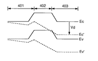
ここで、短チャネル効果が生じる場合におけるチャネル形成領域周辺のエネルギー状態を図4を用いて説明する。図4において実線で示す状態図はドレイン電圧が0Vの時のソース領域401、チャネル形成領域402、ドレイン領域403のエネルギーバンド図である。
【0014】
この状態において十分大きいドレイン電圧Vdが印加されると、図4において点線で示す様な状態へと変化する。即ち、ドレイン電圧Vdにより形成されたドレイン領域403の空乏層電荷や電界が、ソースおよびチャネル領域401、402の空乏層電荷に影響を与え、エネルギー(電位)状態はソース領域401からドレイン領域403にかけて連続的に変化する様になる。
【0015】
そして、このような短チャネル効果が半導体素子、例えばIG−FETに与える影響としてはしきい値電圧(Vth)の低下やパンチスルーによる素子耐圧の低下等の現象がよく知られている。また、パンチスルー現象によってドレイン電流に対するゲイト電圧の影響が低下するとサブスレッショルド特性が悪くなることも知られている。
【0016】
まず、しきい値電圧の低下はNチャネル型FETに対してもPチャネル型FETに対しても同様に見られる現象である。また、この低下の度合いはドレイン電圧に依存するばかりでなく、基板不純物濃度、ソース/ドレイン拡散層深さ、ゲイト酸化膜厚、基板バイアス等の様々なパラメータに依存する。
【0017】
しきい値電圧の低下は消費電力を小さくするといった意味では望ましいことであるが、一般的には集積回路の駆動電圧が小さくなることで周波数特性が高くならないといったデメリットが問題となってしまう。
【0018】
また、チャネル長が短くなるとドレイン側の空乏層がソース側の空乏層と繋がる状態を形成してソース近傍の拡散電位を下げるためチャネルが形成されていなくてもソース/ドレイン間に電流が流れる様になる。これがパンチスルーと呼ばれる現象である。
【0019】
パンチスルー現象が生じると飽和領域でもドレイン電流が飽和しなくなるためドレイン電圧の増加に伴って大電流が流れる様になり、ソース/ドレイン間の素子耐圧が大幅に低下することが問題となっていた。
【0020】
また、パンチスルー現象に伴うサブスレッショルド特性の劣化とはサブスレッショルド係数(S値)が大きくなる、即ちFETのスイッチング特性が劣化することを意味している。ここでサブスレッショルド特性に及ぼす短チャネル効果の影響を図5に示す。
【0021】
図5は横軸にゲイト電圧Vg、縦軸にドレイン電流Idの対数をとったグラフであり、501の領域における傾き(サブスレッショルド特性)の逆数がS値である。この図5ではチャネル長を徐々に短くした時の特性の変化を比較しており、矢印の方向に向かってチャネル長は短くなっている。
【0022】
その結果、チャネル長が短くなるに従って特性の傾きが小さくなる、即ちS値が大きくなる傾向にあることが確認できる。このことは、チャネル長が短くなるに従ってFETのスイッチング特性が劣化することを意味する。
【0023】
以上説明した様な短チャネル効果を抑制する手段として様々な技術が提案されてきている。例えば、埋め込み酸化膜で基板と素子とを絶縁するタイプのSOI構造(貼り合わせ技術やイオン注入技術を利用したもの等)では、埋め込み酸化膜の膜厚を薄くすることが短チャネル効果の抑制に効果的であることが報告されている。しかし、これだけでは十分な解決までには至らなかった。
【0024】
また、チャネル長が0.1 μm程度と極めて短いSOI構造の半導体装置は、チャネル領域における不純物元素の存在確率が極めて小さい(1個乃至数個)という特徴を有しており、室温でも電子の移動速度が通常よりも速くなる現象(速度オーバーシュート効果)が確認されている。(K.Ohuchi et al.,Jpn.J.Appl.Phys. 35, 960(1996). )。
【0025】
さらに、その効果を利用して高速動作性を向上させた高速半導体装置も発表されている。しかしながら、その様な高速半導体装置においては、前述の様な短チャネル効果によるパンチスルー現象とそれに伴う耐圧の劣化といった諸問題は解決されていないのが現状である。
【0026】
また、短チャネル効果によるしきい値電圧の低下を抑制するための手段としては、チャネル形成領域全体に均一に一導電性を付与する不純物元素を添加して、その添加量でもってしきい値電圧を制御する方法が採られてきた。しかし、この方法では添加した不純物がキャリアを散乱させる原因となるのでキャリアの移動度を低下させてしまうことが問題となっていた。
【0027】
また、SOI基板のマザーサブストレートとなる単結晶シリコン基板の作製方法には、極めて酸素含有量の低いFZ法と、応力緩和および反り防止のためにある程度の酸素を含有させたCZ法で形成されたものがある。通常、メモリICやロジックIC用にはCZ法による単結晶シリコン基板が用いられる。
【0028】
しかし、CZ法で形成された単結晶シリコン基板は酸素含有量が減少するに従って熱履歴などによる反り量が増加する特徴があり、逆に反り量を十分低減しうるレベルまで酸素含有量を上げる(通常、 1〜2 ×10¹⁸atoms/cm3 程度)と、酸素原子がキャリアの移動を妨げてしまう様なことが起こりうる。
【0029】
【発明が解決しようとする課題】
現状の半導体産業においては、極限まで集積化された半導体集積回路が求められており、個々の半導体素子の微細化をどこまで追求できるかが鍵となっている。しかし、ディープサブミクロン領域のファインパターンを形成する技術が開発されたとしても、前述の様な短チャネル効果の問題が素子の微細化を阻む致命的な障害となっていた。
【0030】
本発明は上記問題点を鑑みてなされたものであり、半導体素子の微細化に伴う短チャネル効果を効果的に抑制するための技術を開示するものである。そして、短チャネル効果によって実現が困難であったディープサブミクロン領域の微細素子を形成可能とすることを課題とする。
【0031】
【課題を解決するための手段】
本明細書で開示する発明の構成は、
絶縁性基板または絶縁層上に形成された結晶半導体を利用して形成されたソース領域、ドレイン領域およびチャネル形成領域と、
前記チャネル形成領域上に形成されたゲイト絶縁膜およびゲイト電極と、
を少なくとも有するSOI構造で構成される絶縁ゲイト型半導体装置であって、
前記チャネル形成領域はキャリアが移動する領域と、
前記ドレイン領域より前記チャネル形成領域およびソース領域に向かって広がる空乏層をピニングするために人為的かつ局部的に形成された不純物領域と、
を有し、
前記不純物領域にはエネルギーバンド幅(Eg)を広げる不純物元素が添加されていることを特徴とする。
【0032】
また、他の発明の構成は、
絶縁性基板または絶縁層上に形成された結晶半導体を利用して形成されたソース領域、ドレイン領域およびチャネル形成領域と、
前記チャネル形成領域上に形成されたゲイト絶縁膜およびゲイト電極と、
を少なくとも有するSOI構造で構成される絶縁ゲイト型半導体装置であって、
前記チャネル形成領域はキャリアが移動する領域と、
不純物元素の添加により所定のしきい値電圧に制御するために人為的かつ局部的に形成された不純物領域と、
を有し、
前記不純物領域にはエネルギーバンド幅(Eg)を広げる不純物元素が添加されていることを特徴とする。
【0033】
また、他の発明の構成は、
絶縁性基板または絶縁層上に結晶半導体を形成する工程と、
前記結晶半導体を利用してソース領域、ドレイン領域およびチャネル形成領域とを形成する工程と、
前記チャネル形成領域において人為的かつ局部的に不純物領域を形成する工程と、
前記チャネル形成領域上にゲイト絶縁膜およびゲイト電極とを形成する工程と、
を少なくとも有するSOI構造で構成される絶縁ゲイト型半導体装置の作製方法において、
前記チャネル形成領域はキャリアが移動する領域と前記不純物領域とで構成され、
前記不純物領域にはエネルギーバンド幅(Eg)を広げる不純物元素が人為的かつ局部的に添加されていることを特徴とする。
【0034】
本発明の主旨は、チャネル形成領域に対して人為的かつ局部的に形成した不純物領域により、ドレイン領域からチャネル形成領域に向かって広がる空乏層を効果的に抑制し、短チャネル効果によって引き起こされるパンチスルー現象、サブスレッショルド特性の劣化、耐圧の劣化などの諸問題を防止することにある。
【0035】
なお、本出願人はあたかもチャネル形成領域に不純物領域のピンを形成することに似ていることから、本発明によるデバイスをピニング型半導体装置と呼んでいる。なお、本明細書中において「ピニング」とは「抑止」を意味しており、「ピニングする」とは「抑止する」という意味で用いている。
【0036】
即ち、チャネル形成領域に対して局部的に不純物領域を形成し、その領域をエネルギー的な障壁として利用するものである。そして、不純物領域をエネルギー的な障壁として利用することでドレイン領域側の空乏層がチャネル形成領域側へ広がるのをエネルギー的に抑止し、それによってチャネル形成領域に形成される電界がゲイト電圧のみによって制御される様にする。
【0037】
本発明は上記構成をなすために不純物領域を形成する不純物元素としてエネルギーバンド幅(Eg)を広げる不純物元素を用いている。その様な不純物元素としては炭素(C)、窒素(N)、酸素(O)から選ばれた一種または複数種類の元素が挙げられる。
【0038】
この場合、添加された不純物はチャネル形成領域に局部的にエネルギーバンド幅の大きいエネルギー障壁を形成する。この様に炭素、窒素、酸素を用いた場合には、図6(A)で示す状態であったチャネル形成領域のエネルギーバンドを図6(B)で示す状態とし、エネルギーバンド幅(Eg)を広げることで障壁ΔE(拡散電位差またはビルトイン電位差と呼ばれる)が形成される。
【0039】
また、本発明において「キャリアが移動する領域」が真性または実質的に真性であることはSOI構造の半導体装置に特有の注目すべき特徴である。なお、本明細書において真性な領域とは、例えばサファイア基板上にエピタキシャル成長させた単結晶シリコン層の様な不純物元素を含有しない領域、またはN型やP型を付与する不純物元素および炭素、窒素、酸素といった不純物元素を意図的に添加しない領域を指している。
【0040】
また、実質的に真性とは、結晶半導体(本明細書では単結晶シリコンを代表例とする)中において、意図的にN型やP型を付与する不純物元素を添加しなくても生ずる導電型を相殺した領域、又はしきい値制御が可能な範囲においてソースおよびドレイン領域と同一導電型を呈する領域を指している。
【0041】
また、実質的に真性な領域において、結晶半導体(結晶シリコン)表面近傍における一導電性を付与する不純物元素(リンまたはボロン)の濃度は 5×10¹⁵atoms/cm3 以下(好ましくは 5×10¹⁴atoms/cm3 以下)であり、酸素濃度は 2×10¹⁸atoms/cm3 以下(好ましくは 1×10¹⁷atoms/cm3 以下)である。
【0042】
なお、ここで言う結晶半導体表面近傍とはデバイス素子として機能しうる領域を指しており、SOI基板の単結晶シリコン層、もしくは、少なくともキャリアが移動する領域(反転層)を含む領域を指す。また、本発明の特徴である不純物領域には不純物元素が大量に含まれていて当然であるので、上記不純物濃度の範囲に当てはまらないことは言うまでもない。
【0043】
また、本明細書中においては結晶半導体として単結晶シリコンを代表例とするが、この単結晶シリコンとは現在のIC、LSIレベルで一般的に用いられている水準の単結晶シリコンは勿論のこと、さらに高水準の単結晶シリコン(究極的には宇宙空間で作製された様な理想状態の単結晶シリコン)もその範疇に含まれるものとする。
【0044】
また、SOI構造は大別して2種類があり、一つはSOS基板に代表される様に絶縁性基板上に単結晶シリコン層を成長させた構造である。もう一つはSIMOX基板やウェーハ接合SOIに代表される様に単結晶シリコン基板中に絶縁層を形成させた構造である。特にSIMOX基板は1986年以降SOI構造の主要な形成技術となっている。
【0045】
本発明はSOI構造の作製方法に関係なく、SOI基板全般に活用することができる。即ち、半導体装置を作製する際に、どの様な方法でSOI基板を作製するか、もしくはどの様な方法で単結晶シリコン層を得るかは、作製者が適宜決定することができる。
【0046】
【発明の実施の形態】
ここでSIMOX基板上に形成された半導体装置に対して本発明を適用した場合について図1を用いて説明する。なお、説明はNチャネル型FETを例にとって行う。
【0047】
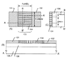
図1(A)に示すのは本発明のIG−FETのソース領域、ドレイン領域およびチャネル形成領域を上面から見た時の状態の模式図である。なお、101がソース領域、102がドレイン領域、103がチャネル形成領域である。
【0048】
そして、本発明の特徴はチャネル形成領域103内に人為的かつ局部的に不純物領域104が形成されている点である。ここでは不純物領域104を線状パターン形状に形成した場合を例とするが、不純物領域はドットパターン状に設けることも可能である。
【0049】
なお、不純物領域104をチャネル方向(ソース−ドレイン間を結ぶ方向またはキャリアが移動する方向)と概略平行な線状パターン形状に設けた場合、不純物領域が側壁となってキャリアの移動を規定するエネルギー的なレールを構成するため、キャリア同士の衝突による散乱の発生確率が低減されて移動度が向上するといった利点が生まれるので望ましい。
【0050】
また、本出願人はキャリアの移動するパス、即ち不純物領域と不純物領域との間の領域をポテンシャルスリット領域又はレーン領域と呼んでいる。
【0051】
ここではチャネル形成領域103内の一端から他端に向かって(例えば、ソース領域101からドレイン領域102に向かって)チャネル方向と概略平行に線状パターン形状を有する不純物領域104を形成した場合についての説明を行う。また、添加する不純物として酸素を用いた場合を例とする。
【0052】
添加された不純物(酸素)はチャネル形成領域103内に局部的にエネルギーバンド幅の大きいエネルギー障壁を形成する。図1の様に不純物元素として酸素を用いた場合には、前述の様に図6(A)で示す状態であったチャネル形成領域103のエネルギーバンドを図6(B)で示す状態とし、エネルギーバンド幅(Eg)を広げることで障壁ΔEを形成する。また、酸素を添加して形成された不純物領域は例えば SiOx で示される様な構造の絶縁性の高抵抗領域となり電気的にも障壁となる。
【0053】
特に、図1(A)に示す様にドレイン領域102とチャネル形成領域103との接合部は最も電界の変化の激しい領域であるので、この位置に不純物領域104がかかる様にしておくことが望ましい。また、ゲイト電極による電界がドレイン領域102内にもおよぶ場合はドレイン領域102内部に入り込む様に不純物領域104を形成すると良い。逆にソース領域101内部にはなるべく不純物領域104が入り込まない構成とすることが好ましい。
【0054】
また、この場合の様に不純物元素として酸素(他にも炭素、窒素等)を用いる場合においては、どの場合も不純物領域を絶縁性のエネルギー障壁として活用するのでNチャネル型TFTとPチャネル型TFTとで共通化することができる。このことは、本発明をCMOS回路に適用した場合に製造工程を簡略する上で有利であることを意味する。
【0055】
また、これらの不純物元素は、母体基板がシリコンである場合、シリコン原子と強く結合するので加熱処理などにより再拡散する恐れが少ない。
【0056】
また、本発明は 0.35 μm以下(特に、0.1 μm以下)、さらには0.01μm以下といったディープサブミクロン領域の微細加工を必要とする微細素子を形成する際に極めて効果的である。従って、チャネル形成領域の長さ(チャネル長またはソース/ドレイン間距離)も0.01〜0.35μmといった短いものとなるため、不純物領域はさらに細かいパターンを切らなければならない。
【0057】
例えば、線状パターン状の不純物領域を形成する際にレジストマスクを利用する場合にはレジストマスクに開孔を設けるパターニングは解像度の問題から通常の露光法を用いることができない。その様な場合においては、KrFやArF等のエキシマレーザーを用いた露光法、電子(ビーム)描画法、 FIB(Focussed Ion Beam )法等の技術を用いて行うことでディープサブミクロン領域の微細パターンを実現すれば良い。
【0058】
また、不純物領域はパターニングにより人為的に配列して形成されるので、図1(A)の様な配置だけでなく、任意の様々な配置とすることが可能である。
【0059】
次に、図1(A)に示すソース領域/チャネル形成領域/ドレイン領域の構成を有する絶縁ゲイト型半導体装置(IG−FET)を駆動させた際に、どの様にして短チャネル効果が抑制されるかを以下に説明する。
【0060】
まず、図1(A)をA−A’で切った断面図を図1(B)に示す。105はシリコン基板、106は埋め込み酸化膜である。不純物領域104はソース領域101とドレイン領域102とを繋ぐ様にして形成されているので、A−A’で切った断面では図1(B)の様に不純物領域104が現れる。
【0061】
また、図1(A)をB−B’で切った断面図を図1(C)に示す。図1(C)はチャネル方向と垂直にチャネル形成領域103を切断した断面を表していることになる。
【0062】
この時、ある不純物領域104の幅はwpi,nで表され、その不純物領域間の間隔(ポテンシャルスリット領域の幅)はwpa,mで表される。ここでn、mはチャネル形成領域103内において、wpi,nがn番目の不純物領域の幅であり、wpa,mがm番目のポテンシャルスリット領域(キャリアの移動するパス)であることを意味している。
【0063】
ここまでの説明は単に構造についての説明であったが、次にその効果についての説明を行う。ここで図2(A)に示すのは、本発明のIG−FETのチャネル形成領域のみに着目した模式図である。
【0064】
まず、図1(B)に示す様な構造を有する半導体装置に対してゲイト電圧、ドレイン電圧を印加した場合には、図2(A)に示す様な状態でソース側空乏層201、チャネル側空乏層202、ドレイン側空乏層203が形成される。即ち、ドレイン側空乏層203は不純物領域204が障壁となってソース側への広がりを防止された形となる。なお、205は埋め込み酸化膜の一部である。
【0065】
図1(B)では判りにくいが不純物領域204は図1(A)に示す様に配置されており、チャネル方向から見ると図1(C)の様な状態で配置されている。従って、チャネル形成領域103を塞ぐ格子状のフィルターでドレイン側空乏層の広がりを抑えているというモデルで考えれば理解しやすい。
【0066】
従って、本発明による構造の半導体装置においては、図2(A)に示す様に空乏層が実質的に相互に干渉することなく分断される。即ち、ソース側空乏層201、チャネル側空乏層202が、ドレイン側空乏層203の影響を受けないで分布することになるので、エネルギー状態は図2(B)に示す状態となる。
【0067】
即ち、図4に示した従来のエネルギー状態図と異なり、チャネル領域のエネルギー状態は殆どゲイト電圧による電界のみに制御されるので、チャネル領域に対して概略平行な形状を有する。従って、短チャネル効果特有のパンチスルー現象の様な問題がなく、ドレイン耐圧の高い半導体装置を作製することができる。
【0068】
さらに、図2(A)に示す様に、本発明においてはドレイン電圧が高くなった状態においても空乏層の占める体積が図3に示した様な従来のものと比べて減少しているため、従来よりも空乏層電荷が小さく、空乏層容量が小さい特徴がある。ここで、S値を導出する式は次式で表される。
【0069】
【数3】

即ち、前述の様に、図5に示すグラフにおいて501で示される領域における傾きの逆数を表していることが判る。また、数3の式は近似的に次式の様に表すことができる。
【0071】
【数4】
数4において、kはボルツマン定数、Tは絶対温度、qは電荷量、Cd は空乏層容量、Citは界面準位の等価容量、Coxはゲイト酸化膜容量である。従って、本発明によれば空乏層容量Cd が従来よりも十分小さくなるので、S値を85mV/decade 以下(好ましくは70mV/decade 以下)の小さな値とすることができる、即ち優れたサブスレッショルド特性を得ることができるのである。
【0073】
また、本発明が目指すところは、空乏層容量Cd および界面準位の等価容量Citを0に可能な限り近づけることである。即ち、Cd =Cit=0となる理想状態におけるS値(60mV/decade )に近づけることにある。
【0074】
また、チャネル形成領域が図1(C)に示す構造となっていることは短チャネル効果によるしきい値電圧の低下を緩和する上で非常に重要である。なぜならば、図1(C)に示す構造が意図的に狭チャネル効果を生み出すために必要な構成だからである。
【0075】
この狭チャネル効果とは、元来バルクシリコン上に形成したMOSFETで確認されている現象であり、チャネル幅が狭くなった時に素子を分離するフィールド酸化膜のバーズビークやチャネルストッパーの不純物拡散の影響等を受けてしきい値電圧が増加するという現象である。
【0076】
本発明の構成となる思想の一つは、チャネル形成領域に人為的に不純物領域を形成・配置することで意図的に狭チャネル効果を生じさせることである。そして、本発明の構成は不純物領域間の距離(図1(C)におけるwpa,mに相当する)を3 〜 300 nm( 好ましくは3 〜 100 nm) の範囲で精密に制御することでしきい値電圧の制御を行うという思想に基づいている。
【0077】
例えば、図1(C)に示す様にある断面に着目すると、チャネル形成領域の幅Wは不純物領域104によって分断され、実質的に狭いチャネル幅wpa,mを持つ複数のチャネル形成領域の集合体と見なすことができる。
【0078】
即ち、その複数の狭いチャネル幅wpa,mを有する領域において狭チャネル効果が得られると考えられる。マクロ的に見ると図1(A)に示す様にチャネル形成領域全体にこの様な狭チャネル効果が得られる領域が存在するので、全体的にも狭チャネル効果が得られ、しきい値電圧が増加すると考えられる。
【0079】
従って、チャネル長に短くなることで短チャネル効果によってしきい値電圧が低下したとしても、以上の理由により狭チャネル効果によってしきい値電圧を意図的に増加させてしきい値制御を行うことができるので、結果的にしきい値電圧の変化を緩和することが可能となる。
【0080】
以上の構成でなる本発明について、以下に記載する実施例でもって詳細な説明を行うこととする。また、これより記載する実施例は、本発明の構成の一例を示すものであり、半導体装置作製者の必要に応じて様々な応用を実施することが可能である。
【0081】
従って、特許請求の範囲に記載された事項は、以下に記載する実施例以外の応用であっても、本発明の構成をもってなしうる全ての発明をも包含するものと考える。
【0082】
【実施例】
〔実施例1〕
本発明を用いてSIMOX基板上に絶縁ゲイト型電界効果トランジスタを形成する例を図7を用いて説明する。なお、本実施例ではNチャネル型FETとPチャネルFETとを相補的に組み合わせたCMOS回路を形成する場合の例について説明する。
【0083】
まず、弱いN型またはP型導電性を有する単結晶シリコン基板701を用意する。そして、1×10¹⁸atoms/cm2 程度のドーズ量で酸素イオンを注入し、800〜1300℃の範囲内で加熱処理を行うことで埋め込み酸化膜702を形成する。こうして、厚さ0.05〜0.5 μmの埋め込み酸化膜702と厚さ10 〜 200 nm(好ましくは、20 〜 60 nm)の単結晶シリコン層703を得る。
【0084】
この際、SOI技術の最も大きな特徴の一つは、得られた単結晶シリコン層703に含まれる不純物元素(母体となる単結晶シリコン基板701に予め含まれてしまうもの)は1個乃至数個程度と殆ど皆無に等しく、極めて高純度の真性または実質的に真性な単結晶シリコン層が得られる点である。
【0085】
また、勿論埋め込み酸化膜702の膜厚や単結晶シリコン層703の膜厚は本実施例で示す範囲の値に限定されるものではなく、必要に応じて適宜調節することは可能である。SIMOX基板に関する詳細な説明は、例えば、丸善株式会社,志村史夫著,半導体シリコン結晶工学,平成5年9月30日発行,P217以下を参照すると良い。
【0086】
こうして図7(A)に示す様なSIMOX基板が得られる。勿論、SIMOX基板ではなく、ウェーハ貼り合わせ技術を用いて形成したSOI基板、サファイア基板の様な絶縁性基板上に単結晶シリコン層を成長させたSOS基板、多孔質シリコンの酸化を利用したFIPOS(Full Isolation by Porous Oxidized Silicon )基板等、他のタイプのSOI基板を用いても構わない。
【0087】
図7(A)の状態が得られたら、熱酸化処理を施すことにより図示しない薄い熱酸化膜を形成し、その上に窒化珪素膜でなるマスクパターン704、705を形成する。その際、マスクパターン704は後のNチャネル型FET上に、マスクパターン705は後のPチャネル型FET上に配置する。
【0088】
そして、その状態で1000〜1200℃程度の高温で熱酸化を行い、素子分離のためにフィールド酸化膜706を形成する。こうして、Nチャネル型FETの活性層となる領域707とPチャネル型FETの活性層となる領域708を得る。
【0089】
こうして図7(B)に示す状態が得られたら、マスクパターン704、705および図示しない熱酸化膜を除去する。そして、P(リン)を添加してNチャネル型FETのソース領域709、ドレイン領域710を形成し、さらにB(ボロン)を添加してPチャネル型FETのソース領域711、ドレイン領域712を形成する。
【0090】
この際、リンおよびボロンはレジストマスクを用いて打ち分ければ良い。また、この際に不純物を添加しない領域は真性または実質的に真性な領域であり、Nチャネル型FETのチャネル形成領域713、Pチャネル型FETのチャネル形成領域714を構成する。(図7(C))
【0091】
以上の様に、チャネル形成領域を真性または実質的に真性な領域とした場合、半導体装置の活性層は、Nチャネル型FETを例にすると、N+ (ソース領域)−I(チャネル形成領域)−N+ (ドレイン領域)の様な構成となる。ここで、N+ は強いN型を示すことを意味しており、Iは真性または実質的に真性であることを意味している。
【0092】
この様な構成の他にも、例えばN+ (ソース領域)−N--(チャネル形成領域)−N+ (ドレイン領域)、P+ (ソース領域)−P--(チャネル形成領域)−P+ (ドレイン領域)の様な構成を採ることも可能である。なお、N--は極弱いN型を、P--は極弱いP型を示すことを意味している。
【0093】
この様な構成は、移動度が向上する利点を有する反面、耐圧が低下する欠点が問題となっていた。しかしながら、本発明を利用することで高い耐圧特性を有する半導体装置を作製することが可能であるため、高い移動度と高い耐圧とを同時に満たすことができる。
【0094】
次に、図7(C)に示す状態が得られたら、図7(D)に示す様に、チャネル形成領域713、714に対して炭素(C)、窒素(N)、酸素(O)から選ばれた一種または複数種類の元素を添加し、空乏層のストッパーとなる不純物領域715、716を形成する。本実施例では不純物元素として酸素を用い、添加する領域715、716はパターニングにより図示しないレジストマスクに開孔を設けて選択的に設計する。
【0095】
なお、不純物領域715、716は極めて微細な加工寸法で形成する必要があるため精巧なリソグラフィ技術を必要とする。そのためには、電子ビームを用いる技術(電子描画法)、イオンビームを用いる技術(FIB 法) 、エキシマレーザーを用いる技術等を用いて線状パターン形状の露光を行えば良い。
【0096】
またこの時、ポテンシャルスリット領域の幅(wpa,m)は3 〜 300 nm( 好ましくは3 〜 100 nm) の範囲内に制御する。また、全ての間隔(wpa,m)は±20%以内(好ましくは±5 %以内)に納まる様に制御する。このポテンシャルスリット領域の幅(wpa,m)は狭チャネル効果に直接的に影響を与えるので精密に制御することが重要なのである。
【0097】
なお、ポテンシャルスリット領域の幅の下限界である3 nmという値は量子効果が起こらない限界値として定めている。本発明ではポテンシャルスリット領域の幅を量子効果の生じない又は現れない範囲内で制御する様に注意している。
【0098】
従って、図1(A)に示す上面図の様に配置された不純物領域715、716はポテンシャルスリット領域の幅(wpa,m)が全て揃った状態で形成される。そのため、しきい値電圧のバラツキ(狭チャネル効果のバラツキに起因する)や発熱のバラツキ(ポテンシャルスリット領域を流れる電流密度のバラツキに起因する)を効果的に抑制することができる。
【0099】
また、半導体装置の耐圧を効果的に向上させるためには図7(D)に示す様に不純物領域715、716をドレイン領域710、712に入り込む様に配置することが有効である。その際、ソース領域は入り込む様に配置してもしなくても良いが入り込まない方が好ましい(本実施例ではチャネル形成領域の境界を明確にするためソース領域にも不純物領域が入り込む場合を例とする)。
【0100】
また、チャネル形成領域とソース/ドレイン領域間にLDD領域を設ける構成とする場合には、LDD領域内部にまで、又はLDD領域を超えてドレイン領域内部にまで渡って不純物領域を形成することが好ましい。以上の様な構成は、半導体装置の耐圧をより向上させるために有効である。
【0101】
図7(D)に示す様な状態が得られたら、800 〜1200℃程度の温度範囲による熱酸化処理を行い10 〜 50 nmの熱酸化膜717、718を形成する。この熱酸化処理により形成された薄い熱酸化膜717、718はそのままゲイト絶縁膜として機能する。また、活性層/ゲイト絶縁膜界面は界面準位の少ない良好なものとなる。
【0102】
また、この熱酸化工程によって不純物領域715、716に添加された酸素がシリコンと反応して酸化絶縁物(酸化シリコン)に変成する。この状態では不純物領域715、716は共に、電気的に完全な絶縁領域となる。また、この酸化絶縁物中において、含有される酸素濃度の最大値は 1×10¹⁹〜 2×10²²atoms/cm3 の範囲となる。
【0103】
なお、上記熱酸化工程をハロゲン雰囲気で行うことも好ましい。その場合、不純物領域715、716とポテンシャルスリット領域との界面に偏析したNi(ニッケル)、Cu(銅)などの重金属をゲッタリング除去することができる。
【0104】
これら重金属は単結晶シリコンの形成過程等において内部に少なからず残留するものであり、キャリアの再結合中心となって移動度を低下させてしまう恐れがある。従って、熱酸化工程をハロゲン雰囲気で行えばハロゲン元素(例えば、塩素、弗素など)による金属元素のゲッタリング効果を期待することができる。
【0105】
さらに、チャネル形成領域713、714の上方において熱酸化膜717、718上にゲイト電極としてポリシリコン膜719、720を形成する。ゲイト電極719、720は成膜する段階で予め不純物元素を添加しておいて導電性を持たせれば良い。こうして図8(A)に示す状態が得られる。
【0106】
その後、図8(B)に示す様に、ゲイト電極719、720を覆う様にして窒化珪素膜を300 nmの厚さに成膜し、エッチバック法を用いてゲイト電極719、720の側面のみにサイドウォール721、722を残存させる。この際、ソース/ドレイン領域のゲイト絶縁膜は同時に除去される。
【0107】
次に、この状態で全面にスパッタ法により図示しないチタン膜を成膜し、加熱、レーザーアニール、ランプアニールなど手段のよるシリサイド形成を行う。この工程により、Nチャネル型FETのソース領域709およびドレイン領域710の表面ならびにゲイト電極719の表面にはチタンシリサイド723〜725が形成される。
【0108】
また、同時にPチャネル型FETのソース領域711およびドレイン領域712の表面ならびにゲイト電極720の表面にはチタンシリサイド726〜728が形成される。
【0109】
チタンシリサイド723〜728は極めて低抵抗であるので、後に形成する配線とのオーミック接触を確保する上で好ましい。(図8(B))
【0110】
シリサイド形成が終了したら、層間絶縁膜として窒化珪素膜729を成膜し、コンタクトホールを形成してNチャネル型FETのソース電極730、Pチャネル型FETのソース電極731およびN/Pチャネル型FET兼用のドレイン電極732を形成する。こうして図8(C)に示す様なCMOS構造のIG−FETが完成する。
【0111】
図8(C)に示す構造のCMOS回路は本発明のより短チャネル効果を問題としないで微細化することができるので、極めて集積度の高い集積化回路を構成することが可能である。
【0112】
また、本実施例ではシングルゲイト型のIG−FETを例としているが、SOI構造であるので活性層の上面および下面にチャネルを形成するダブルゲイト型FETを作製する場合にも本発明を適用できる。勿論、パワーMOSFET、MESFET、MISFET等に適用することもできる。
【0113】
また、本実施例ではIG−FETのチャネル形成領域に線状パターン状に不純物領域を形成することに特徴があるが、線状パターンの形成にはある範囲の条件を満たす必要がある。そのことについて、図9を用いて以下に記載する。
【0114】
図9において、901はチャネル形成領域の一部を示している。チャネル幅はWである。ここで、チャネル幅Wの内、線状パターン902が占有している幅をWpiと定義する。Wpiの値としては例えば1 〜 10 nmもあれば十分である。また、任意の線状パターン902の幅をWpi,1、Wpi,2、Wpi,3・・・Wpi,nとすると、Wpiは次式で表される。
【0115】
【数1】
但し、本発明の構成を達成するためにはチャネル形成領域の端部以外の領域に、不純物領域が少なくとも一つ形成されている必要があるのでnは1以上の整数である。
【0117】
また、チャネル幅Wの内、ポテンシャルスリット領域(キャリアの移動するパス)903が占有している幅をWpaと定義する。Wpaの値としては量子効果の現れないレベル、即ち3 〜 300 nm(好ましくは3 〜 100 nm)とする。本発明ではWpaをチャネル長(0.01〜0.35μm)の1/3 〜1/1 程度とすることでVth,nおよびVth,pを 0〜±0.3 Vの範囲に調節することができる。また、任意のポテンシャルスリット領域903をWpa,1、Wpa,2、Wpa,3・・・Wpa,mとすると、Wpaは次式で表される。
【0118】
【数2】
但し、前述の様にチャネル形成領域の端部以外の領域に不純物領域が少なくとも一つ形成されているので、チャネル形成領域は少なくとも2分されてmは2以上の整数となる。
【0120】
即ち、全チャネル幅WはW=Wpi+Wpa、かつ、n+mは3以上という関係が成り立っている。そして、WとWpi、WとWpaおよびWpiとWpaとの関係は、同時に以下の条件を満たすことが望ましい。
Wpi/W=0.1 〜0.9
Wpa/W=0.1 〜0.9
Wpi/Wpa=1/9 〜9
【0121】
これらの数式の意味するところは、Wpa/WまたはWpi/Wが0または1であってはならないという事である。例えば、Wpa/W=0(Wpi/W=1と同義)の場合、図9(B)に示す様にチャネル形成領域を完全に不純物領域で塞いでしまうので電流の流れるパスが存在しない状態となる。
【0122】
逆にWpa/W=1(Wpi/W=0と同義)の場合、図9(C)に示す様にチャネル形成領域に不純物領域が全く存在しないのでドレイン側空乏層の広がりを抑えることができない。
【0123】
以上の理由により、Wpa/WおよびWpi/Wの関係式は0.1 〜0.9 (好ましくは0.2 〜0.8 )の範囲に収まり、また、同時にWpi/Wpa=1/9 〜9 を満たすことが望ましい。
【0124】
また、本発明において線状パターン形状を有する不純物領域を図1(A)に示す様に配置することはFETの性能を示す代表的なパラメータである移動度の向上に対して非常に大きな意味がある。その理由について以下に説明する。
【0125】
移動度は半導体(本実施例ではシリコン基板)中のキャリアの散乱によって決まるが、シリコン基板における散乱は格子散乱と不純物散乱とに大別される。格子散乱はシリコン基板中の不純物濃度が低く、比較的高温で支配的であり、不純物散乱は不純物濃度が高く、比較的低温で支配的である。これらが影響し合って形成される全体的な移動度μは次式で表される。
【0126】
【数5】
この数5で示される式は、全体的な移動度μが、格子散乱の影響を受けた場合の移動度μl ( lはlattice を意味する) の逆数および不純物散乱の影響を受けた場合の移動度μi ( iはimpurityを意味する) の逆数の和に反比例することを意味している。
【0128】
ここで、格子散乱ではドリフト電界がそれほど強くなければ音響フォノンが重要な役割を果たし、その時の移動度μl は、次式の様に温度の-3/2乗に比例する。従って、キャリアの有効質量(m*)と温度(T)で決まってしまう。
【0129】
【数6】
また、不純物散乱による移動度μi は、次式の様に温度の3/2 乗に比例し、イオン化した不純物の濃度Ni に逆比例する。即ち、イオン化した不純物の濃度Ni を調節することで変化させることができる。
【0131】
【数7】
これらの式によると、従来の様にチャネル形成領域全体に不純物を添加するチャネルドープでは不純物散乱の影響を受けて移動度を稼ぐことができない。しかしながら、本発明では局部的に不純物領域を形成しているので、ポテンシャルスリット領域(Wpaの幅を持つ領域) には不純物が添加されない。
【0133】
即ち、理論的には数7においてイオン化した不純物の濃度Ni を限りなく0に近づけることを意味するため、移動度μi は限りなく無限大に近づいていくことになる。即ち、数5において1/μi の項を無視することができる程度にまで不純物を減少させることを意味するので全体の移動度μは限りなく移動度μl に近づいていく。
【0134】
また、キャリアの有効質量(m*)を小さくすることで移動度μl をさらに大きくすることも理論的には可能である。これは極低温の領域において、キャリア(特に電子の場合)の有効質量が結晶軸の軸方位に依存して変化する現象を利用することで成しうる。
【0135】
文献によれば、ソース/ドレイン間を結ぶチャネル方向(キャリアの移動する方向)が単結晶シリコンの<100>軸方向と一致する様に構成した時、最小の有効質量を得ることができる。
【0136】
例えば、図10に示す様に、(100)面を有する単結晶シリコン基板1001上にソース領域1002、チャネル形成領域1003、ドレイン領域1004が形成されているとする。この時、チャネル方向1005を[100]とした場合の様な時がこれに相当する。但し、この例は4°Kという極低温領域における結果である。
【0137】
また、結晶格子間をうまくキャリアがすり抜けて行ける様に、チャネル方向および不純物領域707の軸方向(配列方向)と、結晶格子の軸方向とを概略平行(軸方向のずれを±10°以内に収める)にさせることが望ましい。単結晶ならばシリコン原子は規則正しく配列しているので、結晶格子の配列方向と平行に移動するキャリアは格子散乱の影響を殆ど受けないで済む。
【0138】
例えば、単結晶シリコン基板において上記の様な方向における回転軸を0°とすると、他にも90°、180°、270°の回転軸の場合において同様の効果を得ることができる。
【0139】
以上の様に、チャネル形成領域を移動するキャリアはチャネル形成領域内に存在する不純物領域以外の領域を通る。この様子を図11の模式図を用いて簡単に説明する。
【0140】
図11(A)において、1101で示されるのはチャネル形成領域である。即ち、図11(A)はチャネル形成領域を右斜め上方から見た図である。本実施例を実施したチャネル形成領域は、立体的には図11(A)の様に不純物領域1102が形成されている。
【0141】
図11(A)に記載された矢印1103はキャリア(電子または正孔)の進行方向を示すものである。図11(A)に示す様にチャネル形成領域1101内には複数の不純物領域1102が配置されており、キャリアはそれら不純物領域1102以外の領域を通過する。
【0142】
キャリアの進行方向をチャネル形成領域1101の上面から見ると図11(B)の様に見える。図11(B)は図11(A)において、ACEFで表される面を見た図である。図11(B)に示される様に、キャリアは不純物領域1102を避け、不純物散乱のない領域を移動する。
【0143】
即ち、大部分のキャリアは矢印で示す様に、不純物領域1102の間を通ってソース/ドレイン間を移動する。勿論、不純物領域がドットパターン形状に設けられている様な場合には、不純物領域を避ける様にしてジグザグに移動する場合も含まれる。
【0144】
また、図11(C)に示すのは、チャネル形成領域1101を側面から見た図である。なお、図11(C)は図11(A)において、ABCDで表される面を見た図である。また、1103で示されるのは矢印であり、紙面に向かって手前方向に矢先が向いていることを示している。この図もキャリアが不純物領域1102の間を移動することを示している。
【0145】
また、線状パターン形状を有する不純物領域に挟まれた領域(ポテンシャルスリット領域)におけるエネルギー状態(電位状態)を模式的に表した分布図は図12(A)の様になっていると考えられる。
【0146】
図12(A)において、1201、1202で示される領域は不純物領域のエネルギー状態を示しており、エネルギー的に高い障壁となっている。そして、不純物領域から離れるに従って徐々にエネルギー的に低い領域1203となる。即ち、チャネル領域を移動するキャリア(ここでは電子を例にとる)は1203で示されるエネルギー状態の低い領域を優先的に移動し、1201、1202で示されるエネルギー障壁(不純物領域)は壁の様な役割を果たす。
【0147】
ここで、チャネル領域を移動するキャリア(電子)のイメージを模式的に図12(B)で表す。イメージ的には、チャネル領域を移動するキャリア1200は図12(B)に表す様にまるで雨樋の中を転がる球体の様にその方向性が規定され、ソース領域からドレイン領域に向かってほぼ最短距離を移動する。
【0148】
本出願人は図12(A)の様なエネルギー分布を電気的なスリットとして捉えてポテンシャルスリット領域と呼んでいる。また、図12(B)の様なモデルからレーンを転がる球体をイメージしてレーン領域とも呼ぶことがある。
【0149】
また、図12(B)に示す様に、チャネル形成領域には図12(A)に示した様なポテンシャルスリット領域が複数並列に配置されて構成されているが、1201、1202で示される領域を越えることがないため、隣接するポテンシャルスリット領域との間においてキャリアの移動は行われない。
【0150】
以上の理由によりキャリアが他のキャリアと衝突する確率は大幅に減少するため、移動度が大幅に向上する。即ち、本発明の構成は不純物散乱を低減するのみならず、キャリア同士の自己衝突による散乱をも低減することで大幅な移動度の向上を実現することができる。
【0151】
この様に従来においては常に悪影響を及ぼすとされてきたエネルギー障壁(グレインバンダリーなど)を逆に意図的に形成して利用するという本発明の発想は非常に新しいものである。
【0152】
〔実施例2〕
本発明において、チャネル形成領域に不純物領域を形成する手段として、不純物の偏析作用を利用した方法をとることもできる。本実施例では、その様な例として熱酸化膜近傍におけるボロン(B)およびリン(P)の偏析を利用した方法について図13を用いて説明する。
【0153】
実施例1に示した構造の半導体装置を作製する時、酸素を添加することによって不純物領域を形成した後に800 〜1200℃程度の加熱処理を行うと、添加された酸素とシリコン(Si)とが反応して熱酸化物が形成されることは述べた。
【0154】
本実施例はその際に不純物領域の周辺(ポテンシャルスリット領域)に含有されていた不純物元素(ボロンまたはリン)が不純物領域に偏析する現象を利用した技術である。ここで、熱酸化工程により熱酸化膜/シリコン界面近傍のボロンまたはリンの濃度がどの様な分布を示すかを図13を用いて説明する。
【0155】
図13に示す様に、Si中に存在する添加イオン(B、P)は酸化膜が形成されると再分布する。これは、シリコン(Si)中および熱酸化膜( SiOx )中において添加イオンの溶解度と拡散速度が異なるために起こる現象である。不純物のSi中における溶解度を [C] Siとし、 SiOx 中における溶解度を [C] SiOxとする時、平衡偏析係数mは次式で定義される。
m= [C] Si/ [C] SiOx
【0156】
この時、Si/SiOx 界面近傍の不純物の偏析はmの値に支配される。通常、Si中における不純物の拡散係数が十分大きいとして、m<1の場合、Si中の不純物は SiOx 中に取り込まれる(図13(A))。また、m>1の場合、SiO x が不純物を排斥し、その結果としてSi/SiOx 界面近傍の不純物濃度が増大する(図13(B))。
【0157】
文献値によると、ボロンのmの値は0.3 程度であり、リンのmの値は10程度である。従って、本実施例における熱酸化工程後のボロンの濃度分布は図13(A)の様になり、熱酸化膜中にボロンが取り込まれ、不純物領域の側面(Si/SiOx 界面近傍)におけるボロン濃度は極めて微量な状態となる。また、逆に形成された熱酸化物中には多量のボロンが含有される。
【0158】
この様な熱酸化膜中へのボロンの取込み現象は既に知られていたが、本発明の様にキャリアの移動する領域における不純物濃度を低減するためにこの現象を利用する発想は全く新しいものである。
【0159】
なお、図13(B)に示す様に、不純物元素としてリンを用いた場合には熱酸化膜とシリコンとの界面に偏析(パイルアップ)する。この現象もまた、リン濃度を低減する上で有効に利用することができる。
【0160】
以上の様に、本実施例の様な酸化物へのリンまたはボロンの偏析現象を利用することで大幅な移動度の向上を図ることが可能である。なぜならば、本実施例を実施すると不純物領域(代表的には SiOX で示される酸化物)周辺の不純物(リンまたはボロン)が不純物領域に収集されてしまうので、ポテンシャルスリット領域(キャリアが移動する領域)における不純物散乱の影響を極めて少なくすることができるからである。
【0161】
また、本実施例の技術にハロゲン元素による金属元素のゲッタリング効果を組み合わせることで、ポテンシャルスリット領域におけるキャリアの不純物散乱をさらに低減することも可能である。
【0162】
このことは、先にも述べた様に数5においてμi が大きくなることに相当するので、全体の移動度μは理想的にμ=μl に近づいていく。即ち、実質的に格子散乱のみで決まる極めて大きな移動度を実現しうることを示す。
【0163】
〔実施例3〕
本実施例では、チャネル形成領域に形成する不純物領域の形状をドットパターン状とする場合の例を示す。説明は図14を用いて行う。なお、説明の便宜上、図1と同じ符号を併用する。
【0164】
図14に示す半導体装置の構造は、図1において線状パターン形状を有する不純物領域をドットパターン形状に置き換えたものである。まず、図1と異なるのは図14(A)に示す様に不純物領域1401が配置される点である。
【0165】
また、図14(A)をA−A’で切断した断面は図14(B)に示す様になり、B−B’で切断した断面は図14(C)に示す様になる。
【0166】
なお、本実施例ではドットパターン状の不純物領域の例として円形の不純物領域を記載しているが、楕円形、正方形、長方形などであっても構わない。
【0167】
ドットパターン状に不純物領域を形成した場合、実施例1に示したレーン領域の様な役割はなくなるが、キャリアの移動しうる実効チャネル面積は増加するので半導体装置に流せる電流量を増やすことができる。
【0168】
〔実施例4〕
実施例1および実施例3では、不純物領域の形状として線状パターン形状の場合とドットパターン形状の場合とを最も単純な形状で説明した。本実施例では、不純物領域の形状の様々なバリエーションについて説明する。
【0169】
図15(A)に示す形状は線状パターン形状の他のバリエーションである。図15(A)に示す構造は、本発明においてドレイン領域側からチャネル形成領域側へと広がる空乏層をピニング(抑止)する効果をより確実にし、短チャネル効果に起因するパンチスルー現象を防止することを第一とした構造である。
【0170】
図15(A)において、不純物領域1501の特徴は、上面から見た場合に線状パターン形状の不純物領域の側面に対して凹凸部1502を付与した形となっており、いわゆるフィッシュボーン形状となっていることである。即ち、側面の凹凸部1502が空乏層の広がりを効果的に抑止するのである。
【0171】
また、図15(A)の構成をさらに発展させて、よりピニング効果を確実なものとした例が図15(B)に示す構成である。即ち、交互にかみ合ったフィッシュボーン形状とすることで空乏層に対する対向面積を増やし、空乏層の広がりを効果的に防止することができる。
【0172】
この際、図15(B)に示す様に、ある凹凸部(フィッシュボーンの骨に相当する部分)が、隣の不純物領域の凹凸部と交互に重なり合う様に形成することが望ましい(1503で示される領域)。
【0173】
ただし、この構造とした場合、キャリアが1504で示される破線の沿って移動するため移動距離が長くなることを避けられない。そして、移動距離が長くなるということは、その分キャリアの散乱確率が増加して移動度を低下させる要因となりかねない。
【0174】
しかし、本発明が効果を発揮する極めて微細な半導体装置においては、チャネル形成領域が真性または実質的に真性である以上、多少移動距離が長くなっても不純物散乱の影響は大きく変化しないと考えられる。それよりも微細化にともなう短チャネル効果(特にパンチスルー現象)の影響を抑制することの方が重要であると言える。
【0175】
また、ある一本の不純物領域に着目した場合、隣接する凹凸部同士の間の距離(図中、Lpaで表される距離)も制御が必要である。なぜならば、Lpaの長さがキャリアの移動度に影響してくるからである。
【0176】
即ち、ピニング効果を高めるためには距離Lpaを短くし、移動度向上に重きを置くなら距離Lpaを長くすることが好ましい。本発明では距離Lpaを7 〜 300 nm(好ましくは10 〜 100 nm)の範囲で制御する。
【0177】
また、本発明は線状パターンのみならず、ドットパターン状の不純物領域を形成する場合においても様々なバリエーションを採りうる。例えば、図15(C)に示す様に不純物領域1506が交互に配置された構成とすることができる。
【0178】
この場合、ドットパターン状の不純物領域1506間の隙間を隣接する列で補う構成となるので、空乏層の広がりを抑止する効果が強くなる。また、この場合もキャリアの移動経路は破線1507で示す様になるが、前述の様に素子が微細になればさほど問題とはならない。
【0179】
また、図15(D)に示す様に、ドットパターン形状の不純物領域1508をチャネル方向と垂直な楕円形または長方形とすることもできる。図15(D)に示す構成は空乏層の抑止を最重点課題とした時に有効な構成であると言える。
【0180】
以上の様に、短チャネル効果に起因するパンチスルー現象を効果的に防止するためには、不純物領域の形状を工夫すれば良い。不純物領域は人為的に形成されるので形状も作製者の自由に設計できる。
【0181】
特に、本実施例で示した様な図15(A)〜図15(D)に示した形状は、チャネル長が0.1 μm以下といった様な極めて微細な半導体装置を形成する場合に効果的である。なぜならば、その様な微細素子となるとパンチスルー現象による耐圧の低下が致命的な問題となるため、移動度の向上よりも耐圧の向上に重きを置くべきだからである。
【0182】
〔実施例5〕
本実施例では、本発明の不純物領域を形成する際に実施例4とは異なる工夫を施した例を示す。本実施例の説明は図16を用いて行なう。
【0183】
図16(A)に示すのは、不純物領域1601の幅(Wpi)をソース領域1602近傍とドレイン領域1603近傍とで変化させた例である。具体的には、ドレイン領域1603近傍に近づくに従い、徐々にWpiが増加していく様な構成とする。
【0184】
図16(A)の様な構成とすると、短チャネル効果に伴うパンチスルー現象の原因となるドレイン領域側の空乏層の広がりを効果的に抑制することができる。また、ソース領域側においてはポテンシャルスリット領域1604の幅(Wpa)が十分に広いのでキャリアの移動がスムーズに行なわれる。
【0185】
また、この構成は図16(A)の様な構成以外に限らず、例えば図16(B)の様にフィッシュボーン形状を有する不純物領域1605の凹凸部1606の長さを、ドレイン領域1607に近づくにつれて長くする様な構成としても達成することができる。
【0186】
また、図16(C)に示す様に、ドレイン領域1608近傍において不純物領域1609を構成する不純物元素の濃度を高くする構成とすることも可能である。この場合、図16(C)に示す様に、上面から見た場合にはソース領域1610からドレイン領域1608に渡って不純物領域1609が形成されている。
【0187】
そして、不純物領域1609を構成する不純物元素の濃度は、ソース領域1610近傍における濃度よりもドレイン領域1608近傍における濃度の方が高い構成とすることができる。(図16(D))
【0188】
なお、図16(D)は不純物領域1609内の不純物元素濃度の変化を表したグラフであり、横軸は距離、縦軸は濃度を表している。図16(D)に示した様に、ソース領域1611近傍の濃度プロファイルとドレイン領域1612近傍の濃度プロファイルを異なる様にするには、不純物領域1609を形成する際に添加する不純物元素の濃度を調節すれば良い。
【0189】
即ち、不純物元素の濃度プロファイルは図16(D)に示す様な形状にこだわる必要はなく、作製者の必要に応じて適宜不純物添加工程を調節して濃度プロファイルを決定すれば良い。
【0190】
以上の様に、本実施例に示した様な構成はソース領域およびドレイン領域の位置が特定されている場合において有効であり、例えば液晶表示装置の画素を駆動する半導体装置の様にソース/ドレインが充放電に応じて逆転する様な場合には必ずしも有効とは言えない。液晶表示装置に用いる場合には、周辺駆動回路を構成するインバータ回路などの様にソース/ドレインが特定される用途に用いるべきであると言える。
【0191】
また、本実施例では不純物領域の形状としてチャネル方向に概略平行な線状パターン形状を有する構成とする例を示したが、本実施例の構成をドットパターン形状に不純物領域に適用することは容易である。従って、本実施例は一例を示すのみであって、他の様々な考えうる例は作製者の必要に応じて適宜なされるものであると考える。
【0192】
〔実施例6〕
実施例1ではチャネル形成領域に対して人為的かつ局部的に不純物元素(炭素、窒素、酸素)を添加して不純物領域を形成する例を示した。本実施例では、不純物領域の形成方法として他の方法を用いた場合について図17を用いて説明する。
【0193】
図17(A)に示すのはSOI基板の単結晶シリコン層のみを拡大した図である。1701は絶縁層であり、1702が単結晶シリコン層である。SOI基板としては、SOS基板、SIMOX基板、FIPOS基板等を用いることができる。
【0194】
そして、電子ビーム法、FIB法、エキシマレーザー法などの微細リソグラフィ技術を利用して不純物領域を形成するためのレジストパターン1703をチャネル形成領域上に配置する。
【0195】
図17(A)に示す状態が得られたら、Ar(アルゴン)をイオン注入法により添加する。なお、本実施例ではArを用いるが、He(ヘリウム)、Ne(ネオン)等の希ガスを注入するのであっても良い。(図17(B))
【0196】
このイオン注入の目的は、単結晶シリコン層に対してダメージを与えることにあるため、電気的に不活性な元素を用いる。なぜならば、本実施例で開示する方法は、単結晶シリコンを熱酸化した際にダメージを受けた領域が優先的に酸化される性質を利用するものだからである。
【0197】
従って、図17(B)においてArが添加された領域1704は、他の領域に比べてダメージを受けた、結晶配列の乱れた領域となる。
【0198】
次に、レジストパターン1703を除去した後、図17(C)に示す様に、800 〜1200℃の温度範囲で加熱処理を行う。本実施例では、1000℃60min の処理の内、最初の30分を酸化性雰囲気で処理し、残りの時間を窒素(N2 )90%、酸素(O2 )9%、塩化水素(HCl)1%のハロゲン雰囲気に切り換えて処理を続ける構成とする。
【0199】
即ち、最初の30分間は熱酸化のための加熱処理であり、後の30分間はハロゲン元素による金属元素のゲッタリング効果を狙った加熱処理である。後者の加熱処理を窒素含有量の多い雰囲気で行うのは、単結晶シリコン層が過剰に酸化されるのを防止するためである。
【0200】
こうして図17(C)に示す様に、単結晶シリコン層には熱酸化膜1705が形成される。そして同時に領域1704が優先的に酸化反応が進行して、単結晶シリコン層内部まで侵入した不純物領域(この場合、酸化シリコンで成る)1706が形成される。なお、図17(C)では不純物領域1706が下方の絶縁層1701にまで達していないが、Arの注入条件によって絶縁層に達する様にする場合もあり得る。
【0201】
以上の様に、本実施例で開示する技術は、上記の様な過程で形成された不純物領域1706を空乏層をピニングする領域として活用するものである。また、本実施例は、例えば電子ビームや集束イオンビームを直接単結晶シリコン層に照射してダメージを与えても実施することができる。
【0202】
また、本実施例はハロゲン元素による金属元素のゲッタリング効果と、実施例2に示したリンやボロンの熱酸化膜への偏析現象を共に利用する構成になるので、真性または実質的に真性な、キャリアが移動する領域(特に、不純物領域1706の周辺)1707には、不純物散乱の原因や再結合中心となる不純物元素が存在しない。従って、極めて高い移動度を期待しうる半導体装置を作製することができる。
【0203】
〔実施例7〕
本発明の特徴はチャネル形成領域に対して人為的かつ局部的に不純物領域を設ける点にあるが、チャネル形成領域に局部的に添加された不純物元素(炭素、窒素、酸素から選ばれた一種または複数種類の元素)は、水素アニール処理を施した低酸素シリコン基板を用いる場合に有効な効果を示す。
【0204】
従来例で触れた様に、通常のLSI回路を構成する半導体装置(サイリスタを除く)はCZ法で形成されたシリコン基板を用いており、応力緩和のために所定量の酸素がシリコン基板中に含まれている。しかし、最近ではの酸化膜耐圧の向上、微小欠陥の低減の要求が強まり、水素雰囲気でのアニールによって表面層5μm位までの酸素濃度を 1×10¹⁷atoms/cm3 以下にまで下げた基板が多く用いられている。
【0205】
その反面、この様な低酸素処理を施したシリコン基板は基板表面層が応力に対して非常に脆くなってしまい、半導体装置の製造プロセスの過程でクラックや反りが発生する原因ともなってしまう可能性がある。
【0206】
しかしながら、本発明に低酸素処理を施したシリコン基板を用いるとチャネル形成領域に形成された不純物領域に応力が集中する様になるので、不純物領域が結晶半導体に発生する応力を緩和する緩衝領域としての機能を有する。
【0207】
この応力を緩和する緩衝領域として機能するという効果は、本発明における不純物領域の特筆すべき効果の一つである。なお、この効果は不純物元素として酸素を用いた場合において特に顕著である。
【0208】
従って、低酸素処理を施したシリコン基板を用いて半導体装置を作製する際に製造プロセス過程において発生する応力による影響を緩和することができるので、製造歩留りが大幅に向上する。
【0209】
また、この様なシリコン基板は酸化膜耐圧の向上、微小欠陥の低減の効果以外に、キャリアの不純物散乱の影響が低減するといった効果も期待できる。即ち、酸素を低減することはポテンシャルスリット領域をより真性または実質的に真性な領域に近づけることを意味しているので、キャリアの移動度を極めて高いものとしうる。
【0210】
〔実施例8〕
本実施例では、本発明を利用した半導体装置(半導体素子)で構成される集積化回路(本明細書では半導体装置の範疇に含まれる)について、いくつかの例を挙げて説明する。説明には図18および図19を用いる。
【0211】
図18(A)に示すのは、Nチャネル型FETとPチャネル型FETとを二階建てに積層して構成したスタックト型CMOS回路に本発明を適用した場合の例である。一般的には動作性能の問題からPチャネル型FETが下層側に形成されることが多い。本実施例も下層側をPチャネル型FETとしている。
【0212】
図18(A)において、下層は通常のIC技術で形成されたPチャネル型FETであり、1801はN型シリコン基板、1802はフィールド酸化膜、1803、1804はそれぞれソース領域およびドレイン領域である。本実施例では、低濃度不純物領域(ドレイン領域側はLDD領域と呼ばれる)1805、1806を設ける構成とする。
【0213】
また、1807は導電性を有するポリシリコンでなるゲイト電極であり、その直下には本発明の特徴である不純物領域1808が配置されている。なお、図18(A)では不純物領域1808の一端は低濃度不純物領域1806の内部にあり、他端はLDD領域1805を超えてドレイン領域1804の内部にある。
【0214】
上層にはSOI技術を用いてNチャネル型FETが形成されている。Nチャネル型FETの活性層となる単結晶シリコン層は公知のウェハーの貼り合わせ技術を利用することで得られる。従って、1809で示される層間絶縁膜は下層のFETを覆う層間絶縁膜と、接合するウェハーの熱酸膜との積層膜で構成され、接合面(点線で示される)を含んでいる。
【0215】
そして、公知のTFT技術を用いてソース領域1810、チャネル形成領域1811、ドレイン領域1812を形成する。ここでもチャネル形成領域1811を挟み込む様に低濃度不純物領域1813、1814が配置される。また、チャネル形成領域1811対しては本発明である不純物領域1815を配置する。
【0216】
さらに、ゲイト電極1816を覆って層間絶縁膜1817が成膜され、配線1818、1819、1820が形成される。なお、配線1818はPチャネル型FETのドレイン領域1804とNチャネル型FETのドレイン領域1812とに共通の配線となる。
【0217】
以上説明した構造でなる図18(A)に示すスタックト型CMOS回路は素子の占有面積を低減することができるため、VLSIやULSI回路を構成する際に集積度を向上させることができる。
【0218】
また、本発明を適用することで耐圧特性を損ねることなく高速動作性を追及することができるので、周波数特性の優れたCMOS回路を構成することが可能となる。
【0219】
次に、図18(B)に示すのは、CMOS回路とバイポーラトランジスタとを複合したBi−CMOS回路に本発明を適用した例である。ここでは、下層がバイポーラトランジスタであり、上層がSOI構造の半導体装置で構成されるCMOS回路である。
【0220】
図18(B)において、1821はP型シリコン基板であり、1822は埋め込みN+ 領域、1823はエピタキシャル成長により形成されたpウェルであり、埋め込みN+ 領域1822上のpウェルはN型にドーピングされてコレクタとして機能するnウェル1824となっている。また、1825は埋め込みN+ 領域1822からの取り出し電極となるDeepN+ 領域である。また、1826は通常の選択酸化法で形成されたフィールド酸化膜である。
【0221】
バイポーラトランジスタを構成するnウェル1824には活性ベースとなるp- 領域1827がまず形成され、次いで外部ベースとなるp+ 領域1828、エミッタ領域となるn+ 領域1829が配置される。
【0222】
以上の構成でなるバイポーラトランジスタの上方にはウェハー貼り合わせ技術を用いて得られた単結晶シリコン層を活性層とする、SOI構造のCMOS回路が構成されている。1830で示される層間絶縁膜が接合面(点線で示される)を含んでいる。ここでは、CMOS回路の詳細な説明は実施例1で十分に述べたのでここでは省略する。
【0223】
図18(B)では、Nチャネル型FETの不純物領域1831、Pチャネル型FETの不純物領域1832共に、ソース領域1833、1834には入り込まず、ドレイン領域1835、1836のみに入り込む様な配置とする。
【0224】
そして、上層のCMOS回路と下層のバイポーラトランジスタとを配線1837、1838で接続してBi−CMOS構造を実現することができる。
【0225】
この様にして構成されるBi−CMOS回路はバイポーラトランジスタの高速動作性とCMOS回路の低消費電力性を有効に併用するための回路構成である。また、本実施例の様に、CMOS回路とバイポーラトランジスタを積層化する三次元構造とすることで、従来の問題であった占有面積の大きさを大幅に小さくすることが可能である。
【0226】
次に、図19(A)に示すのは、SOI技術を用いて作製したDRAM(Dynamic Rondom Access Memory)に本発明を適用した例である。DRAMとは記憶する情報を電荷としてコンデンサに蓄える形式のメモリである。コンデンサへの情報としての電荷の出し入れは、コンデンサに直列に接続された半導体装置(電界効果トランジスタ)によって制御される。ここでは、スタックトキャパシタ型のDRAMについて説明する。
【0227】
図19(A)において、1901はシリコン基板、1902は、シリコン基板1901とその上に設けられる容量蓄積用電極1903とを分離する絶縁膜である。容量蓄積用電極1903の上方には高誘電率材料でなる絶縁膜1904を介して容量電極1905が設けられている。本実施例では絶縁膜1904としてTa2O5 を用いるが、他にもSi3N4 などを用いることができる。
【0228】
この様な構造によって、容量蓄積用電極1903と容量電極1905との間には大容量のキャパシタが形成される。図19(A)に示す積層構造において、下層は完全に容量を蓄積する領域として活用している点が特徴である。そして、その容量に蓄積する電荷の出し入れはSOI技術を用いて上層部に形成されたIG−FETによって成される。
【0229】
本実施例では上層に配置するデータ信号制御用に半導体装置として、LDD領域を設けたNチャネル型FETを用いている。活性層となる単結晶シリコン層はウェハー貼り合わせ技術を用いて得られるが、レーザー又は電子ビームによるポリシリコン(又はアモルファスシリコン)の再結晶化技術を用いても良い。なお、図中の点線で示されるのは貼り合わせの接合界面である。
【0230】
単結晶シリコン層でなる活性層はソース領域1906、ドレイン領域1907で構成され、チャネル形成領域には本発明の不純物領域1908が配置されている。なお、不純物領域1908はLDD領域1909を突き抜けてドレイン領域1907の内部にまで入り込む様にして設けられている。
【0231】
ビット線1910で送られてきたデータ信号は、ワード線1911の電圧を制御することでドレイン電極1912に伝えられる。そして、その信号は上層のドレイン電極1912と下層の容量電極1905とを接続する埋め込みプラグ1913を介して下層にキャパシタ(容量)に蓄積される。
【0232】
DRAMの特徴は1個のメモリを構成する素子数がIG−FETとキャパシタだけで非常に少ないので、高集積密度の大規模メモリを構成するのに適していることである。また、製造コストも低く抑えられるので、現在最も大量に使用されている回路であると言える。
【0233】
次に、本発明を利用して作製したFETをSRAM(Static Rondom Access Memory )に適用した例について説明する。説明には図19(B)を用いることとする。
【0234】
SRAMはフリップフロップ等の双安定回路を記憶素子に用いたメモリであって、双安定回路のON−OFFあるいはOFF−ONの2安定状態に対応して2進情報値(0または1)を記憶するものである。電源の供給がある限り記憶が保持される点で有利である。
【0235】
記憶回路はNMOS回路やCMOS回路で構成される。図19(B)に示すSRAMの回路はCMOS回路を組み合わせたセルの断面図である。なお、最下層に配置された2つのFETはどちらもPチャネル型FETであり、中層の2つのFETはどちらもNチャネル型FETである。従って、説明は基本的に図面に向かって右側の上下FETで構成されたCMOS回路を中心に説明する。
【0236】
図19(B)において、N型シリコン基板1914にはP型ウェルでなるソース領域1915ドレイン領域1916が形成され、ゲイト絶縁膜1917を介してゲイト電極1918が配置される。図面に向かって左右に配置される素子はフィールド酸化膜1919で分離されている。
【0237】
また、1920で示されるのは本発明の不純物領域である。ここではドレイン領域にのみ入り込む様な配置とし、ソース領域には不純物領域が入り込まない様に構成する。
【0238】
中層のNチャネル型FETの活性層はSOI技術の一つであるレーザー(又は電子)ビーム再結晶化法を用いて形成する。この技術は、平坦化された層間絶縁膜1921上にポリシリコン又はアモルファスシリコンを形成して、それをレーザービームや電子ビーム等で溶融させて再結晶化させるものである。
【0239】
勿論、ウェハー貼り合わせ技術等のSOI技術を用いても構わないのであるが、本実施例では再結晶化法を用いることで、中層のNチャネル型FETのドレイン領域1922を直接Pチャネル型FETのドレイン領域1916と接続する構成としている。
【0240】
上記手段によって得られた活性層(単結晶シリコン層)には公知のTFT技術を用いてソース領域1923ドレイン領域1922が設けられ、ゲイト絶縁膜1924を介してゲイト電極1925が配置されている。そのゲイト電極1925の直下(チャネル形成領域)には本発明の不純物領域1926がドレイン領域1922のみに入り込む様な構成で設けられている。
【0241】
Nチャネル型FETのゲイト電極1925は導電性を付与してポリシコンで形成されるが、ゲイト電極1925の形成と同時に同じ材料で接続配線1927を形成する。この接続配線1927は右側のCMOS回路の出力信号を、左側のCMOS回路のゲイト電極1928、1929へと伝えるための配線である。なお、図19(B)において、点線で示したのは図面上では記載されないが接続配線1927と各ゲイト電極1928、1929とが電気的に接続されていることを示している。
【0242】
そして、最上層にはトランスファゲートとして機能するNチャネル型FETが配置される。このFETの活性層はウェハー貼り合わせ技術を用いて得られた単結晶シリコン層である。単結晶シリコン層は島状に加工された後、ソース領域1930、ドレイン領域1931、本発明の不純物領域1932を形成されて活性層となる。
【0243】
このトランスファゲートとなるNチャネル型FETのドレイン領域1931は接続電極1933を介して中層に設けられた接続配線1927と電気的に接続されている。そして、ワード線1934に電圧を印加することでビット線1935からのデータ信号をCMOS回路へと伝達する。
【0244】
以上説明して様な構成でなるCMOS型SRAMは動作マージンが広い、データ保持電流が極めて少ないといった長所があり、低電圧のバッテリーバックアップ用に用いられることが多い。また、SRAMは、高速動作が可能で、信頼性が高くシステムへの組む込みが容易なことなどの特徴もある。
【0245】
以上の様に、本実施例で説明したBi−CMOS回路やSRAM回路等の半導体装置は、本発明を適用することで短チャネル効果を防止しつつ微細化することができるので、信頼性(高耐圧特性等)と高速動作特性を同時に追及することが可能となる。即ち、この先必要となるシステム・オン・チップ構想を念頭に置いた超高集積化回路を実現するために、本発明は絶大な効果を発揮する技術であると言える。
【0246】
〔実施例9〕
本実施例では、本発明を利用した半導体装置を製品(電子機器)に組み込んだ場合の一例を示す。ここでは、ノート型パソコンに組み込まれたIC回路を例にとって説明する。説明は図20を用いて行う。
【0247】
図20において、3001は本体、3002はフタ部、3003はキーボード、3004は画像表示部であり、本体3001内には様々な集積回路3005が組み込まれている。
【0248】
集積回路3005を取り出してみると、外部はパッケージ3011で覆われて内部の半導体チップは樹脂等で保護されている。また、内部の半導体チップはリード3012によって外部と接続される。通常、目にする集積回路(ICチップ)3005は、外目には黒色のパッケージ3011とリード3012しか見えないので完全にブラックボックスとなっている。
【0249】
そのパッケージ3011で保護された半導体チップを取り出して見ると、例えば次の様な構成となっている。まず、基板3013上には演算部(プロセッサー)3014とメモリ部3015が配置されている。なお、3016は半導体素子とリード3012とを接続するボンディング部である。
【0250】
演算部3014、メモリ部3015はCMOS回路、Bi−CMOS回路、DRAM回路、SRAM回路など、他にも様々な回路を用いて構成されている。本実施例で示した図20の様な構成は、同一基板上に演算部3014とメモリ部3015が配置されていることに特徴がある。これは、いわゆるシステム・オン・チップ(システムIC)と呼ばれる構想である。
【0251】
この様に演算部3014とメモリ部3015とが隣接した構成とすると、演算部3014とメモリ部3015との間のデータのやりとりが非常に高速で行われる様になるため、動作速度の速い回路を形成することが可能となる。
【0252】
また、ワンチップ上に必要な回路を全て集積化することも可能であるので、製造コストを大幅に低減することも期待できる。さらには、配置面積を減らすことで製品の小型化を図ることもできる。実施例8で説明した様に、SOI技術は三次元的な集積化回路を構成することができるので、今後、集積度は益々高密度となるに違いない。
【0253】
加えて、本発明を利用すれば短チャネル効果を問題とせずにIG−FET、さらには集積化回路の微細化を行うことができるので、上記の様なワンチップ化を実現することで半導体装置である応用電子機器のさらなる小型化、携帯化が期待できる。
【0254】
〔実施例10〕
本実施例では、本発明を適用したIG−FETおよびそれを組み合わせて構成される集積化回路を組み込んだ電子機器の例を示す。なお、前述の様に本明細書中では便宜上、IG−FET、集積化回路、電子機器等と記載しているが、基本的には全て半導体を利用して作製される装置であるので「半導体装置」の範疇に含まれているものとする。
【0255】
本発明を適用しうる半導体装置(電子機器)としては、一般的にIC回路を必要とする半導体装置全てが含まれる。従って、適用範囲は極めて広く日常の殆どの場面で使用される装置が含まれる。
【0256】
具体的には、例えば液晶表示装置、EL表示装置、CL表示装置といったアクティブタイプの電気光学装置およびTVカメラ、パーソナルコンピュータ、カーナビゲーション、TVプロジェクション、ビデオカメラ、携帯情報端末機器等が挙げられる。携帯情報端末機器としては、携帯電話やモバイル(モービル)コンピュータといった半導体装置が含まれる。以上に挙げた様な半導体装置として代表的な例を図21を用いて簡単に説明する。
【0257】
図21(A)はTVカメラであり、本体2001、カメラ部2002、表示装置2003、操作スイッチ2004で構成される。本発明は装置内部に組み込まれる集積化回路2005に適用することができる。
【0258】
図21(B)はカーナビゲーションであり、本体2101、表示装置2102、操作ボタン2103、アンテナ2104で構成される。本発明は装置内部に組み込まれる集積化回路2105に適用することができる。なお、表示装置2102はモニターとして利用されるが、地図の表示が主な目的なので解像度の許容範囲は比較的広いと言える。
【0259】
図21(C)は携帯情報端末機器(本実施例では携帯電話)であり、本体2301、音声出力部2302、音声入力部2303、表示装置2304、操作ボタン2305、アンテナ2306で構成される。本発明は装置内部に組み込まれる集積化回路2307に適用することができる。
【0260】
図21(C)に示す様な携帯電話は高周波動作を必要とする半導体装置であるので、極めて高速な動作特性を要求される。そこで本発明を適用することで耐圧を損ねることなく高速動作する集積化回路を組み込むことができる。
【0261】
図21(D)はビデオカメラであり、本体2401、表示装置2402、接眼部2403、操作ボタン2404、テープホルダー2405で構成される。本発明は装置内部に組み込まれる集積化回路2406に適用することができる。表示装置2402に映し出された撮影画像は接眼部2403を通してリアルタイムに見ることができるので、使用者は画像を見ながらの撮影が可能となる。
【0262】
以上の様に、本発明の応用範囲は極めて広く、半導体集積化回路を有する様々な半導体装置(電子機器を含む)に対して適用することが可能である。
【0263】
〔実施例11〕
本発明による半導体装置の電気特性は非常に優れたものであり、これを用いて構成した集積化回路は高い周波数特性を実現しうる。本実施例では、本発明を利用した半導体装置の性能に関する例を示す。
【0264】
本発明を利用して形成された半導体素子単体のデバイス特性(IG−FETの電流−電圧特性)は非常に優れたものとなり、Nチャネル型FETのしきい値電圧Vth,nは-0.3〜3.0 V、Pチャネル型FETのしきい値電圧Vth,pは-3.0〜0.3 Vの範囲(代表的には 0〜±0.3 Vの範囲)で必要とする駆動電圧に合わせて調節できる。また、S値は60〜85mV/decade 、ともすれば60〜70mV/decade の極めて優れたサブスレッショルド特性が得られる。
【0265】
また、実施例1で説明した様な理由により高い移動度(1000cm2/Vs以上)を得ることができる。移動度を計算式で求める場合、移動度はチャネル幅Wに反比例するので注意が必要である。本発明を実施する場合、チャネル形成領域においては不純物領域によって少なからずチャネル幅が狭くなっているので、実測チャネル幅Wpaを代入しなければ実際の移動度は得られない。
【0266】
以上の様な優れた電気特性を達しうる本発明の半導体装置で集積化回路を構成すると、極めて良好な周波数特性を得ることができる。例えば、本発明の半導体装置を用いて9段のリングオシレータを構成すると、3.3 Vの駆動電圧で2〜10GHzの周波数特性を実現しうる。
【0267】
また、例えば、高周波電子機器である携帯電話などの様に高い周波数特性を必要とする電子機器に対しても本発明は有効である。携帯電話の入力部等に用いられる集積化回路は、I/O 回路やMUX/DMUX回路等に様に2GHz程度(2.4 GHz)の周波数特性を必要とするのであるが、本発明はその様な高周波集積化回路に対しても十分に対応することができる。
【0268】
また、本発明をSOI構造の半導体装置に適用しているので、従来のバルクシリコン基板に作製した集積化回路よりも、10%以上も速い動作特性を有し、70%以下の消費電力で駆動しうる集積化回路を構成できる。
【0269】
【発明の効果】
本発明を利用することでチャネル長が短くなった場合に生じる短チャネル効果を防止することが可能となる。具体的には、まずドレイン側空乏層がソース領域やチャネル形成領域下に広がるのを、チャネル形成領域に局部的に形成した不純物領域で遮り、チャネル形成領域のエネルギー(電位)状態にドレイン電圧が影響しない構成とする。これによりパンチスルー現象やサブスレッショルド特性の劣化を防止することが可能となる。また、同時に高いドレイン耐圧を実現することができる。
【0270】
また、短チャネル効果の特徴の一つであるしきい値電圧の低下を狭チャネル効果によるしきい値電圧の増加によって抑制することができる。この狭チャネル効果は、チャネル形成領域に局部的に不純物領域を形成するという本発明の構成によって人為的に成しうる効果である。
【0271】
以上の様に、本発明を利用することでチャネル長の極めて短いディープサブミクロン領域における半導体装置においても、短チャネル効果を引き起こすことなく動作させることができる。従って、本発明の半導体装置を利用することで非常に高密度に集積化された集積化回路を構成することができる。
【0272】
また、本発明ではチャネル形成領域にエネルギー的にスリット状のレーン領域を形成することでキャリアの移動方向を規定し、キャリア同士の自己衝突による散乱を低減することが可能である。
【0273】
即ち、キャリアの移動度低下を招く原因となる不純物散乱、格子散乱、キャリア同士の自己衝突による散乱が大幅に低減され、移動度が大きく向上する。即ち、IG−FETに代表される半導体装置のより一層の性能向上が望める。
【図面の簡単な説明】
【図1】 チャネル形成領域の構成を示す図。
【図2】 チャネル形成領域の構成を示す図。
【図3】 従来の半導体装置を説明するための図。
【図4】 チャネル形成領域のエネルギー状態を示す図。
【図5】 従来の半導体装置の特性を説明するための図。
【図6】 チャネル形成領域のエネルギー状態を示す図。
【図7】 絶縁ゲイト型電界効果トランジスの作製工程を示す図。
【図8】 絶縁ゲイト型電界効果トランジスの作製工程を示す図。
【図9】 不純物領域の形状および配置を説明するための図。
【図10】 チャネル形成領域の構成を示す図。
【図11】 チャネル形成領域の構成を示す図。
【図12】 チャネル形成領域のエネルギー状態を示す図。
【図13】 不純物の偏析状態を説明するための図。
【図14】 チャネル形成領域の構成を示す図。
【図15】 チャネル形成領域の構成を示す図。
【図16】 チャネル形成領域の構成を示す図。
【図17】 不純物領域の作製工程を示す図。
【図18】 半導体装置の構成を示す図。
【図19】 半導体装置の構成を示す図。
【図20】 半導体装置の構成を示す図。
【図21】 半導体装置の構成を示す図。
【符号の説明】
101 ソース領域
102 ドレイン領域
103 チャネル形成領域
104 不純物領域
105 シリコン基板
106 埋め込み酸化膜[0001]
[Technical field to which the invention belongs]
The invention disclosed in this specification includes an insulating gate type semiconductor device having an SOI (Silicon-On-Insulator) structure, in particular, an insulating gate type field effect transistor (hereinafter simply referred to as IG-FET) and a manufacturing method thereof. About. Examples of the insulated gate semiconductor device having an SOI structure include a semiconductor device formed on an SOS (Silicon-On-Sapphire) substrate, a SIMOX (Separation-by-Implanted Oxygen) substrate, and the like.
[0002]
In particular, this technique is effective when a fine element having a channel length of 0.35 μm or less (particularly 0.1 μm or less) is manufactured. Therefore, the present invention can be applied to various semiconductor integrated circuits such as IC, VLSI, and ULSI configured by integrating IG-FETs.
[0003]
In this specification, the term “semiconductor device” means “a device that utilizes a semiconductor”, and not only a semiconductor element such as an IG-FET, but also an integration of a semiconductor element. The integrated circuit, and even electronic equipment incorporating the integrated circuit are included in the category of “semiconductor device”. Note that in this specification, for convenience of explanation, terms such as a semiconductor element, an integrated circuit, and an electronic device are properly used as necessary.
[0004]
[Prior art]
In recent years, integrated circuits such as VLSI have been increasingly miniaturized, and processing dimensions in the deep sub-micron region such as wiring widths of 0.35 to 0.1 μm or less and further 0.01 μm or less have been required. It is coming.
[0005]
At the same time, low power consumption is required, and the low power consumption characteristics of CMOS ICs are becoming indispensable configurations. When such a CMOS IC is miniaturized, a latch-up phenomenon that occurs between an N-type FET and a P-type FET becomes a problem, but an SOI-structured IG-FET solves this problem.
[0006]
Further, since the substrate and the element are completely insulated, the parasitic capacitance generated there can be greatly reduced, and high-speed operability can be pursued.
[0007]
As described above, a semiconductor device having an SOI structure is attracting a great deal of attention as a next-generation high-speed element, and is expected to increase in demand in the future.
[0008]
Such miniaturization of semiconductor elements has been advanced in accordance with a scaling law, and it has been generally known that miniaturization leads to improved characteristics of integrated circuits. However, when microfabrication is performed in the sub-micron region, a problem that simply does not follow the scaling law occurs.
[0009]
As such a problem, a phenomenon called a short channel effect is typically known. The short channel effect means that as the line width of the gate electrode becomes shorter, that is, as the channel formation region becomes shorter, the charge of the channel formation region is not limited to the gate voltage but also the depletion layer charge of the source / drain region, the electric field and the potential distribution. It is a phenomenon that is caused to become greatly affected.
[0010]
This state is simplified and shown in FIG. FIG. 3 shows a conventional semiconductor device formed on a SIMOX substrate, in which 301 is a silicon substrate and 302 is a buried oxide film layer formed by oxygen implantation. A crystalline semiconductor (single crystal silicon layer) is disposed on the buried
[0011]
Usually, the current flowing through the
[0012]
However, when the drain voltage Vd increases, the depletion layer in the vicinity of the
[0013]
Here, the energy state around the channel formation region when the short channel effect occurs will be described with reference to FIG. 4 is an energy band diagram of the
[0014]
When a sufficiently large drain voltage Vd is applied in this state, the state changes to a state shown by a dotted line in FIG. That is, the depletion layer charge or electric field of the
[0015]
As the influence of such a short channel effect on a semiconductor element, for example, an IG-FET, phenomena such as a decrease in threshold voltage (Vth) and a decrease in device breakdown voltage due to punch-through are well known. It is also known that when the influence of the gate voltage on the drain current is reduced due to the punch-through phenomenon, the subthreshold characteristic is deteriorated.
[0016]
First, the decrease in threshold voltage is a phenomenon that can be seen in the same way for both N-channel and P-channel FETs. The degree of this reduction depends not only on the drain voltage but also on various parameters such as substrate impurity concentration, source / drain diffusion layer depth, gate oxide thickness, and substrate bias.
[0017]
Although lowering the threshold voltage is desirable in terms of reducing power consumption, generally, there is a problem in that frequency characteristics do not increase due to a decrease in driving voltage of an integrated circuit.
[0018]
Further, when the channel length is shortened, a state where the drain side depletion layer is connected to the source side depletion layer is formed to lower the diffusion potential in the vicinity of the source, so that a current flows between the source and drain even if the channel is not formed. become. This is a phenomenon called punch-through.
[0019]
When the punch-through phenomenon occurs, the drain current does not saturate even in the saturation region, so that a large current flows as the drain voltage increases, and the device breakdown voltage between the source and drain is greatly reduced. .
[0020]
Further, the deterioration of the subthreshold characteristic due to the punch-through phenomenon means that the subthreshold coefficient (S value) is increased, that is, the switching characteristic of the FET is deteriorated. Here, the influence of the short channel effect on the subthreshold characteristic is shown in FIG.
[0021]
FIG. 5 is a graph in which the horizontal axis represents the gate voltage Vg and the vertical axis represents the logarithm of the drain current Id.5The reciprocal of the slope (subthreshold characteristic) in the 01 region is the S value. FIG. 5 compares changes in characteristics when the channel length is gradually shortened, and the channel length decreases in the direction of the arrow.
[0022]
As a result, it can be confirmed that the slope of the characteristic decreases as the channel length decreases, that is, the S value tends to increase. This means that the switching characteristics of the FET deteriorate as the channel length becomes shorter.
[0023]
Various techniques have been proposed as means for suppressing the short channel effect as described above. For example, in a SOI structure in which a substrate and an element are insulated with a buried oxide film (such as those using bonding technology or ion implantation technology), reducing the thickness of the buried oxide film can suppress the short channel effect. It has been reported to be effective. However, this alone did not reach a sufficient resolution.
[0024]
In addition, an SOI structure semiconductor device with an extremely short channel length of about 0.1 μm has a characteristic that the existence probability of an impurity element in the channel region is extremely small (one to several), and the electron transfer speed even at room temperature. Has been confirmed to be faster than usual (speed overshoot effect). (K. Ohuchi et al., Jpn. J. Appl. Phys. 35, 960 (1996)).
[0025]
Furthermore, a high-speed semiconductor device that has improved its high-speed operability by utilizing the effect has been announced. However, in such a high-speed semiconductor device, various problems such as the punch-through phenomenon due to the short channel effect and the accompanying breakdown voltage degradation have not been solved.
[0026]
In addition, as a means for suppressing a decrease in threshold voltage due to the short channel effect, an impurity element that uniformly imparts one conductivity is added to the entire channel formation region, and the threshold voltage is determined by the addition amount. The method of controlling has been taken. However, in this method, since the added impurity causes the carrier to be scattered, there is a problem that the mobility of the carrier is lowered.
[0027]
In addition, as a method for manufacturing a single crystal silicon substrate which becomes a mother substrate of an SOI substrate, an FZ method having an extremely low oxygen content and a CZ method containing a certain amount of oxygen for stress relaxation and warpage prevention are formed. There is something. Usually, a single crystal silicon substrate by a CZ method is used for a memory IC or a logic IC.
[0028]
However, the single crystal silicon substrate formed by the CZ method has a feature that the warpage amount due to thermal history increases as the oxygen content decreases, and conversely, the oxygen content is increased to a level at which the warpage amount can be sufficiently reduced ( Usually 1-2 × 10¹⁸atoms / cmThree Degree), oxygen atoms may interfere with carrier movement.
[0029]
[Problems to be solved by the invention]
In the current semiconductor industry, semiconductor integrated circuits integrated to the limit are required, and the key is how far down to the miniaturization of individual semiconductor elements can be pursued. However, even if a technique for forming a fine pattern in the deep sub-micron region has been developed, the problem of the short channel effect as described above has been a fatal obstacle that prevents miniaturization of the element.
[0030]
The present invention has been made in view of the above problems, and discloses a technique for effectively suppressing the short channel effect accompanying the miniaturization of a semiconductor element. It is another object of the present invention to make it possible to form a fine element in a deep submicron region that has been difficult to realize due to the short channel effect.
[0031]
[Means for Solving the Problems]
The configuration of the invention disclosed in this specification is as follows.
A source region, a drain region and a channel formation region formed using a crystalline semiconductor formed on an insulating substrate or an insulating layer;
A gate insulating film and a gate electrode formed on the channel formation region;
An insulated gate semiconductor device having an SOI structure having at least
The channel formation region is a region where carriers move,
An impurity region formed artificially and locally to pin a depletion layer extending from the drain region toward the channel formation region and the source region;
Have
An impurity element that broadens an energy band width (Eg) is added to the impurity region.
[0032]
In addition, the configuration of other inventions is as follows:
A source region, a drain region and a channel formation region formed using a crystalline semiconductor formed on an insulating substrate or an insulating layer;
A gate insulating film and a gate electrode formed on the channel formation region;
An insulated gate semiconductor device having an SOI structure having at least
The channel formation region is a region where carriers move,
An artificially and locally formed impurity region for controlling to a predetermined threshold voltage by addition of an impurity element;
Have
An impurity element that broadens an energy band width (Eg) is added to the impurity region.
[0033]
In addition, the configuration of other inventions is as follows:
Forming a crystalline semiconductor on an insulating substrate or insulating layer;
Forming a source region, a drain region, and a channel formation region using the crystalline semiconductor;
Artificially and locally forming an impurity region in the channel formation region;
Forming a gate insulating film and a gate electrode on the channel formation region;
In a method for manufacturing an insulated gate semiconductor device including an SOI structure having at least
The channel formation region includes a region where carriers move and the impurity region,
An impurity element that broadens an energy bandwidth (Eg) is artificially and locally added to the impurity region.
[0034]
The gist of the present invention is that the impurity region formed artificially and locally with respect to the channel formation region effectively suppresses the depletion layer extending from the drain region toward the channel formation region, and punch caused by the short channel effect. The purpose is to prevent various problems such as the through phenomenon, the deterioration of the subthreshold characteristic, and the deterioration of the breakdown voltage.
[0035]
The present applicant refers to the device according to the present invention as a pinning type semiconductor device because it is similar to forming a pin of an impurity region in a channel formation region. In the present specification, “pinning” means “suppression”, and “pinning” is used to mean “suppression”.
[0036]
That is, an impurity region is locally formed with respect to the channel formation region, and the region is used as an energy barrier. Then, by using the impurity region as an energy barrier, the depletion layer on the drain region side is energetically inhibited from spreading toward the channel formation region, and the electric field formed in the channel formation region is thereby only caused by the gate voltage. Be controlled.
[0037]
In the present invention, an impurity element that widens an energy bandwidth (Eg) is used as an impurity element that forms an impurity region in order to achieve the above structure. Examples of such an impurity element include one or more elements selected from carbon (C), nitrogen (N), and oxygen (O).
[0038]
In this case, the added impurity locally forms an energy barrier having a large energy bandwidth in the channel formation region. When carbon, nitrogen, and oxygen are used in this way, the energy band of the channel formation region that was in the state shown in FIG. 6A is changed to the state shown in FIG. 6B, and the energy band width (Eg) is By expanding, a barrier ΔE (called a diffusion potential difference or a built-in potential difference) is formed.
[0039]
Further, in the present invention, the “region in which the carrier moves” is intrinsic or substantially intrinsic, which is a remarkable feature peculiar to a semiconductor device having an SOI structure. Note that an intrinsic region in this specification refers to a region not containing an impurity element, such as a single crystal silicon layer epitaxially grown on a sapphire substrate, or an impurity element imparting N-type or P-type and carbon, nitrogen, This refers to a region where an impurity element such as oxygen is not intentionally added.
[0040]
In addition, substantially intrinsic means a conductivity type that occurs without the intentional addition of an impurity element imparting N-type or P-type in a crystalline semiconductor (in this specification, single crystal silicon is a typical example). Or a region exhibiting the same conductivity type as the source and drain regions in a range where threshold control is possible.
[0041]
In a substantially intrinsic region, the concentration of an impurity element (phosphorus or boron) imparting one conductivity in the vicinity of the surface of the crystalline semiconductor (crystalline silicon) is 5 × 10¹⁵atoms / cmThree Below (preferably 5 × 10¹⁴atoms / cmThree And the oxygen concentration is 2 × 10¹⁸atoms / cmThree Below (preferably 1 × 10¹⁷atoms / cmThree The following).
[0042]
Note that the vicinity of the surface of the crystalline semiconductor here refers to a region which can function as a device element, and refers to a single crystal silicon layer of an SOI substrate or a region including at least a region where carriers move (inversion layer). Needless to say, the impurity region, which is a feature of the present invention, does not fall within the impurity concentration range because a large amount of impurity elements is contained in the impurity region.
[0043]
In this specification, single crystal silicon is a typical example of a crystalline semiconductor, but this single crystal silicon is of course the level of single crystal silicon generally used at the current IC and LSI levels. Furthermore, higher-level single crystal silicon (which is ultimately single crystal silicon in an ideal state as produced in outer space) is also included in the category.
[0044]
There are roughly two types of SOI structures. One is a structure in which a single crystal silicon layer is grown on an insulating substrate as represented by an SOS substrate. The other is a structure in which an insulating layer is formed in a single crystal silicon substrate as represented by a SIMOX substrate or a wafer bonding SOI. In particular, since 1986, the SIMOX substrate has been the main technology for forming the SOI structure.
[0045]
The present invention can be applied to all SOI substrates regardless of the method for manufacturing the SOI structure. That is, when a semiconductor device is manufactured, a method for manufacturing an SOI substrate or a method for obtaining a single crystal silicon layer can be determined as appropriate by a manufacturer.
[0046]
DETAILED DESCRIPTION OF THE INVENTION
A case where the present invention is applied to a semiconductor device formed on a SIMOX substrate will be described with reference to FIG. The description will be given by taking an N-channel FET as an example.
[0047]
FIG. 1A is a schematic diagram of the state when the source region, drain region, and channel formation region of the IG-FET of the present invention are viewed from above. Note that 101 is a source region, 102 is a drain region, and 103 is a channel formation region.
[0048]
A feature of the present invention is that the
[0049]
Note that in the case where the
[0050]
Further, the applicant of the present application calls a path in which carriers move, that is, a region between the impurity region and the impurity region, as a potential slit region or a lane region.
[0051]
Here, the case where the
[0052]
The added impurity (oxygen) locally forms an energy barrier having a large energy bandwidth in the
[0053]
In particular, as shown in FIG. 1A, the junction between the
[0054]
Also, in this case, when oxygen (in addition to carbon, nitrogen, etc.) is used as the impurity element, the impurity region is utilized as an insulating energy barrier in any case, so that an N-channel TFT and a P-channel TFT are used. And can be shared. This means that the present invention is advantageous in simplifying the manufacturing process when applied to a CMOS circuit.
[0055]
In addition, when the base substrate is silicon, these impurity elements are strongly bonded to silicon atoms and thus are less likely to be re-diffused by heat treatment or the like.
[0056]
In addition, the present invention is extremely effective in forming a fine element that requires fine processing in the deep submicron region, such as 0.35 μm or less (particularly 0.1 μm or less), or 0.01 μm or less. Therefore, since the length of the channel formation region (channel length or source / drain distance) is as short as 0.01 to 0.35 μm, the impurity region must be cut into a finer pattern.
[0057]
For example, when a resist mask is used when forming a linear pattern-like impurity region, patterning for providing an opening in the resist mask cannot use a normal exposure method due to resolution problems. In such a case, a fine pattern in the deep submicron region can be obtained by using techniques such as an exposure method using an excimer laser such as KrF or ArF, an electron (beam) drawing method, and a FIB (Focussed Ion Beam) method. Should be realized.
[0058]
Further, since the impurity regions are artificially arranged by patterning, not only the arrangement as shown in FIG. 1A but also various arbitrary arrangements can be employed.
[0059]
Next, when the insulated gate semiconductor device (IG-FET) having the structure of the source region / channel formation region / drain region shown in FIG. 1A is driven, how the short channel effect is suppressed. This will be described below.
[0060]
First, FIG. 1B shows a cross-sectional view taken along A-A ′ of FIG. 105 is a silicon substrate, and 106 is a buried oxide film. Since the
[0061]
1C is a cross-sectional view taken along B-B ′ of FIG. FIG. 1C shows a cross section in which the
[0062]
At this time, the width of a
[0063]
The description so far has only been a description of the structure, but the effect will be described next. Here, FIG. 2A is a schematic view focusing on only the channel formation region of the IG-FET of the present invention.
[0064]
First, when a gate voltage and a drain voltage are applied to a semiconductor device having a structure as shown in FIG. 1B, the source-
[0065]
Although it is difficult to understand in FIG. 1B, the
[0066]
Accordingly, in the semiconductor device having the structure according to the present invention, as shown in FIG. 2A, the depletion layers are divided without substantially interfering with each other. That is, since the source-
[0067]
That is, unlike the conventional energy state diagram shown in FIG. 4, the energy state of the channel region is controlled only by the electric field due to the gate voltage, and thus has a shape substantially parallel to the channel region. Therefore, there is no problem such as a punch-through phenomenon peculiar to the short channel effect, and a semiconductor device having a high drain breakdown voltage can be manufactured.
[0068]
Furthermore, as shown in FIG. 2 (A), in the present invention, even when the drain voltage is high, the volume occupied by the depletion layer is reduced compared to the conventional one as shown in FIG. The depletion layer charge is smaller than before, and the depletion layer capacitance is small. Here, the equation for deriving the S value is expressed by the following equation.
[0069]
[Equation 3]
That is, as described above, it can be seen that the reciprocal of the slope in the region indicated by 501 in the graph shown in FIG. Further, the expression of Equation 3 can be approximately expressed as the following expression.
[0071]
[Expression 4]
In Equation 4, k is the Boltzmann constant, T is the absolute temperature, q is the charge amount, Cd is the depletion layer capacitance, Cit is the equivalent capacitance of the interface state, and Cox is the gate oxide film capacitance. Therefore, according to the present invention, since the depletion layer capacitance Cd is sufficiently smaller than that of the conventional one, the S value can be set to a small value of 85 mV / decade or less (preferably 70 mV / decade or less), that is, excellent subthreshold characteristics. Can be obtained.
[0073]
Further, the present invention aims to make the depletion layer capacitance Cd and the interface state equivalent capacitance Cit as close as possible to zero. That is, the S value (60 mV / decade) in an ideal state where Cd = Cit = 0 is brought close to.
[0074]
In addition, the channel formation region having the structure shown in FIG. 1C is very important in mitigating the decrease in threshold voltage due to the short channel effect. This is because the structure shown in FIG. 1C is necessary for intentionally producing the narrow channel effect.
[0075]
The narrow channel effect is a phenomenon that has been confirmed in MOSFETs originally formed on bulk silicon, such as the effects of bird's beaks in field oxide films that isolate elements when the channel width becomes narrow, and the effects of impurity diffusion in channel stoppers, etc. In response, the threshold voltage increases.
[0076]
One of the ideas constituting the present invention is to intentionally generate a narrow channel effect by artificially forming and arranging an impurity region in the channel formation region. In the structure of the present invention, the distance between the impurity regions (corresponding to wpa, m in FIG. 1C) is obtained.Three ~ 300 nm( PreferablyThree ~ 100 nm) Based on the idea that the threshold voltage is controlled by precisely controlling within the range.
[0077]
For example, focusing on a cross section as shown in FIG. 1C, the width W of the channel formation region is divided by the
[0078]
That is, it is considered that a narrow channel effect can be obtained in a region having a plurality of narrow channel widths wpa, m. When viewed macroscopically, as shown in FIG. 1A, since there is a region where such a narrow channel effect can be obtained in the entire channel formation region, the narrow channel effect can be obtained as a whole, and the threshold voltage is reduced. It is thought to increase.
[0079]
Therefore, even if the threshold voltage is lowered due to the short channel effect due to the shortening of the channel length, the threshold voltage can be controlled by intentionally increasing the threshold voltage due to the narrow channel effect for the above reasons. As a result, it is possible to moderate the change in the threshold voltage.
[0080]
The present invention having the above-described configuration will be described in detail with the embodiments described below. Further, the embodiment described here shows an example of the configuration of the present invention, and various applications can be implemented according to the needs of the semiconductor device manufacturer.
[0081]
Therefore, it is considered that the matters described in the claims include all the inventions that can be made with the configuration of the present invention, even if the application is other than the examples described below.
[0082]
【Example】
[Example 1]
An example of forming an insulated gate field effect transistor on a SIMOX substrate using the present invention will be described with reference to FIG. In this embodiment, an example in which a CMOS circuit in which an N-channel FET and a P-channel FET are complementarily combined is formed will be described.
[0083]
First, a single
[0084]
At this time, one of the most significant features of the SOI technology is that one to several impurity elements contained in the obtained single crystal silicon layer 703 (which are included in advance in the base single crystal silicon substrate 701). The point is that a highly pure intrinsic or substantially intrinsic single crystal silicon layer can be obtained.
[0085]
Needless to say, the thickness of the buried
[0086]
In this way, a SIMOX substrate as shown in FIG. 7A is obtained. Of course, instead of a SIMOX substrate, an SOI substrate formed by using a wafer bonding technique, an SOS substrate in which a single crystal silicon layer is grown on an insulating substrate such as a sapphire substrate, and FIPOS using the oxidation of porous silicon ( Other types of SOI substrates such as Full Isolation by Porous Oxidized Silicon) substrates may be used.
[0087]
When the state of FIG. 7A is obtained, a thermal oxidation process is performed to form a thin thermal oxide film (not shown), and
[0088]
In this state, thermal oxidation is performed at a high temperature of about 1000 to 1200 ° C. to form a
[0089]
When the state shown in FIG. 7B is thus obtained, the
[0090]
At this time, phosphorus and boron may be separated using a resist mask. At this time, the region to which no impurity is added is an intrinsic or substantially intrinsic region, and constitutes an N-channel FET
[0091]
As described above, when the channel formation region is an intrinsic or substantially intrinsic region, the active layer of the semiconductor device is N channel type FET.+(Source region) -I (Channel formation region) -N+(Drain region). Where N+Means strong N-type, and I means intrinsic or substantially intrinsic.
[0092]
In addition to this configuration, for example, N+(Source region) -N-(Channel formation region) -N+(Drain region), P+(Source region) -P-(Channel formation region) -P+It is also possible to adopt a configuration such as (drain region). N-Is a very weak N type, P-Means a very weak P-type.
[0093]
Such a configuration has an advantage that the mobility is improved, but has a problem that the breakdown voltage is lowered. However, since a semiconductor device having high breakdown voltage characteristics can be manufactured by using the present invention, high mobility and high breakdown voltage can be satisfied at the same time.
[0094]
Next, when the state shown in FIG. 7C is obtained, as shown in FIG. 7D, the
[0095]
Note that since the
[0096]
At this time, the width (wpa, m) of the potential slit region isThree ~ 300 nm( PreferablyThree ~ 100 nmControl within the range of). Further, all the intervals (wpa, m) are controlled to be within ± 20% (preferably within ± 5%). Since the width (wpa, m) of this potential slit region directly affects the narrow channel effect, it is important to control it precisely.
[0097]
It is the lower limit of the width of the potential slit regionThree nmThe value is defined as a limit value at which the quantum effect does not occur. In the present invention, care is taken to control the width of the potential slit region within a range where the quantum effect does not occur or does not appear.
[0098]
Accordingly, the
[0099]
In order to effectively improve the breakdown voltage of the semiconductor device, it is effective to dispose the
[0100]
In the case where an LDD region is provided between the channel formation region and the source / drain region, it is preferable to form the impurity region up to the inside of the LDD region or beyond the LDD region to the inside of the drain region. . Such a configuration is effective for further improving the breakdown voltage of the semiconductor device.
[0101]
When the state shown in Fig. 7 (D) is obtained, thermal oxidation treatment is performed in the temperature range of about 800 to 1200 ° C.Ten ~ 50 nmThe
[0102]
In addition, oxygen added to the
[0103]
In addition, it is also preferable to perform the said thermal oxidation process in a halogen atmosphere. In that case, heavy metals such as Ni (nickel) and Cu (copper) segregated at the interface between the
[0104]
These heavy metals remain in the interior in the course of forming single crystal silicon and the like, and may become a carrier recombination center and reduce mobility. Therefore, if the thermal oxidation process is performed in a halogen atmosphere, a gettering effect of a metal element by a halogen element (for example, chlorine, fluorine, etc.) can be expected.
[0105]
Further,
[0106]
Thereafter, as shown in FIG. 8B, a silicon nitride film is formed so as to cover the
[0107]
Next, in this state, a titanium film (not shown) is formed on the entire surface by sputtering, and silicide is formed by means such as heating, laser annealing, and lamp annealing. By this step,
[0108]
At the same time,
[0109]
Since
[0110]
When the silicide formation is completed, a
[0111]
Since the CMOS circuit having the structure shown in FIG. 8C can be miniaturized without causing the problem of the short channel effect of the present invention, an integrated circuit with a very high degree of integration can be formed.
[0112]
In this embodiment, a single gate type IG-FET is taken as an example. However, since it has an SOI structure, the present invention can be applied to the case where a double gate type FET in which a channel is formed on the upper and lower surfaces of the active layer is manufactured. . Of course, it can also be applied to power MOSFETs, MESFETs, MISFETs, and the like.
[0113]
In this embodiment, the impurity region is formed in a linear pattern in the channel formation region of the IG-FET. However, the formation of the linear pattern needs to satisfy a certain range of conditions. This will be described below with reference to FIG.
[0114]
In FIG. 9,
[0115]
[Expression 1]
However, in order to achieve the configuration of the present invention, since at least one impurity region needs to be formed in a region other than the end of the channel formation region, n is an integer of 1 or more.
[0117]
Of the channel width W, the width occupied by the potential slit region (carrier moving path) 903 is defined as Wpa. The value of Wpa is a level where the quantum effect does not appear, that is,Three ~ 300 nm(PreferablyThree ~ 100 nm). In the present invention, Vth, n and Vth, p can be adjusted in the range of 0 to ± 0.3 V by setting Wpa to about 1/3 to 1/1 of the channel length (0.01 to 0.35 μm). Further, an arbitrary
[0118]
[Expression 2]
However, since at least one impurity region is formed in a region other than the end of the channel formation region as described above, the channel formation region is divided into at least two and m is an integer of 2 or more.
[0120]
That is, the relationship that the total channel width W is W = Wpi + Wpa and n + m is 3 or more is established. The relationship between W and Wpi, W and Wpa, and Wpi and Wpa preferably satisfy the following conditions at the same time.
Wpi / W = 0.1-0.9
Wpa / W = 0.1-0.9
Wpi / Wpa = 1/9 to 9
[0121]
The meaning of these mathematical expressions is that Wpa / W or Wpi / W must not be 0 or 1. For example, when Wpa / W = 0 (synonymous with Wpi / W = 1), the channel formation region is completely blocked with the impurity region as shown in FIG. Become.
[0122]
On the contrary, when Wpa / W = 1 (synonymous with Wpi / W = 0), as shown in FIG. 9C, no impurity region is present in the channel formation region, so that the spread of the drain side depletion layer cannot be suppressed. .
[0123]
For the above reasons, it is desirable that the relational expressions of Wpa / W and Wpi / W fall within the range of 0.1 to 0.9 (preferably 0.2 to 0.8), and at the same time satisfy Wpi / Wpa = 1/9 to 9.
[0124]
In the present invention, the arrangement of impurity regions having a linear pattern shape as shown in FIG. 1A has a very significant meaning for improving mobility, which is a typical parameter indicating the performance of an FET. is there. The reason will be described below.
[0125]
The mobility is determined by the scattering of carriers in the semiconductor (a silicon substrate in this embodiment), and the scattering in the silicon substrate is roughly divided into lattice scattering and impurity scattering. Lattice scattering has a low impurity concentration in the silicon substrate and is dominant at a relatively high temperature, and impurity scattering has a high impurity concentration and is dominant at a relatively low temperature. The overall mobility μ formed by these influences is expressed by the following equation.
[0126]
[Equation 5]
The equation shown in Equation 5 shows that the overall mobility μ is affected by lattice scattering.l(l(Means lattice) and mobility when affected by impurity scattering μi(iMeans inversely proportional to the sum of the reciprocals of
[0128]
Here, if the drift electric field is not so strong in the lattice scattering, the acoustic phonon plays an important role, and the mobility μ at that timelIs proportional to the temperature to the power of −3/2 as in the following equation. Therefore, it is determined by the effective mass (m *) and temperature (T) of the carrier.
[0129]
[Formula 6]
Also, mobility μ due to impurity scatteringiIs proportional to the 3/2 power of the temperature andiInversely proportional to That is, the concentration N of ionized impuritiesiIt can be changed by adjusting.
[0131]
[Expression 7]
According to these equations, channel doping in which impurities are added to the entire channel formation region as in the prior art cannot gain mobility due to the influence of impurity scattering. However, since the impurity region is locally formed in the present invention, no impurity is added to the potential slit region (region having a width of Wpa).
[0133]
That is, theoretically, the concentration N of the impurity ionized in Equation 7iMeans that the mobility μiWill endlessly approach infinity. That is, 1 / μ in Equation 5iThis means that the impurity is reduced to such an extent that the term can be ignored.lApproaching.
[0134]
In addition, by reducing the effective mass (m *) of the carrier, mobility μlIt is theoretically possible to further increase. This can be achieved by utilizing a phenomenon in which the effective mass of carriers (especially in the case of electrons) varies depending on the crystal axis orientation in a cryogenic region.
[0135]
According to the literature, the minimum effective mass can be obtained when the channel direction connecting the source / drain (the direction in which carriers move) is configured to coincide with the <100> axis direction of single crystal silicon.
[0136]
For example, as shown in FIG. 10, a
[0137]
In addition, the channel direction and the axial direction (arrangement direction) of the
[0138]
For example, when the rotation axis in the above-mentioned direction is 0 ° in the single crystal silicon substrate, the same effect can be obtained in the case of rotation shafts of 90 °, 180 °, and 270 °.
[0139]
As described above, carriers that move in the channel formation region pass through regions other than the impurity regions existing in the channel formation region. This will be briefly described with reference to the schematic diagram of FIG.
[0140]
In FIG. 11A, reference numeral 1101 denotes a channel formation region. That is, FIG. 11A is a view of the channel formation region as viewed from the upper right. In the three-dimensional channel formation region in which this embodiment is implemented, an
[0141]
An
[0142]
When the traveling direction of the carrier is viewed from the upper surface of the channel formation region 1101, it looks as shown in FIG. FIG. 11B is a view of the surface represented by ACEF in FIG. As shown in FIG. 11B, the carriers avoid the
[0143]
That is, most carriers move between the source / drain through the
[0144]
FIG. 11C illustrates the channel formation region 1101 as viewed from the side. Note that FIG. 11C illustrates the surface represented by ABCD in FIG.
[0145]
A distribution diagram schematically showing the energy state (potential state) in a region (potential slit region) sandwiched between impurity regions having a linear pattern shape is considered to be as shown in FIG. .
[0146]
In FIG. 12A,
[0147]
Here, an image of carriers (electrons) moving in the channel region is schematically shown in FIG. In terms of image, the
[0148]
The present applicant regards the energy distribution as shown in FIG. 12A as an electrical slit and calls it a potential slit region. In addition, a sphere rolling on a lane may be imaged from a model as shown in FIG.
[0149]
In addition, as shown in FIG. 12B, the channel formation region is formed by arranging a plurality of potential slit regions as shown in FIG. 12A in parallel. Therefore, carriers do not move between adjacent potential slit regions.
[0150]
For the above reason, the probability that a carrier collides with another carrier is greatly reduced, so that the mobility is greatly improved. In other words, the configuration of the present invention can not only reduce the impurity scattering but also reduce the scattering due to self-collision between carriers, thereby realizing a significant improvement in mobility.
[0151]
As described above, the idea of the present invention to intentionally form and use energy barriers (grain boundaries, etc.) that have always been considered to have adverse effects in the past is very new.
[0152]
[Example 2]
In the present invention, as a means for forming an impurity region in the channel formation region, a method utilizing the segregation action of impurities can be used. In this embodiment, a method using the segregation of boron (B) and phosphorus (P) in the vicinity of the thermal oxide film will be described with reference to FIG.
[0153]
When a semiconductor device having the structure shown in
[0154]
The present embodiment is a technique using a phenomenon in which the impurity element (boron or phosphorus) contained in the periphery of the impurity region (potential slit region) is segregated in the impurity region. Here, the distribution of the boron or phosphorus concentration in the vicinity of the thermal oxide film / silicon interface in the thermal oxidation step will be described with reference to FIG.
[0155]
As shown in FIG. 13, the added ions (B, P) present in Si are redistributed when an oxide film is formed. This is because silicon and silicon oxide (SiO)xThis phenomenon occurs because the solubility and diffusion rate of the added ions are different. The solubility of impurities in Si [C]SiAnd SiOxSolubility in [C]SiOxThe equilibrium segregation coefficient m is defined by the following equation.
m = [C]Si/ [C]SiOx
[0156]
At this time, Si / SiOxThe segregation of impurities near the interface is governed by the value of m. Normally, assuming that the diffusion coefficient of impurities in Si is sufficiently large, when m <1, the impurities in Si are SiOxIs taken in (FIG. 13A). When m> 1, SiOxEliminates impurities, resulting in Si / SiOxThe impurity concentration in the vicinity of the interface increases (FIG. 13B).
[0157]
According to literature values, the value of m for boron is about 0.3 and the value of m for phosphorus is about 10. Therefore, the boron concentration distribution after the thermal oxidation process in this embodiment is as shown in FIG. 13A, and boron is taken into the thermal oxide film and the side surface of the impurity region (Si / SiOxThe boron concentration in the vicinity of the interface is extremely small. On the contrary, a large amount of boron is contained in the thermal oxide formed.
[0158]
Such a phenomenon of boron incorporation into the thermal oxide film has already been known, but the idea of utilizing this phenomenon to reduce the impurity concentration in the region where carriers move as in the present invention is completely new. is there.
[0159]
As shown in FIG. 13B, when phosphorus is used as the impurity element, segregation (pile-up) occurs at the interface between the thermal oxide film and silicon. This phenomenon can also be used effectively in reducing the phosphorus concentration.
[0160]
As described above, by using the segregation phenomenon of phosphorus or boron into an oxide as in this embodiment, it is possible to significantly improve mobility. This is because the impurity region (typically SiOXThis is because impurities (phosphorus or boron) around the oxide) are collected in the impurity region, so that the influence of impurity scattering in the potential slit region (region where carriers move) can be extremely reduced.
[0161]
Further, by combining the gettering effect of the metal element by the halogen element with the technique of this embodiment, the impurity scattering of carriers in the potential slit region can be further reduced.
[0162]
This is because, as mentioned above,iThe total mobility μ is ideally μ = μlApproaching. That is, it shows that an extremely large mobility determined substantially only by lattice scattering can be realized.
[0163]
Example 3
In this embodiment, an example in which the shape of the impurity region formed in the channel formation region is a dot pattern is shown. The description will be given with reference to FIG. For convenience of explanation, the same reference numerals as those in FIG.
[0164]
The structure of the semiconductor device shown in FIG. 14 is obtained by replacing the impurity region having a linear pattern shape in FIG. 1 with a dot pattern shape. First, what is different from FIG. 1 is that an
[0165]
Further, a cross section of FIG. 14A cut along A-A ′ is as shown in FIG. 14B, and a cross section cut along B-B ′ is as shown in FIG. 14C.
[0166]
In this embodiment, a circular impurity region is described as an example of a dot pattern-like impurity region, but an elliptical shape, a square shape, a rectangular shape, or the like may be used.
[0167]
When the impurity region is formed in a dot pattern, the role of the lane region shown in the first embodiment is eliminated, but the effective channel area through which carriers can move increases, so that the amount of current that can be passed through the semiconductor device can be increased. .
[0168]
Example 4
In the first and third embodiments, the case of the linear pattern shape and the case of the dot pattern shape have been described as the simplest shapes as the shape of the impurity regions. In this embodiment, various variations of the shape of the impurity region will be described.
[0169]
The shape shown in FIG. 15A is another variation of the linear pattern shape. The structure shown in FIG. 15A ensures the effect of pinning (suppressing) a depletion layer extending from the drain region side to the channel formation region side in the present invention, and prevents the punch-through phenomenon due to the short channel effect. This is the structure that puts this first.
[0170]
In FIG. 15A, the
[0171]
An example in which the configuration of FIG. 15A is further developed to further secure the pinning effect is the configuration shown in FIG. In other words, the fishbone shape that is alternately meshed can increase the area facing the depletion layer and effectively prevent the depletion layer from spreading.
[0172]
At this time, as shown in FIG. 15B, it is desirable to form a certain uneven portion (a portion corresponding to the bone of the fishbone) so as to alternately overlap with the uneven portion of the adjacent impurity region (indicated by 1503). Area).
[0173]
However, in this structure, since the carrier moves along the broken line indicated by 1504, it is inevitable that the moving distance becomes long. The longer movement distance may increase the carrier scattering probability and reduce the mobility.
[0174]
However, in the extremely fine semiconductor device in which the present invention is effective, it is considered that the influence of impurity scattering does not change greatly even if the movement distance is somewhat longer as long as the channel formation region is intrinsic or substantially intrinsic. . It can be said that it is more important to suppress the influence of the short channel effect (particularly the punch-through phenomenon) accompanying the miniaturization.
[0175]
When attention is paid to a certain impurity region, the distance between adjacent concave and convex portions (distance represented by Lpa in the figure) needs to be controlled. This is because the length of Lpa affects the mobility of carriers.
[0176]
That is, it is preferable to shorten the distance Lpa in order to enhance the pinning effect, and to increase the distance Lpa if the emphasis is on improving mobility. In the present invention, the distance Lpa is7 ~ 300 nm(PreferablyTen ~ 100 nm) Control within the range.
[0177]
Further, the present invention can adopt various variations not only when forming a linear pattern but also when forming a dot pattern-like impurity region. For example, as shown in FIG. 15C, the
[0178]
In this case, since the gap between the dot pattern-
[0179]
In addition, as illustrated in FIG. 15D, the dot pattern-shaped
[0180]
As described above, in order to effectively prevent the punch-through phenomenon due to the short channel effect, the shape of the impurity region may be devised. Since the impurity region is artificially formed, the shape can be designed freely by the creator.
[0181]
In particular, the shape shown in FIGS. 15A to 15D as shown in this embodiment is effective in forming an extremely fine semiconductor device having a channel length of 0.1 μm or less. . This is because, in such a fine element, a decrease in breakdown voltage due to the punch-through phenomenon becomes a fatal problem, and thus the improvement in breakdown voltage should be emphasized rather than an improvement in mobility.
[0182]
Example 5
In the present embodiment, an example in which a device different from the fourth embodiment is applied when forming the impurity region of the present invention will be described. This embodiment will be described with reference to FIG.
[0183]
FIG. 16A shows an example in which the width (Wpi) of the
[0184]
With the configuration as shown in FIG. 16A, it is possible to effectively suppress the spread of the depletion layer on the drain region side that causes the punch-through phenomenon associated with the short channel effect. On the source region side, the
[0185]
Further, this configuration is not limited to the configuration shown in FIG. 16A. For example, as shown in FIG. 16B, the length of the
[0186]
In addition, as illustrated in FIG. 16C, a structure in which the concentration of the impurity element included in the
[0187]
The concentration of the impurity element included in the
[0188]
Note that FIG. 16D is a graph showing changes in the impurity element concentration in the
[0189]
That is, the concentration profile of the impurity element is not necessarily limited to the shape shown in FIG. 16D, and the concentration profile may be determined by appropriately adjusting the impurity addition step according to the needs of the manufacturer.
[0190]
As described above, the configuration as shown in this embodiment is effective when the positions of the source region and the drain region are specified. For example, the source / drain like a semiconductor device for driving a pixel of a liquid crystal display device is used. Is not always effective when it reverses in response to charge and discharge. When used in a liquid crystal display device, it can be said that it should be used for applications where the source / drain is specified, such as an inverter circuit constituting a peripheral drive circuit.
[0191]
Further, in this embodiment, an example in which the shape of the impurity region has a linear pattern shape substantially parallel to the channel direction is shown, but it is easy to apply the configuration of this embodiment to the impurity region in the dot pattern shape. It is. Therefore, this example shows only an example, and other various possible examples are considered to be appropriately made according to the needs of the manufacturer.
[0192]
Example 6
In the first embodiment, an example is shown in which an impurity region is formed by artificially and locally adding an impurity element (carbon, nitrogen, oxygen) to the channel formation region. In this embodiment, the case where another method is used as a method for forming an impurity region will be described with reference to FIGS.
[0193]
FIG. 17A is an enlarged view of only the single crystal silicon layer of the SOI substrate.
[0194]
Then, a resist
[0195]
When the state shown in FIG. 17A is obtained, Ar (argon) is added by an ion implantation method. In this embodiment, Ar is used, but a rare gas such as He (helium) or Ne (neon) may be injected. (Fig. 17 (B))
[0196]
Since the purpose of this ion implantation is to damage the single crystal silicon layer, an electrically inactive element is used. This is because the method disclosed in this embodiment uses the property that the damaged region is preferentially oxidized when single crystal silicon is thermally oxidized.
[0197]
Accordingly, the
[0198]
Next, after removing the resist
[0199]
That is, the first 30 minutes is a heat treatment for thermal oxidation, and the next 30 minutes is a heat treatment aimed at the gettering effect of the metal element by the halogen element. The latter heat treatment is performed in an atmosphere with a high nitrogen content in order to prevent the single crystal silicon layer from being excessively oxidized.
[0200]
Thus, as shown in FIG. 17C, a
[0201]
As described above, the technique disclosed in this embodiment utilizes the
[0202]
In addition, since the present embodiment is configured to use both the gettering effect of the metal element by the halogen element and the segregation phenomenon of phosphorus and boron in the thermal oxide film shown in the second embodiment, it is intrinsic or substantially intrinsic. In the region where carriers move (especially, around the impurity region 1706) 1707, there is no impurity element that causes impurity scattering or a recombination center. Therefore, a semiconductor device that can be expected to have extremely high mobility can be manufactured.
[0203]
Example 7
A feature of the present invention is that an impurity region is artificially and locally provided in the channel formation region. However, an impurity element (carbon, nitrogen, oxygen selected from one or more selected locally from the channel formation region) A plurality of types of elements) show an effective effect when using a low-oxygen silicon substrate subjected to hydrogen annealing.
[0204]
As mentioned in the conventional example, a semiconductor device (excluding a thyristor) constituting a normal LSI circuit uses a silicon substrate formed by the CZ method, and a predetermined amount of oxygen is contained in the silicon substrate for stress relaxation. include. However, recently, demands for improving the breakdown voltage of oxide films and reducing minute defects have increased, and the oxygen concentration up to about 5 μm on the surface layer is reduced by 1 × 10 by annealing in a hydrogen atmosphere.17atoms / cmThree Many substrates down to the following are used.
[0205]
On the other hand, a silicon substrate that has been subjected to such a low oxygen treatment can cause the surface layer of the substrate to become very fragile to stress, which may cause cracks and warpage during the manufacturing process of the semiconductor device. There is.
[0206]
However, when a silicon substrate subjected to low oxygen treatment is used in the present invention, stress concentrates on the impurity region formed in the channel formation region. It has the function of.
[0207]
The effect of functioning as a buffer region for relaxing the stress is one of the remarkable effects of the impurity region in the present invention. This effect is particularly remarkable when oxygen is used as the impurity element.
[0208]
Therefore, the influence of stress generated during the manufacturing process when a semiconductor device is manufactured using a silicon substrate subjected to low oxygen treatment can be reduced, so that the manufacturing yield is greatly improved.
[0209]
Further, such a silicon substrate can be expected to have an effect of reducing the influence of carrier impurity scattering in addition to the effect of improving the oxide film breakdown voltage and the reduction of minute defects. That is, reducing oxygen means bringing the potential slit region closer to a more intrinsic or substantially intrinsic region, so that the carrier mobility can be extremely high.
[0210]
Example 8
In this embodiment, an integrated circuit (included in the category of a semiconductor device in this specification) including a semiconductor device (semiconductor element) using the present invention will be described with some examples. 18 and 19 are used for the description.
[0211]
FIG. 18A shows an example in which the present invention is applied to a stacked CMOS circuit in which an N-channel FET and a P-channel FET are stacked in a two-story structure. In general, a P-channel FET is often formed on the lower layer side due to a problem in operation performance. In this embodiment, the lower layer side is a P-channel FET.
[0212]
In FIG. 18A, the lower layer is a P-channel FET formed by a normal IC technique, 1801 is an N-type silicon substrate, 1802 is a field oxide film, and 1803 and 1804 are a source region and a drain region, respectively. In this embodiment, low-concentration impurity regions (the drain region side is called an LDD region) 1805 and 1806 are provided.
[0213]
[0214]
On the upper layer, an N-channel FET is formed using SOI technology. A single-crystal silicon layer serving as an active layer of an N-channel FET can be obtained by using a known wafer bonding technique. Therefore, the
[0215]
Then, a
[0216]
Further, an
[0217]
The stacked CMOS circuit having the above-described structure shown in FIG. 18A can reduce the area occupied by the element, so that the degree of integration can be improved when configuring a VLSI or ULSI circuit.
[0218]
In addition, by applying the present invention, high-speed operability can be pursued without impairing the withstand voltage characteristics, so that a CMOS circuit having excellent frequency characteristics can be configured.
[0219]
Next, FIG. 18B shows an example in which the present invention is applied to a Bi-CMOS circuit in which a CMOS circuit and a bipolar transistor are combined. Here, the lower layer is a bipolar transistor, and the upper layer is a CMOS circuit composed of a semiconductor device having an SOI structure.
[0220]
In FIG. 18B, 1821 is a P-type silicon substrate, and 1822 is a buried N+A region 1823 is a p-well formed by epitaxial growth, and a buried N+A p-well on the
[0221]
The n well 1824 constituting the bipolar transistor has an active base p.-Region 1827 is first formed and then the external base p+Region 1828, n to be the emitter region+Region 1829 is located.
[0222]
Above the bipolar transistor having the above configuration, an SOI structure CMOS circuit is formed using a single crystal silicon layer obtained by a wafer bonding technique as an active layer. An interlayer insulating film indicated by 1830 includes a bonding surface (indicated by a dotted line). Here, the detailed description of the CMOS circuit has been sufficiently described in the first embodiment, and is omitted here.
[0223]
In FIG. 18B, the N-channel
[0224]
Then, the Bi-CMOS structure can be realized by connecting the upper layer CMOS circuit and the lower layer bipolar transistor by
[0225]
The Bi-CMOS circuit configured as described above has a circuit configuration for effectively combining the high-speed operation of the bipolar transistor and the low power consumption of the CMOS circuit. In addition, as in this embodiment, by adopting a three-dimensional structure in which a CMOS circuit and a bipolar transistor are stacked, the size of the occupied area, which has been a problem in the past, can be significantly reduced.
[0226]
Next, FIG. 19A shows an example in which the present invention is applied to a DRAM (Dynamic Rondom Access Memory) manufactured using SOI technology. DRAM is a type of memory that stores stored information in a capacitor as electric charge. The input / output of electric charge as information to the capacitor is controlled by a semiconductor device (field effect transistor) connected in series to the capacitor. Here, a stacked capacitor type DRAM will be described.
[0227]
In FIG. 19A,
[0228]
With such a structure, a large-capacity capacitor is formed between the
[0229]
In this embodiment, an N-channel FET provided with an LDD region is used as a semiconductor device for controlling a data signal arranged in an upper layer. The single crystal silicon layer serving as the active layer is obtained using a wafer bonding technique, but a polysilicon (or amorphous silicon) recrystallization technique using a laser or an electron beam may be used. In addition, what is shown with the dotted line in a figure is the bonding interface of bonding.
[0230]
An active layer made of a single crystal silicon layer is composed of a
[0231]
The data signal transmitted through the
[0232]
A feature of DRAM is that it is suitable for constructing a large scale memory with high integration density because the number of elements constituting one memory is very small with only IG-FETs and capacitors. In addition, since the manufacturing cost can be kept low, it can be said that the circuit is currently used in a large amount.
[0233]
Next, an example in which an FET manufactured using the present invention is applied to an SRAM (Static Rondom Access Memory) will be described. FIG. 19B is used for the description.
[0234]
The SRAM is a memory using a bistable circuit such as a flip-flop as a storage element, and stores a binary information value (0 or 1) corresponding to the bi-stable state of ON-OFF or OFF-ON of the bistable circuit. To do. This is advantageous in that the memory is retained as long as power is supplied.
[0235]
The memory circuit is composed of an NMOS circuit or a CMOS circuit. The SRAM circuit shown in FIG. 19B is a cross-sectional view of a cell in which a CMOS circuit is combined. Note that the two FETs arranged in the lowermost layer are both P-channel FETs, and the two middle-layer FETs are both N-channel FETs. Therefore, the description will be basically focused on a CMOS circuit composed of upper and lower FETs on the right side in the drawing.
[0236]
In FIG. 19B, a
[0237]
[0238]
The active layer of the middle N-channel FET is formed using a laser (or electron) beam recrystallization method which is one of SOI technologies. In this technique, polysilicon or amorphous silicon is formed on a planarized
[0239]
Of course, an SOI technique such as a wafer bonding technique may be used, but in this embodiment, the
[0240]
The active layer (single crystal silicon layer) obtained by the above means is provided with a
[0241]
The
[0242]
An N-channel FET functioning as a transfer gate is disposed on the uppermost layer. The active layer of this FET is a single crystal silicon layer obtained by using a wafer bonding technique. After the single crystal silicon layer is processed into an island shape, the
[0243]
The
[0244]
The CMOS SRAM configured as described above has advantages such as a wide operation margin and a very small data holding current, and is often used for low-voltage battery backup. Further, the SRAM has features such that it can operate at high speed, has high reliability, and can be easily incorporated into the system.
[0245]
As described above, the semiconductor device such as the Bi-CMOS circuit and the SRAM circuit described in this embodiment can be miniaturized while preventing the short channel effect by applying the present invention. It is possible to pursue the breakdown voltage characteristics) and the high-speed operation characteristics at the same time. That is, it can be said that the present invention is a technique that exerts a tremendous effect in order to realize an ultra-highly integrated circuit with the system-on-chip concept that will be required in the future.
[0246]
Example 9
In this embodiment, an example in which a semiconductor device using the present invention is incorporated in a product (electronic device) is shown. Here, an explanation will be given by taking an IC circuit incorporated in a notebook personal computer as an example. The description will be given with reference to FIG.
[0247]
In FIG. 20,
[0248]
When the
[0249]
When the semiconductor chip protected by the
[0250]
The
[0251]
When the
[0252]
In addition, since all the necessary circuits can be integrated on one chip, it can be expected that the manufacturing cost is greatly reduced. Furthermore, it is possible to reduce the size of the product by reducing the arrangement area. As described in the eighth embodiment, since the SOI technology can form a three-dimensional integrated circuit, the degree of integration must be higher and higher in the future.
[0253]
In addition, if the present invention is used, the IG-FET and further the integrated circuit can be miniaturized without causing the short channel effect, so that the semiconductor device can be realized by realizing the one-chip structure as described above. It can be expected that applied electronic devices will be further miniaturized and portable.
[0254]
Example 10
In this embodiment, an example of an electronic device incorporating an IG-FET to which the present invention is applied and an integrated circuit configured by combining the IG-FET is shown. As described above, in this specification, for convenience, it is described as an IG-FET, an integrated circuit, an electronic device, or the like. It shall be included in the category of “device”.
[0255]
Semiconductor devices (electronic devices) to which the present invention can be applied generally include all semiconductor devices that require an IC circuit. Therefore, the application range is very wide and includes devices used in most everyday situations.
[0256]
Specific examples include active electro-optical devices such as liquid crystal display devices, EL display devices, and CL display devices, TV cameras, personal computers, car navigation systems, TV projections, video cameras, and portable information terminal devices. The portable information terminal device includes a semiconductor device such as a mobile phone or a mobile (mobile) computer. A typical example of the semiconductor device as described above will be briefly described with reference to FIG.
[0257]
FIG. 21A illustrates a TV camera, which includes a
[0258]
FIG. 21B illustrates car navigation, which includes a
[0259]
FIG. 21C illustrates a portable information terminal device (a mobile phone in this embodiment), which includes a main body 2301, an audio output unit 2302, an audio input unit 2303, a display device 2304,
[0260]
Since a mobile phone as shown in FIG. 21C is a semiconductor device that requires high-frequency operation, extremely high-speed operation characteristics are required. Therefore, by applying the present invention, an integrated circuit that operates at high speed without impairing the breakdown voltage can be incorporated.
[0261]
FIG. 21D illustrates a video camera, which includes a main body 2401, a display device 2402, an eyepiece 2403,
[0262]
As described above, the application range of the present invention is extremely wide and can be applied to various semiconductor devices (including electronic devices) having a semiconductor integrated circuit.
[0263]
Example 11
The electrical characteristics of the semiconductor device according to the present invention are very excellent, and an integrated circuit configured using this can achieve high frequency characteristics. In this embodiment, an example of the performance of a semiconductor device using the present invention will be shown.
[0264]
The device characteristics (current-voltage characteristics of the IG-FET) of the single semiconductor element formed using the present invention are very excellent, and the threshold voltage Vth, n of the N-channel FET is -0.3 to 3.0. The threshold voltage Vth, p of the V and P channel FETs can be adjusted in accordance with the required driving voltage in the range of -3.0 to 0.3 V (typically in the range of 0 to ± 0.3 V). Further, an extremely excellent sub-threshold characteristic is obtained with an S value of 60 to 85 mV / decade, in other words, 60 to 70 mV / decade.
[0265]
Also, high mobility (1000 cm) for the reasons described in Example 1.2/ Vs) can be obtained. Care must be taken when determining the mobility by a calculation formula because the mobility is inversely proportional to the channel width W. When the present invention is implemented, since the channel width is not less than narrow in the channel formation region due to the impurity region, actual mobility cannot be obtained unless the measured channel width Wpa is substituted.
[0266]
When an integrated circuit is constituted by the semiconductor device of the present invention capable of achieving the above excellent electrical characteristics, extremely good frequency characteristics can be obtained. For example, when a nine-stage ring oscillator is configured using the semiconductor device of the present invention, a frequency characteristic of 2 to 10 GHz can be realized with a driving voltage of 3.3 V.
[0267]
The present invention is also effective for electronic devices that require high frequency characteristics, such as mobile phones that are high-frequency electronic devices. An integrated circuit used for an input unit of a cellular phone requires a frequency characteristic of about 2 GHz (2.4 GHz) like an I / O circuit or a MUX / DMUX circuit. A high frequency integrated circuit can be sufficiently handled.
[0268]
In addition, since the present invention is applied to a semiconductor device having an SOI structure, it has an operating characteristic that is 10% or more faster than an integrated circuit manufactured on a conventional bulk silicon substrate, and is driven with power consumption of 70% or less. A possible integrated circuit can be configured.
[0269]
【The invention's effect】
By utilizing the present invention, it is possible to prevent the short channel effect that occurs when the channel length is shortened. Specifically, the drain-side depletion layer is first blocked from spreading under the source region and the channel formation region by an impurity region locally formed in the channel formation region, and the drain voltage is changed to the energy (potential) state of the channel formation region. The configuration is not affected. As a result, it is possible to prevent the punch-through phenomenon and the deterioration of the subthreshold characteristics. At the same time, a high drain breakdown voltage can be realized.
[0270]
In addition, a decrease in threshold voltage, which is one of the characteristics of the short channel effect, can be suppressed by increasing the threshold voltage due to the narrow channel effect. This narrow channel effect can be artificially achieved by the structure of the present invention in which an impurity region is locally formed in a channel formation region.
[0271]
As described above, by using the present invention, a semiconductor device in a deep submicron region with an extremely short channel length can be operated without causing a short channel effect. Therefore, an integrated circuit integrated at a very high density can be formed by using the semiconductor device of the present invention.
[0272]
Further, in the present invention, by forming a slit-like lane region energetically in the channel formation region, it is possible to define the carrier moving direction and reduce scattering due to self-collision between carriers.
[0273]
That is, impurity scattering, lattice scattering, and scattering due to self-collision between carriers, which cause a decrease in carrier mobility, are greatly reduced, and the mobility is greatly improved. That is, further improvement in performance of a semiconductor device represented by IG-FET can be expected.
[Brief description of the drawings]
FIG. 1 shows a structure of a channel formation region.
FIG. 2 shows a structure of a channel formation region.
FIG. 3 is a view for explaining a conventional semiconductor device.
FIG. 4 is a diagram showing an energy state of a channel formation region.
FIG. 5 is a view for explaining characteristics of a conventional semiconductor device.
FIG. 6 is a diagram showing an energy state of a channel formation region.
7A and 7B are diagrams showing a manufacturing process of an insulated gate field effect transistor.
FIG. 8 is a view showing a manufacturing process of an insulated gate field effect transistor.
FIG. 9 is a view for explaining the shape and arrangement of impurity regions;
FIG. 10 shows a structure of a channel formation region.
FIG. 11 illustrates a structure of a channel formation region.
FIG. 12 is a diagram showing an energy state of a channel formation region.
FIG. 13 is a diagram for explaining a segregation state of impurities.
FIG. 14 illustrates a structure of a channel formation region.
FIG. 15 shows a structure of a channel formation region.
FIG. 16 shows a structure of a channel formation region.
FIGS. 17A to 17C are diagrams illustrating a manufacturing process of an impurity region. FIGS.
FIG 18 illustrates a structure of a semiconductor device.
FIG 19 illustrates a structure of a semiconductor device.
FIG 20 illustrates a structure of a semiconductor device.
FIG 21 illustrates a structure of a semiconductor device.
[Explanation of symbols]
101 Source area
102 Drain region
103 channel formation region
104 Impurity region
105 Silicon substrate
106 buried oxide film
Claims (15)
前記チャネル形成領域上にゲイト絶縁膜を介して形成されたゲイト電極と、
を有する絶縁ゲイト型半導体装置であって、
前記チャネル形成領域は、キャリアが移動する領域と、炭素、窒素、酸素から選ばれた一種または複数種類の元素を含む不純物領域とを有し、
前記不純物領域は、前記チャネル形成領域表面から前記絶縁性基板または前記絶縁層に達する深さを有するとともに、上面からみたとき、前記ソース領域及び前記ドレイン領域の一方から他方へ向かう線状パターンを有し、
前記キャリアが移動する領域と前記不純物領域は、チャネル幅方向において交互に並んでいることを特徴とする絶縁ゲイト型半導体装置。A source region, a drain region, and a channel formation region formed in an insulating substrate or a single crystal semiconductor over an insulating layer;
A gate electrode formed on the channel formation region via a gate insulating film;
An insulated gate semiconductor device having
The channel formation region has a region where carriers move and an impurity region containing one or more kinds of elements selected from carbon, nitrogen, and oxygen,
The impurity region has a depth reaching the insulating substrate or the insulating layer from the surface of the channel formation region, and has a linear pattern from one of the source region and the drain region to the other when viewed from above. And
The insulated gate semiconductor device, wherein the carrier moving region and the impurity region are alternately arranged in a channel width direction.
前記チャネル形成領域上にゲイト絶縁膜を介して形成されたゲイト電極と、
をそれぞれ有するNチャネル型FET及びPチャネル型FETを有する絶縁ゲイト型半導体装置であって、
前記チャネル形成領域は、キャリアが移動する領域と、炭素、窒素、酸素から選ばれた一種または複数種類の元素を含む不純物領域とを有し、
前記不純物領域は、前記チャネル形成領域表面から前記絶縁性基板または前記絶縁層に達する深さを有するとともに、上面からみたとき、前記ソース領域及び前記ドレイン領域の一方から他方へ向かう線状パターンを有し、
前記キャリアが移動する領域と前記不純物領域は、チャネル幅方向において交互に並んでいることを特徴とする絶縁ゲイト型半導体装置。A source region, a drain region, and a channel formation region formed in an insulating substrate or a single crystal semiconductor over an insulating layer;
A gate electrode formed on the channel formation region via a gate insulating film;
An insulated gate semiconductor device having an N-channel FET and a P-channel FET, respectively,
The channel formation region has a region where carriers move and an impurity region containing one or more kinds of elements selected from carbon, nitrogen, and oxygen,
The impurity region has a depth reaching the insulating substrate or the insulating layer from the surface of the channel formation region, and has a linear pattern from one of the source region and the drain region to the other when viewed from above. And
The insulated gate semiconductor device, wherein the carrier moving region and the impurity region are alternately arranged in a channel width direction.
前記チャネル形成領域上にゲイト絶縁膜を介して形成されたゲイト電極と、
を有する絶縁ゲイト型半導体装置であって、
前記チャネル形成領域は、キャリアが移動する領域と、酸化シリコンでなる不純物領域とを有し、
前記不純物領域は、前記チャネル形成領域表面から前記絶縁性基板または前記絶縁層に向かって深さを有するとともに、上面からみたとき、前記ソース領域及び前記ドレイン領域の一方から他方へ向かう線状パターンを有し、
前記キャリアが移動する領域と前記不純物領域は、チャネル幅方向において交互に並んでいることを特徴とする絶縁ゲイト型半導体装置。A source region, a drain region, and a channel formation region formed in an insulating substrate or a single crystal semiconductor over an insulating layer;
A gate electrode formed on the channel formation region via a gate insulating film;
An insulated gate semiconductor device having
The channel formation region has a region where carriers move and an impurity region made of silicon oxide,
The impurity region has a depth from the surface of the channel formation region toward the insulating substrate or the insulating layer, and when viewed from above, a linear pattern extending from one of the source region and the drain region to the other is formed. Have
The insulated gate semiconductor device, wherein the carrier moving region and the impurity region are alternately arranged in a channel width direction.
前記チャネル形成領域上にゲイト絶縁膜を介して形成されたゲイト電極と、
をそれぞれ有するNチャネル型FET及びPチャネル型FETを有する絶縁ゲイト型半導体装置であって、
前記チャネル形成領域は、キャリアが移動する領域と、酸化シリコンでなる不純物領域とを有し、
前記不純物領域は、前記チャネル形成領域表面から前記絶縁性基板または前記絶縁層に向かって深さを有するとともに、上面からみたとき、前記ソース領域及び前記ドレイン領域の一方から他方へ向かう線状パターンを有し、
前記キャリアが移動する領域と前記不純物領域は、チャネル幅方向において交互に並んでいることを特徴とする絶縁ゲイト型半導体装置。A source region, a drain region, and a channel formation region formed in an insulating substrate or a single crystal semiconductor over an insulating layer;
A gate electrode formed on the channel formation region via a gate insulating film;
An insulated gate semiconductor device having an N-channel FET and a P-channel FET, respectively,
The channel formation region has a region where carriers move and an impurity region made of silicon oxide,
The impurity region has a depth from the surface of the channel formation region toward the insulating substrate or the insulating layer, and when viewed from above, a linear pattern extending from one of the source region and the drain region to the other is formed. Have
The insulated gate semiconductor device, wherein the carrier moving region and the impurity region are alternately arranged in a channel width direction.
前記チャネル形成領域上にゲイト絶縁膜を介して形成されたゲイト電極と、
を有する絶縁ゲイト型半導体装置の作製方法であって、
前記チャネル形成領域にAr、He、またはNeを選択的に添加して、当該添加領域を上面からみたとき、前記ソース領域及び前記ドレイン領域の一方から他方へ向かう線状パターンを有するようにし、
加熱処理により前記添加領域を酸化シリコンでなる不純物領域にし、
前記不純物領域は前記チャネル形成領域表面から前記絶縁性基板または前記絶縁層に向かって深さを有することを特徴とする絶縁ゲイト型半導体装置の作製方法。A source region, a drain region, and a channel formation region formed in an insulating substrate or a single crystal semiconductor over an insulating layer;
A gate electrode formed on the channel formation region via a gate insulating film;
A method of manufacturing an insulated gate semiconductor device having
Ar, He, or Ne is selectively added to the channel formation region so that when the addition region is viewed from above, the channel formation region has a linear pattern from one of the source region and the drain region to the other,
The added region is made an impurity region made of silicon oxide by heat treatment,
Method of manufacturing insulated gate type semiconductor device, wherein the impurity area is having a depth toward the insulating substrate or the insulating layer from the channel forming region surface.
前記チャネル形成領域上にゲイト絶縁膜を介して形成されたゲイト電極と、
を有する絶縁ゲイト型半導体装置の作製方法であって、
前記チャネル形成領域にAr、He、またはNeを選択的に添加して、当該添加領域を上面からみたとき、前記ソース領域及び前記ドレイン領域の一方から他方へ向かう線状パターンを有するようにし、
加熱処理により、前記添加領域を酸化シリコンでなる不純物領域にし、更に前記不純物領域に金属元素をゲッタリングし、
前記不純物領域は前記チャネル形成領域表面から前記絶縁性基板または前記絶縁層に向かって深さを有することを特徴とする絶縁ゲイト型半導体装置の作製方法。A source region, a drain region, and a channel formation region formed in an insulating substrate or a single crystal semiconductor over an insulating layer;
A gate electrode formed on the channel formation region via a gate insulating film;
A method of manufacturing an insulated gate semiconductor device having
Ar, He, or Ne is selectively added to the channel formation region so that when the addition region is viewed from above, the channel formation region has a linear pattern from one of the source region and the drain region to the other,
By heat treatment, the added region is made an impurity region made of silicon oxide, and further, a metal element is gettered to the impurity region,
Method of manufacturing insulated gate type semiconductor device, wherein the impurity area is having a depth toward the insulating substrate or the insulating layer from the channel forming region surface.
Priority Applications (1)
| Application Number | Priority Date | Filing Date | Title |
|---|---|---|---|
| JP26921496A JP4053102B2 (en) | 1996-09-18 | 1996-09-18 | Semiconductor device and manufacturing method thereof |
Applications Claiming Priority (1)
| Application Number | Priority Date | Filing Date | Title |
|---|---|---|---|
| JP26921496A JP4053102B2 (en) | 1996-09-18 | 1996-09-18 | Semiconductor device and manufacturing method thereof |
Publications (2)
| Publication Number | Publication Date |
|---|---|
| JPH1093099A JPH1093099A (en) | 1998-04-10 |
| JP4053102B2 true JP4053102B2 (en) | 2008-02-27 |
Family
ID=17469267
Family Applications (1)
| Application Number | Title | Priority Date | Filing Date |
|---|---|---|---|
| JP26921496A Expired - Fee Related JP4053102B2 (en) | 1996-09-18 | 1996-09-18 | Semiconductor device and manufacturing method thereof |
Country Status (1)
| Country | Link |
|---|---|
| JP (1) | JP4053102B2 (en) |
Families Citing this family (4)
| Publication number | Priority date | Publication date | Assignee | Title |
|---|---|---|---|---|
| JP4275336B2 (en) | 2001-11-16 | 2009-06-10 | 株式会社半導体エネルギー研究所 | Method for manufacturing semiconductor device |
| JP5439793B2 (en) * | 2008-11-06 | 2014-03-12 | 富士通株式会社 | Sample for depth calibration of secondary ion mass spectrometry, method for producing the same, and secondary ion mass spectrometry |
| CN105185837B (en) * | 2009-10-08 | 2018-08-03 | 株式会社半导体能源研究所 | Semiconductor devices, display device and electronic apparatus |
| WO2012157472A1 (en) * | 2011-05-13 | 2012-11-22 | Semiconductor Energy Laboratory Co., Ltd. | Semiconductor device |
-
1996
- 1996-09-18 JP JP26921496A patent/JP4053102B2/en not_active Expired - Fee Related
Also Published As
| Publication number | Publication date |
|---|---|
| JPH1093099A (en) | 1998-04-10 |
Similar Documents
| Publication | Publication Date | Title |
|---|---|---|
| JP4103968B2 (en) | Insulated gate type semiconductor device | |
| JP4499774B2 (en) | Insulated gate type semiconductor device | |
| JP4014676B2 (en) | Insulated gate type semiconductor device and manufacturing method thereof | |
| JP4014677B2 (en) | Insulated gate type semiconductor device | |
| KR100488311B1 (en) | A semiconductor device | |
| KR100443437B1 (en) | Insulated gate semiconductor device and manufacturing method thereof | |
| JP3949193B2 (en) | Insulated gate type semiconductor device | |
| JPH10135469A (en) | Semiconductor device and its manufacture | |
| JP4053102B2 (en) | Semiconductor device and manufacturing method thereof | |
| JP5312489B2 (en) | Semiconductor device | |
| JP4545825B2 (en) | Semiconductor device | |
| JP4515530B2 (en) | Semiconductor device | |
| JP4684358B2 (en) | Method for manufacturing semiconductor device | |
| JP4896699B2 (en) | Insulated gate type semiconductor device and manufacturing method thereof | |
| JP4628399B2 (en) | Semiconductor device | |
| JP4563422B2 (en) | Semiconductor device | |
| JP2006344985A (en) | Semiconductor device and its manufacturing method | |
| JP2009004595A (en) | Semiconductor device, and electronic equipment having the same |
Legal Events
| Date | Code | Title | Description |
|---|---|---|---|
| A977 | Report on retrieval |
Free format text: JAPANESE INTERMEDIATE CODE: A971007 Effective date: 20050623 |
|
| A131 | Notification of reasons for refusal |
Free format text: JAPANESE INTERMEDIATE CODE: A131 Effective date: 20070710 |
|
| A521 | Written amendment |
Free format text: JAPANESE INTERMEDIATE CODE: A523 Effective date: 20070903 |
|
| A131 | Notification of reasons for refusal |
Free format text: JAPANESE INTERMEDIATE CODE: A131 Effective date: 20070925 |
|
| A521 | Written amendment |
Free format text: JAPANESE INTERMEDIATE CODE: A523 Effective date: 20071022 |
|
| TRDD | Decision of grant or rejection written | ||
| A01 | Written decision to grant a patent or to grant a registration (utility model) |
Free format text: JAPANESE INTERMEDIATE CODE: A01 Effective date: 20071204 |
|
| A61 | First payment of annual fees (during grant procedure) |
Free format text: JAPANESE INTERMEDIATE CODE: A61 Effective date: 20071205 |
|
| FPAY | Renewal fee payment (event date is renewal date of database) |
Free format text: PAYMENT UNTIL: 20101214 Year of fee payment: 3 |
|
| R150 | Certificate of patent or registration of utility model |
Free format text: JAPANESE INTERMEDIATE CODE: R150 |
|
| FPAY | Renewal fee payment (event date is renewal date of database) |
Free format text: PAYMENT UNTIL: 20101214 Year of fee payment: 3 |
|
| FPAY | Renewal fee payment (event date is renewal date of database) |
Free format text: PAYMENT UNTIL: 20101214 Year of fee payment: 3 |
|
| FPAY | Renewal fee payment (event date is renewal date of database) |
Free format text: PAYMENT UNTIL: 20111214 Year of fee payment: 4 |
|
| FPAY | Renewal fee payment (event date is renewal date of database) |
Free format text: PAYMENT UNTIL: 20111214 Year of fee payment: 4 |
|
| FPAY | Renewal fee payment (event date is renewal date of database) |
Free format text: PAYMENT UNTIL: 20121214 Year of fee payment: 5 |
|
| FPAY | Renewal fee payment (event date is renewal date of database) |
Free format text: PAYMENT UNTIL: 20121214 Year of fee payment: 5 |
|
| FPAY | Renewal fee payment (event date is renewal date of database) |
Free format text: PAYMENT UNTIL: 20131214 Year of fee payment: 6 |
|
| R250 | Receipt of annual fees |
Free format text: JAPANESE INTERMEDIATE CODE: R250 |
|
| LAPS | Cancellation because of no payment of annual fees |