JP4046884B2 - Position measuring method and semiconductor exposure apparatus using the position measuring method - Google Patents
Position measuring method and semiconductor exposure apparatus using the position measuring method Download PDFInfo
- Publication number
- JP4046884B2 JP4046884B2 JP08405299A JP8405299A JP4046884B2 JP 4046884 B2 JP4046884 B2 JP 4046884B2 JP 08405299 A JP08405299 A JP 08405299A JP 8405299 A JP8405299 A JP 8405299A JP 4046884 B2 JP4046884 B2 JP 4046884B2
- Authority
- JP
- Japan
- Prior art keywords
- waveform
- mark
- template
- coincidence
- degree
- Prior art date
- Legal status (The legal status is an assumption and is not a legal conclusion. Google has not performed a legal analysis and makes no representation as to the accuracy of the status listed.)
- Expired - Fee Related
Links
Images

Classifications
-
- G—PHYSICS
- G03—PHOTOGRAPHY; CINEMATOGRAPHY; ANALOGOUS TECHNIQUES USING WAVES OTHER THAN OPTICAL WAVES; ELECTROGRAPHY; HOLOGRAPHY
- G03F—PHOTOMECHANICAL PRODUCTION OF TEXTURED OR PATTERNED SURFACES, e.g. FOR PRINTING, FOR PROCESSING OF SEMICONDUCTOR DEVICES; MATERIALS THEREFOR; ORIGINALS THEREFOR; APPARATUS SPECIALLY ADAPTED THEREFOR
- G03F9/00—Registration or positioning of originals, masks, frames, photographic sheets or textured or patterned surfaces, e.g. automatically
- G03F9/70—Registration or positioning of originals, masks, frames, photographic sheets or textured or patterned surfaces, e.g. automatically for microlithography
- G03F9/7092—Signal processing
Landscapes
- Engineering & Computer Science (AREA)
- Signal Processing (AREA)
- Physics & Mathematics (AREA)
- General Physics & Mathematics (AREA)
- Exposure And Positioning Against Photoresist Photosensitive Materials (AREA)
- Exposure Of Semiconductors, Excluding Electron Or Ion Beam Exposure (AREA)
- Length Measuring Devices By Optical Means (AREA)
Description
【0001】
【発明の属する技術分野】
本発明は、マークの位置を計測する位置計測方法および半導体露光装置に関するものである。
【0002】
【従来の技術】
物体位置の精密な計測は、工作機械やロボットなど様々な分野で利用されており、さらなる精度向上が求められている。近年の半導体素子はDRAMに代表されるように集積度がますます高くなっており、半導体露光装置により半導体素子上に形成するパターン寸法はさらに微細なものへと進んでいる。このような背景から半導体露光装置の必須の技術であるレチクルとウエハの位置計測を行って位置合わせを行う工程においても、さらなる精度向上が重要な課題となっている。
【0003】
以下、半導体露光装置および該露光装置で用いられるウエハの位置合わせ方法の従来例について述べる。
【0004】
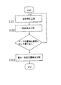
図2は半導体露光装置の概要図の一形態を示したものである。
【0005】
同図においてRは原板であるレチクル、Wは基板であるウエハ、1は投影光学系である。また、Gは位置合わせ用光学系、2は位置合わせ用照明手段、3はビームスプリッタ、4と5は結像光学系、6は撮像装置、7はA/D変換装置、8は積算装置、9は位置計測装置、10はステージ駆動手段、11は2次元に移動可能なXYステージである。
【0006】
図2ではX方向の位置を計測する位置合わせ光学系Gのみを示したが、同装置にはX方向と同様にY方向の位置を計測する不図示の位置合わせ光学系も搭載されている。図2に示した半導体露光装置はレチクルRとウエハWの相対的な位置検出して位置合わせした後、不図示の露光照明光源から露光光を照射し、レチクルR上に形成されている電子回路パターンを投影光学系1を介してXYステージ11上に載置したウエハWに投影露光する。
【0007】
次に、図2の装置におけるマスクとウエハの位置合わせについて説明する。
【0008】
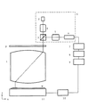
非露光光を照射する位置合わせ用照明手段2から照射された光束は、ビームスプリッタ3、レチクルR、および投影光学系1を介して、ウエハ上に形成された位置合わせ用マーク(以降アライメントマークと称する)を照明する。図3はアライメントマークを示したもので、同一形状の矩形パターンが複数個配置されている。アライメントマークから反射した光束は、再度投影光学系1、レチクルRを通ってビームスプリッタ3で反射し、結像光学系5を介して撮像装置6の撮像面上にアライメントマークの像WMを形成する。撮像装置6は形成されたマークの像WMを光電変換し、該光電変換された信号がA/D変換装置7において2次元のディジタル信号列に変換される。8は積算装置で、A/D変換装置7でディジタル信号化したウエハマーク像に対し、図3に示すように処理ウインドウWPを設定する。積算装置8はさらに該ウインドウ内においてY方向に積算処理を行い、2次元画像信号を1次元のマーク波形S(x)に変換する。図2の9は位置計測装置で、積算装置8から出力した1次元のマーク波形S(x)を用いてアライメントマークの位置を計測する。
【0009】
以上の手順を繰り返して計測したウエハ上複数個の点の位置情報や、予め不図示の方法により求めた撮像装置5とレチクルRとの相対的な位置情報に基づき、ステージ駆動手段10によりXYステージ11を移動して、マスクとウエハの位置合わせを行なう。
【0010】
次に、位置計測装置9におけるアライメントマーク位置計測方法について説明する。
【0011】
図4はアライメントマーク位置の計測方法の従来の実施形態を示したものである。図4では説明を簡単にするため、アライメントマークを1つの矩形パターンで構成した場合について述べる。アライメントマークが複数本の矩形パターンで構成されている場合は、同様の処理を繰り返せばよい。
【0012】
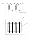
図4の一致度算出工程S102はマークの中心らしさ(一致度)を算出する工程で、予め設定してあるマーク位置計測範囲に対し繰り返し計算を行う。例えば、図5に示す様にマーク波形S(x)1に対し、一致度算出工程S102を繰り返して行うと、一致度r(x)1を求めることができる。
【0013】
続いて、従来の一致度算出工程として2つの実施形態について祥述する。
【0014】
従来の第1の実施形態は、マーク波形と予め設定してあるテンプレート波形の一致度をテンプレート位置を移動しながら算出し、一致度が最大となるとなるテンプレート位置をマーク位置とする方法である。以下、本方法をテンプレートマッチング法と呼ぶ。一致度はマーク波形とテンプレート波形の差分から計算される。マーク波形上の位置xにおける一致度r(x)は式
【0015】
【数1】

や、式
【0017】
【数2】
で求めることができる。(1)、(2)でS(x)はマーク波形、T(x)はテンプレート波形、wは一致度を算出する波形幅で、テンプレートの幅でもある。
【0019】
従来の第2の実施形態はマーク波形をある位置において対称に折り返した左右マーク波形の一致度を折り返し位置を移動しながら算出し、一致度が最大となる折り返し位置をマーク中心位置とする方法である。以下、本方法を折り返し法と呼ぶ。一致度は左右マーク波形の差分から算出することができる。マーク波形上の位置xにおける一致度r(x)は式
【0020】
【数3】
や、式
【0022】
【数4】
で求めることができる。
【0024】
図4の最大一致度位置算出工程S103はS102の一致度算出工程で算出した一致度が最大となる位置を求め、マーク中心位置とする工程である。一致度が最大となる位置は、各位置xでの一致度に対し重心計算や2次関数近似等を行うことにより、センサの分解能以下の精度で求めることができる。例えば、(5)式は重心計算式を用いいてマーク中心位置Mcを求める手法である。
【0025】
【数5】
式の中で、ssからseは予め設定済の重心計算に用いる一致度の範囲である。
【0027】
以上、位置計測装置9で行うアライメントマーク位置計測方法について述べた。説明はウエハの位置計測について行ったが、該従来の位置計測方法はマスク(またはレチクル)、ステージなどの半導体露光装置の部品やユニットの位置計測にも適用可能である。また、レチクル(またはマスク)と装置基準位置、装置部品間などの相対位置合わせにも適用することができる。
【0028】
【発明が解決しようとする課題】
しかし、半導体露光装置等で用いる位置合わせ用のマークであるアライメントマークには半導体製造過程で発生するマーク段差の不均一や、マーク上に塗布されるフォトレジストの膜厚不均一等の要因により、撮像装置に入力されるマーク波形(検出波形)に形状の変形が生じ、計測誤差が発生するという問題点があった。
【0029】
例えば、アライメントマーク段差やレジスト塗布の不均一等により、図5のように形状に変形が生じたマーク波形S(x)2が入力された場合、一致度r(x)2も変化し、一致度が最大と計算される位置に誤差が発生してしまう。従来、波形形状の変形による計測誤差は実用的に大きな問題となる量ではなかった。しかしながら位置合わせ精度向上への要望が大きくなるにつれ、該波形形状の変形による位置計測誤差を軽減する必要性が高まっている。
【0030】
以上の事実に鑑みて、本発明は、マーク波形とテンプレート波形との波形差から発生する計測誤差を軽減することを目的としている。
【0031】
【課題を解決するための手段】
請求項1の発明の位置計測方法は、
被検出物体上に形成されたマークから得られるマーク波形とテンプレート波形との一致度に基づいて該マークの位置を計測する位置計測方法において、
該マーク波形と該テンプレート波形との波形差を予め設定された関数で近似し、
該近似された関数に基づいて該マーク波形および該テンプレート波形の一方又は両方を補正し、
該補正されたマーク波形およびテンプレート波形の一方又は両方を用いて該マークの位置を求める、
ことを特徴としている。
【0032】
請求項2の発明は請求項1の発明において、
該波形差を近似する該関数の係数を、最小自乗法を用いて求める、
ことを特徴としている。
【0033】
請求項3の発明は請求項1または2の発明において、
該テンプレート波形は、ある位置に関して該マーク波形の左右いずれかの波形である、
ことを特徴としている。
【0034】
請求項4の発明は請求項1乃至3のいずれかの発明において、
該関数は、直線を表わす関数である、
ことを特徴としている。
【0035】
請求項5の発明は請求項1乃至4のいずれかの発明において、
該一方と他方との一致度又は該両方の一致度を算出し、
該一致度が最大となる該テンプレート波形の位置から該マークの位置を求める、
ことを特徴としている。
【0036】
請求項6の発明は請求項1乃至5のいずれかの発明において、
該一致度として相関係数を算出する、
ことを特徴としている。
【0037】
請求項7の発明の半導体露光装置は、
ウエハ上のアライメントマークを撮像して得られるマーク波形とテンプレート波形との一致度に基づいて該アライメントマークの位置を計測して該ウエハの位置合わせを行い、レチクル上のパターンを該ウエハ上に転写する半導体露光装置において、
該マーク波形と該テンプレート波形との波形差を予め設定された関数で近似し、
該近似された関数に基づいて該マーク波形および該テンプレート波形の一方又は両方を補正し、
該補正されたマーク波形およびテンプレート波形の一方又は両方を用いて該マークの位置を求める、
ことを特徴としている。
【0038】
請求項8の発明は請求項7の発明において、
該波形差を近似する該関数の係数を、最小自乗法を用いて求める、
ことを特徴としている。
【0039】
請求項9の発明は請求項7または8の発明において、
該補正関数は、直線を表わす関数である、
ことを特徴としている。
【0040】
請求項10の発明は請求項7乃至9のいずれかの発明において、
該一方と他方との一致度又は該両方の一致度を算出し、
該一致度が最大となる該テンプレート波形の位置から該アライメントマークの位置を求める、
ことを特徴としている。
【0041】
請求項11の発明は請求項7乃至10のいずれかの発明において、
該一致度として相関係数を算出する、
ことを特徴としている。
【0042】
請求項12の発明は請求項7乃至11のいずれかの発明において、
該テンプレート波形は、ある位置に関して該マーク波形の左右いずれかの波形である、
ことを特徴としている。
【0047】
【発明の実施の形態】
本発明をテンプレートマッチング法へ適用した後述の実施形態の場合は、被検出物体に形成したマークから得られるマーク波形(検出波形)とテンプレート波形(基準波形)との、各位置における差の自乗の和が最小となるように、マーク波形およびテンプレート波形のいずれか一方、または両方を補正する波形補正工程を行った後、一致度算出工程を行う。
【0048】
これは波形をそれぞれの位置に応じた割合で補正するのは、段差やレジスト塗布の不均一等によるマーク波形の変形が、位置により徐々に変化していく場合が多いからである。
【0049】
図6は補正の様子を示したものである。マーク波形S(x)2とテンプレートT(x)の差分を位置xに関して関数近似し、マーク波形とテンプレート波形の差が近似した誤差となるように、つまりマーク波形S(x)2を近似関数の量だけ補正したS(x)'2を作成する。
【0050】
本発明を折り返し法への適用した後述の実施形態の場合は、各折り返し位置毎に、左右マーク波形の差が最小となるように左右マーク波形のどちらかまたは両方の各値をそれぞれの位置に応じた割合で補正する波形補正工程を行った後、一致度算出工程を行う事が特徴である。折り返し法では左右いずれかのマーク波形が基準波形である。各位置での左右マーク波形の差はそれぞれの位置に対して関数近似され、左右マーク波形の差が該関数近似した誤差となるように左右マーク波形のどちらかまたは両方の各値を補正する。
【0051】
波形補正後の一致度算出工程において、テンプレートマッチング法においてはマーク波形とテンプレート波形の差分から、折り返し法においては左右マーク波形の差分から一致度を算出することについては前述した。本発明では一致度を算出工程に相関係数を導入する事により、さらにマーク波形内のレベル差および傾きを補正する効果を持たせることができる。
【0052】
相関係数の計算は算出時間は増えるものの、それぞれの値に応じた割合で波形を補正する効果がある。具体的にはテンプレートマッチング法においては、マーク波形とテンプレート波形の相関係数から一致度を算出し、折り返し法においては左右マーク波形の相関係数から一致度を算出する。
【0053】
このように、一致度算出工程の前にマーク波形のレベル差および傾きをそれぞれの位置に応じた割合で補正することにより、アライメントマークの段差やレジスト塗布の不均一等の要因で生じるマーク波形の形状変化により発生する計測誤差の軽減を実現することができる。
【0054】
以下の実施形態の位置計測方法および該位置計測法を用いた半導体露光装置の基本構成は、従来の実施形態で説明した半導体露光装置と同一でよい。従って、半導体露光装置の構成および、半導体露光装置におけるマスクとウエハの位置合わせ方法については、従来の実施形態で述べたので説明を省略し、本発明を適用した半導体露光装置におけるアライメントマークの位置計測について説明する。
【0055】
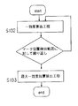
図1は本発明のアライメントマーク位置計測方法にテンプレートマッチング法を用いた実施形態である。
【0056】
図1のS101は波形補正工程で、マーク波形およびテンプレート波形のいずれかまたは両方を補正することが特徴である。例えば、マーク波形とテンプレート波形との差(波形差)を、予め設定された誤差関数で最小自乗近似法等を用いて近似し、該近似された関数の値を用いてマーク波形およびテンプレート波形のいずれか一方、または両方を補正する。
【0057】
図7はマーク波形とテンプレート波形の差をそれぞれの位置に対して直線で近似した補正方法を説明したものである。図7で縦軸はマーク波形とテンプレート波形の差、横軸は位置を示しており、テンプレートとの波形の差がある直線に近似できる分布を示していることが分かる。
【0058】
本実施形態では、図7に示した分布を直線
y=Ax+B (6)
で近似する。
【0059】
最小自乗法を用いると、直線の係数A及びBは以下の式で求める事ができる。
【0060】
【数6】
【数7】
ここでD(k)は、各位置xにおけるマーク波形とテンプレート波形の差
D(k)=S(x+k)−T(k) (9)
である。
【0063】
本実施形態ではマーク波形とテンプレート波形の差を補正するため、マーク波形とテンプレート波形の差が(6)式で近似した誤差となるようにマーク波形を補正することを特徴としている。つまり、各位置xにおいて、マーク波形の値から、近似直線の値を引いた補正後のマーク波形をS’(x)とすると、S’(x)の算出式は以下の通りとなる。
【0064】
S’(x+k)=S(x+k)−{Ak+B} (10)
(10)式では説明を簡単にするため、マーク波形とテンプレート波形の差を直線で近似する例について述べたが、マーク波形形状の変化の状態により2次関数や三角関数等の他の関数で近似しても構わない。また(10)式ではマーク波形の値を補正する実施形態について述べたが、マーク波形のかわりにテンプレート波形を補正しても構わないし、マーク波形とテンプレート波形の両方に半分づつ補正を行っても構わない。
【0065】
補正を行った後はS102の一致度算出工程で、マーク波形S’(x)に対し予め設定してあるマーク位置計測範囲でマークの中心らしさ(一致度)を繰り返し算出し、一致度r(x)の変化を計算する。
【0066】
図1のS103は最大一致度位置算出工程で、従来の実施形態と同様である。従来の実施形態では、マーク波形とテンプレート波形の差分から一致度を算出していたが、本発明は補正後のマーク波形及びテンプレート波形を用いることが違いとなっている。さらに本発明では、以下に示すマーク波形とテンプレート波形の相関係数を導入して一致度r(x)を算出してもよい。
【0067】
【数8】
ここで、Save(x)およびTave(x)は、(12)、(13)式に示すマーク波形およびテンプレート波形の平均値である。
【0069】
【数9】
相関係数で一致度を算出する方法は算出時間が増えるものの、それぞれの値に応じた割合で波形を補正する効果があるため、より一層の補正効果を実現することができる。
【0071】
以上、実施形態1におけるアライメントマークの位置計測方法について説明した。本実施形態ではウエハの位置計測と該計測値を用いてのウエハとレチクルの位置合わせへの適用について述べたが、本発明はレチクル(またはマスク)、ステージなどの半導体露光装置の部分やユニットの位置計測にも適用可能である。従って、本発明の位置計測方法はレチクル(またはマスク)と装置基準位置、装置部品間などの相対位置合わせにも適用することができる。
【0072】
実施形態2はマーク位置計測方法として折り返し法を用いた半導体露光装置に本発明を適用したものである。実施形態1と同様に半導体露光装置の構成、および半導体露光装置におけるマスクとウエハの位置合わせ方法については、従来の実施形態と同一なので説明を省略する。
【0073】
以下、実施形態1と同様に図1に基づき、本実施形態におけるマーク位置計測方法について説明する。
【0074】
図1のS101は波形補正工程で、各折り返し位置毎に左右マーク波形の差が最小となるように左右マーク波形のどちらか、または両方の各値をそれぞれの位置に応じた割合で補正することが特徴である。即ち折り返し法では左右いずれかのマーク波形が基準波形となる。各位置での左右マーク波形の差は予め定められた誤差関数でそれぞれの位置に対して関数近似され、左右マーク波形の差が該関数近似した差となるように、左右マーク波形のどちらか、または両方の各値を補正する。
【0075】
図7は左右マーク波形の差をそれぞれの位置に対して直線に近似して補正する様子を説明したものである。図7で縦軸は左右マーク波形の差、横軸は位置を示し、左右マーク波形の差がある直線で近似できる分布を示すことが分かる。
【0076】
本実施形態では、図7に示した分布を直線
y=Ax+B (14)
で近似する。
【0077】
最小自乗法を用いると、直線の係数A及びBは以下の式で求める事ができる。
【0078】
【数10】
ここでD(k)は、各位置xにおける左右マーク波形の差
D(k)=S(x−k)−S(x+k) (17)
である。
【0080】
本発明では左右マーク波形の差を補正するため、左右マーク波形の差が(14)式で近似した誤差となるようにマーク波形を補正することを特徴としている。つまり、各位置xにおいて左マーク波形の値から近似直線の値を引いて補正後のマーク波形S’(x)とすると、S’(x)の算出式は以下の通りとなる。但し、以下の補正は左マーク波形のみに行うこととする。
【0081】
S’(x+k)=S(x+k)−{Ak+B} (18)
(18)式では、説明を簡単にするため、左右マーク波形の差を直線で近似する例について述べたが、マーク波形の変化の状態により2次関数や三角関数等の他の関数で近似しても構わない。
【0082】
また、(18)式では左マーク波形の値を補正する実施形態について述べたが、左マーク波形のかわりに右マーク波形を補正しても構わないし、左右マーク波形の両方に半分づつの補正を行ってもよい。
【0083】
補正を行った後はS102の一致度算出工程で、マーク波形S’(x)に対し予め設定してあるマーク位置計測範囲でマークの中心らしさ(一致度)を繰り返し算出し、一致度r(x)の変化を計算する。
【0084】
図1のS103は最大一致度位置算出工程で、従来例の実施形態と同様である。実施形態1と同様に、相関係数を用いて一致度を算出すると、さらに精度の向上を達成することが可能である。
【0085】
以上が実施形態2におけるアライメントマーク位置計測方法である。
【0086】
実施形態2も実施形態1と同様に、ウエハの位置計測と該計測値を用いたウエハとレチクルの位置合わせへの適用について述べた。さらに本発明はレチクル(またはマスク)、ステージなどの半導体露光装置の部分やユニットの位置計測にも適用可能である。従って、本発明の位置計測方法はレチクル(またはマスク)と装置基準位置、装置部品間などの相対位置合わせにも適用することができる。
【0087】
【発明の効果】
本発明によれば、マーク波形とテンプレート波形との波形差から発生する計測誤差を軽減することができる。
【図面の簡単な説明】
【図1】 本発明を適用したアライメントマーク位置計測方法を示す図、
【図2】 半導体露光装置の概略図、
【図3】 アライメントマークの説明図、
【図4】 アライメントマーク位置計測方法の従来の実施形態を示す図、
【図5】 マーク波形の例を説明する図、
【図6】 波形補正方法の説明図、
【図7】 波形補正方法の説明図
【符号の説明】
1 投影光学系
2 位置合わせ用照明手段
3 ビームスプリッタ
4 結像光学系
5 結像光学系
6 撮像装置
7 A/D変換装置
8 積算装置
9 位置計測装置
10 ステージ駆動手段
11 XYステージ
101 波形補正工程
102 一致度算出工程
103 最大一致度位置算出工程[0001]
BACKGROUND OF THE INVENTION
The present invention relates to a position measuring method and a semiconductor exposure apparatus for measuring the position of the mark.
[0002]
[Prior art]
Precise measurement of the object position is used in various fields such as machine tools and robots, and further improvement in accuracy is required. In recent years, the degree of integration of semiconductor elements has been increasing as represented by DRAM, and the pattern size formed on the semiconductor elements by a semiconductor exposure apparatus has been further refined. Against this background, further improvement in accuracy is an important issue in the alignment process by measuring the position of the reticle and wafer, which is an essential technique of a semiconductor exposure apparatus.
[0003]
A conventional example of a semiconductor exposure apparatus and a wafer alignment method used in the exposure apparatus will be described below.
[0004]
FIG. 2 shows one form of a schematic diagram of a semiconductor exposure apparatus.
[0005]
In the figure, R is a reticle as an original plate, W is a wafer as a substrate, and 1 is a projection optical system. G is a positioning optical system, 2 is a positioning illumination means, 3 is a beam splitter, 4 and 5 are imaging optical systems, 6 is an imaging device, 7 is an A / D conversion device, 8 is an integrating device,
[0006]
Although only the alignment optical system G for measuring the position in the X direction is shown in FIG. 2, the alignment optical system (not shown) for measuring the position in the Y direction as well as the X direction is mounted on the apparatus. The semiconductor exposure apparatus shown in FIG. 2 detects and aligns the relative position of the reticle R and the wafer W, and then irradiates exposure light from an exposure illumination light source (not shown) to form an electronic circuit formed on the reticle R. The pattern is projected and exposed to the wafer W placed on the XY stage 11 via the projection
[0007]
Next, the alignment of the mask and the wafer in the apparatus of FIG. 2 will be described.
[0008]
The light beam emitted from the alignment illumination means 2 for irradiating the non-exposure light passes through the
[0009]
Based on the positional information of a plurality of points on the wafer measured by repeating the above procedure and the relative positional information of the
[0010]
Next, an alignment mark position measuring method in the
[0011]
FIG. 4 shows a conventional embodiment of the alignment mark position measuring method. In FIG. 4, a case where the alignment mark is configured by one rectangular pattern will be described in order to simplify the description. If the alignment mark is composed of a plurality of rectangular patterns, the same process may be repeated.
[0012]
The coincidence degree calculation step S102 of FIG. 4 is a step of calculating the centrality (degree of coincidence) of the mark, and repeatedly performs calculation for a preset mark position measurement range. For example, to mark waveform S (x) 1 as shown in FIG. 5, if performed repeatedly coincidence degree calculation step S102, it is possible to determine the coincidence degree r (x) 1.
[0013]
Subsequently, two embodiments will be described as a conventional coincidence calculation process.
[0014]
The first conventional embodiment is a method of calculating the degree of coincidence between a mark waveform and a preset template waveform while moving the template position, and setting the template position at which the degree of coincidence becomes the maximum as the mark position. Hereinafter, this method is referred to as a template matching method. The degree of coincidence is calculated from the difference between the mark waveform and the template waveform. The degree of coincidence r (x) at the position x on the mark waveform is expressed by the equation:
[Expression 1]
And the formula [0017]
[Expression 2]
Can be obtained. In (1) and (2), S (x) is the mark waveform, T (x) is the template waveform, w is the waveform width for calculating the degree of coincidence, and is also the width of the template.
[0019]
In the second conventional embodiment, the degree of coincidence of the left and right mark waveforms obtained by symmetrically folding back the mark waveform at a certain position is calculated while moving the folding position, and the folding position at which the degree of coincidence is maximum is used as the mark center position. is there. Hereinafter, this method is called a folding method. The degree of coincidence can be calculated from the difference between the left and right mark waveforms. The degree of coincidence r (x) at the position x on the mark waveform is expressed by the following equation:
[Equation 3]
And the formula [0022]
[Expression 4]
Can be obtained.
[0024]
The maximum coincidence position calculation step S103 in FIG. 4 is a step of obtaining a position where the coincidence calculated in the coincidence degree calculation step of S102 is maximized and setting it as the mark center position. The position where the degree of coincidence becomes maximum can be obtained with accuracy below the resolution of the sensor by performing centroid calculation, quadratic function approximation or the like on the degree of coincidence at each position x. For example, Expression (5) is a technique for obtaining the mark center position Mc using a center of gravity calculation expression.
[0025]
[Equation 5]
In the formula, ss to se are the range of coincidence used for the pre-set centroid calculation.
[0027]
The alignment mark position measuring method performed by the
[0028]
[Problems to be solved by the invention]
However, the alignment mark, which is an alignment mark used in a semiconductor exposure apparatus or the like, is caused by factors such as non-uniformity in the mark step generated in the semiconductor manufacturing process and non-uniform film thickness of the photoresist applied on the mark. There has been a problem that a shape error occurs in the mark waveform (detection waveform) input to the imaging apparatus, resulting in a measurement error.
[0029]
For example, when the mark waveform S (x) 2 whose shape has been deformed as shown in FIG. 5 due to alignment mark step or non-uniform resist coating is input, the matching degree r (x) 2 also changes and matches. An error occurs at the position where the degree is calculated to be the maximum. Conventionally, the measurement error due to the deformation of the waveform shape has not been a practically significant amount. However, as the demand for improving the alignment accuracy increases, the necessity for reducing the position measurement error due to the deformation of the waveform shape is increasing.
[0030]
In view of the above facts, the present invention aims at reducing the measurement error generated from the waveform difference between the mark waveform and the template waveform.
[0031]
[Means for Solving the Problems]
The position measuring method of the invention of
In the position measuring method for measuring the position of the mark based on the degree of coincidence between the mark waveform obtained from the mark formed on the detected object and the template waveform ,
Approximated by preset function waveform difference between the mark waveform and the template waveform,
Correcting one or both of the mark waveform and the template waveform based on the approximated function ;
Determining the position of the mark using one or both of the corrected mark waveform and template waveform ;
It is characterized by that.
[0032]
The invention of
A coefficient of the function approximating the waveform difference is determined using a least square method;
It is characterized by that.
[0033]
The invention of
The template waveform is a left or right of the waveform of the mark waveform with respect to a certain position,
It is characterized by that.
[0034]
The invention of claim 4 is the invention of any one of
The function is a function representing a straight line,
It is characterized by that.
[0035]
The invention of
Calculate the degree of coincidence between the one and the other or both ,
Obtaining the position of the mark from the position of the template waveform that maximizes the degree of coincidence ;
It is characterized by that.
[0036]
The invention of
Calculating a correlation coefficient as the degree of coincidence ,
It is characterized by that.
[0037]
A semiconductor exposure apparatus according to a seventh aspect of the invention comprises:
The alignment mark on the wafer based on the degree of coincidence between the mark waveform and the template waveform obtained by imaging by measuring the position of the alignment mark aligns of the wafer, transfers the pattern on the reticle onto the wafer in the semiconductor exposure apparatus for,
Approximated by preset function waveform difference between the mark waveform and the template waveform,
Correcting one or both of the mark waveform and the template waveform based on the approximated function ;
Determining the position of the mark using one or both of the corrected mark waveform and template waveform ;
It is characterized by that.
[0038]
The invention of claim 8 is the invention of
A coefficient of the function approximating the waveform difference is determined using a least square method;
It is characterized by that.
[0039]
The invention of
The correction function is a function representing a straight line .
It is characterized by that.
[0040]
The invention of
Calculate the degree of coincidence between the one and the other or both ,
Determining the position of the alignment mark from the position of the template waveform that the match degree is maximum,
It is characterized by that.
[0041]
The invention of claim 11 is the invention of any one of
Calculating a correlation coefficient as the degree of coincidence ,
It is characterized by that.
[0042]
The invention of claim 12 is the invention of any one of
The template waveform is a left or right of the waveform of the mark waveform with respect to a certain position,
It is characterized by that.
[0047]
DETAILED DESCRIPTION OF THE INVENTION
In the case of the later-described embodiment in which the present invention is applied to the template matching method, the square of the difference at each position between the mark waveform (detection waveform) obtained from the mark formed on the detected object and the template waveform (reference waveform) is obtained . such that the sum is minimized, after waveform correction step of correcting one or both of the mark waveform and the template waveform, performs coincidence degree calculating step.
[0048]
This is because the waveform is corrected at a ratio corresponding to each position because the deformation of the mark waveform due to a step or non-uniformity in resist coating often changes gradually depending on the position.
[0049]
FIG. 6 shows the state of correction. A function approximation is performed on the difference between the mark waveform S (x) 2 and the template T (x) with respect to the position x so that the difference between the mark waveform and the template waveform becomes an approximate error, that is, the mark waveform S (x) 2 is approximated. only to create a S (x) '2 obtained by correcting the amount of.
[0050]
In the case of the later-described embodiment in which the present invention is applied to the folding method, each value of either or both of the left and right mark waveforms is set to the respective positions so that the difference between the left and right mark waveforms is minimized for each folding position. It is characterized in that after performing a waveform correction process for correcting at a corresponding rate, a matching degree calculation process is performed. In the folding method, the left or right mark waveform is the reference waveform. The difference between the left and right mark waveforms at each position is approximated by a function with respect to each position, and either or both values of the left and right mark waveforms are corrected so that the difference between the left and right mark waveforms becomes an error that approximates the function.
[0051]
As described above, in the coincidence calculation step after waveform correction, the coincidence is calculated from the difference between the mark waveform and the template waveform in the template matching method and from the difference between the left and right mark waveforms in the folding method. In the present invention, by introducing the correlation coefficient into the coincidence calculation process, it is possible to further have an effect of correcting the level difference and the inclination in the mark waveform.
[0052]
Although the calculation of the correlation coefficient increases the calculation time, it has an effect of correcting the waveform at a rate corresponding to each value. Specifically, in the template matching method, the degree of coincidence is calculated from the correlation coefficient between the mark waveform and the template waveform, and in the aliasing method, the degree of coincidence is calculated from the correlation coefficient between the left and right mark waveforms.
[0053]
As described above, by correcting the level difference and inclination of the mark waveform at a rate corresponding to each position before the coincidence calculation step, the mark waveform generated due to factors such as uneven alignment marks and resist coating nonuniformity. It is possible to reduce the measurement error caused by the shape change.
[0054]
The basic configuration of the position measurement method and the semiconductor exposure apparatus using the position measurement method in the following embodiments may be the same as the semiconductor exposure apparatus described in the conventional embodiment. Therefore, since the configuration of the semiconductor exposure apparatus and the method for aligning the mask and wafer in the semiconductor exposure apparatus have been described in the conventional embodiments, description thereof will be omitted, and the alignment mark position measurement in the semiconductor exposure apparatus to which the present invention is applied will be omitted. Will be described.
[0055]
FIG. 1 shows an embodiment in which a template matching method is used for the alignment mark position measuring method of the present invention.
[0056]
S101 of FIG. 1 is a waveform correction process is characterized in that for correcting one or both of the mark waveform and the template waveform. For example, the difference (waveform difference) between the mark waveform and the template waveform, and approximation using the least squares approximation method in the error function that has been set in advance, the mark waveform and using the values of the function is the approximated Correct one or both of the template waveforms.
[0057]
FIG. 7 illustrates a correction method in which the difference between the mark waveform and the template waveform is approximated by a straight line with respect to each position. In FIG. 7, the vertical axis indicates the difference between the mark waveform and the template waveform, and the horizontal axis indicates the position, indicating that the distribution can be approximated to a straight line with the waveform difference from the template.
[0058]
In the present embodiment, the distribution shown in FIG. 7 is represented by a straight line y = Ax + B (6)
Approximate.
[0059]
When the least square method is used, the linear coefficients A and B can be obtained by the following equations.
[0060]
[Formula 6]
[Expression 7]
Here, D (k) is the difference between the mark waveform and the template waveform at each position x D (k) = S (x + k) −T (k) (9)
It is.
[0063]
In this embodiment, in order to correct the difference between the mark waveform and the template waveform, the mark waveform is corrected so that the difference between the mark waveform and the template waveform becomes an error approximated by equation (6). That is, assuming that the corrected mark waveform obtained by subtracting the approximate straight line value from the mark waveform value at each position x is S ′ (x), the calculation formula of S ′ (x) is as follows.
[0064]
S ′ (x + k) = S (x + k) − {Ak + B} (10)
In order to simplify the explanation in equation (10), an example in which the difference between the mark waveform and the template waveform is approximated by a straight line has been described. However, other functions such as a quadratic function and a trigonometric function are used depending on the change in the mark waveform shape. You may approximate. In addition, although the embodiment of correcting the value of the mark waveform has been described in equation (10), the template waveform may be corrected instead of the mark waveform, or both the mark waveform and the template waveform may be corrected in half. I do not care.
[0065]
After the correction, in the coincidence degree calculating step of S102, the centrality (coincidence degree) of the mark is repeatedly calculated in the mark position measurement range set in advance for the mark waveform S ′ (x), and the coincidence degree r ( Calculate the change in x).
[0066]
S103 in FIG. 1 is a maximum matching position calculation step, which is the same as in the conventional embodiment. In the conventional embodiment, the degree of coincidence is calculated from the difference between the mark waveform and the template waveform. However, the present invention is different in that the corrected mark waveform and template waveform are used. Furthermore, in the present invention, the degree of coincidence r (x) may be calculated by introducing a correlation coefficient between a mark waveform and a template waveform shown below.
[0067]
[Equation 8]
Here, S ave (x) and T ave (x) are average values of the mark waveform and the template waveform shown in the equations (12) and (13).
[0069]
[Equation 9]
Although the method for calculating the degree of coincidence using the correlation coefficient increases the calculation time, it has the effect of correcting the waveform at a rate corresponding to each value, and thus a further correction effect can be realized.
[0071]
The alignment mark position measurement method in the first embodiment has been described above. In the present embodiment, the position measurement of the wafer and the application to the alignment of the wafer and the reticle using the measurement values have been described. However, the present invention relates to a part or unit of a semiconductor exposure apparatus such as a reticle (or mask) or a stage. It can also be applied to position measurement. Therefore, the position measurement method of the present invention can also be applied to relative alignment between a reticle (or mask) and an apparatus reference position, between apparatus parts, and the like.
[0072]
In the second embodiment, the present invention is applied to a semiconductor exposure apparatus using a folding method as a mark position measuring method. As in the first embodiment, the configuration of the semiconductor exposure apparatus and the method for aligning the mask and the wafer in the semiconductor exposure apparatus are the same as those in the conventional embodiment, and a description thereof will be omitted.
[0073]
Hereinafter, the mark position measuring method according to the present embodiment will be described based on FIG. 1 as in the first embodiment.
[0074]
S101 in FIG. 1 is a waveform correction step, and corrects each value of either or both of the left and right mark waveforms at a ratio corresponding to each position so that the difference between the left and right mark waveforms is minimized at each folding position. Is a feature. That is, in the folding method, the left or right mark waveform is the reference waveform. The difference between the left and right mark waveforms at each position is approximated with respect to each position by a predetermined error function, so that the difference between the left and right mark waveforms is the difference obtained by approximating the function. Or correct both values.
[0075]
FIG. 7 illustrates the manner in which the difference between the left and right mark waveforms is corrected by approximating a straight line with respect to each position. In FIG. 7, the vertical axis indicates the difference between the left and right mark waveforms, the horizontal axis indicates the position, and it can be seen that the distribution can be approximated by a straight line with the difference between the left and right mark waveforms.
[0076]
In the present embodiment, the distribution shown in FIG. 7 is represented by a straight line y = Ax + B (14)
Approximate.
[0077]
When the least square method is used, the linear coefficients A and B can be obtained by the following equations.
[0078]
[Expression 10]
Here, D (k) is the difference between the left and right mark waveforms at each position x D (k) = S (x−k) −S (x + k) (17)
It is.
[0080]
In the present invention, in order to correct the difference between the left and right mark waveforms, the mark waveform is corrected so that the difference between the left and right mark waveforms becomes an error approximated by the equation (14). That is, if the approximated straight line value is subtracted from the left mark waveform value at each position x to obtain the corrected mark waveform S ′ (x), the calculation formula of S ′ (x) is as follows. However, the following correction is performed only on the left mark waveform.
[0081]
S ′ (x + k) = S (x + k) − {Ak + B} (18)
In formula (18), for the sake of simplicity, an example has been described in which the difference between the left and right mark waveforms is approximated by a straight line. It doesn't matter.
[0082]
Further, although the embodiment for correcting the value of the left mark waveform has been described in the equation (18), the right mark waveform may be corrected instead of the left mark waveform, and half correction is performed for both the left and right mark waveforms. You may go.
[0083]
After the correction, in the coincidence degree calculating step of S102, the centrality (coincidence degree) of the mark is repeatedly calculated in the mark position measurement range set in advance for the mark waveform S ′ (x), and the coincidence degree r ( Calculate the change in x).
[0084]
S103 in FIG. 1 is a maximum matching score position calculation step, which is the same as that in the conventional example. As in the first embodiment, when the degree of coincidence is calculated using the correlation coefficient, further improvement in accuracy can be achieved.
[0085]
The above is the alignment mark position measurement method in the second embodiment.
[0086]
In the second embodiment, as in the first embodiment, the position measurement of the wafer and the application to the alignment of the wafer and the reticle using the measurement values have been described. Further, the present invention can be applied to position measurement of a part or unit of a semiconductor exposure apparatus such as a reticle (or mask) or a stage. Therefore, the position measurement method of the present invention can also be applied to relative alignment between a reticle (or mask) and an apparatus reference position, between apparatus parts, and the like.
[0087]
【The invention's effect】
According to the present invention, Ru can and this to reduce the measurement error generated from the waveform difference between the mark waveform and the template waveform.
[Brief description of the drawings]
FIG. 1 is a diagram showing an alignment mark position measuring method to which the present invention is applied;
FIG. 2 is a schematic diagram of a semiconductor exposure apparatus;
FIG. 3 is an explanatory diagram of an alignment mark,
FIG. 4 is a diagram showing a conventional embodiment of an alignment mark position measuring method;
FIG. 5 is a diagram for explaining an example of a mark waveform;
FIG. 6 is an explanatory diagram of a waveform correction method;
[Figure 7] Explanation of waveform correction method [Explanation of symbols]
DESCRIPTION OF
Claims (12)
該マーク波形と該テンプレート波形との波形差を予め設定された関数で近似し、
該近似された関数に基づいて該マーク波形および該テンプレート波形の一方又は両方を補正し、
該補正されたマーク波形およびテンプレート波形の一方又は両方を用いて該マークの位置を求める、
ことを特徴とする位置計測方法。In the position measuring method for measuring the position of the mark based on the degree of coincidence between the mark waveform obtained from the mark formed on the detected object and the template waveform ,
Approximated by preset function waveform difference between the mark waveform and the template waveform,
Correcting one or both of the mark waveform and the template waveform based on the approximated function ;
Determining the position of the mark using one or both of the corrected mark waveform and template waveform ;
A position measurement method characterized by that.
ことを特徴とする請求項1に記載の位置計測方法。 A coefficient of the function approximating the waveform difference is determined using a least square method;
The position measuring method according to claim 1.
ことを特徴とする請求項1または2に記載の位置計測方法。The template waveform is a left or right of the waveform of the mark waveform with respect to a certain position,
The position measuring method according to claim 1 or 2, wherein
ことを特徴とする請求項1乃至3のいずれかに記載の位置計測方法。 The function is a function representing a straight line,
The position measuring method according to claim 1, wherein
該一致度が最大となる該テンプレート波形の位置から該マークの位置を求める、
ことを特徴とする請求項1乃至4のいずれかに記載の位置計測方法。 Calculate the degree of coincidence between the one and the other or both ,
Obtaining the position of the mark from the position of the template waveform that maximizes the degree of coincidence ;
The position measuring method according to claim 1, wherein
ことを特徴とする請求項1乃至5のいずれかに記載の位置計測方法。 Calculating a correlation coefficient as the degree of coincidence ,
The position measuring method according to claim 1, wherein
該マーク波形と該テンプレート波形との波形差を予め設定された関数で近似し、
該近似された関数に基づいて該マーク波形および該テンプレート波形の一方又は両方を補正し、
該補正されたマーク波形およびテンプレート波形の一方又は両方を用いて該マークの位置を求める、
ことを特徴とする半導体露光装置。 The alignment mark on the wafer based on the degree of coincidence between the mark waveform and the template waveform obtained by imaging by measuring the position of the alignment mark aligns of the wafer, transfers the pattern on the reticle onto the wafer in the semiconductor exposure apparatus for,
Approximated by preset function waveform difference between the mark waveform and the template waveform,
Correcting one or both of the mark waveform and the template waveform based on the approximated function ;
Determining the position of the mark using one or both of the corrected mark waveform and template waveform ;
A semiconductor exposure apparatus.
ことを特徴とする請求項7に記載の半導体露光装置。 A coefficient of the function approximating the waveform difference is determined using a least square method;
The semiconductor exposure apparatus according to claim 7 .
ことを特徴とする請求項7または8に記載の半導体露光装置。The correction function is a function representing a straight line .
The semiconductor exposure apparatus according to claim 7 or 8, wherein
該一致度が最大となる該テンプレート波形の位置から該アライメントマークの位置を求める、
ことを特徴とする請求項7乃至9のいずれかに記載の半導体露光装置。Calculate the degree of coincidence between the one and the other or both ,
Determining the position of the alignment mark from the position of the template waveform that the match degree is maximum,
The semiconductor exposure apparatus according to any one of claims 7 to 9, characterized in that.
ことを特徴とする請求項7乃至10のいずれかに記載の半導体露光装置。 Calculating a correlation coefficient as the degree of coincidence ,
11. The semiconductor exposure apparatus according to claim 7 , wherein
ことを特徴とする請求項7乃至11のいずれかに記載の半導体露光装置。The template waveform is a left or right of the waveform of the mark waveform with respect to a certain position,
The semiconductor exposure apparatus according crab of claims 7 to 11, characterized in that.
Priority Applications (2)
| Application Number | Priority Date | Filing Date | Title |
|---|---|---|---|
| JP08405299A JP4046884B2 (en) | 1999-03-26 | 1999-03-26 | Position measuring method and semiconductor exposure apparatus using the position measuring method |
| US09/533,690 US6538260B1 (en) | 1999-03-26 | 2000-03-23 | Position measuring method, and semiconductor device manufacturing method and apparatus using the same |
Applications Claiming Priority (1)
| Application Number | Priority Date | Filing Date | Title |
|---|---|---|---|
| JP08405299A JP4046884B2 (en) | 1999-03-26 | 1999-03-26 | Position measuring method and semiconductor exposure apparatus using the position measuring method |
Publications (3)
| Publication Number | Publication Date |
|---|---|
| JP2000275010A JP2000275010A (en) | 2000-10-06 |
| JP2000275010A5 JP2000275010A5 (en) | 2006-05-18 |
| JP4046884B2 true JP4046884B2 (en) | 2008-02-13 |
Family
ID=13819743
Family Applications (1)
| Application Number | Title | Priority Date | Filing Date |
|---|---|---|---|
| JP08405299A Expired - Fee Related JP4046884B2 (en) | 1999-03-26 | 1999-03-26 | Position measuring method and semiconductor exposure apparatus using the position measuring method |
Country Status (2)
| Country | Link |
|---|---|
| US (1) | US6538260B1 (en) |
| JP (1) | JP4046884B2 (en) |
Families Citing this family (9)
| Publication number | Priority date | Publication date | Assignee | Title |
|---|---|---|---|---|
| JP4178875B2 (en) * | 2002-08-22 | 2008-11-12 | 株式会社ニコン | Mark position detection device, mark position detection method, overlay measurement device, and overlay measurement method |
| TWI236562B (en) * | 2002-11-21 | 2005-07-21 | Hitachi Int Electric Inc | A method of detecting a pattern and an apparatus thereof |
| JP4101076B2 (en) * | 2003-02-06 | 2008-06-11 | キヤノン株式会社 | Position detection method and apparatus |
| US7728953B2 (en) * | 2004-03-01 | 2010-06-01 | Nikon Corporation | Exposure method, exposure system, and substrate processing apparatus |
| JP4760705B2 (en) * | 2004-03-01 | 2011-08-31 | 株式会社ニコン | Pre-measurement processing method, exposure system, and substrate processing apparatus |
| JP4603814B2 (en) * | 2004-04-23 | 2010-12-22 | キヤノン株式会社 | Exposure apparatus, focus position detection apparatus and methods thereof, and device manufacturing method |
| JP3962736B2 (en) * | 2004-10-08 | 2007-08-22 | キヤノン株式会社 | Exposure apparatus and device manufacturing method |
| US7702157B2 (en) | 2005-03-30 | 2010-04-20 | Kabushiki Kaisha Toshiba | Pattern evaluation method, pattern matching method and computer readable medium |
| JP5507875B2 (en) | 2009-04-14 | 2014-05-28 | キヤノン株式会社 | Exposure apparatus, exposure method, and device manufacturing method |
Family Cites Families (2)
| Publication number | Priority date | Publication date | Assignee | Title |
|---|---|---|---|---|
| US5543921A (en) * | 1989-05-08 | 1996-08-06 | Canon Kabushiki Kaisha | Aligning method utilizing reliability weighting coefficients |
| JP3634487B2 (en) | 1996-02-09 | 2005-03-30 | キヤノン株式会社 | Alignment method, alignment apparatus, and exposure apparatus |
-
1999
- 1999-03-26 JP JP08405299A patent/JP4046884B2/en not_active Expired - Fee Related
-
2000
- 2000-03-23 US US09/533,690 patent/US6538260B1/en not_active Expired - Fee Related
Also Published As
| Publication number | Publication date |
|---|---|
| JP2000275010A (en) | 2000-10-06 |
| US6538260B1 (en) | 2003-03-25 |
Similar Documents
| Publication | Publication Date | Title |
|---|---|---|
| JP3002351B2 (en) | Positioning method and apparatus | |
| JPH0562880A (en) | Exposure equipment | |
| US20180143539A1 (en) | Exposure apparatus, exposure method, and device manufacturing method | |
| JPH07335524A (en) | Alignment method | |
| JPH0945609A (en) | Best focus determination method and exposure condition determination method using the same | |
| JP2000021738A (en) | Position detecting device and position detecting method using the same | |
| JP4046884B2 (en) | Position measuring method and semiconductor exposure apparatus using the position measuring method | |
| JP3595707B2 (en) | Exposure apparatus and exposure method | |
| WO2022106182A1 (en) | Metrology system and lithographic system | |
| JP3315540B2 (en) | Position measuring apparatus, positioning apparatus, exposure apparatus, and device manufacturing method | |
| WO2007038134A2 (en) | Method of aligning a particle-beam-generated pattern to a pattern on pre-patterned substrate | |
| JPH09166416A (en) | Reticle pattern relative displacement amount measuring method and reticle pattern relative displacement amount measuring device | |
| KR20200140714A (en) | Alignment apparatus, alignment method, lithography apparatus, and method of manufacturing article | |
| JP2005011976A (en) | Position detection method | |
| KR20220122489A (en) | Detection apparatus, detection method, program, lithography apparatus, and article manufacturing method | |
| JP4101076B2 (en) | Position detection method and apparatus | |
| JP3600882B2 (en) | Alignment method, exposure method, element manufacturing method, and alignment apparatus and exposure apparatus | |
| JP2830462B2 (en) | Alignment apparatus, exposure apparatus, and method of manufacturing semiconductor device using the same | |
| JP3894505B2 (en) | Position detection method, position detection apparatus, semiconductor exposure apparatus, and semiconductor manufacturing method | |
| JPH10326739A (en) | Positioning method and exposure method | |
| JP3286124B2 (en) | Alignment apparatus and method | |
| WO2021249711A1 (en) | Metrology method, metrology apparatus and lithographic apparatus | |
| JPH1154418A (en) | Signal waveform correction method and device | |
| JPH07211612A (en) | Projection exposure device | |
| JPH1152545A (en) | Reticle, pattern transferred thereby, and method of aligning reticle with semiconductor wafer |
Legal Events
| Date | Code | Title | Description |
|---|---|---|---|
| A521 | Request for written amendment filed |
Free format text: JAPANESE INTERMEDIATE CODE: A523 Effective date: 20060324 |
|
| A621 | Written request for application examination |
Free format text: JAPANESE INTERMEDIATE CODE: A621 Effective date: 20060324 |
|
| A977 | Report on retrieval |
Free format text: JAPANESE INTERMEDIATE CODE: A971007 Effective date: 20070628 |
|
| A131 | Notification of reasons for refusal |
Free format text: JAPANESE INTERMEDIATE CODE: A131 Effective date: 20070703 |
|
| A521 | Request for written amendment filed |
Free format text: JAPANESE INTERMEDIATE CODE: A523 Effective date: 20070903 |
|
| TRDD | Decision of grant or rejection written | ||
| A01 | Written decision to grant a patent or to grant a registration (utility model) |
Free format text: JAPANESE INTERMEDIATE CODE: A01 Effective date: 20071113 |
|
| A61 | First payment of annual fees (during grant procedure) |
Free format text: JAPANESE INTERMEDIATE CODE: A61 Effective date: 20071121 |
|
| FPAY | Renewal fee payment (event date is renewal date of database) |
Free format text: PAYMENT UNTIL: 20101130 Year of fee payment: 3 |
|
| R150 | Certificate of patent or registration of utility model |
Free format text: JAPANESE INTERMEDIATE CODE: R150 |
|
| FPAY | Renewal fee payment (event date is renewal date of database) |
Free format text: PAYMENT UNTIL: 20101130 Year of fee payment: 3 |
|
| FPAY | Renewal fee payment (event date is renewal date of database) |
Free format text: PAYMENT UNTIL: 20111130 Year of fee payment: 4 |
|
| FPAY | Renewal fee payment (event date is renewal date of database) |
Free format text: PAYMENT UNTIL: 20121130 Year of fee payment: 5 |
|
| FPAY | Renewal fee payment (event date is renewal date of database) |
Free format text: PAYMENT UNTIL: 20131130 Year of fee payment: 6 |
|
| LAPS | Cancellation because of no payment of annual fees |