JP4046825B2 - Data transfer device - Google Patents
Data transfer device Download PDFInfo
- Publication number
- JP4046825B2 JP4046825B2 JP36153397A JP36153397A JP4046825B2 JP 4046825 B2 JP4046825 B2 JP 4046825B2 JP 36153397 A JP36153397 A JP 36153397A JP 36153397 A JP36153397 A JP 36153397A JP 4046825 B2 JP4046825 B2 JP 4046825B2
- Authority
- JP
- Japan
- Prior art keywords
- transfer
- data
- time
- dma
- size
- Prior art date
- Legal status (The legal status is an assumption and is not a legal conclusion. Google has not performed a legal analysis and makes no representation as to the accuracy of the status listed.)
- Expired - Fee Related
Links
Images
Landscapes
- Debugging And Monitoring (AREA)
- Bus Control (AREA)
Description
【0001】
【発明の属する技術分野】
本発明は、大容量のデータをDMA(Direct Memory Access )を用いて転送するデータ転送装置に関する。
【0002】
【従来の技術】
従来から大容量のデータ転送を高速に行うには、DMA転送は必須の技術である。この種のデータ転送を高速に行う技術としては、バスマスタデバイスでバスを継続的に使用するバーストモード方式が一般的である。
【0003】
近年、このバースト転送の性能向上のために、クロックと同期することによって、高速転送を行えるSDRAM(Synchronous DRAM)を用いる技術がある。
【0004】
【発明が解決しようとする課題】
しかしながら、高速転送が可能なSDRAMは、クロックパルスと同期するため、電圧降下などによるハードウェアのわずかなタイミングの狂いが生じた場合でも、データ転送エラーという致命的な欠陥が発生しやすく、データに影響を及ぼすという問題点がある。
【0005】
また、転送エラーを起こした場合、必要なデータサイズの転送が終了しないので、ホストCPUは、終了を認識できない。このような場合は、DMAコントローラを停止させ、SDRAMのモード切り換えを指示する必要がある。このモード切り換え処理を行わず、他のメモリアクセスを実行すると、ローカルバスがロックし、システム全体がハングアップする場合がある。
【0006】
さらに、ホストCPUやDMAコントローラの制限によって、14MBのDMA転送を一度に実行できない場合がほとんどであり、また、バーストモード方式は、転送時間が長くなると、バスを占有する時間が長いため、ホストCPU上で動作するOS(Operating System )やアプリケーションのレスポンスが悪くなる傾向がある。
【0007】
そこで、本発明の目的は、データのDMA転送における総転送時間を短縮させ、最適なバス使用効率を設定することが可能なデータ転送装置を提供することにある。
【0008】
【課題を解決するための手段】
本発明は、データを複数に分割することによって、DMA転送を繰り返して行うデータ転送装置であって、前記データのDMA転送の転送時間を計測するタイマーと、前記タイマーによって計測したDMA転送の1回当たりの転送時間を転送終了毎に測定する転送時間測定手段と、該測定された転送時間に基づいて、今回と前回の単位バイト数あたりの転送時間を比較し、前回より今回の単位バイト数あたりの転送時間が短くなった場合は、今回よりデータ転送サイズを大きくしてDMA転送させ、前回より今回の単位バイト数当たりの転送時間が長くなった場合は前回のデータ転送サイズを最適な転送サイズとして決定する転送サイズ決定手段とを具え、該決定されたデータ転送サイズに従ってDMA転送を繰り返して行うことによって、データ転送装置を構成する。
【0010】
前記データの転送エラーが生じた場合、起動したタイマーのタイムアウトにより異常を検知する手段と、該異常の検知によって前記データのDMA転送を停止させる手段とをさらに具えることができる。
【0012】
本発明は、データを複数に分割することによって、DMA転送を繰り返して行うデータ転送方法であって、DMA転送の1回当たりの転送時間を転送終了毎に測定する工程と、該測定された転送時間に基づいて、今回と前回の単位バイト数あたりの転送時間を比較し、前回より今回の単位バイト数あたりの転送時間が短い場合は、データ転送サイズを大きくしてDMA転送させ、前回より今回の単位バイト数当たりの転送時間が長くなった場合は前回のデータ転送サイズを最適な転送サイズとして決定する工程とを具え、該決定されたデータ転送サイズに従ってDMA転送を繰り返して行うことによって、データ転送方法を提供する。
【0014】
前記データの転送エラーが生じた場合、起動したタイマーのタイムアウトにより異常を検知する工程と、該異常の検知によって前記データのDMA転送を停止させる工程とをさらに具えることができる。
【0018】
前記データの転送エラーが生じた場合、起動させたタイマーのタイムアウトにより異常を検知させ、該異常の検知によって前記データのDMA転送を停止させることができる。
【0019】
【発明の実施の形態】
以下、図面を参照して、本発明の実施の形態を詳細に説明する。
【0020】
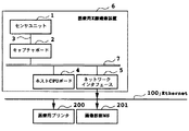
図2は、大画面固体撮像素子を備えた医療用のX線撮影装置6のシステム構成例を示す。このX線撮影装置6は、LAN100と双方向通信可能に接続されている。このLAN100としては、例えばEthenet等の病院内に張り巡らされたネットワークを想定できる。
【0021】
本例では、X線撮影装置6内におけるデータ転送処理を例に挙げる。
【0022】
X線撮影装置6において、大画面固体撮像素子を含むセンサユニット1と、撮影した画像データを蓄えるキャプチャボード2とが、画像転送専用のバス3を介して接続されている。キャプチャボード2上に転送された画像データは、さらにPCIバス7を通じて、ホストCPUボード4上に転送され、画像処理後、ネットワークインターフェース5を通じて、LAN100に接続された外部装置、例えば、医療用のプリンタ200や、他の診断装置201に転送され、医療用の画像診断に利用される。
【0023】
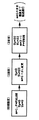
図1は、図2のX線撮影装置6におけるデータ転送処理部の構成を示す。
【0024】
このデータ転送処理部は、キャプチャボード2と、ホストCPUボード4とのシステムによって構成される。
【0025】
キャプチャボード2において、11は、ボード内の処理を統括制御するためのローカルCPUである。12は、ローカルCPU11と、ホストCPU20との通信に使用するためのDPRAMである。13は、センサユニット1からデータが入力され記憶されるSDRAMである。14は、SDRAM13のモードを切り替えるモードレジスタである。15は、SDRAM13に入力される基準クロック(CLK)である。16は、SDRAM13からのデータが入力されるFIFOメモリである。17は、PCIバスインターフェースである。このPCIバスインターフェース17内には、FIFOメモリ16内のデータのDMA転送制御を行うためのDMAコントローラ(DMAC)18が設けられている。
【0026】
ホストCPUボード4において、20は、本発明に係る図7〜図9のDMA処理を実行するためのホストCPUである。なお、本例では、ホストCPU18上で動作するOS(オペレーティングシステム)として、WindowsNTを採用している。21は、FIFOメモリ16からDMA転送されたデータが入力されるホストメモリである。22は、本発明に係る図7〜図9の制御プログラム22aが記憶されるRAMである。23は、DMA処理の際に用いられるマップレジスタである。24は、PCIバスインターフェースである。25は、キャッシュメモリである。なお、制御プログラム22aは、RAM22の他に、ROM(図示せず)に記憶したり、また、別体として、フロッピーディスク等の記憶媒体に記憶してもよい。
【0027】
以下、データ転送処理部の動作について説明する。
【0028】
データ転送処理部は、DMA転送の設定とともにタイマー(制御プログラム22aにより実行されるソフト的な手段であるが、ハード的な手段でも構成が可能である)を起動し、DMA終了割込み毎に転送に要した転送時間と転送バイト数を記憶する。
【0029】
異常が生じた場合には、タイマーのタイムアウト割込みが入るので、DMA転送を停止してバスの開放およびSDRAM13のモード切り換えをするとともに、転送異常をユーザに通知することができる。
【0030】
正常時には、次のDMA設定とタイマーを初期化し、以後すべてのデータ転送を終了するまで繰り返す。
【0031】
以上の基本シーケンスを用いてデータ転送を繰り返すが、ホストCPU20のクロックバスのメモリコントローラのウェイト時間、メモリの速度や種類などハードウェアによって、DMA転送の時間が異なる。すなわち、一般にはDMA転送を設定するオーバヘッドを最小にする方が効率良く転送ができるはずだが、ハードウェアの組み合わせを変えて転送サイタルを計測すると、1度に転送するデータサイズと割込み回数の組み合わせにおいて、転送時間が異なる。
【0032】
(メモリ空間)
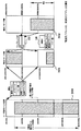
次に、DMA転送に係るメモリ空間を、図3に基づいて説明する。
【0033】
X線撮影装置6を制御するユーザプロセスは、OS上の仮想メモリ空間で動作しており、撮影データを画像処理するために14MB(メガバイト)の画像データをキャプチャボード2上のSDRAM13からホストメモリ21にDMA転送する。
【0034】
しかし、SDRAM13、DMAコントローラ18、ホストメモリ21などは、物理メモリ空間でアドレスを指定して動作しているため、ユーザプロセスヘデータ転送を実現するためには、図3に示すように、ユーザ仮想メモリ300と、物理メモリ301と、論理メモリ302との間においてメモリアドレスの変換が必要となる。この図3は、全転送要求されたバイト数Br に対して、各アドレスで示す所定サイズのブロックに分割してデータを転送する例である。
【0035】
ここで、ホストCPU20の一例としてPentiumを用いた場合には、1度にアクセス可能なサイズは4KBのページサイズという制限があるが、WindowsNTには、ホストメモリ21を論理的にOSの空間内に連続領域に割り付けることで、データ転送を1度のDMA起動に対して行う機能がある。この論理的なアドレス変換を行うのがマップレジスタであり、m個使用して、4×mKB単位でバースト転送を可能にしている。
【0036】
そして、SDRAM13のモードをモードレジスタ14で切り替え、バースト転送を行うために、ローカルCPU11は、FIFOメモリ16にデータを入れる初期化を行う。その後、PCIバスIインターフェース17に内蔵されたDMAコントローラ18が、FIFO16からホストメモリ19へデータを順次バースト転送するだけの処理になる。このとき、ローカルCPU11は、そのデータ転送中においても、他のプロセスを実行できる。また、ホストCPU20は、所定のDMAサイズに分割されたデータに対して割り込み処理を行い、次のDMA転送の設定および起動以外は、他のプロセスを実行することができる。
【0037】
(実験例)
次に、センサユニット1で撮影した14MBの画像データをDMA転送するために、分割するサイズについて考える。
【0038】
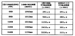
図4は、マップレジスタ23の個数を変え、1回のDMA転送のサイズを変化させて、14MB(ただし、1MB=1024KB)の画像データ全体の転送時間を計測した一例である。
【0039】
転送サイズを規定するマップレジスタ23の個数がm=4のときは、(14×1024)/16KB=896回のDMA起動および割込み後処理などのI/O処理を行わなければならない。また、m=16のときは、224回のI/O処理になる。
【0040】
しかしながら、OSの論理的連続メモリ空間にあるDMA転送されたデータを、仮想メモリ空間にあるユーザプロセスに対してデータを渡すためには、DMAコントローラ18内のキャッシュメモリ、および、ホストメモリ21内の論理空間あるいはホストCPUボード4上のキャッシュメモリ25を明示的にメモリフラッシュ(キャッシュメモリ上のデータを吐き出すためのメモリコピー)する必要がある。このメモリフラッシュ中は、次のDMA転送を行えないため、PCIバス7上は遊んでいる状態が継続し、メモリフッシュ終了後に次のDMA転送を起動できる。
【0041】
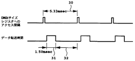
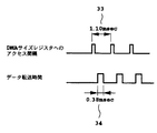
図5および図6は、回路上の信号線の状態を示す。図5は、64KB単位でDMA転送を行う場合の例である。30は、DMA転送サイズのレジスタにアクセスする時間を計測したものである。1回の転送について実際にバースト転送している転送時間は31のように短く、30から31を引いた32の部分が、転送終了割り込み後の処理になる。このとき、割り込みの後処理時間比は、
【0042】
【数1】

となる。
【0044】
また、図6は、16KB単位でDMA転送を行う場合の例である。このとき、割り込みの後処理時間比は、
【0045】
【数2】
となる。この場合、割込み後処理に時間がかかっているが、その割合が図5に比べて72%から約65%と少なくなっている。この後処理時間のほとんどがメモリフラッシュにかかっていることから、DMA転送先であるOSの論理空間がキャッシュ上にある場合に、キャッシュメモリからホストメモリ21へのメモリコピーになるため、高速に転送できると推測できる。
【0047】
以上の実験結果から、CPUクロック、バスクロック、メモリスピード、メモリアクセスウェイト、キャッシュサイズなどのハードウェア構成によって、1度にDMA転送を行う最適なサイズ、すなわち、マップレジスタ23の個数mが異なる結果になる。
【0048】
すなわち、ホストCPU20やホストメモリ21が十分に速い場合、さらにメモリアクセスウェイトが小さい場合やキャッシュメモリ25が多い場合は、DMA転送の起動および割込み後処理にかかるCPUオーバヘッドが多くても、PCIバス7の使用率を高める方が全体の転送時間を短くすることができる。一方、このオーバヘッドが多くなりすぎると、ホストCPU18が遅い場合や、チップセットの性能により、かえって転送時間がかかる結果になる。
【0049】
(DMA転送処理)
次に、DMA転送の処理を、図7〜図11に基づいて説明する。以下に示す処理は、ホストCPU20が制御プログラム22aを用いて行う制御例である。
【0050】
本処理では、画像データを複数に分割してDMA転送を繰り返して行う場合において、自動的に最適な転送サイズに近づける処理を行う。
【0051】
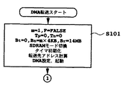
まず、図7に示すように、ステップS101において、ユーザプロセスからの要求により、初期化処理を行う。この場合、係数は、以下のような内容とする。
【0052】
m:マップレジスタの個数
F:最適な転送サイズが決定済か否かを示すフラグ
Tp:前回のDMA転送に要した単位バイト数当たり(ここでは4KB)の転送時間
Tn:今回のDMA転送に要した単位バイト数当たり(ここでは4KB)の転送時間
t:今回のDMA転送に要した転送時間
Bn:今回のDMA転送に要したバイト数
Bt:現在までの転送済のバイト数
Br:全転送要求されたバイト数
また、転送先アドレスを計算し、DMA転送の設定および起動を行う。これにより、タイマーがスタートし、FIFOメモリ16からホストメモリ21への画像データのDMA転送が開始される。
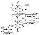
【0053】
次に、図8に示すように、ステップS102では、DMA終了割込み処理に入る。そして、ステップS103では、DMAコントローラ18がDMA転送処理終了を示す割り込み信号を発生したかをチェックする。
【0054】
DMA終了割り込みを発生した場合には、ステップS104に進む。ステップS104では、タイマーを停止し、DMA転送に要した転送時間tを記憶する。
ステップS105では、現在までに転送済のバイト数Btを算出する。
【0055】
ステップS106では、現在までの転送済のバイト数Btが、全転送要求されたバイト数Brを超えているか否かをチェックする。
【0056】
ステップS106において、現在までのバイト数Btが全バイト数Brを超えた場合は、ステップS107に進み、SDRAM13のモード切り換えを行う。そして、ステップS108にて、DMA転送を正常な状態で終了する。
【0057】
一方、現在までのバイト数Btが全バイト数Brを超えていない場合は、図9に示すステップS110に進む。ステップS110以降の処理は、最適な転送サイズを決定する処理である。
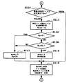
【0058】
ステップS110では、画像データの転送サイズが最適な転送サイズになっているか否かをチェックする。最適な転送サイズになっていない場合には、ステップS111に進む。
【0059】
ステップS111では、単位バイト数当たりの転送時間Tpを算出する。そして、ステップS112に進み、前回の転送時間が有効か否かをチェックする。
【0060】
ステップS112において、前回の転送時間が有効でない場合は、ステップS113に進み、個数mと、前回の転送時間Tpとの値を入れ替える。一方、前回の転送時間が有効である場合は、ステップS114に進み、前回の転送時間Tpと今回の転送時間Tnとを比較する。
【0061】
ステップS114において、今回の転送時間Tnが前回の転送時間Tpよりも短い場合は、ステップS113に進む。一方、今回の転送時間Tnが前回の転送時間Tpよりも長い場合は、ステップS115に進み、個数mを入れ替えると共に、フラグFをTRUEとすることにより、最適な転送サイズが決定される。
【0062】
その後、ステップS116に進む。このステップS116は、初期ルーチンのステップS101に対応するものである。この場合、今回の転送バイト数Btを新たに算出する。そして、DMA転送の設定および起動を行い、タイマーをスタートさせて、前回と同様に、FIFOメモリ16からホストメモリ21への画像データのDMA転送を開始する。以後、ステップS102に進み、同様な処理を繰り返す。
【0063】
また、ステップS110において、最適な転送サイズになっていた場合には、ステップS116に直接進んで処理を続行する。
【0064】
以上述べたように、最適な転送サイズを動的に探しながら、DMA転送を繰り返して行う。
【0065】
また、万一、DMAコントローラ18等のハードウェアの不具合が生じた場合には、ステップS103において、DMA転送処理終了を示す割り込みがないと判断して、ステップS201に進み、DMAタイムアウト処理を実行する。
【0066】
ステップS201では、タイマーを停止し、SDRAM13のモード切り換えを行う。そして、ステップS202に進んで、ユーザに異常状態を通知し、全ての処理を終了する(ステップS203)。このようなタイムアウト処理により、システム全体を誤動作させることなく、ユーザに異常を通知し、保守点検を促すことができる。
【0067】
また、図10〜図11は、上述した最適な転送サイズを決定する処理を模式的に示したものである。
【0068】
図10の例では、初期設定の後、2回目の処理で最適な転送サイズを決定し、以後m=1として最後の処理まで転送処理を続行する。
【0069】
図11の例では、初期設定の後、4回目の処理で最適な転送サイズを決定し、以後m=4として最後の処理まで転送処理を続行する。
【0070】
なお、本発明は、複数の機器から構成されるシステムに適用しても、1つの機器からなる装置に適用してもよい。また、本発明はシステム或いは装置にプログラムを供給することによって達成される場合にも適用できることはいうまでもない。この場合、本発明を達成するためのソフトウェアによって表されるプログラムを格納した記憶媒体を該システム或いは装置に読み出すことによって、そのシステム或いは装置が、本発明の効果を享受することが可能となる。
【0071】
【発明の効果】
以上説明したように、本発明によれば、データを複数に分割してDMA転送を繰り返して行う場合において、DMA転送の1回当たりの転送時間および転送バイト数を逐次比較監視しながら、転送サイズを各転送単位で動的に変化させるようにしたので、データのDMA転送の総転送時間を短縮させることができる。
【0072】
また、これにより、ハードウェアの組み合わせが幾通りあっても、何度も実験を繰り返して最適値を求めなくても、自動的に最適値に近似することが可能なため、バス上のデータ転送が多くなっている場合にも、自動的に最適なバス使用効率に近づけることができる。
【図面の簡単な説明】
【図1】本発明の実施の形態であるデータ転送装置の構成を示すブロック図である。
【図2】本発明に適用される医療用システムの構成例を示すブロック図である。
【図3】DMA転送に係るメモリ空間を説明する説明図である。
【図4】DMA転送のサイズと転送時間との関係を示す説明図である。
【図5】DMA転送の設定と転送時間との関係を示す説明図である。
【図6】DMA転送の設定と転送時間との関係を示す説明図である。
【図7】DMA転送の制御を示すフローチャートである。
【図8】図7に続くDMA転送の制御を示すフローチャートである。
【図9】図8に続くDMA転送の制御を示すフローチャートである。
【図10】最適な転送サイズを決定する処理を模式的に説明する説明図である。
【図11】最適な転送サイズを決定する処理を模式的に説明する説明図である。
【符号の説明】
20 ホストCPU
22a 制御プログラム[0001]
BACKGROUND OF THE INVENTION
The present invention relates to a data transfer apparatus that transfers a large amount of data using a DMA (Direct Memory Access).
[0002]
[Prior art]
Conventionally, DMA transfer is an indispensable technique for performing large-capacity data transfer at high speed. As a technique for performing this type of data transfer at a high speed, a burst mode method in which a bus is continuously used by a bus master device is generally used.
[0003]
In recent years, in order to improve the performance of this burst transfer, there is a technique using an SDRAM (Synchronous DRAM) that can perform high-speed transfer by synchronizing with a clock.
[0004]
[Problems to be solved by the invention]
However, since SDRAM capable of high-speed transfer synchronizes with the clock pulse, even if a slight hardware timing error occurs due to a voltage drop or the like, a fatal defect such as a data transfer error is likely to occur. There is a problem of affecting.
[0005]
In addition, when a transfer error occurs, transfer of a necessary data size does not end, so the host CPU cannot recognize the end. In such a case, it is necessary to stop the DMA controller and instruct SDRAM mode switching. If another memory access is executed without performing this mode switching process, the local bus may be locked and the entire system may hang up.
[0006]
Furthermore, due to limitations of the host CPU and DMA controller, it is almost impossible to execute a 14 MB DMA transfer at one time. In the burst mode method, if the transfer time is long, the time for occupying the bus is long. There is a tendency that the response of the OS (operating system) and application operating on the above becomes worse.
[0007]
SUMMARY OF THE INVENTION An object of the present invention is to provide a data transfer apparatus capable of shortening the total transfer time in DMA transfer of data and setting optimum bus use efficiency.
[0008]
[Means for Solving the Problems]
The present invention is a data transfer apparatus that repeatedly performs DMA transfer by dividing data into a plurality of data, and includes a timer for measuring a transfer time of the DMA transfer of the data, and one DMA transfer measured by the timer. Transfer time measurement means that measures the transfer time per transfer end, and based on the measured transfer time, compare the current and previous transfer times per unit byte, If the transfer time becomes shorter, the data transfer size is made larger than this time for DMA transfer, and if the transfer time per unit byte is longer than the previous time, the previous data transfer size is set to the optimal transfer size. comprising a transfer size determining means for determining as, by repeatedly performing DMA transfer in accordance with the determined size data transfer, Constitute the over data transfer device.
[0010]
When the data transfer error occurs, it may further comprise means for detecting an abnormality by a timeout of the activated timer and means for stopping the DMA transfer of the data by detecting the abnormality.
[0012]
The present invention relates to a data transfer method in which DMA transfer is repeatedly performed by dividing data into a plurality of data, and includes a step of measuring a transfer time per DMA transfer for each transfer, and the measured transfer Compare the current and previous transfer times per unit byte based on the time, and if the current transfer time per unit byte is shorter than the previous time, increase the data transfer size and perform DMA transfer. And the step of determining the previous data transfer size as the optimum transfer size when the transfer time per unit byte number of the data becomes longer , and performing DMA transfer repeatedly according to the determined data transfer size Provide a transfer method.
[0014]
When the data transfer error occurs, the method may further include a step of detecting an abnormality due to a timeout of the activated timer and a step of stopping the DMA transfer of the data by detecting the abnormality.
[0018]
When a data transfer error occurs, an abnormality can be detected by a timeout of the activated timer, and the DMA transfer of the data can be stopped by detecting the abnormality.
[0019]
DETAILED DESCRIPTION OF THE INVENTION
Hereinafter, embodiments of the present invention will be described in detail with reference to the drawings.
[0020]
FIG. 2 shows a system configuration example of a medical
[0021]
In this example, a data transfer process in the
[0022]
In the X-ray
[0023]
FIG. 1 shows a configuration of a data transfer processing unit in the
[0024]
This data transfer processing unit is configured by a system of a
[0025]
In the
[0026]
In the
[0027]
Hereinafter, the operation of the data transfer processing unit will be described.
[0028]
The data transfer processing unit activates a timer (software means executed by the control program 22a, but can also be configured by hardware means) together with the DMA transfer setting, and transfers each DMA end interrupt. Stores the required transfer time and the number of transfer bytes.
[0029]
When an abnormality occurs, a timer timeout interrupt is input, so that the DMA transfer is stopped, the bus is released and the SDRAM 13 is switched, and the transfer abnormality can be notified to the user.
[0030]
When normal, the next DMA setting and timer are initialized, and thereafter repeated until all data transfer is completed.
[0031]
Data transfer is repeated using the above basic sequence, but the DMA transfer time differs depending on the hardware such as the wait time of the memory controller on the clock bus of the
[0032]
(Memory space)
Next, a memory space related to DMA transfer will be described with reference to FIG.
[0033]
A user process for controlling the
[0034]
However, since the SDRAM 13, the
[0035]
Here, when Pentium is used as an example of the
[0036]
Then, the local CPU 11 performs initialization to put data into the
[0037]
(Experimental example)
Next, consider the size to be divided for DMA transfer of 14 MB of image data captured by the
[0038]
FIG. 4 shows an example in which the transfer time of the entire image data of 14 MB (1 MB = 1024 KB) is measured by changing the number of map registers 23 and changing the size of one DMA transfer.
[0039]
When the number of map registers 23 defining the transfer size is m = 4, I / O processing such as (14 × 1024) / 16 KB = 896 times of DMA activation and post-interrupt processing must be performed. When m = 16, 224 I / O processes are performed.
[0040]
However, in order to pass the data transferred by DMA in the logical continuous memory space of the OS to the user process in the virtual memory space, the cache memory in the
[0041]
5 and 6 show the state of signal lines on the circuit. FIG. 5 shows an example in which DMA transfer is performed in units of 64 KB.
[0042]
[Expression 1]
It becomes.
[0044]
FIG. 6 shows an example in which DMA transfer is performed in units of 16 KB. At this time, the post-processing time ratio of the interrupt is
[0045]
[Expression 2]
It becomes. In this case, the post-interrupt processing takes time, but the ratio is reduced from 72% to about 65% compared to FIG. Since most of the post-processing time depends on the memory flash, when the logical space of the OS that is the DMA transfer destination is on the cache, the memory copy from the cache memory to the host memory 21 is performed, so the transfer is performed at high speed. I can guess that I can.
[0047]
From the above experimental results, the optimum size for performing DMA transfer at a time, that is, the number m of the map registers 23 differs depending on the hardware configuration such as the CPU clock, bus clock, memory speed, memory access weight, and cache size. become.
[0048]
That is, when the
[0049]
(DMA transfer processing)
Next, DMA transfer processing will be described with reference to FIGS. The following processing is an example of control performed by the
[0050]
In this process, when image data is divided into a plurality of parts and DMA transfer is repeatedly performed, a process for automatically approaching an optimal transfer size is performed.
[0051]
First, as shown in FIG. 7, in step S101, initialization processing is performed in response to a request from the user process. In this case, the coefficient has the following contents.
[0052]
m: number of map registers F: flag indicating whether or not an optimum transfer size has been determined Tp: transfer time per unit byte number (here 4 KB) required for the previous DMA transfer Tn: required for the current DMA transfer Transfer time t per unit byte (4 KB in this case) t: Transfer time required for the current DMA transfer Bn: Number of bytes required for the current DMA transfer Bt: Number of bytes transferred to date Br: All transfer requests The number of bytes and the transfer destination address are calculated, and DMA transfer is set up and activated. As a result, the timer starts and DMA transfer of image data from the
[0053]
Next, as shown in FIG. 8, in step S102, the DMA end interrupt processing is started. In step S103, it is checked whether the
[0054]
If a DMA end interrupt is generated, the process proceeds to step S104. In step S104, the timer is stopped and the transfer time t required for the DMA transfer is stored.
In step S105, the number Bt of bytes transferred so far is calculated.
[0055]
In step S106, it is checked whether or not the number of bytes Bt that have been transferred so far exceeds the number of bytes Br that have been requested to be transferred.
[0056]
In step S106, when the number of bytes Bt so far exceeds the total number of bytes Br, the process proceeds to step S107, and the mode of the SDRAM 13 is switched. In step S108, the DMA transfer ends in a normal state.
[0057]
On the other hand, if the number of bytes Bt so far does not exceed the total number of bytes Br, the process proceeds to step S110 shown in FIG. The processes after step S110 are processes for determining an optimum transfer size.
[0058]
In step S110, it is checked whether or not the transfer size of the image data is an optimal transfer size. If the transfer size is not optimal, the process proceeds to step S111.
[0059]
In step S111, a transfer time Tp per unit byte number is calculated. In step S112, it is checked whether or not the previous transfer time is valid.
[0060]
If the previous transfer time is not valid in step S112, the process proceeds to step S113, and the value of the number m and the previous transfer time Tp are switched. On the other hand, if the previous transfer time is valid, the process proceeds to step S114, and the previous transfer time Tp is compared with the current transfer time Tn.
[0061]
If the current transfer time Tn is shorter than the previous transfer time Tp in step S114, the process proceeds to step S113. On the other hand, if the current transfer time Tn is longer than the previous transfer time Tp, the process proceeds to step S115, the number m is replaced, and the flag F is set to TRUE to determine the optimum transfer size.
[0062]
Thereafter, the process proceeds to step S116. This step S116 corresponds to step S101 of the initial routine. In this case, the current transfer byte count Bt is newly calculated. Then, the DMA transfer is set and started, the timer is started, and the DMA transfer of the image data from the
[0063]
If the transfer size is optimum in step S110, the process proceeds directly to step S116 and the process is continued.
[0064]
As described above, DMA transfer is repeatedly performed while dynamically searching for an optimal transfer size.
[0065]
If a hardware failure such as the
[0066]
In step S201, the timer is stopped and the mode of the SDRAM 13 is switched. And it progresses to step S202, notifies an abnormal state to a user, and complete | finishes all the processes (step S203). By such timeout processing, it is possible to notify the user of an abnormality and prompt maintenance and inspection without causing the entire system to malfunction.
[0067]
10 to 11 schematically show the above-described process for determining the optimum transfer size.
[0068]
In the example of FIG. 10, after the initial setting, the optimum transfer size is determined in the second process, and thereafter m = 1 and the transfer process is continued until the last process.
[0069]
In the example of FIG. 11, after the initial setting, the optimum transfer size is determined in the fourth process, and thereafter m = 4 and the transfer process is continued until the last process.
[0070]
The present invention may be applied to a system composed of a plurality of devices or an apparatus composed of a single device. Needless to say, the present invention can also be applied to a case where the present invention is achieved by supplying a program to a system or apparatus. In this case, by reading a storage medium storing a program represented by software for achieving the present invention into the system or apparatus, the system or apparatus can enjoy the effects of the present invention.
[0071]
【The invention's effect】
As described above, according to the present invention, when the data is divided into a plurality of parts and the DMA transfer is repeatedly performed, the transfer size and the number of transfer bytes per DMA transfer are sequentially compared and monitored. Is dynamically changed for each transfer unit, so that the total transfer time of DMA transfer of data can be shortened.
[0072]
In addition, even if there are various combinations of hardware, it is possible to automatically approximate the optimum value without repeating the experiment many times to obtain the optimum value, so data transfer on the bus Even when the number of buses increases, it is possible to automatically approach the optimum bus use efficiency.
[Brief description of the drawings]
FIG. 1 is a block diagram showing a configuration of a data transfer apparatus according to an embodiment of the present invention.
FIG. 2 is a block diagram showing a configuration example of a medical system applied to the present invention.
FIG. 3 is an explanatory diagram for explaining a memory space related to DMA transfer;
FIG. 4 is an explanatory diagram showing the relationship between the size of DMA transfer and the transfer time.
FIG. 5 is an explanatory diagram showing the relationship between DMA transfer settings and transfer time.
FIG. 6 is an explanatory diagram showing the relationship between DMA transfer settings and transfer time.
FIG. 7 is a flowchart showing control of DMA transfer.
FIG. 8 is a flowchart showing control of DMA transfer following FIG. 7;
FIG. 9 is a flowchart showing control of DMA transfer following FIG. 8;
FIG. 10 is an explanatory diagram schematically illustrating processing for determining an optimum transfer size.
FIG. 11 is an explanatory diagram schematically illustrating processing for determining an optimum transfer size.
[Explanation of symbols]
20 Host CPU
22a Control program
Claims (4)
前記データのDMA転送の転送時間を計測するタイマーと、
前記タイマーによって計測したDMA転送の1回当たりの転送時間を転送終了毎に測定する転送時間測定手段と、
該測定された転送時間に基づいて、今回と前回の単位バイト数あたりの転送時間を比較し、前回より今回の単位バイト数あたりの転送時間が短くなった場合は、今回よりデータ転送サイズを大きくしてDMA転送させ、前回より今回の単位バイト数当たりの転送時間が長くなった場合は前回のデータ転送サイズを最適な転送サイズとして決定する転送サイズ決定手段とを具え、該決定されたデータ転送サイズに従ってDMA転送を繰り返して行うことを特徴とするデータ転送装置。A data transfer apparatus that repeatedly performs DMA transfer by dividing data into a plurality of data,
A timer for measuring a transfer time of DMA transfer of the data;
A transfer time measuring means for measuring a transfer time per DMA transfer measured by the timer every time the transfer is completed;
Based on the measured transfer time, compare the transfer time per unit byte number this time with the previous one, and if the transfer time per unit byte number is shorter than the last time, the data transfer size will be larger than this time. DMA transfer, and when the transfer time per unit byte number is longer than the previous time, transfer size determining means for determining the previous data transfer size as the optimal transfer size is provided, and the determined data transfer A data transfer apparatus that repeatedly performs DMA transfer according to size.
該異常の検知によって前記データのDMA転送を停止させる手段と
をさらに具えたことを特徴とする請求項1記載のデータ転送装置。In the case where an error occurs in the data transfer, a means for detecting an abnormality due to a timeout of the started timer;
2. The data transfer apparatus according to claim 1, further comprising means for stopping DMA transfer of the data upon detection of the abnormality.
よって、DMA転送を繰り返して行うデータ転送方法であって、
DMA転送の1回当たりの転送時間を転送終了毎に測定する工程と、
該測定された転送時間に基づいて、今回と前回の単位バイト数あたりの転送時間を比較し、前回より今回の単位バイト数あたりの転送時間が短い場合は、データ転送サイズを大きくしてDMA転送させ、前回より今回の単位バイト数当たりの転送時間が長くなった場合は前回のデータ転送サイズを最適な転送サイズとして決定する工程とを具え、該決定されたデータ転送サイズに従ってDMA転送を繰り返して行うことを特徴とするデータ転送方法。A data transfer method for repeatedly performing DMA transfer by dividing data into a plurality of data,
A step of measuring a transfer time per DMA transfer at each transfer end;
Based on the measured transfer time, compare the current and previous transfer times per unit byte number, and if the current transfer time per unit byte number is shorter than the previous time, increase the data transfer size and perform DMA transfer. If the transfer time per unit byte number of this time is longer than the previous time, the step of determining the previous data transfer size as the optimum transfer size, and repeating DMA transfer according to the determined data transfer size The data transfer method characterized by performing.
該異常の検知によって前記データのDMA転送を停止させる工程とをさらに具えたことを特徴とする請求項3記載のデータ転送方法。When an error occurs in the transfer of the data, a step of detecting an abnormality by a timeout of the started timer;
4. The data transfer method according to claim 3, further comprising a step of stopping DMA transfer of the data upon detection of the abnormality.
Priority Applications (1)
| Application Number | Priority Date | Filing Date | Title |
|---|---|---|---|
| JP36153397A JP4046825B2 (en) | 1997-12-26 | 1997-12-26 | Data transfer device |
Applications Claiming Priority (1)
| Application Number | Priority Date | Filing Date | Title |
|---|---|---|---|
| JP36153397A JP4046825B2 (en) | 1997-12-26 | 1997-12-26 | Data transfer device |
Publications (3)
| Publication Number | Publication Date |
|---|---|
| JPH11194996A JPH11194996A (en) | 1999-07-21 |
| JPH11194996A5 JPH11194996A5 (en) | 2004-11-18 |
| JP4046825B2 true JP4046825B2 (en) | 2008-02-13 |
Family
ID=18473969
Family Applications (1)
| Application Number | Title | Priority Date | Filing Date |
|---|---|---|---|
| JP36153397A Expired - Fee Related JP4046825B2 (en) | 1997-12-26 | 1997-12-26 | Data transfer device |
Country Status (1)
| Country | Link |
|---|---|
| JP (1) | JP4046825B2 (en) |
Families Citing this family (7)
| Publication number | Priority date | Publication date | Assignee | Title |
|---|---|---|---|---|
| CN100419410C (en) | 1999-11-25 | 2008-09-17 | 奥林巴斯光学工业株式会社 | Defect inspection data processing system |
| CN100428277C (en) | 1999-11-29 | 2008-10-22 | 奥林巴斯光学工业株式会社 | Defect inspection system |
| JP3776042B2 (en) | 2000-05-22 | 2006-05-17 | 松下電器産業株式会社 | IC card |
| US6816921B2 (en) * | 2000-09-08 | 2004-11-09 | Texas Instruments Incorporated | Micro-controller direct memory access (DMA) operation with adjustable word size transfers and address alignment/incrementing |
| JP5040050B2 (en) * | 2001-06-12 | 2012-10-03 | 富士通株式会社 | Multi-channel DMA controller and processor system |
| JP5057833B2 (en) * | 2007-04-24 | 2012-10-24 | 株式会社日立製作所 | Transfer system, initiator device, and data transfer method |
| JP5099090B2 (en) * | 2009-08-19 | 2012-12-12 | 日本電気株式会社 | Multi-core system, multi-core system control method, and multi-processor |
-
1997
- 1997-12-26 JP JP36153397A patent/JP4046825B2/en not_active Expired - Fee Related
Also Published As
| Publication number | Publication date |
|---|---|
| JPH11194996A (en) | 1999-07-21 |
Similar Documents
| Publication | Publication Date | Title |
|---|---|---|
| CN113468097B (en) | Data exchange method based on system on chip | |
| JP4313607B2 (en) | Bus connection circuit and bus connection system | |
| JP4046825B2 (en) | Data transfer device | |
| EP1909474B1 (en) | Image processor and its control method | |
| TWI830145B (en) | Integrated circuit and interrupt-handling method of sensing device | |
| US6615292B1 (en) | Data transfer apparatus performing DMA data transfer from non-consecutive addresses | |
| JPH11232214A (en) | Processor for information processing device and control method thereof | |
| JP4151362B2 (en) | Bus arbitration method, data transfer device, and bus arbitration method | |
| JPH11312138A (en) | Interrupt control system and its control method therefor | |
| JP2014059661A (en) | Information processing device, method of controlling the same, and program | |
| JP2002183078A (en) | Data transfer device and data transfer method | |
| JP4644461B2 (en) | System LSI | |
| JP3193155B2 (en) | DMA control method | |
| JP2000293480A (en) | DMA transfer device | |
| JPH08328898A (en) | User space access method and emulator | |
| JP2003316751A (en) | Drawing processing system | |
| JPH0962610A (en) | DMA controller | |
| JP2004355543A (en) | Information processing apparatus and interrupt notification method | |
| JP3531394B2 (en) | Peripherals in half-duplex data transfer systems | |
| JPH08137785A (en) | DMA controller | |
| JP4355531B2 (en) | Data transfer control device and data transfer control system | |
| JP5637178B2 (en) | DMA transfer apparatus, DMA transfer method, and DMA transfer program | |
| JP2004178052A (en) | ATA / ATAPI bus processing circuit | |
| JP2005092489A (en) | Data transfer circuit and electronic device | |
| JPH0668021A (en) | Data transfer device |
Legal Events
| Date | Code | Title | Description |
|---|---|---|---|
| A977 | Report on retrieval |
Free format text: JAPANESE INTERMEDIATE CODE: A971007 Effective date: 20060511 |
|
| A131 | Notification of reasons for refusal |
Free format text: JAPANESE INTERMEDIATE CODE: A131 Effective date: 20060523 |
|
| A521 | Written amendment |
Free format text: JAPANESE INTERMEDIATE CODE: A523 Effective date: 20060724 |
|
| A131 | Notification of reasons for refusal |
Free format text: JAPANESE INTERMEDIATE CODE: A131 Effective date: 20070220 |
|
| A521 | Written amendment |
Free format text: JAPANESE INTERMEDIATE CODE: A523 Effective date: 20070308 |
|
| TRDD | Decision of grant or rejection written | ||
| A01 | Written decision to grant a patent or to grant a registration (utility model) |
Free format text: JAPANESE INTERMEDIATE CODE: A01 Effective date: 20071113 |
|
| A61 | First payment of annual fees (during grant procedure) |
Free format text: JAPANESE INTERMEDIATE CODE: A61 Effective date: 20071121 |
|
| FPAY | Renewal fee payment (event date is renewal date of database) |
Free format text: PAYMENT UNTIL: 20101130 Year of fee payment: 3 |
|
| R150 | Certificate of patent or registration of utility model |
Free format text: JAPANESE INTERMEDIATE CODE: R150 |
|
| FPAY | Renewal fee payment (event date is renewal date of database) |
Free format text: PAYMENT UNTIL: 20101130 Year of fee payment: 3 |
|
| FPAY | Renewal fee payment (event date is renewal date of database) |
Free format text: PAYMENT UNTIL: 20111130 Year of fee payment: 4 |
|
| FPAY | Renewal fee payment (event date is renewal date of database) |
Free format text: PAYMENT UNTIL: 20121130 Year of fee payment: 5 |
|
| FPAY | Renewal fee payment (event date is renewal date of database) |
Free format text: PAYMENT UNTIL: 20131130 Year of fee payment: 6 |
|
| LAPS | Cancellation because of no payment of annual fees |