JP4040734B2 - Anisotropic conductive adhesive and electronic component mounting method using the same - Google Patents
Anisotropic conductive adhesive and electronic component mounting method using the same Download PDFInfo
- Publication number
- JP4040734B2 JP4040734B2 JP103698A JP103698A JP4040734B2 JP 4040734 B2 JP4040734 B2 JP 4040734B2 JP 103698 A JP103698 A JP 103698A JP 103698 A JP103698 A JP 103698A JP 4040734 B2 JP4040734 B2 JP 4040734B2
- Authority
- JP
- Japan
- Prior art keywords
- shape
- resin particles
- anisotropic conductive
- adhesive
- conductive adhesive
- Prior art date
- Legal status (The legal status is an assumption and is not a legal conclusion. Google has not performed a legal analysis and makes no representation as to the accuracy of the status listed.)
- Expired - Fee Related
Links
Images
Classifications
-
- H—ELECTRICITY
- H01—ELECTRIC ELEMENTS
- H01L—SEMICONDUCTOR DEVICES NOT COVERED BY CLASS H10
- H01L2224/00—Indexing scheme for arrangements for connecting or disconnecting semiconductor or solid-state bodies and methods related thereto as covered by H01L24/00
- H01L2224/01—Means for bonding being attached to, or being formed on, the surface to be connected, e.g. chip-to-package, die-attach, "first-level" interconnects; Manufacturing methods related thereto
- H01L2224/26—Layer connectors, e.g. plate connectors, solder or adhesive layers; Manufacturing methods related thereto
- H01L2224/28—Structure, shape, material or disposition of the layer connectors prior to the connecting process
- H01L2224/29—Structure, shape, material or disposition of the layer connectors prior to the connecting process of an individual layer connector
- H01L2224/29001—Core members of the layer connector
- H01L2224/29099—Material
- H01L2224/29198—Material with a principal constituent of the material being a combination of two or more materials in the form of a matrix with a filler, i.e. being a hybrid material, e.g. segmented structures, foams
- H01L2224/29298—Fillers
- H01L2224/29499—Shape or distribution of the fillers
-
- H—ELECTRICITY
- H01—ELECTRIC ELEMENTS
- H01L—SEMICONDUCTOR DEVICES NOT COVERED BY CLASS H10
- H01L2924/00—Indexing scheme for arrangements or methods for connecting or disconnecting semiconductor or solid-state bodies as covered by H01L24/00
- H01L2924/01—Chemical elements
- H01L2924/01079—Gold [Au]
Landscapes
- Wire Bonding (AREA)
- Die Bonding (AREA)
- Adhesives Or Adhesive Processes (AREA)
- Electric Connection Of Electric Components To Printed Circuits (AREA)
Description
【0001】
【発明の属する技術分野】
本発明は、コンデンサや半導体チップ等の電子部品を回路基板上に電気的接続をもって実装するときに用いる異方導電性接着剤と、これを用いて電子部品を実装する方法に関するものである。
【0002】
【従来の技術】
近年、回路基板に実装する電子部品の多様化に伴い、電子部品の極小化や、回路基板の電極の微細化が進んでいる。
従来、電子部品を回路基板上に電気的接続をもって実装する場合、熱硬化性の絶縁性接着剤中に導電性フィラーを分散させた異方導電性接着剤や、これをシート状に成形したものが用いられている。
【0003】
このような接着剤を用いて、電子部品、例えばベアICを回路基板上に実装するには、ベアICの電極パッド上にバンプ電極を設け、このバンプ電極と回路基板の電極との間に前記異方導電性接着剤を設置した後、前記両者を相互に機械的に加圧することにより、ベアICのバンプ電極と回路基板の電極が接着剤中に分散されていた導電性フィラーによって電気的に接続されるように接近させ、次いで絶縁性接着剤を硬化させる方法がとられている。導電性フィラーには、活性炭素繊維などが用いられている。
また、シート状のものよりも液状のものの方が、様々の形状の基板や種々の電子部品に自由に塗布することができるので使い勝手が良く、広範囲に用いられている。
【0004】
【発明が解決しようとする課題】
しかし、従来の異方導電性接着剤では、絶縁性接着剤中に分散されている導電性フィラーの粒径が極めて小さく、また、機械的な加圧を広い面積で均一におこなうことは技術的に難しいため、種々の問題が生じていた。
まず第1に、接合条件の設定が難しく、再現性がよくなかった。よって、回路基板上に多くの電子部品をすべて良好な電気的接続状態で実装することは困難であった。
第2に、電気的な接続を完全なものにするためには、機械的な加圧の荷重を大きくしなければならず、そうすると基板に歪みが生じたり、電子部品に破損等が生じたりする不都合があった。
【0005】
第3に、従来導電性フィラーとして用いてきた活性炭素繊維は、多孔質なものであるため、吸水性が高く、その結果、電子部品と回路基板の電気的な接続を不安定なものにしていた。
第4に、導電性フィラーは、絶縁性接着剤中で沈降しやすいため、これを絶縁性接着剤中に均一に分散させて使用することは難しかった。
本発明は上記課題に鑑み、様々な回路基板に種々の電子部品を電気的に良好な接続状態で安定に実装することができる異方導電性接着剤と、この接着剤を用いて電子部品を実装する方法を提供することを目的とする。
【0006】
【課題を解決するための手段】
本発明による異方導電性接着剤は、表面に導電性被膜を有する偏平形状の樹脂粒子とこれを分散している熱硬化性の絶縁性接着剤からなり、前記樹脂粒子が、前記接着剤の硬化温度より低い温度に加熱されると球形またはこれに類似の形状に復帰する形状記憶樹脂粒子であり、前記形状記憶樹脂粒子が、その内部に空孔を有することを特徴とする。
また、本発明による電子部品の実装方法は、上記の接着剤を装着しようとする電子部品の電極または回路基板の電極に塗布する工程、前記両者を相互に機械的に加圧して接近させる工程、加熱して前記形状記憶樹脂粒子を記憶させた形状に復帰させる工程、およびさらに加熱して前記絶縁性接着剤を硬化させ前記部品を基板上に固定する工程からなる。
【0007】
【発明の実施の形態】
形状記憶樹脂は、熱可塑性エラストマーの一種であって、軟質相よりも硬質相の溶融温度が高く、しかも適当な温度差をもつものである。このような形状記憶樹脂は、硬質相が溶融する温度に加熱されて成形されると、再び硬質相が溶融する温度に加熱されない限り、このとき成形された形状を記憶し続けるが、軟質相が溶融する温度に加熱されると軟化し、外部から力を加えることによって強制的に変形させることができるという性質を有する。
このように変形させたままの状態で温度を下げると、軟質相が固化するので、変形させた形状を保持する樹脂を得ることができる。しかし、この樹脂の硬質相は、変形前の形状を記憶したままであるため、外部の力を除いた状態で、軟質相が溶融する温度に加熱して樹脂を再び軟化させると、樹脂は変形前の形状に戻ってしまう。このような特性を利用することによって、樹脂に形状を記憶させることができる。
本発明の異方導電性接着剤に利用する形状記憶樹脂粒子は、上記のような特性を有する樹脂を用いたものであり、ポリウレタン系またはノルボルネン系材料からなる形状記憶樹脂を用いることが好ましい。
【0008】
形状記憶樹脂粒子は、わずかな隙間となっている電子部品の電極と回路基板の電極間を押し広げながらその形状を復帰することによって、前記両電極と直接接し、前記両電極を電気的に接続することが望まれるため、形状記憶樹脂粒子は、あらかじめ球状またはこれに類似の形状に成形して、この形状を記憶させた後、加熱して力を加え、これを偏平に変形させたものを用いる。
また、このとき両電極の電気的接合を完全なものにするには、前記形状記憶樹脂粒子が形状を復帰したときの粒子径が、10〜20μmであることが好ましい。
【0009】
本発明による異方導電性接着剤を作製するには、まず、上記のような材料を懸濁重合させて球形またはこれに類似の形状の粒子を成形する。その後、粒子の表面に導電性被膜を形成する。そして、軟質相が溶融する温度に加熱して力を加え、前記粒子を偏平状に変形して、前記の形状を記憶し、表面に導電性被膜を有する粒子を得る。最後に、この粒子を熱硬化性の絶縁性接着剤中に分散させて異方導電性接着剤を完成させる。
前記導電性被膜は、メッキ、蒸着などの方法によって、金、スズ、アルミ、ニッケルまたはカーボン等の導電性材料で形成されているのが好ましい。
このように導電性被膜で被覆されている形状記憶樹脂粒子は、従来導電性フィラーとして用いられてきた活性炭素繊維ほど、吸水性が高くないので回路基板と電子部品を長期間、安定して接続することができる。
【0010】
本発明による異方導電性接着剤を用いて電子部品を回路基板上に実装する場合、形状記憶樹脂粒子を記憶させた形状に復帰させた後、絶縁性接着剤を硬化する工程をとる。そのため、形状記憶樹脂粒子が記憶する形状に復帰する温度は、実装工程における限られた時間内で絶縁性接着剤が硬化する温度よりも低いことが必要である。前述の材料からなる形状記憶樹脂粒子を分散させる絶縁性接着剤には、エポキシ樹脂に硬化剤としてイミダゾール類を添加した接着剤、またはオキサゾリン樹脂にカルボン酸類を添加した接着剤を用いるのが好適である。
【0011】
本発明による異方導電性接着剤を用いると、例えば、半導体部品であるベアICを回路基板に実装する場合、ベアICに設けたバンプ電極のピッチ間距離が50μm以下という狭ピッチであっても、良好な電気的接続をすることができる。
また、球形またはこれに類似の形状を記憶する偏平形状の形状記憶樹脂粒子を用いることによって、両電極を安定に接合することができ、接合条件設定の再現性も容易となる。
【0012】
上記のような異方導電性接着剤を用いて電子部品を実装するには、回路基板の電極部または実装しようとする電子部品の電極部に前記接着剤を塗布し、前記両電極が対応するように位置あわせをして上で、前記回路基板と電子部品を相互に機械的に加圧する工程によって、前記の両電極を接近させる。この後、基板を加熱する工程によって、形状記憶樹脂粒子を記憶させた形状に復帰させ、さらに高い温度で加熱することによって、絶縁性接着剤を硬化させ、電子部品を回路基板上に固定する。
【0013】
形状記憶樹脂粒子の形状が復帰するとき、先に絶縁性接着剤が硬化しては、形状記憶樹脂粒子が記憶した形状に復帰することができない。したがって、電子部品を実装する加熱装置内において、まず形状記憶樹脂粒子が記憶させた形状に復帰する温度が基板にかかり、さらに高い温度がかかって、絶縁性接着剤が硬化するように装置を制御する。
上記のように、形状記憶樹脂粒子が記憶させた形状に復帰して、両電極を電気的に完全に接続するので、従来のように機械的な加圧力を大きくする必要がない。したがって、回路基板や電子部品に歪みなどを生じさせる不都合はなくなる。
【0014】
以下に、具体的な実施例を挙げ、図面を参照しながら本発明をより詳細に説明する。
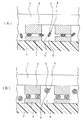
図1は、本発明による異方導電性接着剤を用いて、ベアICを回路基板に実装する工程を模式的に示す断面図である。
1は、バンプ電極2を設けたベアICを表す。このベアIC1を回路基板7に実装するには、図1(A)のように、ベアIC1と回路基板7との間に異方導電性接着剤を挟み、バンプ電極2とこれを接続する回路基板の電極3とが対応するように位置あわせをした上で、両者を機械的に加圧して接近させる。異方導電性接着剤は、偏平形状の粒子4が分散されている熱硬化性の絶縁性接着剤6からなる。前記粒子4は、直径20μmの球形の形状記憶樹脂粒子9の表面を導電性被膜5で被覆した後、40℃に加熱して力を加え偏平形状に変形させたものである。粒子4は、内部に空孔を有するため、比重が小さくなり、前記絶縁性接着剤6に均一に分散している。前記絶縁性接着剤6の硬化温度は、前記形状記憶樹脂粒子9が記憶する形状に復帰することができる温度よりも高い。
そして、図1(B)に示すように、100℃に加熱することによって、粒子4を元の球形に復帰させる。このとき前記粒子4が、前記両電極を押し広げながら復帰するので、両電極の電気的接続が完全なものとなる。そして、さらに130℃で加熱して絶縁性接着剤6を硬化させ、ベアIC1を回路基板7上に固定する。
【0015】
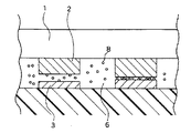
図2は、従来の異方導電性接着剤を用いて、回路基板上に電子部品を実装した断面図である。
ベアIC1と回路基板7が、導電性フィラー8を分散させた熱硬化性の絶縁性接着剤を間に挟んで設置され、機械的に加圧されて接近している。このとき、回路基板上に設置されたベアICを、どの場所でも同じ荷重がかかるように加圧することは難しい。そのため、回路基板7の電極3とベアIC1の電極2が、接近する場所と、離れる場所が生じる。両者が十分近くまで接近している場合は、導電性フィラー8が微細であっても、このフィラー8を介して両者を電気的に接続することができる。しかし、前記両者が離れている場合は、導電性フィラー8が両電極を接続することができない。そのため、回路基板7上に実装されたベアIC1は、電気的に接続される場所と、接続されない場所ができる。
【0016】
【実施例】
《実施例1》
図1と同様にして、異方導電性接着剤を作製した。ただし、形状記憶樹脂には、ポリウレタン系のものを用い、導電性被膜は金をメッキすることによって作成し、絶縁性接着剤は、エポキシ樹脂とイミダゾール系硬化剤からなるものを用いた。
そして、図1(A)に示すように、この異方導電性接着剤を回路基板7の電極3に塗布した後、数個のバンプ電極2を設けたベアIC1を回路基板7の電極1上に設置した。そして、ベアIC1と回路基板7を相互に機械的加圧した後、120℃で20秒間加熱して、図1(B)に示すように、粒子4をもとの球形に復帰させ、続いて130℃で30秒間加熱して、絶縁性接着剤6を硬化させた。
その結果、回路基板7上にベアIC1は固定され、その電気的接続は良好であった。
【0017】
【発明の効果】
上記のように、本発明によれば、種々の回路基板に、様々な電子部品を高性能に実装することができる。
【図面の簡単な説明】
【図1】本発明による異方導電性接着剤を用いて、ベアICを回路基板に実装する工程を模式的に示す断面図である。
【図2】従来の導電性フィラーを分散させた接着剤用いて、ベアICを回路基板に実装した図である。
【符号の説明】
1 ベアIC
2 バンプ電極
3 回路基板の電極
4 粒子
5 導電性被膜
6 絶縁性接着剤
7 回路基板
8 導電性フィラー
9 形状記憶樹脂粒子[0001]
BACKGROUND OF THE INVENTION
The present invention relates to an anisotropic conductive adhesive used when an electronic component such as a capacitor or a semiconductor chip is mounted on a circuit board with electrical connection, and a method for mounting the electronic component using the same.
[0002]
[Prior art]
In recent years, with the diversification of electronic components mounted on circuit boards, miniaturization of electronic parts and miniaturization of electrodes of circuit boards have progressed.
Conventionally, when mounting electronic components on a circuit board with electrical connection, anisotropic conductive adhesive in which conductive filler is dispersed in thermosetting insulating adhesive, or molded into sheet form Is used.
[0003]
In order to mount an electronic component such as a bare IC on a circuit board using such an adhesive, a bump electrode is provided on an electrode pad of the bare IC, and the bump electrode and the electrode of the circuit board are provided with the bump electrode. After the anisotropic conductive adhesive is installed, the both are mechanically pressurized with each other, so that the bump electrodes of the bare IC and the electrodes of the circuit board are electrically connected by the conductive filler dispersed in the adhesive. The approach is taken to be connected and then the insulating adhesive is cured. An activated carbon fiber or the like is used as the conductive filler.
In addition, a liquid material is more convenient than a sheet material because it can be freely applied to various shapes of substrates and various electronic components, and is widely used.
[0004]
[Problems to be solved by the invention]
However, in the conventional anisotropic conductive adhesive, the particle size of the conductive filler dispersed in the insulating adhesive is extremely small, and it is technically possible to perform mechanical pressurization uniformly over a wide area. Because of this, various problems have arisen.
First of all, it was difficult to set the joining conditions and the reproducibility was not good. Therefore, it has been difficult to mount many electronic components on the circuit board in good electrical connection.
Secondly, in order to complete the electrical connection, it is necessary to increase the load of mechanical pressurization, which causes distortion in the substrate and damage to the electronic components. There was an inconvenience.
[0005]
Third, activated carbon fibers that have been used as conductive fillers in the past are porous and therefore have high water absorption, resulting in unstable electrical connection between electronic components and circuit boards. It was.
Fourthly, since the conductive filler tends to settle in the insulating adhesive, it is difficult to use the conductive filler by uniformly dispersing it in the insulating adhesive.
In view of the above problems, the present invention provides an anisotropic conductive adhesive capable of stably mounting various electronic components on various circuit boards in an electrically good connection state, and an electronic component using the adhesive. It aims to provide a way to implement.
[0006]
[Means for Solving the Problems]
The anisotropic conductive adhesive according to the present invention comprises flat resin particles having a conductive film on the surface and a thermosetting insulating adhesive dispersed therein, and the resin particles are formed of the adhesive. When heated to a lower than the curing temperature temperature Ri Oh a shape memory resin particles to return to a spherical or similar shape, said shape-memory resin particles, characterized by having pores therein.
The electronic component mounting method according to the present invention includes a step of applying the adhesive to an electrode of an electronic component to be mounted or an electrode of a circuit board, a step of mechanically pressurizing and approaching the two, It comprises a step of heating and returning the shape memory resin particles to a memorized shape, and a step of further heating and curing the insulating adhesive to fix the component on the substrate.
[0007]
DETAILED DESCRIPTION OF THE INVENTION
Shape memory resin is a kind of thermoplastic elastomer and has a higher melting temperature of the hard phase than the soft phase and an appropriate temperature difference. When such a shape memory resin is molded by being heated to a temperature at which the hard phase is melted, unless it is heated again to a temperature at which the hard phase is melted, it continues to memorize the molded shape at this time. When heated to the melting temperature, it softens and can be deformed forcibly by applying external force.
When the temperature is lowered in the state of being deformed in this way, the soft phase is solidified, so that a resin that retains the deformed shape can be obtained. However, the hard phase of this resin retains its shape before deformation, so if the resin is softened again by heating to a temperature at which the soft phase melts in a state where external force is removed, the resin will deform. It will return to the previous shape. By utilizing such characteristics, the shape can be stored in the resin.
The shape memory resin particles used for the anisotropic conductive adhesive of the present invention are those using a resin having the above-described characteristics, and it is preferable to use a shape memory resin made of a polyurethane-based or norbornene-based material.
[0008]
The shape memory resin particles are in direct contact with both electrodes by restoring the shape while expanding the gap between the electrodes of the electronic component and the circuit board electrodes, which form a slight gap, and electrically connect the electrodes. Therefore, the shape memory resin particles are preliminarily molded into a spherical shape or a similar shape, memorized in this shape, and then heated to apply force and deformed into a flat shape. Use.
Further, at this time, in order to complete the electrical connection between both electrodes, it is preferable that the particle diameter when the shape memory resin particles return to the shape is 10 to 20 μm.
[0009]
In order to produce the anisotropic conductive adhesive according to the present invention, first, the material as described above is suspension-polymerized to form spherical or similar shaped particles. Thereafter, a conductive film is formed on the surface of the particles. Then, a force is applied by heating to a temperature at which the soft phase melts, the particles are deformed into a flat shape, the shape is memorized, and particles having a conductive coating on the surface are obtained. Finally, the particles are dispersed in a thermosetting insulating adhesive to complete the anisotropic conductive adhesive.
The conductive film is preferably formed of a conductive material such as gold, tin, aluminum, nickel, or carbon by a method such as plating or vapor deposition.
The shape memory resin particles coated with a conductive coating in this way are not as water-absorbing as the activated carbon fibers that have been used as conventional conductive fillers, so the circuit board and electronic components can be connected stably over a long period of time. can do.
[0010]
When an electronic component is mounted on a circuit board using the anisotropic conductive adhesive according to the present invention, a step of curing the insulating adhesive is performed after returning the shape memory resin particles to a memorized shape. Therefore, the temperature at which the shape memory resin particles return to the shape memorized needs to be lower than the temperature at which the insulating adhesive is cured within a limited time in the mounting process. As the insulating adhesive for dispersing the shape memory resin particles made of the aforementioned materials, it is preferable to use an adhesive obtained by adding imidazoles as a curing agent to an epoxy resin, or an adhesive obtained by adding carboxylic acids to an oxazoline resin. is there.
[0011]
When the anisotropic conductive adhesive according to the present invention is used, for example, when a bare IC that is a semiconductor component is mounted on a circuit board, even if the pitch distance between bump electrodes provided on the bare IC is a narrow pitch of 50 μm or less. Good electrical connection can be made.
Further, by using the shape memory resin particles having a spherical shape or a shape similar to the spherical shape, both electrodes can be stably bonded, and the reproducibility of setting the bonding conditions is facilitated.
[0012]
To mount an electronic component using the anisotropic conductive adhesive as described above, the adhesive is applied to the electrode portion of the circuit board or the electrode portion of the electronic component to be mounted, and the both electrodes correspond to each other. After the alignment, the two electrodes are brought close to each other by mechanically pressurizing the circuit board and the electronic component. Thereafter, the shape of the shape memory resin particles is restored to the shape memorized by the step of heating the substrate, and the insulating adhesive is cured by heating at a higher temperature, and the electronic component is fixed on the circuit board.
[0013]
When the shape of the shape memory resin particles is restored, the shape of the shape memory resin particles cannot be restored if the insulating adhesive is first cured. Therefore, in the heating device for mounting electronic components, the temperature is first applied to the substrate to return to the shape memorized by the shape memory resin particles, and the device is controlled so that the higher temperature is applied and the insulating adhesive is cured. To do.
As described above, since the shape memory resin particles return to the shape memorized and the electrodes are electrically connected completely, there is no need to increase the mechanical pressure as in the prior art. Therefore, there is no inconvenience of causing distortion or the like in the circuit board or the electronic component.
[0014]
Hereinafter, the present invention will be described in more detail with reference to specific examples and drawings.
FIG. 1 is a cross-sectional view schematically showing a process of mounting a bare IC on a circuit board using the anisotropic conductive adhesive according to the present invention.
Reference numeral 1 denotes a bare IC provided with a bump electrode 2. In order to mount the bare IC 1 on the circuit board 7, as shown in FIG. 1A, an anisotropic conductive adhesive is sandwiched between the bare IC 1 and the circuit board 7, and the bump electrode 2 is connected to the circuit. After alignment so that the
And as shown to FIG. 1 (B), the particle | grains 4 are returned to the original spherical form by heating to 100 degreeC. At this time, the particles 4 return while spreading both electrodes, so that the electrical connection between both electrodes becomes complete. Further, the insulating adhesive 6 is cured by heating at 130 ° C., and the bare IC 1 is fixed on the circuit board 7.
[0015]
FIG. 2 is a cross-sectional view in which an electronic component is mounted on a circuit board using a conventional anisotropic conductive adhesive.
The bare IC 1 and the circuit board 7 are placed with a thermosetting insulating adhesive in which the conductive filler 8 is dispersed interposed therebetween, and are mechanically pressurized and approached. At this time, it is difficult to pressurize the bare IC installed on the circuit board so that the same load is applied at any place. For this reason, there are places where the
[0016]
【Example】
Example 1
An anisotropic conductive adhesive was produced in the same manner as in FIG. However, the shape memory resin is a polyurethane-based one, the conductive coating is prepared by plating gold, and the insulating adhesive is an epoxy resin and an imidazole-based curing agent.
Then, as shown in FIG. 1A, after applying this anisotropic conductive adhesive to the
As a result, the bare IC 1 was fixed on the circuit board 7, and the electrical connection was good.
[0017]
【The invention's effect】
As described above, according to the present invention, various electronic components can be mounted on various circuit boards with high performance.
[Brief description of the drawings]
FIG. 1 is a cross-sectional view schematically showing a process of mounting a bare IC on a circuit board using an anisotropic conductive adhesive according to the present invention.
FIG. 2 is a diagram in which a bare IC is mounted on a circuit board using an adhesive in which a conventional conductive filler is dispersed.
[Explanation of symbols]
1 Bear IC
2 Bump
Claims (4)
Priority Applications (1)
| Application Number | Priority Date | Filing Date | Title |
|---|---|---|---|
| JP103698A JP4040734B2 (en) | 1998-01-06 | 1998-01-06 | Anisotropic conductive adhesive and electronic component mounting method using the same |
Applications Claiming Priority (1)
| Application Number | Priority Date | Filing Date | Title |
|---|---|---|---|
| JP103698A JP4040734B2 (en) | 1998-01-06 | 1998-01-06 | Anisotropic conductive adhesive and electronic component mounting method using the same |
Publications (2)
| Publication Number | Publication Date |
|---|---|
| JPH11199843A JPH11199843A (en) | 1999-07-27 |
| JP4040734B2 true JP4040734B2 (en) | 2008-01-30 |
Family
ID=11490347
Family Applications (1)
| Application Number | Title | Priority Date | Filing Date |
|---|---|---|---|
| JP103698A Expired - Fee Related JP4040734B2 (en) | 1998-01-06 | 1998-01-06 | Anisotropic conductive adhesive and electronic component mounting method using the same |
Country Status (1)
| Country | Link |
|---|---|
| JP (1) | JP4040734B2 (en) |
Families Citing this family (1)
| Publication number | Priority date | Publication date | Assignee | Title |
|---|---|---|---|---|
| JP4591138B2 (en) * | 2005-03-15 | 2010-12-01 | パナソニック株式会社 | Conductive composition and wiring board |
-
1998
- 1998-01-06 JP JP103698A patent/JP4040734B2/en not_active Expired - Fee Related
Also Published As
| Publication number | Publication date |
|---|---|
| JPH11199843A (en) | 1999-07-27 |
Similar Documents
| Publication | Publication Date | Title |
|---|---|---|
| KR100382759B1 (en) | Method of packaging semiconductor device using anisotropic conductive adhesive | |
| US5749997A (en) | Composite bump tape automated bonding method and bonded structure | |
| JP4123998B2 (en) | Electronic circuit device and manufacturing method thereof | |
| JP2001052778A (en) | Anisotropic conductive adhesive film and method for producing the same | |
| JP3801666B2 (en) | Electrode connection method and connection member used therefor | |
| KR100563890B1 (en) | Electrical connecting device and electrical connecting method | |
| KR19990044151A (en) | Strongly bonded substrate assembly for deformable electronics | |
| KR100701133B1 (en) | Electrical connection device and electrical connection method | |
| JP4040734B2 (en) | Anisotropic conductive adhesive and electronic component mounting method using the same | |
| JPH08148211A (en) | Connection member and structure and method for connecting electrode using the same | |
| JPS63151033A (en) | Manufacture of semiconductor device | |
| JPH11103158A (en) | Flip chip mounting method and mounting structure on printed wiring board | |
| JP2710234B2 (en) | Terminal connection method and circuit board manufactured by this method | |
| JP3162068B2 (en) | Semiconductor chip mounting method | |
| JP3745524B2 (en) | Anisotropic conductive adhesive sheet and electronic component mounting method using the same | |
| JPH087658A (en) | Anisotropic conductive adhesive film | |
| JPS60225828A (en) | How to mount the LCD panel | |
| JP2937705B2 (en) | Connection method of printed wiring board | |
| JP4378788B2 (en) | IC chip connection method | |
| US6194780B1 (en) | Tape automated bonding method and bonded structure | |
| JP2000174066A (en) | Semiconductor device mounting method | |
| JP4155470B2 (en) | Electrode connection method using connecting members | |
| KR980013552A (en) | A connection sheet for mutually connecting the electrodes facing each other, and an electrode connection structure and a connection method using the connection sheet | |
| JPH08102464A (en) | Projection electrode structure and method of forming the same, connection structure using the projection electrode and method of connecting the same | |
| JP2940252B2 (en) | Semiconductor device mounting structure and mounting method |
Legal Events
| Date | Code | Title | Description |
|---|---|---|---|
| A621 | Written request for application examination |
Free format text: JAPANESE INTERMEDIATE CODE: A621 Effective date: 20050105 |
|
| A977 | Report on retrieval |
Free format text: JAPANESE INTERMEDIATE CODE: A971007 Effective date: 20070717 |
|
| A131 | Notification of reasons for refusal |
Effective date: 20070719 Free format text: JAPANESE INTERMEDIATE CODE: A131 |
|
| A521 | Written amendment |
Effective date: 20070914 Free format text: JAPANESE INTERMEDIATE CODE: A523 |
|
| TRDD | Decision of grant or rejection written | ||
| A01 | Written decision to grant a patent or to grant a registration (utility model) |
Free format text: JAPANESE INTERMEDIATE CODE: A01 Effective date: 20071011 |
|
| A61 | First payment of annual fees (during grant procedure) |
Free format text: JAPANESE INTERMEDIATE CODE: A61 Effective date: 20071108 |
|
| FPAY | Renewal fee payment (prs date is renewal date of database) |
Year of fee payment: 3 Free format text: PAYMENT UNTIL: 20101116 |
|
| R150 | Certificate of patent (=grant) or registration of utility model |
Free format text: JAPANESE INTERMEDIATE CODE: R150 |
|
| FPAY | Renewal fee payment (prs date is renewal date of database) |
Free format text: PAYMENT UNTIL: 20111116 Year of fee payment: 4 |
|
| FPAY | Renewal fee payment (prs date is renewal date of database) |
Free format text: PAYMENT UNTIL: 20121116 Year of fee payment: 5 |
|
| LAPS | Cancellation because of no payment of annual fees |