JP4034781B2 - Clock generator for integrated circuits - Google Patents
Clock generator for integrated circuits Download PDFInfo
- Publication number
- JP4034781B2 JP4034781B2 JP2004530065A JP2004530065A JP4034781B2 JP 4034781 B2 JP4034781 B2 JP 4034781B2 JP 2004530065 A JP2004530065 A JP 2004530065A JP 2004530065 A JP2004530065 A JP 2004530065A JP 4034781 B2 JP4034781 B2 JP 4034781B2
- Authority
- JP
- Japan
- Prior art keywords
- clock
- clock generator
- current source
- node
- generator
- Prior art date
- Legal status (The legal status is an assumption and is not a legal conclusion. Google has not performed a legal analysis and makes no representation as to the accuracy of the status listed.)
- Expired - Lifetime
Links
Images


Classifications
-
- G—PHYSICS
- G06—COMPUTING; CALCULATING OR COUNTING
- G06F—ELECTRIC DIGITAL DATA PROCESSING
- G06F1/00—Details not covered by groups G06F3/00 - G06F13/00 and G06F21/00
- G06F1/04—Generating or distributing clock signals or signals derived directly therefrom
-
- H—ELECTRICITY
- H03—ELECTRONIC CIRCUITRY
- H03B—GENERATION OF OSCILLATIONS, DIRECTLY OR BY FREQUENCY-CHANGING, BY CIRCUITS EMPLOYING ACTIVE ELEMENTS WHICH OPERATE IN A NON-SWITCHING MANNER; GENERATION OF NOISE BY SUCH CIRCUITS
- H03B5/00—Generation of oscillations using amplifier with regenerative feedback from output to input
- H03B5/08—Generation of oscillations using amplifier with regenerative feedback from output to input with frequency-determining element comprising lumped inductance and capacitance
- H03B5/12—Generation of oscillations using amplifier with regenerative feedback from output to input with frequency-determining element comprising lumped inductance and capacitance active element in amplifier being semiconductor device
- H03B5/1206—Generation of oscillations using amplifier with regenerative feedback from output to input with frequency-determining element comprising lumped inductance and capacitance active element in amplifier being semiconductor device using multiple transistors for amplification
- H03B5/1212—Generation of oscillations using amplifier with regenerative feedback from output to input with frequency-determining element comprising lumped inductance and capacitance active element in amplifier being semiconductor device using multiple transistors for amplification the amplifier comprising a pair of transistors, wherein an output terminal of each being connected to an input terminal of the other, e.g. a cross coupled pair
-
- G—PHYSICS
- G06—COMPUTING; CALCULATING OR COUNTING
- G06F—ELECTRIC DIGITAL DATA PROCESSING
- G06F1/00—Details not covered by groups G06F3/00 - G06F13/00 and G06F21/00
- G06F1/04—Generating or distributing clock signals or signals derived directly therefrom
- G06F1/08—Clock generators with changeable or programmable clock frequency
-
- H—ELECTRICITY
- H03—ELECTRONIC CIRCUITRY
- H03B—GENERATION OF OSCILLATIONS, DIRECTLY OR BY FREQUENCY-CHANGING, BY CIRCUITS EMPLOYING ACTIVE ELEMENTS WHICH OPERATE IN A NON-SWITCHING MANNER; GENERATION OF NOISE BY SUCH CIRCUITS
- H03B5/00—Generation of oscillations using amplifier with regenerative feedback from output to input
- H03B5/08—Generation of oscillations using amplifier with regenerative feedback from output to input with frequency-determining element comprising lumped inductance and capacitance
- H03B5/12—Generation of oscillations using amplifier with regenerative feedback from output to input with frequency-determining element comprising lumped inductance and capacitance active element in amplifier being semiconductor device
- H03B5/1228—Generation of oscillations using amplifier with regenerative feedback from output to input with frequency-determining element comprising lumped inductance and capacitance active element in amplifier being semiconductor device the amplifier comprising one or more field effect transistors
-
- H—ELECTRICITY
- H03—ELECTRONIC CIRCUITRY
- H03K—PULSE TECHNIQUE
- H03K3/00—Circuits for generating electric pulses; Monostable, bistable or multistable circuits
- H03K3/02—Generators characterised by the type of circuit or by the means used for producing pulses
- H03K3/353—Generators characterised by the type of circuit or by the means used for producing pulses by the use, as active elements, of field-effect transistors with internal or external positive feedback
- H03K3/354—Astable circuits
Abstract
Description
本発明は、一般に電子デバイスの分野に関し、より詳細には、システム上にあるクロック駆動されるロジックのキャパシタンスに基づく振動信号を生成するデータ処理システム用のクロック・ジェネレータ回路の設計に関する。 The present invention relates generally to the field of electronic devices, and more particularly to the design of a clock generator circuit for a data processing system that generates a vibration signal based on the capacitance of clocked logic on the system.
電子テバイスの分野では、クロック信号およびクロック・ジェネレータ回路は周知である。従来のクロック・ジェネレータは、大まかに2種類に分けることができる。すなわち、汎用のマイクロプロセッサやデジタル信号プロセッサなどのVLSIデバイス用のジェネレータと、携帯電話などの消費者向け電子機器用のジェネレータである。図1を参照すると、VLSI用ジェネレータ104がVLSIデバイス101の一部分として示されている。VLSIデバイス101は、シリコン基板などのモノリシック基板上に製作された単一のデバイスを含む。デバイス101は、クロック・ジェネレータ回路104と、バッファ回路106と、まとめて負荷110として示す機能ロジックとを含む。VLSIデバイス101は、通常、水晶などの外部クロック・デバイス102から入力を受け取る。デバイス101は、オンチップ・クロックにおける周波数または位相あるいはその両方の変化を最小限にするための位相ロック・ループまたは遅延ロック・ループなど、何らかの形のクロック発生回路104を含む。次いでクロック・ジェネレータ104の出力は、通常、バッファ回路106によって増幅またはバッファリングされる。バッファ回路106の出力は、デバイス101の機能ロジック(負荷110)を駆動する。
In the field of electronic devices, clock signals and clock generator circuits are well known. Conventional clock generators can be roughly divided into two types. That is, a generator for VLSI devices such as general-purpose microprocessors and digital signal processors, and a generator for consumer electronic devices such as mobile phones. Referring to FIG. 1, a
図2を参照すると、指数ホーン形のバッファ回路106の実装形態が示されている。この図では、バッファ回路106は、一連の従来型CMOSインバータ120を含む。連続する各インバータのサイズ(トランジスタの幅と長さの比(W/L)として測定した)は、ある公比で前のインバータのサイズよりも大きくなっている。
Referring to FIG. 2, an implementation of an exponent
歴史的には、負荷110に加えられるクロック信号の周波数は、数十から数百メガヘルツの範囲内であった。このような周波数では、負荷110に関連する浮遊キャパシタンスはクロック信号の形状を大きく変化させるには十分でなく、したがってクロック信号はほぼ正方形である。方形波信号は、一般に、CMOSデバイスのクロック信号として望ましい。それは、この種の信号はすばやく状態間で遷移するので、CMOSのクロスオーバ電流が減少し、閾値電圧でのデバイス内部の変化に関連する問題が最小限になり有益であるからである。
Historically, the frequency of the clock signal applied to the
しかし回路が進歩するにつれて、方形波クロック信号の生成はますます問題となってきた。良好な方形波の生成に必要な高周波成分は、どんな半導体デバイスにも伴う浮遊キャパシタンスによって大幅に減衰される。製造業者達は、概して、浮遊キャパシタンスを減少させることよりもクロック周波数を増加させることに成功しており、その結果、方形波を生成することがますます難しくなっている。この問題のため、設計者達は、方形波と比べて比較的遅い立ち上がり時間および立ち下り時間を有するクロック信号の効果について考えるようになった。 However, as circuits have advanced, the generation of square wave clock signals has become increasingly problematic. The high frequency components necessary to produce a good square wave are greatly attenuated by the stray capacitance associated with any semiconductor device. Manufacturers have generally succeeded in increasing the clock frequency rather than reducing stray capacitance, and as a result, it is increasingly difficult to generate a square wave. Because of this problem, designers have come to consider the effect of clock signals having relatively slow rise and fall times compared to square waves.
一方、家電用回路には、一般に、より単純で低コストのクロック・ジェネレータが実装されてきた。最も一般的には、LとCの組み合わせによってほぼ正弦波の信号を生成する何らかの形のタンク回路がこれらの回路に組み込まれる。この信号は、バッファリングされ、デバイスの機能回路に供給される。 On the other hand, generally simpler and lower-cost clock generators have been mounted on home appliance circuits. Most commonly, some form of tank circuit is built into these circuits that generates a nearly sinusoidal signal by the combination of L and C. This signal is buffered and supplied to the functional circuit of the device.
VLSI用クロック・ジェネレータは一般に、品質および同調レンジの点で家電の信号ジェネレータよりも優れているが、外部クロック信号を必要とし、望ましくない電力量をバッファ回路内で消費する傾向がある。消費製品のクロック回路は安価であるという長所があるが、立ち上がり時間が遅く、従来のクロック周波数で充分なサイズのインダクタおよびコンデンサを設計することは非現実的であるので、一般にVLSIデバイスには不適当であった。(LC回路の特性周波数は、LとCの積の平方根に反比例する)。 VLSI clock generators are generally superior to home appliance signal generators in terms of quality and tuning range, but require an external clock signal and tend to consume an undesirable amount of power in the buffer circuit. Although the clock circuit of a consumer product has the advantage of being inexpensive, it is generally impractical for VLSI devices because it has a slow rise time and it is impractical to design inductors and capacitors of sufficient size at conventional clock frequencies. It was appropriate. (The characteristic frequency of the LC circuit is inversely proportional to the square root of the product of L and C).
クロック信号の質に対して過度に妥協することなく、且つ非現実的なダイ・サイズになることのない、消費製品のクロック・ジェネレータの長所を組み込んだVLSIデバイス用のクロック発生回路を実装することが望ましい。 Implement a clock generation circuit for VLSI devices that incorporates the advantages of a consumer clock generator without overcompromising the quality of the clock signal and without unrealistic die size. Is desirable.
上で特定した問題は、電流源と反転スイッチの間にオンチップ誘導要素が接続されたクロック・ジェネレータを含むシステムおよび集積回路(ダイ)によって主に対処される。スイッチの出力は、クロック駆動される回路の少なくとも一部分を中間のバッファリングなしに駆動やクロックするのに適したほぼ正弦波の信号である。好ましい実施形態では、クロック・ジェネレータは、1対のクロス・カップル型MOSFET、1対のソリッド・ステート・オンチップ・インダクタ、および電流源を含むデュアル位相設計である。各オンチップ・インダクタは、電流源と一方のMOSFETのドレインとの間に接続される。クロック・ジェネレータの出力は、ダイ上にあるクロック駆動される回路の少なくとも一部分のクロック入力部に直接供給される。この実施形態では、クロック・ジェネレータの出力信号の周波数は、誘導要素のインダクタンスおよびクロック駆動される回路のキャパシタンスによってほぼ決まる。この設計は、クロック・ジェネレータ自体に別個のコンデンサ素子を組み込む必要性をなくし、電力の大部分をジェネレータの誘導要素と負荷の容量要素との間で往復させそれにより電流源が供給する必要のある電力が低減されたクロック・ジェネレータをもたらす。 The problems identified above are addressed primarily by systems and integrated circuits (dies) that include a clock generator with an on-chip inductive element connected between a current source and an inverting switch. The output of the switch is a generally sinusoidal signal suitable for driving and clocking at least a portion of the clocked circuit without intermediate buffering. In the preferred embodiment, the clock generator is a dual phase design that includes a pair of cross-coupled MOSFETs, a pair of solid state on-chip inductors, and a current source. Each on-chip inductor is connected between a current source and the drain of one MOSFET. The output of the clock generator is fed directly to the clock input of at least a portion of the clocked circuit on the die. In this embodiment, the frequency of the clock generator output signal is largely determined by the inductance of the inductive element and the capacitance of the clocked circuit. This design eliminates the need to incorporate a separate capacitor element in the clock generator itself, requiring most of the power to be shuttled between the generator inductive element and the load capacitive element, thereby providing a current source. This results in a clock generator with reduced power.
本発明の他の目的および長所は、以下の詳細な説明を読み、添付の図面を参照することによって明らかとなるであろう。 Other objects and advantages of the present invention will become apparent upon reading the following detailed description and upon reference to the accompanying drawings in which:
本発明には、様々な変更形態および代替形態が可能であるが、例として本発明の特定の実施形態を図面に示し、ここで詳細に説明することとする。しかし、本明細書に示す図面および詳細な説明は、ここに開示した特定の実施形態に本発明を限定するものではなく、反対に、添付の特許請求の範囲によって定義される本発明の趣旨および範囲内に含まれる修正物、等価物、および代替物をすべて含むことを意図していることが理解されるべきである。 While the invention is susceptible to various modifications and alternative forms, specific embodiments thereof are shown by way of example in the drawings and will herein be described in detail. However, the drawings and detailed description set forth herein are not intended to limit the invention to the specific embodiments disclosed herein, and, on the contrary, are within the spirit and scope of the invention as defined by the appended claims. It should be understood that all modifications, equivalents, and alternatives included within the scope are intended to be included.
一般的に言えば、本発明は、汎用のマイクロプロセッサまたはデジタル信号処理装置などのVLSIデバイス用のオンチップ・クロック・ジェネレータを含む、本明細書ではデバイスまたはダイとも呼ぶ集積回路を企図するものである。一実施形態では、クロック・ジェネレータ回路は少なくとも1個のソリッド・ステート・インダクタを含むが、従来のLCタンク回路に典型的なコンデンサ素子は省かれる。その代わりに、クロック・ジェネレータによって駆動される回路に固有のキャパシタンスがジェネレータの容量要素となる。別の実施形態では、固有のデバイス・キャパシタンスが、ジェネレータ回路の一部分を構成するディスクリート・コンデンサによって補足される。 Generally speaking, the present invention contemplates an integrated circuit, also referred to herein as a device or die, that includes an on-chip clock generator for VLSI devices such as general purpose microprocessors or digital signal processors. is there. In one embodiment, the clock generator circuit includes at least one solid state inductor, but the capacitor elements typical of conventional LC tank circuits are omitted. Instead, the capacitance inherent in the circuit driven by the clock generator becomes the capacitive element of the generator. In another embodiment, the inherent device capacitance is supplemented by a discrete capacitor that forms part of the generator circuit.
クロック・ジェネレータの出力部は、クロック駆動される回路のクロック入力部に直接接続される。この設計では、クロック・ジェネレータのインダクタとクロック駆動される回路の浮遊キャパシタンスとの間でエネルギーが往復する。従来のVLSIクロック・ジェネレータ内で大きなエネルギーを消費するバッファ回路は使用しない。 The output of the clock generator is directly connected to the clock input of the clock driven circuit. In this design, energy travels back and forth between the clock generator inductor and the stray capacitance of the clocked circuit. A buffer circuit that consumes large energy in the conventional VLSI clock generator is not used.
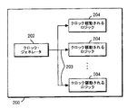
次に図面を参照すると、図3は、集積回路200の選択された要素のブロック図である。この図では、集積回路200が、オンチップ・クロック・ジェネレータ202と、参照番号204として示された1組のクロック駆動される回路またはロジックとを含むものとして示されている。クロック駆動されるロジック204は、ジェネレータ202によって生成されたクロック信号203を受け取り、またはその特性に影響を及ぼす集積回路200のロジック要素を表す。したがってクロック駆動されるロジック204は、クロックを使用する従来のフリップフロップなどの同期式ロジック要素およびドミノ・ロジック・ゲートなどの組み合わせゲートと、ジェネレータ202とロジック要素の間の相互接続部とを含む。本発明の好ましい実施形態では、クロック駆動されるロジック204は、図1に関して上述したバッファ回路106などのバッファ回路を含まない。換言すれば、集積回路200の一実施形態は、クロック・ジェネレータ202とクロック駆動されるロジック204との間を、バッファリングなしで直接接続することを企図している。電子工学および電子設計の分野の技術者には、クロック・ジェネレータ202の出力をロードされる浮遊キャパシタンスまたは固有キャパシタンスをクロック駆動されるロジック204の各要素を含むことが理解されるであろう。したがって本発明の観点から、図3では、集積回路200が主にクロック・ジェネレータおよびそれが駆動する容量性負荷から構成されることを強調して示してある。
Referring now to the drawings, FIG. 3 is a block diagram of selected elements of
本発明は一般に、容量性負荷を、クロック・ジェネレータの設計に組み込むことによって利用するものである。典型的には、本発明によるクロック・ジェネレータは修正されたタンク回路を備え、これによってクロック・ジェネレータ自体の中に設計で組み込まれた容量要素の必要性はなくなるまたは低減する。その代わりに、クロック・ジェネレータの出力ノードは、クロック駆動されるロジックに直接接続される。この構成では、ディスクリート・コンデンサに必要なスペースを割かずに、コンデンサを意図的にジェネレータ内に設計した場合にそのコンデンサが及ぼすのと同様に、容量性負荷が出力信号に影響を及ぼす。 The present invention generally utilizes a capacitive load by incorporating it into a clock generator design. Typically, a clock generator according to the present invention comprises a modified tank circuit, thereby eliminating or reducing the need for capacitive elements incorporated in the design within the clock generator itself. Instead, the output node of the clock generator is connected directly to the clocked logic. In this configuration, the capacitive load affects the output signal in the same way that the capacitor would have if it were intentionally designed in the generator without taking up the space required for the discrete capacitor.
次に図4を参照すると、本発明の一実施形態によるデュアル位相クロック・ジェネレータ回路202の実装形態が示されている。この実施形態では、クロック・ジェネレータ202は、1対のインダクタ212および214と、それに対応する1対のクロス・カップル型MOSFETデバイス216および218とを含む。MOSFETデバイス216および218はノード220上および222上にデュアル位相クロック信号を発生させる。そのクロック信号の位相は180度離れている。インダクタ212は、VCCに結合されているバイアスされたPMOSトランジスタ210の形をとる電流源とトランジスタ216のドレイン端子との間に接続される。インダクタ214は、電流源とトランジスタ218のドレイン端子との間に接続される。トランジスタ216のゲートおよびトランジスタ218のドレインは、クロック信号を供給するクロック・ジェネレータの出力ノード220に接続される。トランジスタ218のゲートおよびトランジスタ216のドレインは、クロック・バー信号を供給するクロック・ジェネレータの出力ノード222に接続される。出力ノード220および222は、クロック駆動されるロジック204に直接接続される。この図では、クロック駆動されるロジック204は、単にCloadのキャパシタンスを有するコンデンサとして表す。
Referring now to FIG. 4, an implementation of a dual phase
図4に示したように、クロック・ジェネレータ202は、クロック・ジェネレータの負荷によってキャパシタンスが提供されるLC回路として動作する。回路設計に詳しい者には、クロックおよびクロック・バー信号がほぼ正弦波であることが理解されるであろう。正方形の信号クロックは、スキュー時間がより短くまたクロスオーバ電流を減少させるので、正弦波よりも好ましいが、クロック周波数が増加してきたペースの方が、半導体製造業者達がデバイス内部の容量性ローディングを減少させることができたスピードよりも速かったので、従来のクロック・ジェネレータ回路でもほぼ正方形の信号を供給することがますますできなくなっている。クロック信号がますます「非正方形」になる現実に直面して、少々遅い立ち上がり時間および少々大きなクロスオーバ電流に対して耐性のある回路を設計することが、現在、回路設計者に求められている。したがって、クロック・ジェネレータ202によって生成される正弦波信号は、各種の最先端VLSIデバイスにとって十分であると理論付けられる。
As shown in FIG. 4, the
場合によっては、クロック駆動されるロジック204のCloadは、所望のクロック信号周波数にとって不十分である。他の場合では、Cloadは時間と共に変化することがある。これらの可能性を補償するために、図5に示すクロック・ジェネレータ202の一実施形態では、負荷キャパシタンスの補足または安定あるいはその両方を行う「設計に組み込んだ」コンデンサが組み込まれる。図5のデュアル位相クロック・ジェネレータ202の実装形態では、クロック・ジェネレータ202は、クロック・バー信号出力部とグラウンドとの間に接続された第1のコンデンサ230、ならびにクロック信号出力部とグラウンドとの間に接続された第2のコンデンサ232を含む。一実施形態では、コンデンサ230および232のキャパシタンスは制御可能に変更可能であり、ジェネレータが、コンデンサ230および232のキャパシタンスを変化させて負荷キャパシタンスCload内の変化を相殺し、それによって全体のキャパシタンスをほぼ一定に維持するように構成されている。
In some cases, the C load of the clocked
クロック・ジェネレータの出力ノード220および222を、クロック駆動されるロジック204に直接接続することによって、図1および図2に関して前述した指数ホーン形などのバッファ回路なしでジェネレータが実装される。集積回路200上の貴重な面積が節約されることに加え、バッファ回路の除去により、デバイス全体で必要な電力のかなりの部分を占めるクロック信号の生成に関連する電力消費量が、場合によっては劇的に減少するという有益な結果となる。従来のLC回路におけるこれまでのバッファリング(例えば、だんだんと大きくなる一連のCMOSインバータ)では、クロック・ジェネレータのエネルギー貯蔵要素から伝達されるエネルギーはすべてインバータのグラウンドに放散する。1サイクル毎に、クロック・ジェネレータはそれ自体を充電するのに十分な電流を引き込む必要がある。一方、図4に示すクロック・ジェネレータ202は、有益なことにエネルギーを「再循環」する。1クロック・サイクル毎に、インダクタ214の貯蔵されたエネルギーは、クロック駆動されるロジック204に伝達されて容量性負荷にロードされ、インダクタに戻される。したがって、LC回路が充電された後は、電流源210から必要な電流は、デバイス内の必然的に損失の多い要素を補償するのに必要な電流だけである。
By connecting the clock
さらに、VLSIデバイスがギガ・ヘルツ領域へと進歩するにつれ、LおよびCのサイズに関する要件は、十分に従来製法の製造能力の範囲内にあり過度に大きな面積を占めないインダクタ212および214の実装を可能にするのに十分なほど小さくなってきた。ナノ・ヘンリー範囲内にある、約5〜15のQを有するインダクタは、従来の多層メタルCMOSの製法で製造することができる。インダクタ212および214は、通常、何らかのループまたはスパイラルの形に作られる。図6を参照すると、インダクタ212および214の一実施形態の平面図が示されている。この実施形態では、金属でできた単一の層、通常は最上層の金属によってインダクタ対を実現する。多層インダクタ設計ではダイ面積の節約ができるものの、図6に示す単一層の実施形態の方が、通常、中間層からの漏出のある多層設計のものよりも優れたQ値を有している。さらに、図示したS字形の形状は、第1のインダクタ212によって誘起される磁場が第2のインダクタ214によって誘起される磁場と反対に作用し、それによって両方のインダクタのQ因子がさらに改善される構造を表している。
In addition, as VLSI devices have advanced to the gigahertz range, the L and C size requirements are well within the manufacturing capabilities of conventional manufacturing methods, and the implementation of
図4および図5で示す集積回路200の実施形態は、図7に示す等価回路の具体的な実装形態である。図7に示すように、本発明による集積回路200は、前記のオンチップ・インダクタを表す誘導要素Lと、クロック駆動される回路の固有キャパシタンスを含み、設計に組み込まれたコンデンサまたはディスクリート・コンデンサを含むことがある容量要素と、2つの抵抗要素Riおよび−Rpとを含む。Riは誘導要素Lの寄生抵抗を表し、負性抵抗−RpはRiでの寄生損失を補償するために追加された回路を表す。図4および図5に示す集積回路200の実施形態では、負性抵抗要素−Rpは、バイアスされたpチャネル電流源およびクロス・カップル型nチャネル・トランジスタを含む。代替実装形態では、例えばグラウンドとクロス・カップル型トランジスタ対との間に接続されたゲート・バイアスnチャネル電流源を含めることもできることが当業者には理解されよう。
The embodiment of the
本発明は、クロック信号を生成するのに適したエネルギー貯蔵要素として負荷キャパシタンスをソリッド・ステート・インダクタと併せて有益に使用するオンチップ・クロック・ジェネレータを有する集積回路を企図するものであることが、この開示の利益を有する技術分野の当業者には明らかであろう。詳細な説明および図面に示され記載された本発明の形態は、単に現時点での好ましい例とみなすべきことが理解されよう。添付の特許請求の範囲は、ここに開示した好ましい実施形態のすべての変形形態を包含するように広く解釈すべきことが意図されている。 The present invention contemplates an integrated circuit having an on-chip clock generator that advantageously uses load capacitance in combination with a solid state inductor as an energy storage element suitable for generating a clock signal. Will be apparent to those skilled in the art having the benefit of this disclosure. It will be understood that the form of the invention shown and described in the detailed description and drawings is merely to be regarded as a presently preferred example. It is intended that the appended claims be construed broadly to encompass all variations of the preferred embodiments disclosed herein.
Claims (5)
負荷キャパシタンスを有しクロック駆動される第2のVLSIロジック、及び
前記第1及び第2のVLSIロジックに提供されるクロック信号を生成するクロック・ジェネレータ回路であって、
電流源と、
前記電流源に、互いに並列に接続された第1のインダクタ及び第2のインダクタと、
前記第1のインダクタの前記電流源と反対側の端子(「第1ノード」とする)及び第2のインダクタの前記電流源と反対側の端子(「第2ノード」とする)に、夫々のドレインが接続された第1のNEFTと第2のNEFTであって、前記第1のNEFTのゲートは前記第2ノードに接続され、前記第2のNFETのゲートは前記第1ノードに接続されている、第1及び第2のNFETと、
を含む、クロック・ジェネレータ回路、
を含む集積回路デバイスにおいて、
前記第1ノードが前記第1のVLSIロジックに直接接続され、及び
前記第2ノードが前記第2のVLSIロジックに直接接続されている、
集積回路デバイス。A first VLSI logic having a load capacitance and clocked;
A second VLSI logic having a load capacitance and clocked; and a clock generator circuit for generating a clock signal provided to the first and second VLSI logic,
A current source;
A first inductor and a second inductor connected to the current source in parallel;
A terminal on the opposite side of the current source of the first inductor (referred to as “first node”) and a terminal on the opposite side of the current source of the second inductor (referred to as “second node”), respectively. A first NEFT and a second NEFT having drains connected, the gate of the first NEFT being connected to the second node, and the gate of the second NFET being connected to the first node; A first and second NFET;
Including a clock generator circuit,
In an integrated circuit device comprising:
The first node is directly connected to the first VLSI logic, and the second node is directly connected to the second VLSI logic;
Integrated circuit device.
Applications Claiming Priority (2)
| Application Number | Priority Date | Filing Date | Title |
|---|---|---|---|
| US10/216,618 US6650163B1 (en) | 2002-08-08 | 2002-08-08 | Clock generator for integrated circuit |
| PCT/EP2003/008486 WO2004019192A2 (en) | 2002-08-08 | 2003-07-10 | Clock generator for integrated circuit |
Publications (2)
| Publication Number | Publication Date |
|---|---|
| JP2005535265A JP2005535265A (en) | 2005-11-17 |
| JP4034781B2 true JP4034781B2 (en) | 2008-01-16 |
Family
ID=29420064
Family Applications (1)
| Application Number | Title | Priority Date | Filing Date |
|---|---|---|---|
| JP2004530065A Expired - Lifetime JP4034781B2 (en) | 2002-08-08 | 2003-07-10 | Clock generator for integrated circuits |
Country Status (9)
| Country | Link |
|---|---|
| US (1) | US6650163B1 (en) |
| EP (1) | EP1537467B1 (en) |
| JP (1) | JP4034781B2 (en) |
| KR (1) | KR20050083596A (en) |
| CN (1) | CN1316328C (en) |
| AT (1) | ATE384290T1 (en) |
| AU (1) | AU2003250200A1 (en) |
| DE (1) | DE60318724T2 (en) |
| WO (1) | WO2004019192A2 (en) |
Families Citing this family (15)
| Publication number | Priority date | Publication date | Assignee | Title |
|---|---|---|---|---|
| US7158596B2 (en) * | 2002-08-14 | 2007-01-02 | Standard Microsystems Corp. | Communication system and method for sending and receiving data at a higher or lower sample rate than a network frame rate using a phase locked loop |
| US7237217B2 (en) * | 2003-11-24 | 2007-06-26 | International Business Machines Corporation | Resonant tree driven clock distribution grid |
| US7202762B2 (en) * | 2004-06-09 | 2007-04-10 | Raytheon Company | Q enhancement circuit and method |
| US7126403B2 (en) * | 2004-11-01 | 2006-10-24 | Analog Devices, Inc. | LC tank clock driver with automatic tuning |
| JP4404756B2 (en) * | 2004-12-07 | 2010-01-27 | Okiセミコンダクタ株式会社 | Semiconductor integrated circuit |
| US7400169B2 (en) * | 2006-08-22 | 2008-07-15 | Broadcom Corporation | Inductor-tuned buffer circuit with improved modeling and design |
| US7906995B2 (en) * | 2009-02-26 | 2011-03-15 | Texas Instruments Incorporated | Clock buffer |
| US8710936B2 (en) | 2009-08-05 | 2014-04-29 | Apple Inc. | Resonant oscillator with start up and shut down circuitry |
| US8085103B2 (en) * | 2009-08-05 | 2011-12-27 | Apple Inc. | Resonant oscillator circuit with reduced startup transients |
| US8933665B2 (en) | 2009-08-05 | 2015-01-13 | Apple Inc. | Balancing voltages between battery banks |
| US8541999B2 (en) * | 2009-08-05 | 2013-09-24 | Apple Inc. | Controlling power loss in a switched-capacitor power converter |
| US8320141B2 (en) * | 2009-08-05 | 2012-11-27 | Apple Inc. | High-efficiency, switched-capacitor power conversion using a resonant clocking circuit to produce gate drive signals for switching capacitors |
| JP2011199590A (en) * | 2010-03-19 | 2011-10-06 | Fujitsu Ltd | Multiphase clock generating circuit |
| DE102020130542A1 (en) * | 2020-01-17 | 2021-07-22 | Taiwan Semiconductor Manufacturing Co., Ltd. | CLOCK CONTROL AND PROCEDURES FOR ITS OPERATION |
| CN114997087B (en) * | 2022-08-03 | 2022-10-25 | 飞腾信息技术有限公司 | Clock tree optimization method, optimization device and related equipment |
Family Cites Families (10)
| Publication number | Priority date | Publication date | Assignee | Title |
|---|---|---|---|---|
| US5559478A (en) * | 1995-07-17 | 1996-09-24 | University Of Southern California | Highly efficient, complementary, resonant pulse generation |
| DE19548629C1 (en) * | 1995-12-23 | 1997-07-24 | Itt Ind Gmbh Deutsche | Complementary clock system |
| US5920235A (en) * | 1997-06-25 | 1999-07-06 | Northern Telecom Limited | Voltage controlled oscillator integrated circuit |
| US6462623B1 (en) * | 1999-05-19 | 2002-10-08 | Parthus Ireland Limited | Method and apparatus for PLL with improved jitter performance |
| WO2001020784A1 (en) * | 1999-09-15 | 2001-03-22 | Thomson Licensing S.A. | Multi-clock integrated circuit with clock generator and bi-directional clock pin arrangement |
| US7555263B1 (en) * | 1999-10-21 | 2009-06-30 | Broadcom Corporation | Adaptive radio transceiver |
| US6340899B1 (en) * | 2000-02-24 | 2002-01-22 | Broadcom Corporation | Current-controlled CMOS circuits with inductive broadbanding |
| US6396316B1 (en) * | 2000-09-21 | 2002-05-28 | Sun Microsystems, Inc. | Clock buffer with LC circuit for jitter reduction |
| US6437653B1 (en) * | 2000-09-28 | 2002-08-20 | Sun Microsystems, Inc. | Method and apparatus for providing a variable inductor on a semiconductor chip |
| US6469587B2 (en) * | 2000-12-04 | 2002-10-22 | Agere Systems Guardian Corp. | Differential LC voltage-controlled oscillator |
-
2002
- 2002-08-08 US US10/216,618 patent/US6650163B1/en not_active Expired - Lifetime
-
2003
- 2003-07-10 KR KR1020057000415A patent/KR20050083596A/en not_active Application Discontinuation
- 2003-07-10 DE DE60318724T patent/DE60318724T2/en not_active Expired - Lifetime
- 2003-07-10 WO PCT/EP2003/008486 patent/WO2004019192A2/en active IP Right Grant
- 2003-07-10 CN CNB038188333A patent/CN1316328C/en not_active Expired - Lifetime
- 2003-07-10 AU AU2003250200A patent/AU2003250200A1/en not_active Abandoned
- 2003-07-10 JP JP2004530065A patent/JP4034781B2/en not_active Expired - Lifetime
- 2003-07-10 EP EP03792239A patent/EP1537467B1/en not_active Expired - Lifetime
- 2003-07-10 AT AT03792239T patent/ATE384290T1/en not_active IP Right Cessation
Also Published As
| Publication number | Publication date |
|---|---|
| CN1316328C (en) | 2007-05-16 |
| AU2003250200A1 (en) | 2004-03-11 |
| AU2003250200A8 (en) | 2004-03-11 |
| DE60318724T2 (en) | 2009-01-02 |
| EP1537467A2 (en) | 2005-06-08 |
| WO2004019192A3 (en) | 2004-09-10 |
| EP1537467B1 (en) | 2008-01-16 |
| WO2004019192A2 (en) | 2004-03-04 |
| JP2005535265A (en) | 2005-11-17 |
| ATE384290T1 (en) | 2008-02-15 |
| KR20050083596A (en) | 2005-08-26 |
| US6650163B1 (en) | 2003-11-18 |
| DE60318724D1 (en) | 2008-03-06 |
| CN1675610A (en) | 2005-09-28 |
Similar Documents
| Publication | Publication Date | Title |
|---|---|---|
| JP4034781B2 (en) | Clock generator for integrated circuits | |
| US7948263B2 (en) | Power gating circuit and integrated circuit including same | |
| US9058130B2 (en) | Tunable sector buffer for wide bandwidth resonant global clock distribution | |
| US8704576B1 (en) | Variable resistance switch for wide bandwidth resonant global clock distribution | |
| Chung et al. | A comparative analysis of low-power low-voltage dual-edge-triggered flip-flops | |
| US20050237096A1 (en) | Flipflop | |
| CN114567297B (en) | D-flip-flop, processor and computing device including the same | |
| CN210490799U (en) | SoC built-in oscillating circuit | |
| ur Rahman et al. | Quasi-resonant clocking: Continuous voltage-frequency scalable resonant clocking system for dynamic voltage-frequency scaling systems | |
| Jayaram et al. | A 10-MHz CMOS-based Ring Oscillator with Low Power consumption For On-chip IC Applications | |
| US9054682B2 (en) | Wide bandwidth resonant global clock distribution | |
| Sung et al. | A novel CMOS double-edge triggered flip-flop for low-power applications | |
| WO2001056084A1 (en) | Low power dissipation mos jam latch | |
| US8742817B2 (en) | Controlling impedance of a switch using high impedance voltage sources to provide more efficient clocking | |
| Lee et al. | A true single-phase clocked flip-flop with leakage current compensation | |
| Islam et al. | A low power dynamic logic with nmos based resistive keeper circuit | |
| CN114567292B (en) | Static latch and processor and computing device including same | |
| US10418939B2 (en) | LC resonant clock resource minimization using compensation capacitance | |
| Pedram et al. | Analysis of power-clocked CMOS with application to the design of energy-recovery circuits | |
| US11757406B2 (en) | Oscillator circuit | |
| Jung et al. | Design of a temperature-insensitive digitally-controlled oscillator for on-chip reference clock | |
| JPH1197627A (en) | Semiconductor integrated circuit and electronic device using the same | |
| Dabas et al. | A low power varactor based digitally controlled oscillator design in 180 nm CMOS technology | |
| Challagundla | Power and Skew Reduction Using Resonance Energy Recycling in FinFET based Wideband Clock Networks | |
| Mazumdar et al. | Design and physical implementation of a low frequency on-chip oscillator |
Legal Events
| Date | Code | Title | Description |
|---|---|---|---|
| A621 | Written request for application examination |
Free format text: JAPANESE INTERMEDIATE CODE: A621 Effective date: 20050405 |
|
| A977 | Report on retrieval |
Free format text: JAPANESE INTERMEDIATE CODE: A971007 Effective date: 20061117 |
|
| A131 | Notification of reasons for refusal |
Free format text: JAPANESE INTERMEDIATE CODE: A131 Effective date: 20061212 |
|
| A521 | Request for written amendment filed |
Free format text: JAPANESE INTERMEDIATE CODE: A821 Effective date: 20070309 Free format text: JAPANESE INTERMEDIATE CODE: A523 Effective date: 20070309 |
|
| RD12 | Notification of acceptance of power of sub attorney |
Free format text: JAPANESE INTERMEDIATE CODE: A7432 Effective date: 20070309 |
|
| A521 | Request for written amendment filed |
Free format text: JAPANESE INTERMEDIATE CODE: A821 Effective date: 20070312 |
|
| A02 | Decision of refusal |
Free format text: JAPANESE INTERMEDIATE CODE: A02 Effective date: 20070607 |
|
| A521 | Request for written amendment filed |
Free format text: JAPANESE INTERMEDIATE CODE: A821 Effective date: 20070821 Free format text: JAPANESE INTERMEDIATE CODE: A523 Effective date: 20070821 |
|
| A911 | Transfer to examiner for re-examination before appeal (zenchi) |
Free format text: JAPANESE INTERMEDIATE CODE: A911 Effective date: 20070927 |
|
| TRDD | Decision of grant or rejection written | ||
| A01 | Written decision to grant a patent or to grant a registration (utility model) |
Free format text: JAPANESE INTERMEDIATE CODE: A01 Effective date: 20071018 |
|
| A521 | Request for written amendment filed |
Free format text: JAPANESE INTERMEDIATE CODE: A821 Effective date: 20071018 |
|
| RD14 | Notification of resignation of power of sub attorney |
Free format text: JAPANESE INTERMEDIATE CODE: A7434 Effective date: 20071018 |
|
| A61 | First payment of annual fees (during grant procedure) |
Free format text: JAPANESE INTERMEDIATE CODE: A61 Effective date: 20071025 |
|
| FPAY | Renewal fee payment (event date is renewal date of database) |
Free format text: PAYMENT UNTIL: 20101102 Year of fee payment: 3 |
|
| R150 | Certificate of patent or registration of utility model |
Ref document number: 4034781 Country of ref document: JP Free format text: JAPANESE INTERMEDIATE CODE: R150 Free format text: JAPANESE INTERMEDIATE CODE: R150 |
|
| FPAY | Renewal fee payment (event date is renewal date of database) |
Free format text: PAYMENT UNTIL: 20111102 Year of fee payment: 4 |
|
| FPAY | Renewal fee payment (event date is renewal date of database) |
Free format text: PAYMENT UNTIL: 20121102 Year of fee payment: 5 |
|
| FPAY | Renewal fee payment (event date is renewal date of database) |
Free format text: PAYMENT UNTIL: 20121102 Year of fee payment: 5 |
|
| FPAY | Renewal fee payment (event date is renewal date of database) |
Free format text: PAYMENT UNTIL: 20131102 Year of fee payment: 6 |
|
| EXPY | Cancellation because of completion of term |