JP4033730B2 - Substrate mounting table for plasma processing apparatus, plasma processing apparatus, and base for plasma processing apparatus - Google Patents
Substrate mounting table for plasma processing apparatus, plasma processing apparatus, and base for plasma processing apparatus Download PDFInfo
- Publication number
- JP4033730B2 JP4033730B2 JP2002202000A JP2002202000A JP4033730B2 JP 4033730 B2 JP4033730 B2 JP 4033730B2 JP 2002202000 A JP2002202000 A JP 2002202000A JP 2002202000 A JP2002202000 A JP 2002202000A JP 4033730 B2 JP4033730 B2 JP 4033730B2
- Authority
- JP
- Japan
- Prior art keywords
- plasma processing
- processing apparatus
- mounting table
- substrate mounting
- electrostatic chuck
- Prior art date
- Legal status (The legal status is an assumption and is not a legal conclusion. Google has not performed a legal analysis and makes no representation as to the accuracy of the status listed.)
- Expired - Fee Related
Links
Images
Description
【0001】
【発明の属する技術分野】
本発明は、プラズマ処理装置用基板載置台及びプラズマ処理装置及びプラズマ処理装置用の基台部に係り、特に、プラズマを生起し、このプラズマを利用して半導体ウエハ等の被処理基板のエッチング処理、成膜処理等を行うプラズマ処理装置用基板載置台及びプラズマ処理装置及びプラズマ処理装置用の基台部に関する。
【0002】
【従来の技術】
従来から、プラズマを生起し、このプラズマを被処理物に作用させて所定の処理を施すプラズマ処理装置が多用されている。
【0003】
例えば、半導体装置の製造分野においては、半導体装置の微細な回路構造を形成する際に、半導体ウエハ等の被処理基板にプラズマを作用させて、エッチング処理や成膜処理等を行っている。
【0004】
このようなプラズマ処理装置では、減圧雰囲気とした真空チャンバ内のプラズマ処理室に被処理基板を配置してプラズマ処理を行うことから、真空チャックによって被処理基板を吸着保持することが困難であり、このため、被処理基板を吸着保持するための機構として静電チャックを用いたものが多い。なお、静電チャックは、セラミックス等の絶縁性部材の間に、タングステン等からなる静電チャック用電極を配設して構成されており、この静電チャック用電極に直流電圧を印加してクーロン力等により被処理基板を吸着保持するよう構成されている。
【0005】
また、所謂平行平板型のプラズマ処理装置では、被処理基板が載置される基板載置台が下部電極を兼ねることから、この基板載置台の基本的構成部分(基台部)は、アルミニウム等の導電性の金属等で構成する必要がある。
【0006】
このため、基板載置台としては、アルミニウム等から構成された基台部に、別体に構成された静電チャック部の絶縁性部材(セラミックス等からなる。)を、接着剤によって接着して構成されたものが知られている。
【0007】
【発明が解決しようとする課題】
しかしながら、上述した従来の基板載置台では、熱膨張率の異なる部材同士、つまり、アルミニウム等から構成された基台部と、セラミックス等からなる静電チャック部とを接着しなければならないため、柔軟性の高い接着剤、例えば、シリコン系の接着剤等を使用する必要がある。
【0008】
一方、プラズマ処理室内でプラズマ処理を行う際には、腐食性の高いプロセスガス、例えば、フッ素ラジカル等を含むプロセスガス等を使用する。
【0009】
このため、プラズマ処理を行うに連れて、プロセスガスによって接着剤が次第に変質し、浸食されたような状態となり、基台部と静電チャック部との間の接着状態が不良になるという問題があった。
【0010】
このように、基台部と静電チャック部との間の接着状態が不良になると、基台部と静電チャック部との間が真空断熱されたような状態となって、温調効果が著しく低下し、被処理基板の温度上昇を引き起こす等の問題が発生する。また、かかる問題を防止するためには、早期にメンテナンスを実行して基板載置台の交換を行わなければならず、装置の稼働率の低下やランニングコストの上昇を招くという問題が発生する。
【0011】
本発明は、かかる従来の事情に対処してなされたもので、基台部と静電チャック部との間の接着状態を長期に亘って良好な状態に保つことができ、被処理基板の温度上昇の発生等を防止することができるとともに、従来に比べて装置稼働率の向上と、ランニングコストの低減を図ることのできるプラズマ処理装置用基板載置台及びプラズマ処理装置及びプラズマ処理装置用の基台部を提供しようとするものである。
【0012】
【課題を解決するための手段】
すなわち、請求項1のプラズマ処理装置用基板載置台は、絶縁性部材の間に静電チャック用電極を配設して構成され被処理基板を吸着保持するための静電チャック部と、導電性部材からなり冷却機構を具備した基台部と、前記静電チャック部と前記基台部とを接着剤により接着する接着部とを有する、プラズマ処理室内に配置されるプラズマ処理装置用基板載置台であって、前記基台部に設けられ、前記静電チャック部の周囲を当該静電チャック部から所定間隔設けて囲むように環状に形成され、その上面が前記被処理基板の周縁部下面と当接する当接部と、前記静電チャック部と前記当接部との間に形成され、かつ前記被処理基板が前記静電チャック部に載置された状態で、その上面が当該被処理基板によって覆われるように構成される空隙部であって、前記接着部の周囲を囲むように設けられた空隙部と、前記空隙部に所定のガスを導入するガス導入機構とを具備したことを特徴とする。
【0015】
また、請求項2のプラズマ処理装置用基板載置台は、請求項1記載のプラズマ処理装置用基板載置台において、前記当接部の少なくとも上面がセラミックスの溶射膜から形成されていることを特徴とする。
【0016】
また、請求項3のプラズマ処理装置用基板載置台は、請求項1又は2記載のプラズマ処理装置用基板載置台において、前記基台部の前記静電チャック部との接着面が当該静電チャック部より小径とされ、前記接着面の周囲に当該接着面より高さの低い環状の溝部が形成され、前記静電チャック部の周縁部がオーハーハングして、前記接着面の周囲に突出するよう構成されていることを特徴とする。
【0017】
また、請求項4のプラズマ処理装置用基板載置台は、請求項1〜3いずれか1項記載のプラズマ処理装置用基板載置台において、前記基台部が導電性の金属から構成されていることを特徴とする。
【0018】
また、請求項5のプラズマ処理装置用基板載置台は、請求項4記載のプラズマ処理装置用基板載置台において、前記金属がアルミニウムであることを特徴とする。
【0019】
また、請求項6のプラズマ処理装置用基板載置台は、請求項1〜5いずれか1項記載のプラズマ処理装置用基板載置台において、前記接着剤が、シリコン系の接着剤であることを特徴とする。
【0020】
また、請求項7のプラズマ処理装置用基板載置台は、請求項1〜6いずれか1項記載のプラズマ処理装置用基板載置台において、前記ガスが、前記被処理基板を温調するための温調用ガスであることを特徴とする。
【0021】
また、請求項8のプラズマ処理装置用基板載置台は、請求項7記載のプラズマ処理装置用基板載置台において、前記温調用ガスが、前記静電チャック部の前記絶縁性部材に設けられた溝から前記空隙部に導入されることを特徴とする。
【0022】
また、請求項9のプラズマ処理装置用基板載置台は、請求項7又は8記載のプラズマ処理装置用基板載置台において、前記温調用ガスが、不活性ガスであることを特徴とする。
【0023】
また、請求項10のプラズマ処理装置用基板載置台は、請求項9記載のプラズマ処理装置用基板載置台において、前記不活性ガスが、ヘリウムガスであることを特徴とする。
【0024】
また、請求項11のプラズマ処理装置用基板載置台は、請求項1〜10いずれか1項記載のプラズマ処理装置用基板載置台において、前記空隙部内のガス圧が、前記プラズマ処理室内の圧力より高いことを特徴とする。
【0025】
また、請求項12のプラズマ処理装置は、請求項1〜11いずれか1項記載のプラズマ処理装置用基板載置台を具備したことを特徴とする。
また、請求項13のプラズマ処理装置用の基台部は、導電性部材からなり、冷却機構を具備し、被処理基板を吸着保持するための静電チャック部が接着剤からなる接着部により接着されるプラズマ処理装置用の基台部であって、前記静電チャック部の周囲を当該静電チャック部から所定間隔設けて囲むように環状に形成され、その上面が前記被処理基板の周縁部下面と当接する当接部と、前記静電チャック部と前記当接部との間に形成され、かつ前記被処理基板が前記静電チャック部に載置された状態で、その上面が当該被処理基板によって覆われるように構成され、前記接着部の周囲を囲むように設けられた空隙部とを具備し、前記空隙に所定のガスを導入するように構成されたことを特徴とする。
【0026】
【発明の実施の形態】
以下、本発明をエッチング装置用電極及びエッチング装置に適用した実施の形態について図面を参照して説明する。
【0027】
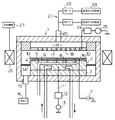
図1は、本実施形態に係るエッチング装置の全体の概略構成を模式的に示すもので、同図において、符号1は、材質が例えばアルミニウム等からなり、内部を気密に閉塞可能に構成された円筒状の真空チャンバを示している。
【0028】
上記真空チャンバ1内には、下部電極を兼ねた基板載置台2が設けられており、この基板載置台2は、セラミックなどの絶縁板3を介して真空チャンバ1の底部から支持されている。
【0029】
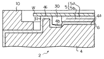
この基板載置台2は、図2に示すように、導電性部材、例えばアルミニウム等から円盤状に構成された基台部4の上面に、静電チャック部5を接着剤6で接着して構成されており、この静電チャック部5は、例えばAl2 O3 等のセラミックスからなる絶縁性部材5a内に、例えばタングステン等からなるチャック用電極5bを配置して構成されている。
【0030】
図1に示すように、上記チャック用電極5bには、直流電源7が接続されている。また、基台部4内には、温度調節媒体として、例えば冷却用の絶縁性流体を循環させるための流路8と、静電チャック部5の載置面と半導体ウエハWの裏面との間にヘリウム等の温調ガスを供給するためのガス流路9が形成されており、これらの機構によって、基板載置台2上に配置された半導体ウエハWを所定温度に温度調節できるように構成されている。さらに、静電チャック部5の周囲を囲むように、導電性材料または絶縁性材料で環状に形成されたフォーカスリング10が設けられている。
【0031】
また、基台部4のほぼ中央には、高周波電力を供給するための給電線11が接続されている。この給電線11にはマッチングボックス12及び高周波電源13が接続され、高周波電源12からは、所定周波数、例えば、数百KHz〜百数十MHzの範囲の高周波電力が、基台部4に供給されるようになっている。
【0032】
さらに、フォーカスリング10の外側には、環状に構成され、多数の排気孔が形成された排気リング14が設けられており、この排気リング14を介して、排気ポート15に接続された排気系16により、真空チャンバ1内の処理空間の真空排気が行われるよう構成されている。
【0033】
一方、基板載置台2の上方の真空チャンバ1の天壁部分には、シャワーヘッドを構成する上部電極17が、基板載置台2と平行に対向する如く設けられており、この上部電極17と基板載置台(下部電極)2が、一対の電極として機能するようになっている。
【0034】
上記上部電極17には、その下面に多数のガス吐出孔18が設けられている。また、上部電極17の上側には、ガス拡散用空隙19が形成されており、このガス拡散用空隙19の天井部には、ガス供給配管20が接続されている。そして、このガス供給配管20の他端には、エッチング用の処理ガス(エッチングガス)を供給する処理ガス供給系21が接続されている。処理ガス供給系21は、マスフローコントローラ(MFC)22及び処理ガス供給源23等から構成されている。
【0035】
また、上部電極17には、マッチングボックス24及び高周波電源25が接続され、高周波電源25からは、所定周波数、例えば、数百KHz〜百数十MHzの範囲の高周波電力が供給されるようになっている。
【0036】
一方、真空チャンバ1の外側周囲には、真空チャンバ1と同心状に、環状の磁場形成機構(リング磁石)26が配置されており、基板載置台2と上部電極17との間の処理空間に磁場を形成するようになっている。この磁場形成機構26は、回転機構27によって、その全体が、真空チャンバ1の回りを所定の回転速度で回転可能とされている。
【0037】
そして、本実施形態では、図2に示すように、基板載置台2の基台部4と静電チャック部5との接着剤6による接着部の周囲を囲むように、空隙部30が設けられており、この空隙部30に、図1に示したガス流路9からヘリウム等の温調ガスが供給され、接着剤6がプラズマ処理中に腐食性の高いフッ素ラジカル等を含む処理ガスと接触しないように構成されている。
【0038】
すなわち、基台部4上面の中央部には、静電チャック部5より僅かに小径とされた接着面4aが形成され、この接着面4aの周囲には、接着面より低い環状の溝部4bが形成されている。また、この溝部4bの周囲に、上方に突出する環状の凸部4cが形成されており、この凸部4cの上面の高さは、静電チャック部5の上面と同一高さになるよう構成され、静電チャック部5に半導体ウエハWが吸着保持されると、この半導体ウエハWの周縁部の下面が、凸部4cの上面に当接されるようになっている。
【0039】
そして、静電チャック部5に半導体ウエハWが吸着保持された状態では、溝部4bの上側が半導体ウエハWによって閉塞され、完全に気密ではないものの、外部との間のガスの流通をある程度遮断された状態の空隙部30が形成されるようになっている。この空隙部30には、上述したとおり、図1に示したガス流路9からヘリウム等の温調ガスが供給されるが、この温調ガスは、通常の場合数100乃至数千Pa(数Torr乃至数十Torr)程度のガス圧とされる。
【0040】
一方、プラズマ処理の際の処理ガスの圧力は、かかる圧力の1/10乃至1/100以下程度であるため、空隙部30から真空チャンバ1の処理空間内へのガスの流れは生じるが、逆に真空チャンバ1の処理空間内から空隙部30へのガスの流れが生じる可能性は極めて低くなる。
【0041】
したがって、接着剤6がプラズマ処理中に腐食性の高いフッ素ラジカル等を含む処理ガスと接触する可能性は極めて低くなり、かかるガスによる接着剤6の浸食を、略完全に防止することができる。このため、基台部4と静電チャック部5の間の接着状態を長期に亘って良好な状態に保つことができ、半導体ウエハWの温度上昇の発生等を防止することができるとともに、基板載置台2に関するメンテナンスの周期を長期化することができるので、従来に比べて装置稼働率の向上と、ランニングコストの低減を図ることができる。
【0042】
なお、図2に示すように、基台部4の外周面及び凸部4cの上面等には、Al2 O3 等のセラミックス溶射膜等からなる絶縁膜31が形成されている。
【0043】
このうち、凸部4cの上面、つまり、半導体ウエハWとの接触面には、予め必要とされる膜厚さよりも僅かに厚い膜厚、例えば膜厚が300〜400μmの絶縁膜31が形成され、基台部4に静電チャック部5を接着した後、凸部4cの上面の絶縁膜31と静電チャック部5の上面とを同時に表面研磨することにより、静電チャック部5の上面の高さと、凸部4cの上面の高さとを精度良く合せるようにして製造されている。
【0044】
また、上記したとおり、基台部4上面の接着面4aの周囲には、接着面4aより高さの低い溝部4bが形成され、ここに段差が設けられている。この段差は、基台部4に静電チャック部5を接着する際に、余分な接着剤6が、基台部4と静電チャック部5との間から段差によって溝部4b内に流れ易くするためのものである。
【0045】
さらに、基台部4上面の接着面4aは、静電チャック部5より僅かに小径とされており、この結果、静電チャック部5の外周部は、この接着面4aの周囲から僅かにオーバーハングするように、外周に突出した構造となっている。かかる構造も、基台部4に静電チャック部5を接着する際に、余分な接着剤6が、基台部4と静電チャック部5との間から外周側に流れ易くするためのものである。
【0046】
本実施形態では、上記構成を採用することによって、所望量の接着剤6を基台部4と静電チャック部5との間に介在させた状態(接着剤5の厚さが例えば70〜100μm程度)で、静電チャック部5と基台部4とを所定位置に精度良く接着できるようになっている。
【0047】
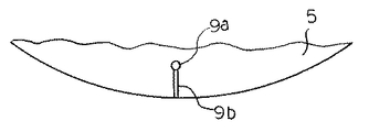
なお、ガス流路9から空隙部30へのヘリウム等の温調ガスの供給は、例えば、図3に示すように、静電チャック部5(絶縁性部材5a)を貫通して設けられ、半導体ウエハWの裏面に温調ガスを供給する透孔9aのうち、最外周部に設けられた透孔9aから静電チャック部5の外周縁部に至る細孔9b(例えば、幅1mm、深さ30〜50μm程度の細孔)を設けることによって行うことができる。このような構成を採用すれば、静電チャック部5に僅かな加工を施すだけで、空隙部30にヘリウム等の温調ガスを供給することができるが、その他の構成を採用することも勿論可能である。
【0048】
次に、上記のように構成されたエッチング装置によるエッチング手順について説明する。
【0049】
まず、真空チャンバ1に設けられた図示しない開閉機構を開放し、図示しない搬送機構により半導体ウエハWを真空チャンバ1内に搬入し、基板載置台2上に載置する。そして、直流電源7から静電チャック5のチャック用電極5bに所定の電圧を印加し、半導体ウエハWをクーロン力等により吸着する。
【0050】
この後、搬送機構を真空チャンバ1外へ退避させた後、開閉機構を閉じ、排気系16の真空ポンプにより排気ポート15を通じて真空チャンバ1内を排気する。真空チャンバ1内が所定の真空度になった後、真空チャンバ1内には、処理ガス供給系21から、所定のエッチングガスが、所定流量で導入され、真空チャンバ1内が所定の圧力、例えば1.33〜133Pa(10〜1000mTorr)に保持される。
【0051】
そして、この状態で高周波電源13、25から、基板載置台2の基台部4及び上部電極17に、所定周波数(例えば数百KHz〜百数十MHz)の高周波電力を供給する。
【0052】
この場合に、下部電極である基板載置台2と上部電極17との間の処理空間には高周波電界が形成されるとともに、磁場形成機構26による磁場が形成され、この状態でプラズマによる半導体ウエハWのエッチング処理が行われる。
【0053】
このエッチング処理の際に、基板載置台2の流路8には、冷却用の絶縁性流体が循環され、また、ガス流路9を通じて、基板載置台2の静電チャック部5と、半導体ウエハWの裏面との間には、ヘリウム等の温調ガスが供給されることによって、半導体ウエハWは、所定温度に保たれる。これとともに、上記ヘリウム等の温調ガスは、前述した細孔9bを介して空隙部30に供給されるので、接着剤6がプラズマ処理中に腐食性の高いフッ素ラジカル等を含む処理ガスと接触することが防止される。
【0054】
そして、所定のエッチング処理が実行されると、高周波電源13、25からの高周波電力の供給を停止することによって、エッチング処理を停止し、上述した手順とは逆の手順で、半導体ウエハWを真空チャンバ1外に搬出する。
【0055】
なお、上述した実施形態では、本発明を、上部電極と下部電極の双方に高周波電力を供給するタイプのエッチング装置に適用した例について説明したが、本発明はかかる場合に限定されるものではなく、例えば、下部電極にのみ高周波電力を供給するタイプのエッチング装置や、成膜を行うプラズマ処理装置等、あらゆるプラズマ処理装置に適用することができる。
【0056】
【発明の効果】
以上説明したとおり、本発明のプラズマ処理装置用電極及びプラズマ処理装置及びプラズマ処理装置用の基台部によれば、基台部と静電チャック部との間の接着状態を長期に亘って良好な状態に保つことができ、被処理基板の温度上昇の発生等を防止することができるとともに、従来に比べて装置稼働率の向上と、ランニングコストの低減を図ることができる。
【図面の簡単な説明】
【図1】本発明の一実施形態のプラズマ処理装置の全体の概略構成を示す図。
【図2】図1のプラズマ処理装置の基板載置台の要部概略構成を拡大して示す図。
【図3】図1のプラズマ処理装置の基板載置台の要部概略構成を拡大して示す図。
【符号の説明】
W……半導体ウエハ、1……真空チャンバ、2……基板載置台、4……基台部、4a……接着面、4b……溝部、4c……凸部、5……静電チャック部、6……接着剤、30……空隙部、31……絶縁膜。[0001]
BACKGROUND OF THE INVENTION
The present invention relates to a substrate mounting table for a plasma processing apparatus, a plasma processing apparatus, and a base for a plasma processing apparatus , and more particularly, generates plasma and uses this plasma to etch a substrate to be processed such as a semiconductor wafer. The present invention relates to a substrate mounting table for a plasma processing apparatus that performs a film forming process, a plasma processing apparatus, and a base for a plasma processing apparatus .
[0002]
[Prior art]
2. Description of the Related Art Conventionally, plasma processing apparatuses that generate plasma and cause the plasma to act on an object to be processed to perform a predetermined process have been widely used.
[0003]
For example, in the field of semiconductor device manufacturing, when forming a fine circuit structure of a semiconductor device, plasma is applied to a substrate to be processed such as a semiconductor wafer to perform an etching process or a film forming process.
[0004]
In such a plasma processing apparatus, since the substrate to be processed is disposed in the plasma processing chamber in the vacuum chamber in a reduced pressure atmosphere, it is difficult to suck and hold the substrate to be processed by the vacuum chuck, For this reason, many use an electrostatic chuck as a mechanism for attracting and holding the substrate to be processed. The electrostatic chuck is configured by disposing an electrostatic chuck electrode made of tungsten or the like between insulating members such as ceramics, and a DC voltage is applied to the electrostatic chuck electrode so that a coulomb is applied. The substrate to be processed is sucked and held by force or the like.
[0005]
In a so-called parallel plate type plasma processing apparatus, since the substrate mounting table on which the substrate to be processed is mounted also serves as the lower electrode, the basic component (base) of the substrate mounting table is made of aluminum or the like. It is necessary to configure with a conductive metal or the like.
[0006]
For this reason, the substrate mounting table is configured by bonding an insulating member (made of ceramics or the like) of an electrostatic chuck portion formed separately to a base portion made of aluminum or the like with an adhesive. Is known.
[0007]
[Problems to be solved by the invention]
However, in the conventional substrate mounting table described above, members having different coefficients of thermal expansion, that is, a base part made of aluminum or the like and an electrostatic chuck part made of ceramics or the like have to be bonded. It is necessary to use a highly adhesive such as a silicon-based adhesive.
[0008]
On the other hand, when plasma processing is performed in the plasma processing chamber, a highly corrosive process gas, for example, a process gas containing fluorine radicals or the like is used.
[0009]
For this reason, as the plasma processing is performed, the adhesive gradually changes in quality due to the process gas, resulting in a state of being eroded, resulting in a problem that the bonding state between the base portion and the electrostatic chuck portion becomes poor. there were.
[0010]
As described above, when the adhesion state between the base part and the electrostatic chuck part becomes poor, the base part and the electrostatic chuck part are in a state of being thermally insulated by vacuum, and the temperature control effect is obtained. There is a problem that the temperature is significantly lowered and the temperature of the substrate to be processed is increased. Further, in order to prevent such a problem, it is necessary to perform maintenance at an early stage to replace the substrate mounting table, which causes a problem that the operating rate of the apparatus is reduced and the running cost is increased.
[0011]
The present invention has been made in response to such a conventional situation, and can maintain a good adhesion state between the base portion and the electrostatic chuck portion over a long period of time. The substrate mounting table for the plasma processing apparatus, the plasma processing apparatus, and the base for the plasma processing apparatus can prevent the occurrence of the rise and the like, and can improve the apparatus operating rate and reduce the running cost as compared with the prior art. It is intended to provide a pedestal .
[0012]
[Means for Solving the Problems]
That is, the substrate mounting table for a plasma processing apparatus according to claim 1 is configured by disposing an electrode for electrostatic chuck between insulating members, and an electrostatic chuck portion for attracting and holding the substrate to be processed; A substrate mounting table for a plasma processing apparatus disposed in a plasma processing chamber, comprising: a base portion made of a member and provided with a cooling mechanism; and an adhesive portion for bonding the electrostatic chuck portion and the base portion with an adhesive. And formed in an annular shape so as to surround the electrostatic chuck portion at a predetermined interval from the electrostatic chuck portion, and the upper surface of the electrostatic chuck portion is a lower surface of the peripheral edge portion of the substrate to be processed. The upper surface of the substrate to be processed is formed between the contact portion to be contacted and the electrostatic chuck portion and the contact portion, and the substrate to be processed is placed on the electrostatic chuck portion. Sky configured to be covered by A part, characterized by comprising a gap portion provided so as to surround the periphery of the adhesive portion, and a gas introduction mechanism for introducing a predetermined gas into said gap portion.
[0015]
Further, the substrate mounting table for a plasma processing apparatus according to
[0016]
Further, the substrate mounting table for a plasma processing apparatus according to claim 3 is the substrate mounting table for the plasma processing apparatus according to
[0017]
The substrate mounting table for a plasma processing apparatus according to
[0018]
The substrate mounting table for a plasma processing apparatus according to
[0019]
The substrate mounting table for a plasma processing apparatus according to
[0020]
The plasma processing apparatus for a substrate mounting table of claim 7, in claim 1 to 6 for a plasma processing apparatus substrate mounting table of any one of claims, wherein the gas is warm for temperature control of the substrate to be treated It is a conditioning gas.
[0021]
The substrate mounting table for a plasma processing apparatus according to
[0022]
The substrate mounting table for a plasma processing apparatus according to claim 9 is the substrate mounting table for a plasma processing apparatus according to
[0023]
A plasma processing apparatus substrate mounting table according to
[0024]
The plasma processing apparatus for a substrate mounting table of claim 11, in claim 1-10 for a plasma processing apparatus substrate mounting table of any one of claims, the gas pressure in the gap portion than the pressure of the plasma processing chamber It is characterized by being expensive.
[0025]
A plasma processing apparatus according to a twelfth aspect includes the substrate mounting table for a plasma processing apparatus according to any one of the first to eleventh aspects.
The adhesive, base portion for plasma processing apparatus according to
[0026]
DETAILED DESCRIPTION OF THE INVENTION
Embodiments in which the present invention is applied to an electrode for an etching apparatus and an etching apparatus will be described below with reference to the drawings.
[0027]
FIG. 1 schematically shows an overall schematic configuration of an etching apparatus according to the present embodiment. In FIG. 1, reference numeral 1 is made of, for example, aluminum and is configured to be airtightly closed. A cylindrical vacuum chamber is shown.
[0028]
A substrate mounting table 2 also serving as a lower electrode is provided in the vacuum chamber 1, and the substrate mounting table 2 is supported from the bottom of the vacuum chamber 1 through an insulating plate 3 such as ceramic.
[0029]
As shown in FIG. 2, the substrate mounting table 2 is configured by adhering an
[0030]
As shown in FIG. 1, a DC power source 7 is connected to the chuck electrode 5b. Further, in the
[0031]
A power supply line 11 for supplying high-frequency power is connected to substantially the center of the
[0032]
Further, an
[0033]
On the other hand, an
[0034]
The
[0035]
In addition, a
[0036]
On the other hand, an annular magnetic field forming mechanism (ring magnet) 26 is disposed around the outside of the vacuum chamber 1 concentrically with the vacuum chamber 1, and is disposed in a processing space between the substrate mounting table 2 and the
[0037]
In this embodiment, as shown in FIG. 2, a
[0038]
That is, an adhesive surface 4a having a slightly smaller diameter than the
[0039]
In the state where the semiconductor wafer W is attracted and held on the
[0040]
On the other hand, since the pressure of the processing gas during the plasma processing is about 1/10 to 1/100 or less of the pressure, a gas flow from the
[0041]
Therefore, the possibility that the adhesive 6 comes into contact with a processing gas containing highly corrosive fluorine radicals or the like during plasma processing is extremely low, and erosion of the adhesive 6 by such gas can be almost completely prevented. For this reason, the adhesion state between the
[0042]
As shown in FIG. 2, an insulating film 31 made of a ceramic sprayed film such as Al 2 O 3 is formed on the outer peripheral surface of the
[0043]
Among these, on the upper surface of the convex portion 4c, that is, the contact surface with the semiconductor wafer W, an insulating film 31 having a thickness slightly larger than a required thickness, for example, a thickness of 300 to 400 μm is formed. Then, after the
[0044]
Further, as described above, a groove 4b having a height lower than that of the adhesive surface 4a is formed around the adhesive surface 4a on the upper surface of the
[0045]
Furthermore, the adhesive surface 4a on the upper surface of the
[0046]
In the present embodiment, by adopting the above configuration, a desired amount of the adhesive 6 is interposed between the
[0047]
The temperature control gas such as helium is supplied from the gas flow path 9 to the
[0048]
Next, an etching procedure using the etching apparatus configured as described above will be described.
[0049]
First, an opening / closing mechanism (not shown) provided in the vacuum chamber 1 is opened, and a semiconductor wafer W is loaded into the vacuum chamber 1 by a transfer mechanism (not shown) and placed on the
[0050]
Thereafter, after the transfer mechanism is retracted out of the vacuum chamber 1, the opening / closing mechanism is closed, and the inside of the vacuum chamber 1 is exhausted through the
[0051]
In this state, high-frequency power of a predetermined frequency (for example, several hundred KHz to several tens of MHz) is supplied from the high-
[0052]
In this case, a high-frequency electric field is formed in the processing space between the substrate mounting table 2 that is the lower electrode and the
[0053]
During this etching process, a cooling insulating fluid is circulated in the
[0054]
Then, when the predetermined etching process is executed, the etching process is stopped by stopping the supply of the high-frequency power from the high-
[0055]
In the above-described embodiment, the example in which the present invention is applied to an etching apparatus that supplies high-frequency power to both the upper electrode and the lower electrode has been described. However, the present invention is not limited to this case. For example, the present invention can be applied to any plasma processing apparatus such as an etching apparatus that supplies high-frequency power only to the lower electrode and a plasma processing apparatus that performs film formation.
[0056]
【The invention's effect】
As described above, according to the electrode for a plasma processing apparatus, the plasma processing apparatus, and the base part for the plasma processing apparatus of the present invention, the adhesion state between the base part and the electrostatic chuck part is good over a long period of time. Thus, the temperature rise of the substrate to be processed can be prevented, and the operating rate of the apparatus can be improved and the running cost can be reduced as compared with the prior art.
[Brief description of the drawings]
FIG. 1 is a diagram showing an overall schematic configuration of a plasma processing apparatus according to an embodiment of the present invention.
2 is an enlarged view showing a schematic configuration of a main part of a substrate mounting table of the plasma processing apparatus of FIG. 1;
3 is an enlarged view showing a schematic configuration of a main part of a substrate mounting table of the plasma processing apparatus of FIG. 1;
[Explanation of symbols]
W ... Semiconductor wafer, 1 ... Vacuum chamber, 2 ... Substrate mounting table, 4 ... Base part, 4a ... Adhesive surface, 4b ... Groove part, 4c ... Convex part, 5 ...
Claims (13)
導電性部材からなり冷却機構を具備した基台部と、
前記静電チャック部と前記基台部とを接着剤により接着する接着部と
を有する、プラズマ処理室内に配置されるプラズマ処理装置用基板載置台であって、
前記基台部に設けられ、前記静電チャック部の周囲を当該静電チャック部から所定間隔設けて囲むように環状に形成され、その上面が前記被処理基板の周縁部下面と当接する当接部と、
前記静電チャック部と前記当接部との間に形成され、かつ前記被処理基板が前記静電チャック部に載置された状態で、その上面が当該被処理基板によって覆われるように構成される空隙部であって、前記接着部の周囲を囲むように設けられた空隙部と、
前記空隙部に所定のガスを導入するガス導入機構と
を具備したことを特徴とするプラズマ処理装置用基板載置台。An electrostatic chuck portion configured to dispose an electrostatic chuck electrode between insulating members and hold the substrate to be processed by suction;
A base made of a conductive member and equipped with a cooling mechanism ;
An adhesive portion for bonding the electrostatic chuck portion and the base portion with an adhesive;
A substrate mounting table for a plasma processing apparatus disposed in a plasma processing chamber,
An abutment that is provided in the base portion and is formed in an annular shape so as to surround the electrostatic chuck portion with a predetermined interval from the electrostatic chuck portion, and an upper surface thereof abuts against a lower surface of a peripheral edge portion of the substrate to be processed. And
It is formed between the electrostatic chuck portion and the contact portion, and is configured such that the upper surface thereof is covered with the substrate to be processed in a state where the substrate to be processed is placed on the electrostatic chuck portion. A void portion provided so as to surround the periphery of the bonding portion ,
A substrate mounting table for a plasma processing apparatus, comprising: a gas introduction mechanism for introducing a predetermined gas into the gap portion.
前記当接部の少なくとも上面がセラミックスの溶射膜から形成されていることを特徴とするプラズマ処理装置用基板載置台。The substrate mounting table for a plasma processing apparatus according to claim 1 ,
A substrate mounting table for a plasma processing apparatus, wherein at least an upper surface of the contact portion is formed of a ceramic sprayed film.
前記基台部の前記静電チャック部との接着面が当該静電チャック部より小径とされ、前記接着面の周囲に当該接着面より高さの低い環状の溝部が形成され、前記静電チャック部の周縁部がオーハーハングして、前記接着面の周囲に突出するよう構成されていることを特徴とするプラズマ処理装置用基板載置台。The substrate mounting table for a plasma processing apparatus according to claim 1 or 2 ,
An adhesive surface of the base portion with the electrostatic chuck portion is made smaller in diameter than the electrostatic chuck portion, and an annular groove having a height lower than the adhesive surface is formed around the adhesive surface, and the electrostatic chuck A substrate mounting table for a plasma processing apparatus, wherein the peripheral edge of the part is overhanged and protrudes around the bonding surface.
前記基台部が導電性の金属から構成されていることを特徴とするプラズマ処理装置用基板載置台。The substrate mounting table for a plasma processing apparatus according to any one of claims 1 to 3 ,
The substrate mounting table for a plasma processing apparatus, wherein the base portion is made of a conductive metal.
前記金属がアルミニウムであることを特徴とするプラズマ処理装置用基板載置台。The substrate mounting table for a plasma processing apparatus according to claim 4 ,
A substrate mounting table for a plasma processing apparatus, wherein the metal is aluminum.
前記接着剤が、シリコン系の接着剤であることを特徴とするプラズマ処理装置用基板載置台。In the substrate mounting base for plasma processing apparatuses of any one of Claims 1-5 ,
The substrate mounting table for a plasma processing apparatus, wherein the adhesive is a silicon-based adhesive.
前記ガスが、前記被処理基板を温調するための温調用ガスであることを特徴とするプラズマ処理装置用基板載置台。In the substrate mounting base for plasma processing apparatuses of any one of Claims 1-6 ,
The substrate mounting table for a plasma processing apparatus, wherein the gas is a temperature adjusting gas for adjusting the temperature of the substrate to be processed.
前記温調用ガスが、前記静電チャック部の前記絶縁性部材に設けられた溝から前記空隙部に導入されることを特徴とするプラズマ処理装置用基板載置台。The substrate mounting table for a plasma processing apparatus according to claim 7 ,
The substrate mounting table for a plasma processing apparatus, wherein the temperature adjusting gas is introduced into the gap portion from a groove provided in the insulating member of the electrostatic chuck portion.
前記温調用ガスが、不活性ガスであることを特徴とするプラズマ処理装置用基板載置台。The substrate mounting table for a plasma processing apparatus according to claim 7 or 8 ,
The substrate mounting table for a plasma processing apparatus, wherein the temperature control gas is an inert gas.
前記不活性ガスが、ヘリウムガスであることを特徴とするプラズマ処理装置用基板載置台。The substrate mounting table for a plasma processing apparatus according to claim 9 ,
The substrate mounting table for a plasma processing apparatus, wherein the inert gas is helium gas.
前記空隙部内のガス圧が、前記プラズマ処理室内の圧力より高いことを特徴とするプラズマ処理装置用基板載置台。The substrate mounting table for a plasma processing apparatus according to any one of claims 1 to 10 ,
A substrate mounting table for a plasma processing apparatus, wherein a gas pressure in the gap is higher than a pressure in the plasma processing chamber.
前記静電チャック部の周囲を当該静電チャック部から所定間隔設けて囲むように環状に形成され、その上面が前記被処理基板の周縁部下面と当接する当接部と、
前記静電チャック部と前記当接部との間に形成され、かつ前記被処理基板が前記静電チャック部に載置された状態で、その上面が当該被処理基板によって覆われるように構成され、前記接着部の周囲を囲むように設けられた空隙部と
を具備し、前記空隙に所定のガスを導入するように構成された
ことを特徴とするプラズマ処理装置用の基台部。A base part for a plasma processing apparatus comprising a conductive member, having a cooling mechanism, and having an electrostatic chuck part for adsorbing and holding a substrate to be processed adhered by an adhesive part made of an adhesive,
An abutting portion that is formed in an annular shape so as to surround the electrostatic chuck portion with a predetermined interval from the electrostatic chuck portion, and an upper surface thereof abuts against a lower surface of a peripheral edge of the substrate to be processed;
It is formed between the electrostatic chuck portion and the contact portion, and is configured such that the upper surface thereof is covered with the substrate to be processed in a state where the substrate to be processed is placed on the electrostatic chuck portion. A gap provided to surround the periphery of the bonding portion;
And a base for a plasma processing apparatus , wherein a predetermined gas is introduced into the gap .
Priority Applications (1)
| Application Number | Priority Date | Filing Date | Title |
|---|---|---|---|
| JP2002202000A JP4033730B2 (en) | 2002-07-10 | 2002-07-10 | Substrate mounting table for plasma processing apparatus, plasma processing apparatus, and base for plasma processing apparatus |
Applications Claiming Priority (1)
| Application Number | Priority Date | Filing Date | Title |
|---|---|---|---|
| JP2002202000A JP4033730B2 (en) | 2002-07-10 | 2002-07-10 | Substrate mounting table for plasma processing apparatus, plasma processing apparatus, and base for plasma processing apparatus |
Publications (3)
| Publication Number | Publication Date |
|---|---|
| JP2004047653A JP2004047653A (en) | 2004-02-12 |
| JP2004047653A5 JP2004047653A5 (en) | 2005-10-27 |
| JP4033730B2 true JP4033730B2 (en) | 2008-01-16 |
Family
ID=31708310
Family Applications (1)
| Application Number | Title | Priority Date | Filing Date |
|---|---|---|---|
| JP2002202000A Expired - Fee Related JP4033730B2 (en) | 2002-07-10 | 2002-07-10 | Substrate mounting table for plasma processing apparatus, plasma processing apparatus, and base for plasma processing apparatus |
Country Status (1)
| Country | Link |
|---|---|
| JP (1) | JP4033730B2 (en) |
Families Citing this family (6)
| Publication number | Priority date | Publication date | Assignee | Title |
|---|---|---|---|---|
| US8491752B2 (en) | 2006-12-15 | 2013-07-23 | Tokyo Electron Limited | Substrate mounting table and method for manufacturing same, substrate processing apparatus, and fluid supply mechanism |
| JP2009188332A (en) | 2008-02-08 | 2009-08-20 | Tokyo Electron Ltd | Substrate-mounting stand for plasma processing apparatus, plasma processing apparatus and method of forming insulating film |
| JP5390846B2 (en) * | 2008-12-09 | 2014-01-15 | 東京エレクトロン株式会社 | Plasma etching apparatus and plasma cleaning method |
| JP6080571B2 (en) * | 2013-01-31 | 2017-02-15 | 東京エレクトロン株式会社 | Mounting table and plasma processing apparatus |
| JP2018107264A (en) * | 2016-12-26 | 2018-07-05 | 東京エレクトロン株式会社 | Consumption determining method and plasma processing device |
| JP7340938B2 (en) * | 2019-02-25 | 2023-09-08 | 東京エレクトロン株式会社 | Mounting table and substrate processing equipment |
-
2002
- 2002-07-10 JP JP2002202000A patent/JP4033730B2/en not_active Expired - Fee Related
Also Published As
| Publication number | Publication date |
|---|---|
| JP2004047653A (en) | 2004-02-12 |
Similar Documents
| Publication | Publication Date | Title |
|---|---|---|
| JP4935143B2 (en) | Mounting table and vacuum processing apparatus | |
| JP4547182B2 (en) | Plasma processing equipment | |
| JP5102500B2 (en) | Substrate processing equipment | |
| JP5492578B2 (en) | Plasma processing equipment | |
| CN105355585B (en) | Substrate mounting table of substrate processing apparatus | |
| JP2005033221A (en) | Substrate mounting stand and processor | |
| JPWO2003009363A1 (en) | Plasma processing apparatus and plasma processing method | |
| US20120006488A1 (en) | Ring-shaped component for use in a plasma processing, plasma processing apparatus and outer ring-shaped member | |
| JP6552346B2 (en) | Substrate processing equipment | |
| US7815492B2 (en) | Surface treatment method | |
| WO2002007212A1 (en) | Holding device for treated body | |
| JPWO2004084298A1 (en) | Substrate holding mechanism using electrostatic chuck and manufacturing method thereof | |
| JP2008251742A (en) | Substrate treating apparatus, and substrate mounting base on which focus ring is mounted | |
| JP7454976B2 (en) | Substrate support stand, plasma processing system, and edge ring replacement method | |
| KR101746567B1 (en) | Substrate attachment and detachment method, and substrate handling apparatus | |
| JP2018186179A (en) | Substrate processing apparatus and substrate removal method | |
| JP2008103403A (en) | Substrate mount table and plasma treatment apparatus | |
| KR101898079B1 (en) | Plasma processing apparatus | |
| JP4783094B2 (en) | Annular parts for plasma processing, plasma processing apparatus, and outer annular member | |
| WO2004021427A1 (en) | Plasma processing method and plasma processing device | |
| JP2007110023A (en) | Substrate holding apparatus | |
| JP4033730B2 (en) | Substrate mounting table for plasma processing apparatus, plasma processing apparatus, and base for plasma processing apparatus | |
| KR20160013792A (en) | Plasma processing apparatus | |
| JPH09289201A (en) | Plasma treating apparatus | |
| JP4972327B2 (en) | Plasma processing equipment |
Legal Events
| Date | Code | Title | Description |
|---|---|---|---|
| A521 | Written amendment |
Free format text: JAPANESE INTERMEDIATE CODE: A523 Effective date: 20050705 |
|
| A621 | Written request for application examination |
Free format text: JAPANESE INTERMEDIATE CODE: A621 Effective date: 20050705 |
|
| A977 | Report on retrieval |
Free format text: JAPANESE INTERMEDIATE CODE: A971007 Effective date: 20070419 |
|
| A131 | Notification of reasons for refusal |
Free format text: JAPANESE INTERMEDIATE CODE: A131 Effective date: 20070424 |
|
| A521 | Written amendment |
Free format text: JAPANESE INTERMEDIATE CODE: A523 Effective date: 20070622 |
|
| TRDD | Decision of grant or rejection written | ||
| A01 | Written decision to grant a patent or to grant a registration (utility model) |
Free format text: JAPANESE INTERMEDIATE CODE: A01 Effective date: 20071023 |
|
| A61 | First payment of annual fees (during grant procedure) |
Free format text: JAPANESE INTERMEDIATE CODE: A61 Effective date: 20071023 |
|
| FPAY | Renewal fee payment (event date is renewal date of database) |
Free format text: PAYMENT UNTIL: 20101102 Year of fee payment: 3 |
|
| R150 | Certificate of patent or registration of utility model |
Free format text: JAPANESE INTERMEDIATE CODE: R150 |
|
| FPAY | Renewal fee payment (event date is renewal date of database) |
Free format text: PAYMENT UNTIL: 20131102 Year of fee payment: 6 |
|
| LAPS | Cancellation because of no payment of annual fees |