JP4031998B2 - Wavelength multiplexing processor - Google Patents
Wavelength multiplexing processor Download PDFInfo
- Publication number
- JP4031998B2 JP4031998B2 JP2003042474A JP2003042474A JP4031998B2 JP 4031998 B2 JP4031998 B2 JP 4031998B2 JP 2003042474 A JP2003042474 A JP 2003042474A JP 2003042474 A JP2003042474 A JP 2003042474A JP 4031998 B2 JP4031998 B2 JP 4031998B2
- Authority
- JP
- Japan
- Prior art keywords
- wavelength
- light
- waveguide
- output
- incident
- Prior art date
- Legal status (The legal status is an assumption and is not a legal conclusion. Google has not performed a legal analysis and makes no representation as to the accuracy of the status listed.)
- Expired - Fee Related
Links
Images


Classifications
-
- G—PHYSICS
- G02—OPTICS
- G02B—OPTICAL ELEMENTS, SYSTEMS OR APPARATUS
- G02B6/00—Light guides; Structural details of arrangements comprising light guides and other optical elements, e.g. couplings
- G02B6/10—Light guides; Structural details of arrangements comprising light guides and other optical elements, e.g. couplings of the optical waveguide type
- G02B6/12—Light guides; Structural details of arrangements comprising light guides and other optical elements, e.g. couplings of the optical waveguide type of the integrated circuit kind
- G02B6/12007—Light guides; Structural details of arrangements comprising light guides and other optical elements, e.g. couplings of the optical waveguide type of the integrated circuit kind forming wavelength selective elements, e.g. multiplexer, demultiplexer
- G02B6/12009—Light guides; Structural details of arrangements comprising light guides and other optical elements, e.g. couplings of the optical waveguide type of the integrated circuit kind forming wavelength selective elements, e.g. multiplexer, demultiplexer comprising arrayed waveguide grating [AWG] devices, i.e. with a phased array of waveguides
- G02B6/12019—Light guides; Structural details of arrangements comprising light guides and other optical elements, e.g. couplings of the optical waveguide type of the integrated circuit kind forming wavelength selective elements, e.g. multiplexer, demultiplexer comprising arrayed waveguide grating [AWG] devices, i.e. with a phased array of waveguides characterised by the optical interconnection to or from the AWG devices, e.g. integration or coupling with lasers or photodiodes
- G02B6/12021—Comprising cascaded AWG devices; AWG multipass configuration; Plural AWG devices integrated on a single chip
-
- G—PHYSICS
- G02—OPTICS
- G02B—OPTICAL ELEMENTS, SYSTEMS OR APPARATUS
- G02B6/00—Light guides; Structural details of arrangements comprising light guides and other optical elements, e.g. couplings
- G02B6/24—Coupling light guides
- G02B6/26—Optical coupling means
- G02B6/35—Optical coupling means having switching means
- G02B6/351—Optical coupling means having switching means involving stationary waveguides with moving interposed optical elements
- G02B6/3512—Optical coupling means having switching means involving stationary waveguides with moving interposed optical elements the optical element being reflective, e.g. mirror
-
- G—PHYSICS
- G02—OPTICS
- G02B—OPTICAL ELEMENTS, SYSTEMS OR APPARATUS
- G02B6/00—Light guides; Structural details of arrangements comprising light guides and other optical elements, e.g. couplings
- G02B6/24—Coupling light guides
- G02B6/26—Optical coupling means
- G02B6/35—Optical coupling means having switching means
- G02B6/354—Switching arrangements, i.e. number of input/output ports and interconnection types
- G02B6/3544—2D constellations, i.e. with switching elements and switched beams located in a plane
- G02B6/3546—NxM switch, i.e. a regular array of switches elements of matrix type constellation
-
- G—PHYSICS
- G02—OPTICS
- G02B—OPTICAL ELEMENTS, SYSTEMS OR APPARATUS
- G02B6/00—Light guides; Structural details of arrangements comprising light guides and other optical elements, e.g. couplings
- G02B6/24—Coupling light guides
- G02B6/26—Optical coupling means
- G02B6/35—Optical coupling means having switching means
- G02B6/354—Switching arrangements, i.e. number of input/output ports and interconnection types
- G02B6/356—Switching arrangements, i.e. number of input/output ports and interconnection types in an optical cross-connect device, e.g. routing and switching aspects of interconnecting different paths propagating different wavelengths to (re)configure the various input and output links
Landscapes
- Physics & Mathematics (AREA)
- Engineering & Computer Science (AREA)
- Microelectronics & Electronic Packaging (AREA)
- General Physics & Mathematics (AREA)
- Optics & Photonics (AREA)
- Optical Integrated Circuits (AREA)
- Optical Communication System (AREA)
- Optical Couplings Of Light Guides (AREA)
- Mechanical Light Control Or Optical Switches (AREA)
- Use Of Switch Circuits For Exchanges And Methods Of Control Of Multiplex Exchanges (AREA)
Description
【0001】
【発明の属する技術分野】
本発明は、波長分割多重(WDM)システムにおいて使用される波長多重処理装置に関し、特に、導波路光学系と空間光学系を組み合わせた波長多重処理装置に関するものである。
【0002】
【従来の技術】
インターネットにおける加入者数の増加とアプリケーションの発展を背景に、IP(Internet Protocol)ネットワークは世界的な急成長を続けている。そのインフラである伝送ネットワークに対する需要が爆発的に増大している。とくにIT(Information Technology)先進国の北米でこの傾向は著しく、通信事業者は、増大する需要に対応する伝送ネットワークとして、WDM(Wavelength Division Multiplexing:波長分割多重)伝送システムへの投資を活発化させ、これを用いた光ネットワークの構築を急いでいる。
【0003】
WDM伝送システムのネットワーク構成の一例を図7(a),図7(b)および図8(a),図8(b)に示す。図7(a)は、複数のリングネットワークが相互につながれており(図中には2つのリング801,802のみを示した)、リング801,802どうしの接続部となる伝送装置803には、波長多重処理装置として、例えば図7(b)に示すような、任意の波長の光信号を入れ替え(即ち、クロスコネクト)を行なうためのクロスコネクト装置900をそなえている。
【0004】
すなわち、クロスコネクト装置900は、任意の波長の光信号を入れ替えることができるものであって、図7(b)に示すように、リング801,802を伝搬する波長多重光信号について波長多重分離処理を行なう多重分離処理部901〜904および波長分離されたリング801,802からの各波長の光信号についてリング801またはリング802へ切り替えて出力しうる光スイッチ905をそなえている。
【0005】
たとえば、図中リング801を左回りで入力される波長多重光信号S1を多重分離処理部901にて波長分離するとともに、図中リング802を右回りで入力される波長多重光信号S2を多重分離処理部902にて波長分離して、光スイッチ905で各波長の光信号の出力先リングが切り替えられる。光スイッチ905は、この出力先リングについて波長ごとに任意に設定することができるようになっている。
【0006】
なお、光スイッチ905によりリング801に出力される光信号は多重分離処理部903で他の波長の光信号と波長多重されてから送出され、光スイッチ905によりリング802に出力される光信号は多重分離処理部904で他の波長の光信号と波長多重されてから送出される。
図8(a)は、WDM伝送システムのネットワークとしての他の構成例を示すものであるが、この図8(a)に示すものにおいては、リングネットワーク804に伝送装置805を通じて装置806がローカル接続されている。この装置806においては、伝送装置805にそなえられた波長多重処理装置としての光分岐挿入装置910を介して、リングネットワーク804を伝搬する任意の波長信号を取り出し、同時に同一波長で別の信号光をリングネットワーク804に乗せることができるようになっている。
【0007】
図8(b)は伝送装置805における光分岐挿入装置(OADM:Optical Add Drop Multiplexer)910を示す図であるが、この光分岐挿入装置910は、リング804を伝搬する波長多重光信号について波長多重分離処理を行なう多重分離処理部911,912および波長分離されたリング804からの各波長の光信号についてリング804または装置806へ切り替えて出力しうる光スイッチ913をそなえている。
【0008】
たとえば、図中リング804を左回りで入力される波長多重光信号S3を多重分離処理部911にて波長分離して、光スイッチ913で各波長の光信号の出力先がリングネットワーク804又は装置806に切り替えられる。光スイッチ913は、この出力先について波長ごとに任意に設定することができるようになっている。
【0009】
ところで、上述のクロスコネクト装置900又は分岐挿入装置910としては、公知技術として、図9に示すような、AWG〔Arrayed Waveguide Grating:アレイ導波路型波長合分波器,図10(a),図10(b)参照〕を2つ(AWR1,AWR2)用いて実現したものがある(特許文献1参照)。図9に示すものにおいては、波長多重された光信号をAWGおよび透過型平面回折格子を用いて波長分離された複数の光信号に分解し、微小機械傾斜ミラースイッチ610の二次元アレイで反射させて、光分岐挿入を行なっている。
【0010】
すなわち、入力(IN)ポートから入射された波長多重光のうちで、通過させる波長の光信号についてはレンズ608側に反射させて、光サーキュレータ601を通じて通過(PASS)ポートに出力する一方、ドロップさせる波長の光信号についてはレンズ611側に反射させて、光サーキュレータ602を通じてドロップ(DROP)ポートに出力するようになっている。又、アド(ADD)ポートからアドさせる光信号については、レンズ608側に反射させて、光サーキュレータ601を通じて通過(PASS)ポートに出力するようになっている。
【0011】
さらに、特許文献2には、マイクロティルトミラーとともに回折格子を用いることにより、光分岐挿入を行なう技術について開示されている。
なお、本願発明に関連する技術として、特許文献3にて開示された技術もあるが、この特許文献3にて開示された技術は、光分岐挿入処理やクロスコネクト処理を行なうものではない。
【0012】
【特許文献1】
特開2000−347065号公報
【特許文献2】
米国特許第5,960,133号明細書
【特許文献3】
特開平11−95051号公報
【0013】
【発明が解決しようとする課題】
しかしながら、特許文献1にて開示された技術においては、2つのAWGと2つの光サーキュレータが必要であるために装置製造のためのコストが高くなるほか、部品点数が多いため装置サイズが大きくなるという課題がある。
また、特許文献2にて開示された技術においては、クロスコネクト機能を実現することができず、又、波長多重数の増大に対応した配置を実現することが困難である。
【0014】
本発明はこのような課題に鑑み創案されたもので、波長合分波を行なうためのAWGを1つだけにして、低コスト、小型化、低損失な波長多重処理装置を提供することを目的とする。
【0015】
【課題を解決するための手段】
このため、本発明の波長多重処理装置は、光信号が入射される第1入力ポートおよび第2入力ポートと、該光信号が出射される第1出力ポートおよび第2出力ポートと、基板上に、該第1入力ポートおよび該第2入力ポートならびに該第1出力ポートおよび該第2出力ポートに接続された複数の入出射導波路と、該複数の入出射導波路に接続された第1スラブ導波路と、該第1スラブ導波路に接続された互いの長さの異なる複数のチャネル導波路とが形成され、波長多重された波長多重光が該第1入力ポートまたは該第2入力ポートを介して該光信号として該複数の入出射導波路に入射された場合に、該波長多重光を該第1スラブ導波路で拡散して、該複数のチャンネル導波路で長さに応じた位相差を生じさせて出射する導波路デバイスと、入射される光の光路に対応して、面方向の角度切替が可能な反射ミラーが配列されたミラーアレイを少なくとも一つ有してなるミラーアレイデバイスと、該導波路デバイスから出射された該波長多重光について光路の異なる波長成分ごとに集光して、該ミラーアレイデバイスにおける該波長成分ごとに対応する反射ミラーへ出射するとともに、該反射ミラーからの反射光を該波長成分ごとに該チャンネル導波路に入射させるレンズデバイスとをそなえ、特定の波長成分に対しては、該第1入力ポートから該導波路デバイスを介して入射される該特定の波長成分に対する反射光を、該該導波路デバイスを介して該第2出力ポートに出射させるとともに、該第2入力ポートから該導波路デバイスを介して入射される該特定の波長成分に対する反射光を、該導波路デバイスを介して該第1出力ポートに出射させ、該特定の波長成分とは異なる他の波長成分に対しては、該第1入力ポートから該導波路デバイスを介して入射される該他の波長成分に対する反射光を、該導波路デバイスを介して該第1出力ポートに出射させるとともに、該第2入力ポートから該導波路デバイスを介して入射される該他の波長成分に対する反射光を、該導波路デバイスを介して該第2出力ポートに出射させるように、上記の入射される光信号成分が反射する反射ミラーの面方向角度を設定するように構成されたことを特徴としている(請求項1)。
【0016】
また、該ミラーアレイを複数そなえて該ミラーアレイデバイスが構成され、特定の波長成分に対しては、該第1入力ポートから該導波路デバイスを介して入射される該特定の波長成分に対する反射光を、該該導波路デバイスを介して該第2出力ポートに出射させるとともに、該第2入力ポートから該導波路デバイスを介して入射される該特定の波長成分に対する反射光を、該導波路デバイスを介して該第1出力ポートに出射させ、該特定の波長成分とは異なる他の波長成分に対しては、該第1入力ポートから該導波路デバイスを介して入射される該他の波長成分に対する反射光を、該導波路デバイスを介して該第1出力ポートに出射させるとともに、該第2入力ポートから該導波路デバイスを介して入射される該他の波長成分に対する反射光を、該導波路デバイスを介して該第2出力ポートに出射させるように、該複数のミラーアレイのそれぞれの反射ミラーが協働して面方向角度を設定するように構成され、かつ、該レンズデバイスが、該複数のチャンネル導波路から出射される光信号成分の焦点位置上に配置された導波路側レンズにより構成されることとしてもよい(請求項2)。
【0017】
さらに、該ミラーアレイデバイスが一つのミラーアレイをそなえて構成され、該レンズデバイスが、該複数のチャンネル導波路から出射される光信号成分の焦点位置上に配置された導波路側レンズと、該ミラーアレイをなす反射ミラーに対応して配列された複数の反射ミラー側レンズからなるレンズアレイとにより構成されることとしてもよい(請求項3)。
【0018】
また、該複数の入出射導波路から入射される光信号成分についてクロスコネクト処理を行なうべく、上記の入射される光信号成分が反射する反射ミラーの面方向角度を設定するように構成されることとしてもよい(請求項4)。
さらに、該複数の入出射導波路のいずれかから入射される光信号成分について、上記光信号成分が入射される導波路以外の導波路を通じて光分岐挿入処理を行なうべく、上記の入射される光信号成分が反射する反射ミラーの面方向角度を設定するように構成されることとしてもよい(請求項5)。
【0019】
【発明の実施の形態】
以下、図面を参照することにより、本発明の実施の形態を説明する。
〔A〕AWG(アレイ導波路格子)の説明
以下、本発明の各実施形態における波長多重処理装置の構成についての理解を助けるために、一般的に知られているAWGの構成について説明する。
【0020】
図10(a)はAWGの構成を模式的に示す上視図で、図10(b)はAWGの波長分光特性に着目して模式的に示す上視図である。
この図10(a)に示す一般的なAWG700は、基板701上に、少なくとも1本〔図10(a)中においては4本〕の入力導波路702,入力側スラブ導波路703,複数本のチャンネル導波路704,出力側スラブ導波路705および複数本の出力導波路706が形成されたものであって、入力導波路702のいずれかに、光ファイバなどを通じて外部から波長多重光(例えばλ1〜λ3の波長多重光)が入力されると、波長分離された光はそれぞれ別個の出力導波路706から出力されるようになっている。
【0021】
ここで、入力側スラブ導波路703においては、入力導波路702から伝搬してきた光を回折により拡散させるもので、各チャンネル導波路704は、互いに異なる導波路長の導波路が当該導波路長に応じて順次配列されたものであって、入力側スラブ導波路703で拡散した光を伝搬する一方、それぞれ導波路において伝搬する光同士で位相差を生ぜしめるものである。
【0022】
さらに、出力側スラブ導波路705は、各チャンネル導波路704からの放射光を互いに干渉せしめ、出力導波路706との接続部付近を焦点位置として集光させるものである。この出力導波路706との接続部付近での焦点位置としては、一本の入力導波路702から波長多重光が入射された場合には、同一波長成分の光が互いに異なる焦点位置で集光される。
【0023】
換言すれば、チャンネル導波路704間の長さの差により生じた位相差により集光する位置は波長によって異なるので、入力導波路702から波長多重光を入力すると、結果的に、波長ごとに異なる出力導波路706から出力される(分光される)ことになる。これにより、各出力導波路706では、上述の出力側スラブ導波路705で集光された互いに異なる波長の光を伝搬させることができるようになっている。
【0024】
なお、図10(b)に示すように、波長多重光を入力するポート(波長多重光を入射させる入力導波路702)を一つだけずらすと、分光される光も1ポートずれる。即ち、各波長の光が出力される出力導波路706についても、1つだけずれた出力導波路706から出力される。これは、チャンネル導波路704群への入射角度が1ポート分ずれるので、角度ずれによる位相整合角度が出射側でも1ポート分の角度だけずれるためである。
【0025】
たとえば、図10(b)中上から3番目の入力導波路702から波長多重光(Pλ1〜λ5)を入射した場合には、図10(b)中上から1番目〜5番目の出力導波路706からそれぞれ波長分波光Pλ1〜Pλ5が出力されるが、図10(b)中上から2番目の入力導波路702から波長多重光(Qλ1〜λ5)を入射した場合には、図10(b)中上から2番目〜6番目の(ポート位置がずれた)出力導波路706からそれぞれ波長分波光Qλ1〜Qλ5が出力されるのである。
【0026】
AWG700は、上述のごとく多重化された波長多重光を波長分離することができるほか、反対側の出力導波路706から各波長の信号光を入れることによって入力導波路701に波長多重された光を出力することができるようになっている。
この場合において、波長分離光を入力するポートとしての出力導波路706を一つだけずらすと、波長多重されて出射される入力導波路702についても1ポートずれる。即ち、波長分離光が入射される出力ポート位置によって、波長多重光が出射される入力導波路702のポート位置も1つだけずれる。
【0027】
たとえば、図10(b)中上から1番目〜5番目の出力導波路706からそれぞれ波長分波光Pλ1〜Pλ5を入射した場合には、図10(b)中上から3番目の入力導波路702から波長多重光(Pλ1〜λ5)が出力されるが、図10(b)中上から2番目〜6番目の出力導波路706からそれぞれ波長分波光Qλ1〜Qλ5を入射した場合には、図10(b)中上から(ポート位置がずれた)2番目の入力導波路702から波長多重光(Qλ1〜λ5)が出力されるのである。
【0028】
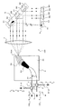
〔B〕第1実施形態の説明
図1は本発明の第1実施形態にかかる波長多重処理装置を示す模式図で、この図1に示す波長多重処理装置100は、2つの入力ポート(第1,第2入力ポート)としての光ファイバ7−1,8−1からの波長多重光についてクロスコネクト処理を施して、2つの出力ポート(第1,第2出力ポート)としての光ファイバ7−2,8−2から出力するものである。
【0029】
また、この図1に示す波長多重処理装置100は、光サーキュレータ1,2および光ファイバ7,7−1,7−2,8,8−1,8−2からなる入出力光インターフェイス部9をそなえるとともに、導波路デバイスとしてのAWG3,レンズ4およびミラーアレイ5,6をそなえて構成されている。
ここで、この図1に示すAWG3は、2本の入力導波路702を有するAWG700〔前述の図10(a),図10(b)参照〕について、各チャンネル導波路704が端面で垂直に分断されるように基板701を切断したものと等価である。
【0030】
すなわち、AWG3は、基板30上に、前述の図10(a),図10(b)で示したもの〔符号702〜704参照〕と基本的に同様の入出射導波路31,32,(第1)スラブ導波路33および複数の〔図1中においては5本の〕チャンネル導波路34が連続的に一体形成されている。つまり、基板30上に、光信号が入射または出射される入出射導波路31,32と、入出射導波路31,32に接続された(第1)スラブ導波路33と、スラブ導波路33に接続された互いに長さの異なる複数のチャンネル導波路34とが形成されている。
【0031】
また、チャンネル導波路34は、チャンネル導波路形成端面30Aにより垂直に分断され、チャンネル導波路34の端部が1直線上に並んでいるので、レンズ4との光学的な結合を低損失化させている。
なお、図1において、AWG3の入出射導波路31には、第1入力ポートとしての光ファイバ7−1からの光信号(波長多重光)が入射されるとともに、第1出力ポートとしての光ファイバ7−2に向けてクロスコネクト処理後の光信号(波長多重光)が出射されるようになっており、光ファイバ7および光サーキュレータ(第1サーキュレータ)1を介して第1の入出力ポートとしての光ファイバ7−1,7−2に接続されている。
【0032】
また、入出射導波路32には、第2入力ポートとしての光ファイバ8−1からの光信号(波長多重光)が入射されるとともに、第2出力ポートとしての光ファイバ8−2に向けてクロスコネクト処理後の光信号(波長多重光)が出射されるようになっており、光ファイバ8および光サーキュレータ(第2サーキュレータ)2を介して第2の入出力ポートとしての光ファイバ8−1,8−2に接続されている。
【0033】
また、第1実施形態におけるAWG3においては、入出射導波路31,32からの波長多重光について、スラブ導波路33で拡散して、チャンネル導波路34で導波路長に応じた位相差を生じさせているが、この位相差が生じた光は基板30におけるチャンネル導波路形成端面30Aからレンズ4に向けて出射されるようになっている。即ち、スラブ導波路33およびチャンネル導波路34が協働することにより、波長多重光を回折および干渉により波長によってそれぞれ異なる方向に分光されて、端面30Aから出射されるのである。
【0034】
さらに、AWG3において、後段のレンズ4からチャンネル導波路形成端面30Aに入射された光については、入出射導波路31,32から出力ポートとしての光ファイバ7−2,8−2に向けて、クロスコネクト処理後の波長多重光として出射されるようになっている。
また、レンズ(導波路側レンズ)4は、複数のチャンネル導波路34から出射される光信号成分の焦点位置上に配置されたもので、チャンネル導波路形成端面30Aから出射された光について、波長毎に異なる位置の焦点位置で集光させるとともに、各波長の光を互いに異なる光路を有する平行光として後段のミラーアレイ5に出射するものである。
【0035】
また、レンズ4は、後段のミラーアレイ5,6からの反射光についてチャンネル導波路形成端面30Aに対して出射するようになっている。従って、AWG3のチャンネル導波路形成端面30Aとレンズ4とは、入射および出射方向において光学的に接続され、チャンネル導波路形成端面30Aとレンズ4との間は、前述の図10(a),図10(b)に示す出力側スラブ導波路705と同様の機能を有している。
【0036】
さらに、ミラーアレイ(第1ミラーアレイ)5は、レンズ4と光学的に接続されるとともに、第2ミラーアレイ6との光軸を、少なくとも複数のチャンネル導波路37の光軸に重ならない向きとなるように配置され、第2ミラーアレイ6は、第1ミラーアレイ5からの入射光を当該第1ミラーアレイ5に反射するように配置されている。
【0037】
また、ミラーアレイデバイスを構成するミラーアレイ5,6はそれぞれ、入射される光の光路に対応して、面方向切替が可能な反射ミラー(以下、単にミラーと記載する場合がある)51〜56,61〜66が配列されたものであって、レンズ4からの平行光を反射して、レンズ4に再び戻すものである。
特に、これらのミラー51〜56,61〜66は、入出力される波長多重光の波長数および入出射導波路31,32の本数に応じて配列されて、光路の異なる平行光は互いに異なるミラー51〜56,61〜66で反射されるようになっている。本実施形態のミラーアレイ5,6においては、波長多重数(3波長)および入出射導波路31,32の本数(2本)に基づいて、それぞれ6枚のミラー51〜56,61〜66が配列されているのである。
【0038】
換言すれば、前述のレンズ4は、複数の入出射導波路31,32に波長多重された光信号が入射された場合に、複数のチャンネル導波路34から出射された光信号成分について光路の異なる光信号成分ごとに集光して、ミラーアレイデバイス5,6における対応するミラー51〜56,61〜66へ出射するとともに、これらのミラーからの反射光をチャンネル導波路34の端面30Aに入射させるレンズデバイスとして機能するようになっている。
【0039】
また、ミラー51〜56,61〜66は、入出射導波路31,32に入射される光信号成分が反射するが、このときのミラー51〜56,61〜66の面方向角度の切り替え設定により、光クロスコネクト処理のために、これらの入射光に対する反射光を入出射導波路31,32のいずれかから出射させるようにしている。
【0040】
すなわち、入出射導波路31,32のうちのいずれかから入射される光信号成分に対する反射光を出射させる導波路を、入出射導波路31,32のいずれかに設定すべく、ミラーアレイのそれぞれの反射ミラー51〜56,61〜66が協働して面方向角度を設定するようになっているのである。
ここで、ミラー51は、光ファイバ8−1からの波長λ1の分波光Pλ1をレンズ4から平行光として入射されて、面方向の角度切替により、ミラーアレイ6側のミラー61又は62に宛てて反射させるものであり、ミラー52は、光ファイバ7−1からの波長λ1の分波光Qλ1をレンズ4から平行光として入射されて、面方向の角度切替により、ミラーアレイ6側のミラー61又は62に宛てて反射させるものである。
【0041】
ミラー61,62は、ミラー51,52と協働して面方向の角度が切り替えられて、ミラー51,52を通じて入射された光を同一の光路で反射させたり、互いの光路が入れ替わった反射光をレンズ4に出射させたりするためのものである。
なお、図1中においては、分波光Pλ1についてはミラー51でミラー61に向けて反射させ、分波光Qλ1についてはミラー52でミラー61に宛てて反射させるように、ミラー51,52の面方向が切り替えられている。更に、ミラー61については、ミラー51,52からの分波光Pλ1および分波光Qλ1について、それぞれミラー52,51に反射されるように面方向の角度が切り替えられている。
【0042】
また、ミラー52で反射されたミラー61からの分波光Pλ1については、AWG3を通じて光ファイバ7−2に出射される光路でレンズ4に出射され、ミラー51で反射されたミラー62からの分波光Qλ1については、AWG3を通じて光ファイバ8−2に出射される光路でレンズ4に出射される。
さらに、ミラー53は、光ファイバ8−1からの波長λ2の分波光Pλ2をレンズ4から平行光として入射されて、面方向の角度切替により、ミラーアレイ6側のミラー63又は64に宛てて反射させるものであり、ミラー54は、光ファイバ7−1からの波長λ2の分波光Qλ2をレンズ4から平行光として入射されて、ミラーアレイ6側のミラー63又は64に宛てて反射させるものである。
【0043】
ミラー63,64は、ミラー53,54と協働して面方向の角度が切り替えられて、ミラー53,54を通じて入射された光を同一の光路で反射させたり、互いの光路が入れ替わった反射光をレンズ4に出射させたりするためのものである。
なお、図1中においては、分波光Pλ2についてはミラー53でミラー63に向けて反射させ、分波光Qλ2についてはミラー54でミラー64に宛てて反射させるように、ミラー53,54の面方向が切り替えられている。
【0044】
また、ミラー63,64はそれぞれ、ミラー53,54からの分波光Pλ2および分波光Qλ2について、それぞれもとの光路でレンズ4側に反射されるように面方向の角度が切り替えられている。即ち、ミラー63に反射された分波光Pλ2については、AWG3を通じて光ファイバ8−2に出射される光路でレンズ4に出射され、ミラー64に反射された分波光Qλ2については、AWG3を通じて光ファイバ7−2に出射される光路でレンズ4に出射される。
【0045】
さらに、ミラー55は、光ファイバ8−1からの波長λ3の分波光Pλ3をレンズ4から平行光として入射されて、面方向の角度切替により、ミラーアレイ6側のミラー65又は66に宛てて反射させるものであり、ミラー56は、光ファイバ7−1からの波長λ3の分波光Qλ3をレンズ4から平行光として入射されて、ミラーアレイ6側のミラー65又は66に宛てて反射させるものである。
【0046】
ミラー65,66は、ミラー55,56と協働して面方向の角度が切り替えられて、ミラー55,56を通じて入射された光を同一の光路で反射させたり、互いの光路が入れ替わった反射光をレンズ4に出射させたりするためのものである。
なお、図1中においては、分波光Pλ3についてはミラー55でミラー65に向けて反射させ、分波光Qλ3についてはミラー56でミラー66に宛てて反射させるように、ミラー55,56の面方向が切り替えられている。
【0047】
また、ミラー65,66はそれぞれ、ミラー55,56からの分波光Pλ3および分波光Qλ3について、それぞれもとの光路でレンズ4側に反射されるように面方向の角度が切り替えられている。即ち、ミラー65に反射された分波光Pλ3については、AWG3を通じて光ファイバ8−2に出射される光路でレンズ4に出射され、ミラー66に反射された分波光Qλ3については、AWG3を通じて光ファイバ7−2に出射される光路でレンズ4に出射される。
【0048】
これにより、AWG3においては、上述のごときレンズ4からの反射光をチャンネル導波路形成端面30Aで入射されて、それぞれの反射光の入射角に応じて2組の波長多重光に波長多重されて、それぞれ入出射導波路31,32を通じて出射させることができる。
なお、ミラーアレイ6は、レンズ4からミラーアレイ5への平行光に対してほぼ垂直となる角度に配置されている。これにより、ミラーアレイ6をなす反射ミラー61〜66の面方向角度を変化させることにより、AWG3と反射ミラー51〜56,61〜66との光結合効率を変化させることにより、波長ごとに任意の光透過強度を形成することができるようになっている。
【0049】
上述の構成による、本発明の第1実施形態にかかる波長多重処理装置100の動作について、以下に詳述する。
すなわち、光ファイバ7−1からの波長多重光<Qλ1,Qλ2,Qλ3>〔以下においては、波長多重光をなす光信号成分を<>内に示す〕は光サーキュレータ1および光ファイバ7を介してAWG3を構成する入出射導波路31に、光ファイバ8−1からの波長多重光<Pλ1,Pλ2,Pλ3>は光サーキュレータ2および光ファイバ8を介してAWG3の入出射導波路32に、それぞれ光クロスコネクト処理用に入射される。
【0050】
入出力光インターフェイス部9,AWG3,レンズ4およびミラーアレイ5,6からなる波長多重処理装置100においては、上述のごとく入出射導波路31,32に入射された2つの波長多重光についてクロスコネクト処理を行なって、例えば波長多重光<Pλ1,Qλ2,Qλ3>を入出射導波路31を通じて出射するとともに、波長多重光<Qλ1,Pλ2,Pλ3>を入出射導波路32を通じて出射する。
【0051】
すなわち、入出射導波路31に入射された波長多重光<Qλ1,Qλ2,Qλ3>はAWG3で分波され、各波長成分Qλ1,Qλ2,Qλ3がそれぞれミラー52,54,56で反射する〔図1における点線で示す光路を参照〕。このとき、波長成分Qλ2,Qλ3についてはミラー54,64,56,66が協働することで元の光路を通じて入出射導波路31から出射されるが、波長成分Qλ1についてはミラー52,61,51が協働することで入出射導波路8−2へ通じる光路で反射される〔図1におけるミラー52からミラー51およびミラー61に至る一点鎖線で示す光路を参照〕。
【0052】
また、入出射導波路32に入射された波長多重光<Pλ1,Pλ2,Pλ3>はAWG3で分波され、各波長成分Pλ1,Pλ2,Pλ3がそれぞれミラー51,53,55で反射する〔図1における実線で示す光路を参照〕。このとき、波長成分Pλ2,Pλ3についてはミラー53,63,55,65が協働することで元の光路を通じて入出射導波路32から出射されるが、波長成分Pλ1についてはミラー51,61,52が協働することで入出射導波路8−2へ通じる光路で反射される〔図1におけるミラー51からミラー61およびミラー52に至る一点鎖線で示す光路を参照〕。
【0053】
すなわち、波長多重光の信号成分をクロスコネクト処理により組み替える場合には、ミラーアレイ6において組み替え対象の波長〔図1の場合は波長λ1〕に割り当てられた2つのミラーのうちどちらか一つのミラー〔61〕のみに光が向くようにミラーアレイ5のミラー〔51,52〕の面方向角度を切り替える。更には、ミラーアレイ6のミラー〔61〕の向きは、ミラーアレイ5のうち1つの反射ミラー〔51,52〕からの反射光がもう一つの反射ミラー〔52,51〕に向かうように変化させる。
【0054】
したがって、ミラーアレイ5,6において対象となる波長成分〔Pλ1,Qλ1〕の光路が切り替えることにより、入射される波長多重光の信号成分を波長単位に組み替えて、クロスコネクト処理が施された波長多重光として入出射導波路31,32から出射することができるのである。λ1の光であるPλ1,Qλ1以外の波長成分Pλ2,Pλ3,Qλ2,Qλ3を組み替える場合についても同様である。
【0055】
なお、ミラーアレイ5,6では、それぞれの波長に分光された波長成分の信号光を反射させ、それぞれの波長に応じて選択的に方向を切り替えているが、反射されるミラー51〜56,61〜66の角度の調整により、反射光の光強度を適度に減衰させて、AWG3に戻すこともできる。このようにすれば、クロスコネクト装置としての機能とともに、波長ごとに光透過強度を可変する機能についても併せ持つ波長多重処理装置を構成することができる。
【0056】
このように、本発明の第1実施形態にかかる波長多重処理装置によれば、単一のAWG3を用いて光クロスコネクト機能を実現することができるので、装置を構成するための部品点数を減少させて、製造コストを大幅に削減させるとともに、装置規模の小型化を図ることができる利点がある。
また、第1ミラーアレイ5は、レンズ4と光学的に接続されるとともに、第2ミラーアレイ6との光軸を、少なくとも複数のチャンネル導波路34の光軸に重ならない向きとなるように配置され、第2ミラーアレイ6は、第1ミラーアレイ5からの入射光を当該第1ミラーアレイ5に反射するように配置されているので、ミラーアレイ6の面方向を導波路アレイ方向(AWG3の端部におけるチャンネル導波路34の形成方向)と垂直な方向に傾けて、導波路と反射ミラーとの光結合効率を変化させることにより、波長ごとに任意の光透過強度を形成することができ、波長等化器としての機能をも持たせることができる。
【0057】
〔B1〕第1実施形態の第1変形例の説明
図2は本発明の第1実施形態の第1変形例にかかる波長多重処理装置を示す模式図で、この図2に示す波長多重処理装置101は、前述の第1実施形態における波長多重処理装置100に比して、導波路デバイスとしてのAWG3−1の構成が異なっている。又、このAWG3−1以外の構成については、前述の波長多重処理装置100と同様であり、詳細な説明については省略する。尚、図2中、図1と同様の部分には同一の符号を付してある。
【0058】
ここで、AWG3−1は、図1に示すAWG3と異なり、基板30上に、光信号が入射または出射される入出射導波路31,32と、入出射導波路31,32に接続された(第1)スラブ導波路33と、スラブ導波路33に接続された互いに長さの異なる複数のチャンネル導波路34とともに、チャンネル導波路34に接続された長方形形状の出力側スラブ導波路(第2スラブ導波路)35が形成されている。
【0059】
そして、この出力側スラブ導波路35は、レンズ4と光学的に接続される端面30Bに沿って形成されており、これにより、AWG3―1は、出力側スラブ導波路35の形成端面30Bを通じてレンズ4と光学的に接続されている。
このような構成による、第1実施形態の第1変形例にかかる波長多重処理装置101においても、第1実施形態にかかる波長多重処理装置100と同様に、波長多重光についてのクロスコネクト処理を行なうことができる。
【0060】
したがって、第1実施形態の第1変形例にかかる波長多重処理装置101においても、前述の第1実施形態の場合と同様の利点を得ることができるほか、前述の第1実施形態においては、AWG3を製造する際に、チャンネル導波路34を端面30Aで垂直となる様な高精度の切断加工が必要となるが、本変形例によれば、各チャンネル導波路34を高精度な導波路プロセスのみで形成することができるので、各チャンネル導波路35の長さを高精度かつ容易に製造することができる利点もある。
【0061】
〔B2〕第1実施形態の第2変形例の説明
図3は本発明の第1実施形態の第2変形例にかかる波長多重処理装置を示す模式図で、この図3に示す波長多重処理装置102は、前述の図2に示す波長多重処理装置102に比して、導波路デバイスとしてのAWG3−2の構成が異なっている。又、このAWG3−2以外の構成については、前述の波長多重処理装置100,101と同様であり、詳細な説明については省略する。尚、図3中、図1,図2と同様の部分には同一の符号を付してある。
【0062】
ここで、AWG3−2は、図2に示すAWG3−1と異なり、出力側スラブ導波路36が、光伝搬方向の長さがスラブ導波路33よりも短くされている。そして、出力側スラブ導波路36が、レンズ4と光学的に接続される端面30Cに沿って形成されて、AWG3―2が出力側スラブ導波路35の形成端面30Cを通じてレンズ4と光学的に接続されている。
【0063】
このような構成による、第1実施形態の第2変形例にかかる波長多重処理装置102においても、第1実施形態にかかる波長多重処理装置100と同様に、波長多重光についてのクロスコネクト処理を行なうことができる。
したがって、第1実施形態の第2変形例にかかる波長多重処理装置102においても、前述の第1実施形態の第1変形例の場合と同様の利点を得ることができるほか、出力側スラブ導波路36を、図2の場合の出力側スラブ導波路35よりも光伝搬方向での長さを短くして形成しているので、レンズ4との焦点距離を短くすることができ、図2に示す波長多重処理装置の場合に比べて装置規模の縮小化を図ることができる利点がある。
【0064】
なお、上述の第1実施形態および第1実施形態の第1,第2変形例においては、光クロスコネクト機能および波長ごとの光透過強度可変機能を有しているが、光クロスコネクト機能に代えて光分岐挿入機能を持たせることも、もちろん可能である。
〔C〕第2実施形態の説明
図4は本発明の第2実施形態にかかる波長多重処理装置を示す模式図で、この図4に示す波長多重処理装置200は、前述の第1実施形態における波長多重処理装置100に比して、クロスコネクト機能及び波長ごとの光透過強度可変機能をそなえている点は共通するが、AWG230およびミラーアレイ250,260の構成が異なっており、更に、入出力ポートとしての光ファイバ7−1,7−2,8−1,8−2をAWG230と接続するための光サーキュレータ〔図1における符号1,2参照〕を不要としている。
【0065】
なお、第2実施形態にかかる波長多重処理装置200のミラー240は、前述の図1〜図3に示すレンズ4と同様の機能を有するものである。
また、AWG230は、基板231上に、4本の入出射導波路232〜235,スラブ導波路236および複数の(図4中では5本の)チャンネル導波路237が形成されたものであって、前述のAWG700〔前述の図10(a),図10(b)参照〕について、各チャンネル導波路704が端面で垂直に分断されるように基板701を切断したものと等価である。
【0066】
すなわち、基板231上に、光信号が入射または出射される入出射導波路232〜235と、入出射導波路232〜235に接続された(第1)スラブ導波路236と、スラブ導波路236に接続された互いに長さの異なるチャンネル導波路237と、が形成されている。又、チャンネル導波路237は、チャンネル導波路形成端面30Aにより垂直に分断され、複数のチャンネル導波路237の端部が1直線上に並んでいるので、レンズ4との光学的な結合を低損失化させている。
【0067】
また、AWG230は、前述の図1〜3に示すAWG3,3−1,3−2とは異なり、4本の入出射導波路232〜235をそなえているが、スラブ導波路236およびチャンネル導波路237については、AWG3,3−1,3−2におけるスラブ導波路33およびチャンネル導波路34と機能的には同様に構成されている。又、AWG230における4本の入出射導波路232〜236は、それぞれ光ファイバ7−1,7−2,8−1,8−2に接続されている。
【0068】
これにより、入出射導波路(第1入出射導波路)232は第1入力ポートとしての光ファイバ7−1から波長多重光が入射される入射導波路として構成され、入出射導波路(第2入出射導波路)235は第2入力ポートとしての光ファイバ8−1から波長多重光が入射される入射導波路として構成される。同様に、入出射導波路(第3入出射導波路)233は第1出力ポートとしての光ファイバ7−2に対してクロスコネクト処理後の第1の波長多重光を出射する出射導波路として構成され、入出射導波路(第4入出射導波路)234は第2出力ポートとしての光ファイバ8−2に対してクロスコネクト処理後の第2の波長多重光を出射する出射導波路として構成される。
【0069】
また、第2実施形態におけるAWG230においても、入射導波路232,235からの波長多重光について、スラブ導波路236で拡散して、チャンネル導波路237で導波路長に応じた位相差を生じさせているが、この位相差が生じた光は基板231におけるチャンネル導波路形成端面230Aからレンズ240に向けて出射されるようになっている。即ち、スラブ導波路236および各チャンネル導波路237が協働することにより、波長多重光を回折および干渉により波長によってそれぞれ異なる方向に分光して、端面230Aから出射されるようになっている。
【0070】
さらに、後段のミラーアレイ250,260からの反射光を、レンズ240を介しチャンネル導波路形成端面230Aを通じて入射されると、出射導波路233,234から出力ポートとしての光ファイバ7−2,8−2に向けて、クロスコネクト処理後の波長多重光として出射されるようになっている。
また、レンズ240(導波路側レンズ)は、複数のチャンネル導波路237から出射される光信号成分の焦点位置上に配置され、チャンネル導波路形成端面230Aから出射された光について、波長毎に異なる位置の焦点位置で集光させるとともに、各波長の光を互いに異なる光路を有する平行光として後段のミラーアレイ250に出射するものである。
【0071】
さらに、後段のミラーアレイ250,260からの反射光については、チャンネル導波路形成端面230Aに対して出射するようになっている。従って、AWG230のチャンネル導波路形成端面230Aとレンズ240とは、入射および出射方向において光学的に接続されており、チャンネル導波路形成端面230Aとレンズ240とは、前述の図10(a),図10(b)に示す出力側スラブ導波路705と同様の機能を有している。
【0072】
また、ミラーアレイ(第1ミラーアレイ)250は、レンズ240と光学的に接続されるとともに、第2ミラーアレイ260との光軸を、少なくとも複数のチャンネル導波路237の光軸に重ならない向きとなるように配置され、第2ミラーアレイ260は、第1ミラーアレイ250からの入射光を当該第1ミラーアレイ250に反射するように配置されている。
【0073】
さらには、ミラーアレイデバイスを構成するミラーアレイ250,260はそれぞれ、入射される光の光路に対応して面方向切替が可能な反射ミラー(以下、単にミラーと記載する場合がある)251−1〜251−4,252−1〜252−4,253−1〜253−4,261〜266が配列されたものであって、レンズ240からの平行光を反射して、レンズ240に再び戻すものである。
【0074】
特に、これらのミラー51〜56,61〜66は、入出力される波長多重光の波長数および入出射導波路232〜235の本数(入出力ポートのポート数)に応じて配列されて、光路の異なる平行光は互いに異なるミラーで反射されるようになっている。
本実施形態のミラーアレイ250においては、波長多重数(3波長)および入出射導波路232〜235の本数(4本)に基づいて、1波長あたり4枚のミラー251−1〜251−4,252−1〜252−4,253−1〜253−4が配列され、ミラーアレイ260においては、1波長あたり2枚のミラー261〜266が配列されているのである。
【0075】
換言すれば、前述のレンズ240は、複数の入射導波路232,235に波長多重された光信号が入射された場合に、複数のチャンネル導波路237から出射された光信号成分について光路の異なる光信号成分ごとに集光して、ミラーアレイ250,260における対応するミラー251−1,251−4,252−1,252−4,253−1,253−4,261〜266へ出射するとともに、これらの反射ミラーからの反射光をチャンネル導波路237の端面230Aに入射させるレンズデバイスとして機能するようになっている。
【0076】
また、入射導波路232,235に入射される光信号成分は反射するミラーアレ250,260における該当ミラーで反射するが、このときの該当ミラー251−1〜251−4,252−1〜252−4,253−1〜253−4,261〜266の面方向角度は、光クロスコネクト処理のために、上述の入射光に対する反射光を出射導波路233,234のいずれかから出射させるように切替設定されている。
【0077】
すなわち、入出射導波路232〜235のうちのいずれかから入射される光信号成分に対する反射光を入出射導波路232〜235のいずれかから出射させるように、ミラーアレイ250,260のそれぞれの反射ミラー251−1〜251−4,252−1〜252−4,253−1〜253−4,261〜266が協働して面方向角度を設定するように構成されている。
【0078】
ここで、ミラー251−1は、光ファイバ8−1からの波長λ1の分波光Pλ1をレンズ240から平行光として入射されて、面方向の角度切替により、ミラーアレイ260側のミラー261に宛てて反射させるものであり、ミラー251−4は、光ファイバ7−1からの波長λ1の分波光Qλ1をレンズ240から平行光として入射されて、面方向の角度切替により、ミラーアレイ260側のミラー262に宛てて反射させるものである。
【0079】
ミラー261,262は、ミラー251−2,251−2のいずれかと協働して面方向の角度が切り替えられて、ミラー251−1,251−4を通じて入射された光を、光ファイバ8−2を通じて出射させるための光路で反射させたり、光ファイバ7−2を通じて出射させるための光路で反射させたりするためのものである。
【0080】
なお、図1中においては、分波光Pλ1についてはミラー251−1でミラー261に向けて反射させ、分波光Qλ1についてはミラー251−4でミラー262に宛てて反射させるように、ミラー251−1,251−4の面方向が切り替えられている。更に、ミラー261,262についてはそれぞれ、ミラー251−1,251−4からの分波光Pλ1,Qλ1について、ミラー251−3,251−2に反射されるように面方向の角度が切り替えられている。
【0081】
また、ミラー251−3で反射されたミラー261からの分波光Pλ1については、AWG230を通じて光ファイバ7−2に出射される光路でレンズ240に出射され、ミラー251−2で反射されたミラー262からの分波光Qλ1については、AWG230を通じて光ファイバ8−2に出射される光路でレンズ240に出射される。
【0082】
さらに、ミラー252−1は、光ファイバ8−1からの波長λ2の分波光Pλ2をレンズ240から平行光として入射されて、面方向の角度切替により、ミラーアレイ260側のミラー263に宛てて反射させるものであり、ミラー252−4は、光ファイバ7−1からの波長λ2の分波光Qλ2をレンズ240から平行光として入射されて、ミラーアレイ260側のミラー264に宛てて反射させるものである。
【0083】
ミラー263,264は、ミラー252−2,252−3と協働して面方向の角度が切り替えられて、ミラー252−1,252−4を通じて入射された光を、光ファイバ8−2を通じて出射させるための光路で反射させたり、光ファイバ7−2を通じて出射させるための光路で反射させたりするためのものである。
なお、図1中においては、分波光Pλ2についてはミラー252−1でミラー263に向けて反射させ、分波光Qλ2についてはミラー252−4でミラー264に宛てて反射させるように、ミラー252−1,252−4の面方向が切り替えられている。
【0084】
また、ミラー263,264はそれぞれ、ミラー252−1,252−4からの分波光Pλ2および分波光Qλ2について、それぞれ光ファイバ8−2,7−2に通じた光路でレンズ240側に反射されるように面方向の角度が切り替えられている。即ち、ミラー263に反射された分波光Pλ2については、AWG230を通じて光ファイバ8−2に出射される光路でレンズ240に出射され、ミラー264に反射された分波光Qλ2については、AWG230を通じて光ファイバ7−2に出射される光路でレンズ240に出射される。
【0085】
さらに、ミラー253−1は、光ファイバ8−1からの波長λ3の分波光Pλ3をレンズ240から平行光として入射されて、面方向の角度切替により、ミラーアレイ260側のミラー265に宛てて反射させるものであり、ミラー253−4は、光ファイバ7−1からの波長λ3の分波光Qλ3をレンズ240から平行光として入射されて、ミラーアレイ260側のミラー266に宛てて反射させるものである。
【0086】
ミラー265,266は、ミラー253−2,253−3と協働して面方向の角度が切り替えられて、ミラー253−1,253−4を通じて入射された光を、光ファイバ8−2を通じて出射させるための光路で反射させたり、光ファイバ7−2を通じて出射させるための光路で反射させたりするためのものである。
なお、図1中においては、分波光Pλ3についてはミラー253−1でミラー265に向けて反射させ、分波光Qλ3についてはミラー253−4でミラー266に宛てて反射させるように、ミラー253−1,253−4の面方向が切り替えられている。
【0087】
また、ミラー265,266はそれぞれ、ミラー253−1,253−4からの分波光Pλ3および分波光Qλ3について、それぞれ光ファイバ8−2,7−2に通じた光路でレンズ240側に反射されるように面方向の角度が切り替えられている。即ち、ミラー265に反射された分波光Pλ3については、AWG230を通じて光ファイバ8−2に出射される光路でレンズ240に出射され、ミラー266に反射された分波光Qλ3については、AWG230を通じて光ファイバ7−2に出射される光路でレンズ240に出射される。
【0088】
これにより、AWG230においては、上述のごときレンズ240からの反射光をチャンネル導波路形成端面230Aで入射されて、それぞれの反射光の入射角に応じて2組の波長多重光に波長多重されて、それぞれ出射導波路233,234を通じて出射させることができる。
なお、ミラーアレイ260は、レンズ240からミラーアレイ250への平行光に対してほぼ垂直となる角度に配置されている。これにより、ミラーアレイ260をなす反射ミラー261〜266の面方向角度を変化させることにより、AWG230と反射ミラー251−1〜251−4,252−1〜252−4,253−1〜253−4,261〜266との光結合効率を変化させることにより、波長ごとに任意の光透過強度を形成することができるようになっている。
【0089】
上述の構成により、本発明の第2実施形態にかかる波長多重処理装置200においても、前述の第1実施形態における波長多重処理装置100と基本的に同様に、クロスコネクト処理を行なうことができる。
たとえば、光ファイバ7−1からの波長多重光<Qλ1,Qλ2,Qλ3>はAWG230を構成する入射導波路235に、光ファイバ8−1からの波長多重光<Pλ1,Pλ2,Pλ3>はAWG230の入射導波路232に、それぞれ光クロスコネクト処理用に入射される。
【0090】
AWG230,レンズ240およびミラーアレイ250,260からなる波長多重処理装置200においては、上述のごとく入射導波路232,235に入射された2つの波長多重光について、ミラーアレイ250,260をなす反射ミラー251−1〜251−4,252−1〜252−4,253−1〜253−4,261〜266の面方向角度を切り替えることでクロスコネクト処理を行なう。
【0091】
これにより、例えば波長多重光<Pλ1,Qλ2,Qλ3>を出射導波路233を通じて出射するとともに、波長多重光<Qλ1,Pλ2,Pλ3>を出射導波路234を通じて出射する。
このように、本発明の第2実施形態にかかる波長多重処理装置によれば、単一のAWG230を用いて光クロスコネクト機能を実現することができるので、装置を構成するための部品点数を減少させて、製造コストを大幅に削減させるとともに、装置規模の小型化を図ることができる利点があるほか、第1実施形態における波長多重処理装置の場合に必要であった光サーキュレータを不要とすることが可能であるため、部品点数を更に減少させ、製造コストの更なる低減化や装置規模の小型化を図るほか、光サーキュレータを光が通過する分の光損失までも低減させることもできる。
【0092】
また、前述の第1実施形態の場合と同様に、ミラーアレイ260の面方向を導波路アレイと垂直な方向に傾けて、導波路と反射ミラーとの光結合効率を変化させることにより、波長ごとに任意の光透過強度を形成することができ、波長等化器としての機能をも持たせることができる。
さらに、ミラーアレイ250は、レンズ240と光学的に接続されるとともに、第2ミラーアレイ260との光軸を、少なくとも複数のチャンネル導波路237の光軸に重ならない向きとなるように配置され、第2ミラーアレイ260は、第1ミラーアレイ250からの入射光を当該第1ミラーアレイ250に反射するように配置されているので、ミラーアレイ250,260における反射ミラーの面方向の切替において、各波長に分波された信号光をスイッチで反射させたときの光ビームを、ミレンズ240とミラーアレイ250との間の光路方向に垂直な方向に回避してから、光路切り替えを行なっているので、切替先となる出力ポート以外の他のポートへの不要信号の入射を防ぐこともできる。
【0093】
〔D〕第3実施形態の説明
図5は本発明の第3実施形態にかかる波長多重処理装置を示す模式図で、この図5に示す波長多重処理装置300は、光サーキュレータ1,2および光ファイバ7,7−1,7−2,8,8−1,8−2からなる入出力光インターフェイス部9をそなえるとともに、導波路デバイスとしてのAWG330,凸形状の第1レンズ341,マイクロレンズアレイ342およびミラーアレイ350をそなえて構成され、波長多重光について光分岐挿入処理を施すものである。
【0094】
すなわち、第3実施形態にかかる波長多重処理装置300においては、入力ポートとしての光ファイバ7−1からの波長多重光をなす複数の波長成分の光のうちのいずれかを、分岐ポートとしての光ファイバ8−2から選択的に出射させるとともに(ドロップ)、挿入ポートとしての光ファイバ8−1からの光を、上述の波長多重光をなす残りの波長成分の光と多重(波長多重)して(アド)、出力ポートとしての光ファイバ7−2から出射するようになっている。
【0095】
ここで、この図5に示すAWG330は、前述の第1実施形態におけるものと同様、基板335上に、光信号が入射または出射される入出射導波路331,332,(第1)スラブ導波路333および複数の〔図5中においては5本の〕チャンネル導波路334が連続的に一体形成されている。つまり、基板335上に、入出射導波路331,332と、入出射導波路331,332に接続された(第1)スラブ導波路333と、スラブ導波路333に接続された互いに長さの異なる複数のチャンネル導波路334とが形成されている。
【0096】
また、チャンネル導波路334は、チャンネル導波路形成端面330Aにより垂直に分断され、チャンネル導波路334の端部が1直線上に並んでいるので、後段のレンズ341との光学的な結合を低損失化させている。
また、AWG330の入出射導波路331には、光ファイバ7および光サーキュレータ1を介して入力ポートとしての光ファイバ7−1および出力ポートとしての光ファイバ7−2が接続されており、入力ポートとしての光ファイバ7−1からの光信号(波長多重光)が入射されるとともに、出力ポートとしての光ファイバ7−2に向けて分岐挿入処理後の光信号(波長多重光)が出射されるようになっている。
【0097】
さらに、入出射導波路332には、光ファイバ8および光サーキュレータ2を介して挿入ポートとしての光ファイバ8−1および分岐ポートとしての光ファイバ8−2が接続されており、光ファイバ8−1から挿入用の光が入射されるとともに、光ファイバ8−2に分岐光が出射されるようになっている。
また、上述の入出射導波路331,332から入射された光についても、スラブ導波路333で拡散して、チャンネル導波路334で、その導波路長に応じた位相差を生じさせているが、この位相差が生じた光は基板335におけるチャンネル導波路形成端面330Aから第1レンズ341に向けて出射されるようになっている。即ち、スラブ導波路333およびチャンネル導波路334が協働して波長多重光を回折および干渉させて、波長および入射された導波路331,332によってそれぞれ異なる方向に分光されるのである。
【0098】
さらに、AWG330において、後段の第1レンズ341からチャンネル導波路形成端面330Aに入射された光については、入出射導波路331,332から出力ポートとしての光ファイバ7−2または分岐ポートとしての光ファイバ8−2に向けて、分岐挿入処理後の波長多重光として出射されるようになっている。
【0099】
また、第1レンズ(導波路側レンズ)341は、前述の第1実施形態におけるレンズ4と同様に、複数のチャンネル導波路334から出射される光信号成分の焦点位置上に配置されている。そして、チャンネル導波路形成端面330Aから出射された光について、波長毎および入射された導波路331,332によって異なる焦点位置で集光させるとともに、各波長の光を互いに異なる光路を有する平行光として後段のマイクロレンズアレイ342側に出射するものであり、更に、後段のマイクロレンズアレイ342からの反射光についてチャンネル導波路形成端面330Aに対して出射するようになっている。
【0100】
したがって、AWG330のチャンネル導波路形成端面330Aとレンズ341とは、入射および出射方向において光学的に接続され、チャンネル導波路形成端面330Aとレンズ4との間は、前述の図10(a),図10(b)に示す出力側スラブ導波路705と同様の機能を有している。
また、マイクロレンズアレイ342は、凸形状に複数の反射ミラー側レンズとしての第2レンズ343〜345をそなえてなるものである。そして、これらの第2レンズ343〜345は、入射される波長多重光を構成する波長に対応して、AWG3で分光された各波長の光の光路上に配列されている。図5中におけるレンズ343〜345はそれぞれ、波長λ1〜λ3にそれぞれ対応して、波長λ1〜λ3の光の光路上に配置されたものである。
【0101】
すなわち、第2レンズ343〜345はそれぞれ、入力ポートとしての光ファイバ7−1から入射され分光された光Pλ1〜Pλ3と、挿入ポートとしての光ファイバ8−1から入射された光Qλ1〜Qλ3とを集光してミラーアレイ350に出射するとともに、ミラーアレイ350で反射された各波長の光を平行光として第1レンズ341に出射するようになっている。
【0102】
なお、第1レンズ341は分光された信号光すべてを1つの凸部で集光できる大きさであり、第2レンズ343〜345は分光された波長の光毎に異なるレンズ343〜345の凸部で集光できる大きさを有している。
ミラーアレイデバイスを構成するミラーアレイ350は、入射される光の光路に対応して面方向切替が可能な複数〔3つの〕の反射ミラー351〜353が配列されたものであって、これらの反射ミラー351〜353はそれぞれ、第2レンズ343〜345からの平行光を反射して、第2レンズ343〜345に再び戻すものである。
【0103】
換言すれば、上述の第1レンズ341および第2レンズ343〜345により、複数の入出射導波路331,332に波長多重された光信号が入射された場合に、複数のチャンネル導波路334から出射された光信号成分について光路の異なる光信号成分ごとに集光して、ミラーアレイデバイス350における対応するミラー351〜353へ出射するとともに、これらのミラー351〜353からの反射光をチャンネル導波路334の端面330Aに入射させるレンズデバイスとして機能するようになっている。
【0104】
また、入出射導波路331,332に入射される光信号成分が反射するミラー351〜353の面方向角度は、光分岐挿入処理のために、これらの入射光に対する反射光を入出射導波路331,332のいずれかから出射させるように設定されている。
たとえば、入力ポートとしての光ファイバ7−1から出力ポートとしての光ファイバ7−2に光を通す場合には、ミラーアレイ350における該当波長光を反射するミラー351〜353を、光を完全に反対向きに反射させるような面方向角度に設定する。このとき、反射光は元の光路を辿ってAWG330に戻されて、入出射導波路331を伝搬するため、光サーキュレータ1を経由して出力ポートとしての光ファイバ7−2へと導かれる。
【0105】
また、入力ポートとしての光ファイバ7−1から分岐ポートとしての光ファイバ8−2に光を通す場合には、ミラーアレイ350における該当波長光を反射するミラー351〜353の面角度を切り替えて、反射光の角度が、挿入ポートとしての光ファイバ8−1から入射された同一波長の光が端面330Aから出射される際の角度と同じになるようにしている。
【0106】
この場合において、AWG330に戻された信号光は入出射導波路332の方向に回折されるため、反射光は、光サーキュレータ2を経由して分岐ポートとしての光ファイバ8−2へと導かれる。このとき、挿入ポートとしての光ファイバ8−1に入射した光は入出射導波路331の方向に回折されるため、光サーキュレータ1を経由して出力ポートとしての光ファイバ7−2へと導かれる。従って、入力ポートから分岐ポートへの分岐スイッチングと、挿入ポートから出力ポートへの挿入スイッチングを同時に実現することができる。
【0107】
なお、図5中においては、λ1の光が入力ポートから分岐ポートへの分岐スイッチング〔Pλ1参照〕がなされるとともに、挿入ポートから出力ポートへの挿入スイッチング〔Qλ1参照〕がなされる状態〔ルーティング状態〕であり、波長λ2の光と波長λ3の光は、入力ポートから出力ポートへのスイッチングがなされる状態〔ルーティング状態〕である。
【0108】
上述の構成による、本発明の第3実施形態にかかる波長多重処理装置300の動作について、以下に詳述する。
すなわち、光ファイバ7−1からの波長多重光<Pλ1,Pλ2,Pλ3>〔以下においては、波長多重光をなす光信号成分を<>内に示す〕は光サーキュレータ1および光ファイバ7を介してAWG330を構成する入出射導波路331に、光ファイバ8−1からの挿入スイッチング用の光Pλ1は光サーキュレータ2および光ファイバ8を介してAWG330の入出射導波路332に、それぞれ光分岐処理用に入射される。
【0109】
入出力光インターフェイス部9,AWG330,第1レンズ341,マイクロレンズアレイ342およびミラーアレイ350からなる波長多重処理装置300においては、上述のごとく入出射導波路331,332に入射された2つの波長多重光について分岐挿入処理を行なって、例えば波長多重光<Qλ1,Pλ2,Pλ3>を入出射導波路331を通じて出射するとともに、分岐光Pλ1を入出射導波路332を通じて出射する。
【0110】
なお、ミラーアレイ350では、それぞれの波長に分光された波長成分の信号光を反射させ、それぞれの波長に応じて光分岐挿入処理のためにミラー角度を選択的に切り替えているが、反射されるミラー351〜353の角度の調整により、反射光の光強度を適度に減衰させて、AWG330に戻すこともできる。このようにすれば、光分岐挿入装置としての機能とともに、波長ごとに光透過強度を可変する機能についても併せ持つ波長多重処理装置を構成することができる。
【0111】
このように、本発明の第3実施形態にかかる波長多重処理装置によれば、単一のAWG330を用いて光分岐挿入機能を実現することができるので、装置を構成するための部品点数を減少させて、製造コストを大幅に削減させるとともに、装置規模の小型化を図ることができる利点がある。
また、ミラーアレイ350についても一つだけで構成することができるので、装置を構成するための部品点数を減少させて、製造コストを大幅に削減させるとともに、ミラーアレイ350をなす各反射ミラー351〜353の面方向の角度切替制御についても容易にすることができる利点もある。
【0112】
〔E〕第4実施形態の説明
図6は本発明の第4実施形態にかかる波長多重処理装置を示す模式図で、この図6に示す波長多重処理装置400は、前述の第3実施形態における波長多重処理装置300に比して、光分岐挿入機能及び波長ごとの光透過強度可変機能をそなえている点は共通するが、AWG430の構成が異なっており、更に、入出力ポートとしての光ファイバ7−1,7−2,8−1,8−2をAWG430と接続するための光サーキュレータ1,2や光ファイバ7,8を不要としている。
【0113】
また、AWG430は、前述の第2実施形態におけるAWG230と同様の構成を有しており、前述のAWG700〔前述の図10(a),図10(b)参照〕について、各チャンネル導波路704が端面で垂直に分断されるように基板701を切断したものと等価である。
すなわち、基板431上に、光信号が入射または出射される入出射導波路432〜435と、入出射導波路432〜435に接続された(第1)スラブ導波路436と、スラブ導波路436に接続された互いに長さの異なる複数のチャンネル導波路437とが形成されている。又、チャンネル導波路437は、チャンネル導波路形成端面30Aにより垂直に分断され、チャンネル導波路34の端部が1直線上に並んでいるので、レンズ4との光学的な結合を低損失化させている。
【0114】
ここで、AWG430は、4本の入出射導波路432〜435をそなえているが、スラブ導波路436およびチャンネル導波路437については、AWG3,3−1,3−2におけるスラブ導波路33およびチャンネル導波路34と機能的には同様に構成されている。又、AWG430における4本の入出射導波路432〜436は、それぞれ光ファイバ8−2,7−2,8−1,7−1に接続されている。
【0115】
これにより、入出射導波路432は分岐ポート(第2出力ポート)としての光ファイバ8−2に対して分岐された光を出射する出射導波路として構成され、入出射導波路433は(第1)出力ポートとしての光ファイバ7−2に対して光分岐挿入処理後の波長多重光を出射する出射導波路として構成される。同様に、入出射導波路434は挿入ポート(第2入力ポート)としての光ファイバ8−1から挿入処理用の光が入射される入射導波路として構成され、入出射導波路435は(第1)入力ポートとしての光ファイバ7−1から波長多重光が入射される入射導波路として構成される。
【0116】
したがって、入出射導波路432は第2出力ポートに接続された第4導波路として、入出射導波路433は第1出力ポートに接続された第3導波路として、入出射導波路434は第2入力ポートに接続された第2導波路として、入出射導波路435は第1入力ポートに接続された第1導波路として、それぞれ構成される。そして、4本の入出射導波路432〜435の配列は、第1入出射導波路,第2入出射導波路,第3入出射導波路および第4入出射導波路の順番で相対的に並んでいる。
【0117】
また、上述の入出射導波路434,435から入射された光についても、スラブ導波路436で拡散して、チャンネル導波路437で、その導波路長に応じた位相差を生じさせているが、この位相差が生じた光は基板431におけるチャンネル導波路形成端面430Aから第1レンズ441に向けて出射されるようになっている。即ち、スラブ導波路436およびチャンネル導波路437が協働して波長多重光を回折および干渉させて、波長および入射された導波路31,32によってそれぞれ異なる方向に分光されるのである。
【0118】
さらに、AWG430において、第1レンズ441からチャンネル導波路形成端面430Aに入射された光については、入出射導波路433,432から出力ポートとしての光ファイバ7−2または分岐ポートとしての光ファイバ8−2に向けて、分岐挿入処理後の波長多重光として出射されるようになっている。
また、第1レンズ441は、前述の第3実施形態におけるレンズ341と同様に、複数のチャンネル導波路437から出射される光信号成分の焦点位置上に配置されるものである。そして、チャンネル導波路形成端面430Aから出射された光について、波長毎および入射された導波路434,435によって異なる焦点位置で集光させるとともに、各波長の光を互いに異なる光路を有する平行光として後段のマイクロレンズアレイ442側に出射し、更に、後段のマイクロレンズアレイ442からの反射光についてはチャンネル導波路形成端面430Aに対して集光して出射するようになっている。
【0119】
したがって、AWG430のチャンネル導波路形成端面430Aとレンズ441とは、入射および出射方向において光学的に接続されるとともに、前述の図10(a),図10(b)に示す出力側スラブ導波路705と同様の機能を有している。
また、マイクロレンズアレイ442は、凸形状に複数の反射ミラー側レンズとしての第2レンズ443〜445をそなえてなるものである。そして、これらの第2レンズ443〜445は、入射される波長多重光を構成する波長に対応して、AWG3で分光された各波長の光の光路上に配列されている。図6中におけるレンズ443〜445はそれぞれ、波長λ1〜λ3にそれぞれ対応して、波長λ1〜λ3の光の光路上に配置されたものである。
【0120】
すなわち、第2レンズ443〜445はそれぞれ、入力ポートとしての光ファイバ7−1から入射され分光された光Pλ1〜Pλ3と、挿入ポートとしての光ファイバ8−1から入射された光Qλ1〜Qλ3とを集光してミラーアレイ450に出射するとともに、ミラーアレイ450で反射された各波長の光を平行光として第1レンズ441に出射するようになっている。
【0121】
なお、第1レンズ441は分光された信号光すべてを1つの凸部で集光できる大きさであり、第2レンズ343〜345は分光された波長の光毎に異なるレンズ443〜445の凸部で集光できる大きさを有している。
ミラーアレイデバイスを構成するミラーアレイ450は、入射される光の光路に対応して面方向切替が可能な複数〔3つの〕の反射ミラー451〜453が配列されたものであって、これらの反射ミラー451〜453はそれぞれ、第2レンズ443〜445からの平行光を反射して、第2レンズ443〜445に再び戻すものである。
【0122】
換言すれば、上述の第1レンズ441および第2レンズ443〜445により、入出射導波路435,434に光が入射された場合に、複数のチャンネル導波路437から出射された光信号成分について光路の異なる光信号成分ごとに集光して、ミラーアレイデバイス450における対応するミラー451〜453へ出射するとともに、これらのミラー451〜453からの反射光をチャンネル導波路437の端面430Aに入射させるレンズデバイスとして機能するようになっている。
【0123】
また、入出射導波路435,434に入射される光信号成分が反射するミラー451〜453の面方向角度は、光分岐挿入処理のために、これらの入射光に対する反射光を入出射導波路432,433のいずれかから出射させるように設定されている。
たとえば、入力ポートとしての光ファイバ7−1から出力ポートとしての光ファイバ7−2に光を通す場合には、ミラーアレイ450における該当波長光を反射するミラー451〜453の面角度を切り替えることにより、該当波長の反射光を入出射導波路433を伝搬するようにしている。これにより、該当波長光は出力ポートとしての光ファイバ7−2へと導かれる。
【0124】
また、入力ポートとしての光ファイバ7−1から分岐ポートとしての光ファイバ8−2に光を通す場合には、ミラーアレイ450における該当波長光を反射するミラー451〜453の面角度を切り替えて、該当波長の反射光を入出射導波路432を伝搬するようにしている。これにより、該当波長光は分岐ポートとしての光ファイバ8−2へと導かれる。
【0125】
このとき、挿入ポートとしての光ファイバ8−1に入射した光がAWG430,第1レンズ441およびマイクロレンズアレイ442を通じてミラーアレイ450に到達すると、その光は入出射導波路433を伝搬するような光路で反射されるので、出力ポートとしての光ファイバ7−2へと導かれる。従って、入力ポートから分岐ポートへの分岐スイッチングと、挿入ポートから出力ポートへの挿入スイッチングを同時に実現することができる。
【0126】
なお、図6中においては、λ1の光が入力ポートから分岐ポートへの分岐スイッチング〔Pλ1参照〕がなされるとともに、挿入ポートから出力ポートへの挿入スイッチング〔Qλ1参照〕がなされる状態〔ルーティング状態〕であり、波長λ2の光と波長λ3の光は、入力ポートから出力ポートへのスイッチングがなされる状態〔ルーティング状態〕である。
【0127】
上述の構成による、本発明の第4実施形態にかかる波長多重処理装置400の動作の一例について、以下に詳述する。
すなわち、光ファイバ7−1からの波長多重光<Pλ1,Pλ2,Pλ3>〔以下においては、波長多重光をなす光信号成分を<>内に示す〕はAWG430を構成する入出射導波路435に、光ファイバ8−1からの挿入スイッチング用の光Qλ1はAWG430の入出射導波路434に、それぞれ光分岐処理用に入射される。
【0128】
波長多重処理装置400においては、上述のごとく入出射導波路435,434に入射された光について、ミラー451〜453の面角度切替により分岐挿入処理を行なって、例えば波長多重光<Qλ1,Pλ2,Pλ3>を入出射導波路433を通じて出射するとともに、分岐光Pλ1を入出射導波路432を通じて出射する。
【0129】
なお、ミラーアレイ450では、それぞれの波長に分光された波長成分の信号光を反射させ、それぞれの波長に応じて光分岐挿入処理のためにミラー角度を選択的に切り替えているが、反射されるミラー451〜453の角度の調整により、反射光の光強度を適度に減衰させて、AWG430に戻すこともできる。このようにすれば、光分岐挿入装置としての機能とともに、波長ごとに光透過強度を可変する機能についても併せ持つ波長多重処理装置を構成することができる。
【0130】
このように、本発明の第4実施形態にかかる波長多重処理装置によれば、単一のAWG430を用いて光分岐挿入機能を実現することができるので、装置を構成するための部品点数を減少させて、製造コストを大幅に削減させるとともに、装置規模の小型化を図ることができる利点がある。
また、ミラーアレイ450についても一つだけで構成することができるので、装置を構成するための部品点数を減少させて、製造コストを大幅に削減させるとともに、ミラーアレイ350をなす各反射ミラー451〜453の面方向の角度切替制御についても容易にすることができる利点もある。
【0131】
さらに、AWG430により、第3実施形態における波長多重処理装置の場合に必要であった光サーキュレータを不要とすることが可能であるため、部品点数を更に減少させ、製造コストの更なる低減化や装置規模の小型化を図り、光サーキュレータを光が通過する分の光損失までも低減させることもできる。
〔F〕その他
上述の各実施形態における波長多重処理装置においては、入射される波長多重光の波長数は3波長である場合について詳述したが、本発明によればこれに限定されるものではなく、4波長以上の波長多重光についても入射して、光クロスコネクト処理や光挿入分岐処理を行なうことももちろん可能である。
【0132】
さらに、上述の各実施形態においては、入力ポートおよび出力ポートの数は、それぞれ2つずつとしているが、本発明によればこれに限定されず、2つ以上の入力ポートおよび出力ポートをそなえるように構成することも可能である。
さらに、上述の第2〜第4実施形態においては、AWG230,330,430として第2スラブ導波路が形成されていないものを用いているが、本発明によればこれに限定されず、第1実施形態の第1変形例あるいは第2変形例におけるAWG3−1,3−2のごとく、第2スラブ導波路35,36が形成されているものを用いることもでき、このようにすれば、第1実施形態の第1変形例あるいは第2変形例の場合と同様の利点を得ることができる。
【0133】
また、上述の各実施形態における態様によらず、本発明の趣旨を逸脱しない範囲で種々変形して実施することができる。
製造できる。
〔G〕付記
(付記1) 基板上に、光信号が入射または出射される複数の入出射導波路と、該複数の入出射導波路に接続された第1スラブ導波路と、該第1スラブ導波路に接続された互いに長さの異なる複数のチャンネル導波路とが形成された導波路デバイスと、
入射される光の光路に対応して、面方向の角度切替が可能な反射ミラーが配列されたミラーアレイを少なくとも一つ有してなるミラーアレイデバイスと、
該複数の入出射導波路に波長多重された光信号が入射された場合に、該複数のチャンネル導波路から出射された光信号成分について光路の異なる光信号成分ごとに集光して、該ミラーアレイデバイスにおける対応する反射ミラーへ出射するとともに、該反射ミラーからの反射光を該チャンネル導波路側の基板端面に入射させるレンズデバイスとをそなえ、
該複数の入出射導波路のうちのいずれかから入射される光信号成分に対する反射光を該複数の入出射導波路のいずれかから出射させるように、上記の入射される光信号成分が反射する反射ミラーの面方向角度を設定するように構成されたことを特徴とする、波長多重処理装置。
【0134】
(付記2) 該ミラーアレイを複数そなえて該ミラーアレイデバイスが構成され、該複数の入出射導波路のうちのいずれかから入射される光信号成分に対する反射光を該複数の入出射導波路のいずれかから出射させるように、該複数のミラーアレイのそれぞれの反射ミラーが協働して面方向角度を設定するように構成され、
かつ、該レンズデバイスが、該複数のチャンネル導波路から出射される光信号成分の焦点位置上に配置された導波路側レンズにより構成されたことを特徴とする、付記1記載の波長多重処理装置。
【0135】
(付記3) 該ミラーアレイデバイスが一つのミラーアレイをそなえて構成され、
該レンズデバイスが、該複数のチャンネル導波路から出射される光信号成分の焦点位置上に配置された導波路側レンズと、該ミラーアレイをなす反射ミラーに対応して配列された複数の反射ミラー側レンズからなるレンズアレイとにより構成されたことを特徴とする、付記1記載の波長多重処理装置。
【0136】
(付記4) 該複数の入出射導波路から入射される光信号成分についてクロスコネクト処理を行なうべく、上記の入射される光信号成分が反射する反射ミラーの面方向角度を設定するように構成されたことを特徴とする、付記1記載の波長多重処理装置。
(付記5) 該複数の入出射導波路のいずれかから入射される光信号成分について、上記光信号成分が入射される導波路以外の導波路を通じて光分岐挿入処理を行なうべく、上記の入射される光信号成分が反射する反射ミラーの面方向角度を設定するように構成されたことを特徴とする、付記1記載の波長多重処理装置。
【0137】
(付記6) 該導波路デバイスが、基板上に、光信号が入射または出射される複数の入出射導波路と、該複数の入出射導波路に接続された第1スラブ導波路と、該スラブ導波路に接続された互いに長さの異なる複数のチャンネル導波路とともに、該チャンネル導波路に接続された第2スラブ導波路が形成され、
かつ、該反射ミラーからの反射光を入射させる該チャンネル導波路側の基板端面には、該第2スラブ導波路が形成されていることを特徴とする、付記1記載の波長多重処理装置。
【0138】
(付記7) 該第2スラブ導波路の導波路長が、該第1スラブ導波路の導波路長よりも短くしてあることを特徴とする、付記6記載の波長多重処理装置。
(付記8) 該複数のチャンネル導波路端部が1直線上に並んでいることを特徴とする、付記1記載の波長多重処理装置。
(付記9) 該導波路デバイスをなす基板上に形成された複数の入出射導波路として、第1入出射導波路および第2入出射導波路がそなえられ、
該第1入出射導波路には第1光サーキュレータを介して第1入力ポートおよび第1出力ポートが接続され、該第2入出射導波路には第2光サーキュレータを介して第2入力ポートおよび第2出力ポートが接続されていることを特徴とする、付記1記載の波長多重処理装置。
【0139】
(付記10) 該導波路デバイスをなす基板上に形成された複数の入出射導波路として、上記光信号が入射される第1入出射導波路および第2入出射導波路ならびに光信号が出射される第3入出射導波路および第4入出射導波路をそなえるとともに、
該第1入出射導波路には第1入力ポートが接続され、該第2入出射導波路には第2入力ポートが接続され、該第3入出射導波路には第1出力ポートが接続され、該第4入出射導波路には第2出力ポートが接続されていることを特徴とする、付記1記載の波長多重処理装置。
【0140】
(付記11) 上記4本の導波路の配列が、該第1入出射導波路、該第2入出射導波路、該第3入出射導波路および該第4入出射導波路の順番で相対的に並んでいることを特徴とする、付記10記載の波長多重処理装置。
(付記12) 該第1入力ポートを光挿入分岐処理における入力ポート、該第2入力ポートを光挿入分岐処理における挿入ポート、該第1出力ポートを光挿入分岐処理における出力ポート、該第2出力ポートを光挿入分岐処理における分岐ポートとして構成されたことを特徴とする、付記9〜11のいずれか1項記載の波長多重処理装置。
【0141】
(付記13) 該複数のミラーアレイが、第1ミラーアレイおよび第2ミラーアレイにより構成され、該第1ミラーアレイが、該レンズデバイスと光学的に接続されるとともに、第2ミラーアレイとの光軸を、少なくとも該複数のチャンネル導波路の光軸に重ならない向きとなるように配置され、
該第2ミラーアレイは、該第1ミラーアレイからの入射光を当該第1ミラーアレイに反射するように配置されていることを特徴とする、付記1記載の波長多重処理装置。
【0142】
【発明の効果】
以上詳述したように、本発明の波長多重処理装置によれば、単一の導波路デバイスを用いて光クロスコネクト機能や光分岐挿入機能を実現することができるので、装置を構成するための部品点数を減少させて、製造コストを大幅に削減させるとともに、装置規模の小型化を図ることができる利点がある。
【図面の簡単な説明】
【図1】本発明の第1実施形態にかかる波長多重処理装置を示す模式図である。
【図2】本発明の第1実施形態の第1変形例にかかる波長多重処理装置を示す模式図である。
【図3】本発明の第1実施形態の第2変形例にかかる波長多重処理装置を示す模式図である。
【図4】本発明の第2実施形態にかかる波長多重処理装置を示す模式図である。
【図5】本発明の第3実施形態にかかる波長多重処理装置を示す模式図である。
【図6】本発明の第4実施形態にかかる波長多重処理装置を示す模式図である。
【図7】(a),(b)はともにWDM伝送システムのネットワーク構成の一例を示す図である。
【図8】(a),(b)はともにWDM伝送システムのネットワーク構成の一例を示す図である。
【図9】従来例を示す図である。
【図10】(a)はAWGの構成を模式的に示す上視図で、(b)はAWGの波長分光特性に着目して模式的に示す上視図である。
【符号の説明】
1,2 光サーキュレータ
3,3−1,3−2,230,330,430 AWG
4,240,341,343〜345,441,443〜445 レンズ(レンズデバイス)
5,6,250,260,350,450 ミラーアレイ(ミラーアレイデバイス)
7,8,7−1,7−2,8−1,8−2 光ファイバ
9 入出力光インターフェイス部
30,231,335,431 基板
30A〜30C,230A,330A,430A 端面
31,32,232〜235,331,332,432〜435 入出射導波路
33,35,36,236,333,436 スラブ導波路
34,237,334,437 チャンネル導波路
51〜56,61〜66,251−1〜251−4,252−1〜252−4,253−1〜253−4,261〜266,351〜353,451〜453 反射ミラー
100,101,102,200 波長多重処理装置
342 マイクロレンズアレイ
601,602 サーキュレータ
608,611 レンズ
610 微小機械傾斜ミラースイッチ
700 AWG
701 基板
702 入力導波路
703 入力側スラブ導波路
704 チャンネル導波路
705 出力側スラブ導波路
706 出力導波路
801,802 リング
803,805 伝送装置
804 リングネットワーク
806 装置
900 クロスコネクト装置
901〜904,911,912 多重分離処理部
905,913 光スイッチ
910 光分岐挿入装置[0001]
BACKGROUND OF THE INVENTION
The present invention relates to a wavelength multiplexing processing apparatus used in a wavelength division multiplexing (WDM) system, and more particularly to a wavelength multiplexing processing apparatus that combines a waveguide optical system and a spatial optical system.
[0002]
[Prior art]
With the increase in the number of subscribers on the Internet and the development of applications, IP (Internet Protocol) networks continue to grow rapidly worldwide. The demand for the transmission network that is the infrastructure is explosively increasing. This trend is particularly noticeable in North America, an IT (Information Technology) -developed country, and carriers are actively investing in WDM (Wavelength Division Multiplexing) transmission systems as transmission networks to meet increasing demand. , Hurry up to build an optical network using this.
[0003]
An example of the network configuration of the WDM transmission system is shown in FIGS. 7 (a), 7 (b), 8 (a), and 8 (b). In FIG. 7A, a plurality of ring networks are connected to each other (only two
[0004]
In other words, the
[0005]
For example, the wavelength division multiplexed optical signal S1 inputted counterclockwise through the
[0006]
The optical signal output to the
FIG. 8A shows another configuration example of the network of the WDM transmission system. In the configuration shown in FIG. 8A, the
[0007]
FIG. 8B is a diagram illustrating an optical add / drop multiplexer (OADM) 910 in the
[0008]
For example, the wavelength division multiplexed optical signal S3 inputted in the counterclockwise direction in the
[0009]
By the way, as the above-described
[0010]
That is, of the wavelength multiplexed light incident from the input (IN) port, an optical signal having a wavelength to be transmitted is reflected to the
[0011]
Further,
Although there is a technique disclosed in
[0012]
[Patent Document 1]
JP 2000-347065 A
[Patent Document 2]
US Pat. No. 5,960,133
[Patent Document 3]
JP 11-95051 A
[0013]
[Problems to be solved by the invention]
However, in the technique disclosed in
In the technique disclosed in
[0014]
The present invention was devised in view of such problems, and an object of the present invention is to provide a low-cost, downsized, low-loss wavelength multiplex processing apparatus using only one AWG for performing wavelength multiplexing / demultiplexing. And
[0015]
[Means for Solving the Problems]
For this reason, the wavelength multiplexing processing apparatus of the present invention is A first input port and a second input port to which an optical signal is incident; a first output port and a second output port from which the optical signal is emitted; On the board Connected to the first input port and the second input port and to the first output port and the second output port; A plurality of input / output waveguides, a first slab waveguide connected to the plurality of input / output waveguides, and a plurality of channel waveguides connected to the first slab waveguide and having different lengths from each other are formed. Is When the wavelength-division multiplexed light is incident on the plurality of input / output waveguides as the optical signal via the first input port or the second input port, the wavelength multiplexed light is converted into the first slab. Diffuse in the waveguide, and generate a phase difference according to the length in the plurality of channel waveguides to emit. A mirror array device having at least one mirror array in which a reflection mirror capable of switching the angle in the plane direction is arranged corresponding to the optical path of incident light; Waveguide device Emitted from Wavelength multiplexed light About different optical paths wavelength Condensing each component, in the mirror array device For each wavelength component The light is emitted to the corresponding reflecting mirror and the reflected light from the reflecting mirror is For each wavelength component The channel waveguide On the road With a lens device to make it incident, For a specific wavelength component, the reflected light corresponding to the specific wavelength component incident from the first input port via the waveguide device is emitted to the second output port via the waveguide device. And reflected light for the specific wavelength component incident from the second input port via the waveguide device is emitted to the first output port via the waveguide device, and the specific wavelength component For other wavelength components different from those of the first output port, the reflected light for the other wavelength components incident from the first input port via the waveguide device is transmitted to the first output port via the waveguide device. And the reflected light for the other wavelength component incident from the second input port via the waveguide device is output to the second output port via the waveguide device. A feature is that the angle in the surface direction of the reflection mirror on which the incident optical signal component is reflected is set so as to be emitted (Claim 1).
[0016]
Further, the mirror array device is configured by providing a plurality of the mirror arrays, For a specific wavelength component, the reflected light corresponding to the specific wavelength component incident from the first input port via the waveguide device is emitted to the second output port via the waveguide device. And reflected light for the specific wavelength component incident from the second input port via the waveguide device is emitted to the first output port via the waveguide device, and the specific wavelength component For other wavelength components different from those of the first output port, the reflected light for the other wavelength components incident from the first input port via the waveguide device is transmitted to the first output port via the waveguide device. And the reflected light for the other wavelength component incident from the second input port via the waveguide device is output to the second output port via the waveguide device. The reflection mirrors of the plurality of mirror arrays are configured to cooperate to set a surface direction angle so that the light is emitted, and the lens device emits an optical signal emitted from the plurality of channel waveguides. It is good also as comprising by the waveguide side lens arrange | positioned on the focus position of a component (Claim 2).
[0017]
Further, the mirror array device is configured to include a single mirror array, and the lens device includes a waveguide-side lens disposed on a focal position of an optical signal component emitted from the plurality of channel waveguides, It may be constituted by a lens array composed of a plurality of reflection mirror side lenses arranged corresponding to the reflection mirrors forming the mirror array.
[0018]
Further, in order to perform cross-connect processing on the optical signal components incident from the plurality of input / output waveguides, the surface direction angle of the reflecting mirror that reflects the incident optical signal components is set. (Claim 4).
Further, for the optical signal component incident from any of the plurality of input / output waveguides, the incident light is subjected to optical add / drop processing through a waveguide other than the waveguide into which the optical signal component is incident. It may be configured to set the surface direction angle of the reflection mirror that reflects the signal component.
[0019]
DETAILED DESCRIPTION OF THE INVENTION
Hereinafter, embodiments of the present invention will be described with reference to the drawings.
[A] Explanation of AWG (arrayed waveguide grating)
Hereinafter, in order to facilitate understanding of the configuration of the wavelength multiplexing processing apparatus according to each embodiment of the present invention, a generally known AWG configuration will be described.
[0020]
FIG. 10A is a top view schematically showing the configuration of the AWG, and FIG. 10B is a top view schematically showing the wavelength spectral characteristics of the AWG.
A
[0021]
Here, the input-
[0022]
Furthermore, the output-
[0023]
In other words, the position where light is condensed due to the phase difference caused by the difference in length between the
[0024]
As shown in FIG. 10B, if the port for inputting wavelength multiplexed light (
[0025]
For example, the wavelength-division multiplexed light (P) from the
[0026]
The
In this case, if the
[0027]
For example, the wavelength demultiplexed light P from the first to
[0028]
[B] Description of the first embodiment
FIG. 1 is a schematic diagram showing a wavelength multiplexing processing apparatus according to a first embodiment of the present invention. The wavelength multiplexing processing apparatus 100 shown in FIG. 1 has two input ports (first and second input ports) as light. The wavelength multiplexed light from the fibers 7-1 and 8-1 is subjected to cross-connect processing, and is output from the optical fibers 7-2 and 8-2 as two output ports (first and second output ports). is there.
[0029]
1 includes an input / output
Here, the
[0030]
In other words, the
[0031]
Further, the
In FIG. 1, an optical signal (wavelength multiplexed light) from an optical fiber 7-1 as a first input port is incident on an input /
[0032]
Further, an optical signal (wavelength multiplexed light) from the optical fiber 8-1 as the second input port is incident on the input /
[0033]
In the
[0034]
Further, in the
The lens (waveguide side lens) 4 is disposed on the focal position of the optical signal component emitted from the plurality of
[0035]
The lens 4 emits the reflected light from the
[0036]
Further, the mirror array (first mirror array) 5 is optically connected to the lens 4 and has an orientation in which the optical axis of the second mirror array 6 does not overlap at least the optical axes of the plurality of channel waveguides 37. The second mirror array 6 is arranged so as to reflect the incident light from the
[0037]
In addition, the
In particular, these
[0038]
In other words, the lens 4 described above has different optical paths for optical signal components emitted from the plurality of
[0039]
The
[0040]
That is, each of the mirror arrays is set so that the waveguide that emits the reflected light with respect to the optical signal component incident from either of the input /
Here, the
[0041]
The
In FIG. 1, the demultiplexed light P λ1 Is reflected by the
[0042]
Further, the demultiplexed light P from the
Further, the
[0043]
The
In FIG. 1, the demultiplexed light P λ2 Is reflected by the
[0044]
Further, the
[0045]
Further, the
[0046]
The
In FIG. 1, the demultiplexed light P λ3 Is reflected by the
[0047]
Further, the
[0048]
Thereby, in the
The mirror array 6 is disposed at an angle that is substantially perpendicular to the parallel light from the lens 4 to the
[0049]
The operation of the wavelength multiplexing processing apparatus 100 according to the first embodiment of the present invention having the above-described configuration will be described in detail below.
That is, wavelength multiplexed light <Q from the optical fiber 7-1 λ1 , Q λ2 , Q λ3 > [In the following, optical signal components constituting wavelength-multiplexed light are shown in <>] are transmitted from the optical fiber 8-1 to the input /
[0050]
In the wavelength multiplexing processing apparatus 100 including the input / output
[0051]
That is, wavelength multiplexed light incident on the input /
[0052]
Further, the wavelength multiplexed light incident on the input /
[0053]
That is, when the signal component of wavelength multiplexed light is recombined by cross-connect processing, one of the two mirrors assigned to the recombination target wavelength [wavelength λ1 in FIG. 1] in the mirror array 6 [ 61] The surface direction angle of the mirrors [51, 52] of the
[0054]
Therefore, the target wavelength component [P λ1 , Q λ1 ], The signal components of the wavelength-multiplexed light that is incident can be rearranged in wavelength units, and can be emitted from the input /
[0055]
In the
[0056]
As described above, according to the wavelength multiplexing processing apparatus according to the first embodiment of the present invention, the optical cross-connect function can be realized by using a
The
[0057]
[B1] Description of the first modification of the first embodiment
FIG. 2 is a schematic diagram showing a wavelength multiplexing processing apparatus according to a first modification of the first embodiment of the present invention. The wavelength
[0058]
Here, unlike the
[0059]
The output-
With such a configuration, the wavelength
[0060]
Therefore, the wavelength
[0061]
[B2] Description of the second modification of the first embodiment
FIG. 3 is a schematic diagram showing a wavelength multiplexing processing apparatus according to a second modification of the first embodiment of the present invention. The wavelength
[0062]
Here, unlike the AWG 3-1 shown in FIG. 2, the AWG 3-2 is configured such that the output-
[0063]
With such a configuration, the wavelength
Therefore, in the wavelength
[0064]
The first embodiment and the first and second modifications of the first embodiment have the optical cross-connect function and the light transmission intensity variable function for each wavelength. However, the optical cross-connect function is used instead. It is of course possible to provide an optical add / drop function.
[C] Description of the second embodiment
FIG. 4 is a schematic diagram showing a wavelength multiplexing processing apparatus according to the second embodiment of the present invention. The wavelength
[0065]
In addition, the
The
[0066]
That is, on the
[0067]
The
[0068]
As a result, the input / output waveguide (first input / output waveguide) 232 is configured as an incident waveguide into which wavelength-division multiplexed light is incident from the optical fiber 7-1 as the first input port. The input /
[0069]
Also in the
[0070]
Further, when the reflected light from the rear-
The lens 240 (waveguide side lens) is disposed on the focal position of the optical signal component emitted from the plurality of
[0071]
Further, the reflected light from the rear-
[0072]
The mirror array (first mirror array) 250 is optically connected to the
[0073]
Further, each of the
[0074]
In particular, these
In the
[0075]
In other words, the
[0076]
The optical signal components incident on the
[0077]
That is, the reflection of each of the
[0078]
Here, the mirror 251-1 is the demultiplexed light P having the wavelength λ1 from the optical fiber 8-1. λ1 Is reflected from the
[0079]
The
[0080]
In FIG. 1, the demultiplexed light P λ1 Is reflected by the mirror 251-1 toward the
[0081]
Further, the demultiplexed light P from the
[0082]
Further, the mirror 252-1 is a demultiplexed light P of wavelength λ2 from the optical fiber 8-1. λ2 Is incident as parallel light from the
[0083]
The
In FIG. 1, the demultiplexed light P λ2 Is reflected by the mirror 252-1 toward the
[0084]
Also, the
[0085]
Further, the mirror 253-1 is a demultiplexed light P of wavelength λ3 from the optical fiber 8-1. λ3 Is reflected from the
[0086]
The
In FIG. 1, the demultiplexed light P λ3 Is reflected by the mirror 253-1 toward the
[0087]
Further, the
[0088]
Thereby, in the
The
[0089]
With the above-described configuration, the wavelength
For example, wavelength multiplexed light from optical fiber 7-1 <Q λ1 , Q λ2 , Q λ3 > Is the wavelength multiplexed light <P from the optical fiber 8-1 to the
[0090]
In the wavelength
[0091]
Thus, for example, wavelength multiplexed light <P λ1 , Q λ2 , Q λ3 > Is output through the output waveguide 233, and wavelength multiplexed light <Q λ1 , P λ2 , P λ3 > Is emitted through the
As described above, according to the wavelength multiplexing processing apparatus according to the second embodiment of the present invention, the optical cross-connect function can be realized using a
[0092]
Similarly to the case of the first embodiment described above, the surface direction of the
Further, the
[0093]
[D] Description of the third embodiment
FIG. 5 is a schematic diagram showing a wavelength multiplexing processing apparatus according to the third embodiment of the present invention. The wavelength
[0094]
That is, in the wavelength
[0095]
Here, the
[0096]
Further, the
Further, an optical fiber 7-1 as an input port and an optical fiber 7-2 as an output port are connected to the input /
[0097]
Furthermore, an optical fiber 8-1 as an insertion port and an optical fiber 8-2 as a branching port are connected to the input /
Further, the light incident from the above-described input /
[0098]
Further, in the
[0099]
In addition, the first lens (waveguide side lens) 341 is disposed on the focal position of the optical signal component emitted from the plurality of
[0100]
Therefore, the channel waveguide forming
The
[0101]
That is, each of the
[0102]
The
The
[0103]
In other words, when an optical signal wavelength-multiplexed into the plurality of input /
[0104]
The angle in the plane direction of the
For example, when passing light from an optical fiber 7-1 as an input port to an optical fiber 7-2 as an output port, the
[0105]
In addition, when passing light from the optical fiber 7-1 as the input port to the optical fiber 8-2 as the branch port, the surface angles of the
[0106]
In this case, since the signal light returned to the
[0107]
In FIG. 5, the light of λ1 is switched from the input port to the branch port [P λ1 Switching is performed from the insertion port to the output port [Q λ1 Reference] is performed (routing state), and the light of wavelength λ2 and the light of wavelength λ3 are switched from the input port to the output port (routing state).
[0108]
The operation of the wavelength
That is, wavelength multiplexed light <P from optical fiber 7-1 λ1 , P λ2 , P λ3 > [In the following, optical signal components forming wavelength-multiplexed light are shown in <>] are input and
[0109]
In the wavelength
[0110]
In the
[0111]
As described above, according to the wavelength multiplexing processing apparatus according to the third embodiment of the present invention, since the optical add / drop function can be realized using a
In addition, since the
[0112]
[E] Description of the fourth embodiment
FIG. 6 is a schematic diagram showing a wavelength multiplexing processing apparatus according to the fourth embodiment of the present invention. The wavelength
[0113]
The
That is, on the
[0114]
Here, the
[0115]
As a result, the input /
[0116]
Therefore, the input /
[0117]
Further, the light incident from the above-described input /
[0118]
Further, in the
The
[0119]
Therefore, the channel waveguide forming
Further, the
[0120]
That is, each of the
[0121]
The
The
[0122]
In other words, when light is incident on the input /
[0123]
In addition, the surface direction angles of the
For example, when passing light from an optical fiber 7-1 as an input port to an optical fiber 7-2 as an output port, the surface angles of
[0124]
When passing light from the optical fiber 7-1 as the input port to the optical fiber 8-2 as the branch port, the surface angles of the
[0125]
At this time, when the light incident on the optical fiber 8-1 as the insertion port reaches the
[0126]
In FIG. 6, the light of λ1 is switched from the input port to the branch port [P λ1 Switching is performed from the insertion port to the output port [Q λ1 Reference] is performed (routing state), and the light of wavelength λ2 and the light of wavelength λ3 are switched from the input port to the output port (routing state).
[0127]
An example of the operation of the wavelength
That is, wavelength multiplexed light <P from optical fiber 7-1 λ1 , P λ2 , P λ3 > [In the following, optical signal components forming wavelength-multiplexed light are shown in <>] are light Q for insertion switching from the optical fiber 8-1 to the input /
[0128]
In the
[0129]
In the
[0130]
As described above, according to the wavelength multiplexing processing apparatus according to the fourth embodiment of the present invention, the optical add / drop function can be realized by using a
In addition, since the
[0131]
Furthermore, the
[F] Other
In the wavelength multiplexing processing apparatus in each of the above-described embodiments, the case where the number of wavelengths of incident wavelength multiplexed light is 3 has been described in detail. Of course, it is possible to perform the optical cross-connect process and the optical add / drop process by entering the above wavelength multiplexed light.
[0132]
Furthermore, in each of the above-described embodiments, the number of input ports and output ports is two, but according to the present invention, the number of input ports and output ports is not limited to this, and two or more input ports and output ports are provided. It is also possible to configure.
Further, in the above-described second to fourth embodiments, the
[0133]
In addition, the present invention can be implemented with various modifications without departing from the spirit of the present invention, regardless of the aspect of each of the above-described embodiments.
Can be manufactured.
[G] Addendum
(Appendix 1) A plurality of input / output waveguides on which light signals are incident or output on a substrate, a first slab waveguide connected to the plurality of input / output waveguides, and a connection to the first slab waveguide A waveguide device in which a plurality of channel waveguides having different lengths are formed;
A mirror array device having at least one mirror array in which reflection mirrors capable of switching the angle in the surface direction are arranged corresponding to the optical path of incident light;
When a wavelength-multiplexed optical signal is incident on the plurality of input / output waveguides, the optical signal components emitted from the plurality of channel waveguides are condensed for each optical signal component having a different optical path, and the mirror A lens device that emits light to the corresponding reflecting mirror in the array device and makes the reflected light from the reflecting mirror enter the substrate end face on the channel waveguide side;
The incident optical signal component is reflected so that the reflected light with respect to the optical signal component incident from any of the plurality of incident / exit waveguides is emitted from any of the plurality of incident / exit waveguides. A wavelength multiplexing processing apparatus configured to set a surface direction angle of a reflection mirror.
[0134]
(Supplementary Note 2) The mirror array device is configured by including a plurality of the mirror arrays, and the reflected light with respect to the optical signal component incident from any of the plurality of input / output waveguides is transmitted to the plurality of input / output waveguides. The reflecting mirrors of the plurality of mirror arrays are configured to cooperate to set the surface direction angle so as to emit from any of the mirror arrays,
2. The wavelength multiplexing processing apparatus according to
[0135]
(Supplementary Note 3) The mirror array device is configured with one mirror array,
A plurality of reflecting mirrors arranged in correspondence with a waveguide side lens disposed on a focal position of an optical signal component emitted from the plurality of channel waveguides and a reflecting mirror forming the mirror array; The wavelength multiplexing processing apparatus according to
[0136]
(Additional remark 4) It is comprised so that the surface direction angle of the reflective mirror in which said incident optical signal component may reflect in order to perform a cross connect process about the optical signal component which injects from these several input /
(Additional remark 5) About the optical signal component which injects from either of these several incident / exit waveguides, in order to perform an optical add / drop process through waveguides other than the waveguide in which the said optical signal component is incident, said
[0137]
(Supplementary Note 6) The waveguide device includes a plurality of input / output waveguides on which optical signals are incident or output on a substrate, a first slab waveguide connected to the plurality of input / output waveguides, and the slab A second slab waveguide connected to the channel waveguide is formed together with a plurality of channel waveguides having different lengths connected to the waveguide,
2. The wavelength division multiplexing processing apparatus according to
[0138]
(Additional remark 7) The wavelength multiplex processing apparatus of Additional remark 6 characterized by the waveguide length of this 2nd slab waveguide being shorter than the waveguide length of this 1st slab waveguide.
(Supplementary note 8) The wavelength multiplexing processing apparatus according to
(Supplementary Note 9) As a plurality of input / output waveguides formed on a substrate constituting the waveguide device, a first input / output waveguide and a second input / output waveguide are provided,
A first input port and a first output port are connected to the first input / output waveguide through a first optical circulator, and a second input port and a second optical circulator are connected to the second input / output waveguide. The wavelength division multiplexing processing apparatus according to
[0139]
(Supplementary Note 10) As a plurality of input / output waveguides formed on a substrate constituting the waveguide device, a first input / output waveguide into which the optical signal is incident, a second input / output waveguide, and an optical signal are output. A third input / output waveguide and a fourth input / output waveguide,
A first input port is connected to the first input / output waveguide, a second input port is connected to the second input / output waveguide, and a first output port is connected to the third input / output waveguide. The wavelength division multiplexing processing apparatus according to
[0140]
(Supplementary Note 11) The arrangement of the four waveguides is relatively in the order of the first input / output waveguide, the second input / output waveguide, the third input / output waveguide, and the fourth input / output waveguide. The wavelength multiplexing processing device according to appendix 10, wherein the wavelength multiplexing processing devices are arranged in a line.
(Supplementary Note 12) The first input port is an input port in an optical add / drop process, the second input port is an insert port in an optical add / drop process, the first output port is an output port in an optical add / drop process, and the second output The wavelength multiplexing processing apparatus according to any one of
[0141]
(Supplementary Note 13) The plurality of mirror arrays are configured by a first mirror array and a second mirror array, and the first mirror array is optically connected to the lens device and light from the second mirror array. The axis is arranged so as to be at least not overlapped with the optical axis of the plurality of channel waveguides,
The wavelength multiplexing processing apparatus according to
[0142]
【The invention's effect】
As described above in detail, according to the wavelength multiplexing processing apparatus of the present invention, an optical cross-connect function and an optical add / drop function can be realized using a single waveguide device. There are advantages in that the number of parts can be reduced, the manufacturing cost can be greatly reduced, and the scale of the apparatus can be reduced.
[Brief description of the drawings]
FIG. 1 is a schematic diagram showing a wavelength multiplexing processing apparatus according to a first embodiment of the present invention.
FIG. 2 is a schematic diagram showing a wavelength multiplexing processing apparatus according to a first modification of the first embodiment of the present invention.
FIG. 3 is a schematic diagram showing a wavelength multiplexing processing apparatus according to a second modification of the first embodiment of the present invention.
FIG. 4 is a schematic diagram showing a wavelength multiplexing processing apparatus according to a second embodiment of the present invention.
FIG. 5 is a schematic diagram showing a wavelength multiplexing processing apparatus according to a third embodiment of the present invention.
FIG. 6 is a schematic diagram showing a wavelength multiplexing processing apparatus according to a fourth embodiment of the present invention.
FIGS. 7A and 7B are diagrams illustrating an example of a network configuration of a WDM transmission system.
FIGS. 8A and 8B are diagrams illustrating an example of a network configuration of a WDM transmission system.
FIG. 9 is a diagram showing a conventional example.
FIG. 10A is a top view schematically showing the configuration of the AWG, and FIG. 10B is a top view schematically showing the wavelength spectral characteristics of the AWG.
[Explanation of symbols]
1, 2 Optical circulator
3,3-1,3-2,230,330,430 AWG
4,240,341,343-345,441,443-445 Lens (lens device)
5, 6, 250, 260, 350, 450 Mirror array (mirror array device)
7, 8, 7-1, 7-2, 8-1, 8-2 Optical fiber
9 Input / output optical interface
30,231,335,431 substrate
30A-30C, 230A, 330A, 430A End face
31, 32, 232 to 235, 331, 332, 432 to 435 input / output waveguide
33, 35, 36, 236, 333, 436 Slab waveguide
34, 237, 334, 437 channel waveguide
51-56, 61-66, 251-1 to 251-4, 252-1 to 254-2, 253-1 to 253-3, 261 to 266, 351 to 353, 451 to 453 Reflecting mirror
100, 101, 102, 200 Wavelength multiplexing processor
342 Micro lens array
601 and 602 circulators
608,611 lens
610 Micro mechanical tilt mirror switch
700 AWG
701 Substrate
702 Input waveguide
703 Input side slab waveguide
704 channel waveguide
705 Output slab waveguide
706 Output waveguide
801, 802 ring
803, 805 transmission device
804 ring network
806 device
900 Cross-connect device
901-904,911,912 Demultiplexing processing unit
905, 913 Optical switch
910 Optical add / drop device
Claims (5)
該光信号が出射される第1出力ポートおよび第2出力ポートと、
基板上に、該第1入力ポートおよび該第2入力ポートならびに該第1出力ポートおよび該第2出力ポートに接続された複数の入出射導波路と、該複数の入出射導波路に接続された第1スラブ導波路と、該第1スラブ導波路に接続された互いの長さの異なる複数のチャネル導波路とが形成され、波長多重された波長多重光が該第1入力ポートまたは該第2入力ポートを介して該光信号として該複数の入出射導波路に入射された場合に、該波長多重光を該第1スラブ導波路で拡散して、該複数のチャンネル導波路で長さに応じた位相差を生じさせて出射する導波路デバイスと、
入射される光の光路に対応して、面方向の角度切替が可能な反射ミラーが配列されたミラーアレイを少なくとも一つ有してなるミラーアレイデバイスと、
該導波路デバイスから出射された該波長多重光について光路の異なる波長成分ごとに集光して、該ミラーアレイデバイスにおける該波長成分ごとに対応する反射ミラーへ出射するとともに、該反射ミラーからの反射光を該波長成分ごとに該チャンネル導波路に入射させるレンズデバイスとをそなえ、
特定の波長成分に対しては、該第1入力ポートから該導波路デバイスを介して入射される該特定の波長成分に対する反射光を、該該導波路デバイスを介して該第2出力ポートに出射させるとともに、該第2入力ポートから該導波路デバイスを介して入射される該特定の波長成分に対する反射光を、該導波路デバイスを介して該第1出力ポートに出射させ、
該特定の波長成分とは異なる他の波長成分に対しては、該第1入力ポートから該導波路デバイスを介して入射される該他の波長成分に対する反射光を、該導波路デバイスを介して該第1出力ポートに出射させるとともに、該第2入力ポートから該導波路デバイスを介して入射される該他の波長成分に対する反射光を、該導波路デバイスを介して該第2出力ポートに出射させるように、上記の入射される波長成分が反射する反射ミラーの面方向角度を設定するように構成されたことを特徴とする、波長多重処理装置。 A first input port and a second input port through which an optical signal is incident;
A first output port and a second output port from which the optical signal is emitted;
A plurality of input / output waveguides connected to the first input port and the second input port, and the first output port and the second output port on the substrate, and connected to the plurality of input / output waveguides A first slab waveguide and a plurality of channel waveguides having different lengths connected to the first slab waveguide are formed, and wavelength multiplexed light is wavelength-multiplexed to the first input port or the second When entering the plurality of input / output waveguides as the optical signal through the input port, the wavelength-multiplexed light is diffused by the first slab waveguide, and the length is determined by the plurality of channel waveguides. A waveguide device that emits and emits a phase difference ;
A mirror array device having at least one mirror array in which reflection mirrors capable of switching the angle in the surface direction are arranged corresponding to the optical path of incident light;
The wavelength-multiplexed light emitted from the waveguide device is collected for each wavelength component having a different optical path, emitted to a corresponding reflection mirror for each wavelength component in the mirror array device, and reflected from the reflection mirror. includes a lens device to be incident on the channel waveguides of the light for each wavelength component,
For a specific wavelength component, the reflected light for the specific wavelength component incident from the first input port via the waveguide device is emitted to the second output port via the waveguide device. And the reflected light for the specific wavelength component incident from the second input port via the waveguide device is emitted to the first output port via the waveguide device,
For other wavelength components different from the specific wavelength component, reflected light for the other wavelength components incident from the first input port via the waveguide device is transmitted via the waveguide device. The reflected light for the other wavelength component incident from the second input port via the waveguide device is emitted to the second output port via the waveguide device. A wavelength multiplex processing apparatus configured to set a surface direction angle of a reflection mirror that reflects the incident wavelength component as described above.
特定の波長成分に対しては、該第1入力ポートから該導波路デバイスを介して入射される該特定の波長成分に対する反射光を、該該導波路デバイスを介して該第2出力ポートに出射させるとともに、該第2入力ポートから該導波路デバイスを介して入射される該特定の波長成分に対する反射光を、該導波路デバイスを介して該第1出力ポートに出射させ、
該特定の波長成分とは異なる他の波長成分に対しては、該第1入力ポートから該導波路デバイスを介して入射される該他の波長成分に対する反射光を、該導波路デバイスを介して該第1出力ポートに出射させるとともに、該第2入力ポートから該導波路デバイスを介して入射される該他の波長成分に対する反射光を、該導波路デバイスを介して該第2出力ポートに出射させるように、該複数のミラーアレイのそれぞれの反射ミラーが協働して面方向角度を設定するように構成され、
かつ、該レンズデバイスが、該複数のチャンネル導波路から出射される光信号成分の焦点位置上に配置された導波路側レンズにより構成されたことを特徴とする、請求項1記載の波長多重処理装置。The mirror array device is configured by providing a plurality of the mirror arrays,
For a specific wavelength component, the reflected light for the specific wavelength component incident from the first input port via the waveguide device is emitted to the second output port via the waveguide device. And the reflected light for the specific wavelength component incident from the second input port via the waveguide device is emitted to the first output port via the waveguide device,
For other wavelength components different from the specific wavelength component, reflected light for the other wavelength components incident from the first input port via the waveguide device is transmitted via the waveguide device. The light output to the first output port and the reflected light for the other wavelength component incident from the second input port via the waveguide device are output to the second output port via the waveguide device. The reflecting mirrors of the plurality of mirror arrays are configured to cooperate to set the surface direction angle,
2. The wavelength multiplexing processing according to claim 1, wherein the lens device is constituted by a waveguide side lens disposed on a focal position of an optical signal component emitted from the plurality of channel waveguides. apparatus.
該レンズデバイスが、該複数のチャンネル導波路から出射される光信号成分の焦点位置上に配置された導波路側レンズと、該ミラーアレイをなす反射ミラーに対応して配列された複数の反射ミラー側レンズからなるレンズアレイとにより構成されたことを特徴とする、請求項1記載の波長多重処理装置。The mirror array device comprises a single mirror array;
A plurality of reflection mirrors arranged in correspondence with a waveguide-side lens disposed on a focal position of an optical signal component emitted from the plurality of channel waveguides and a reflection mirror forming the mirror array; 2. The wavelength multiplexing processing apparatus according to claim 1, wherein the wavelength multiplexing processing apparatus is constituted by a lens array including side lenses.
Priority Applications (2)
| Application Number | Priority Date | Filing Date | Title |
|---|---|---|---|
| JP2003042474A JP4031998B2 (en) | 2003-02-20 | 2003-02-20 | Wavelength multiplexing processor |
| US10/747,292 US7079728B2 (en) | 2003-02-20 | 2003-12-30 | Wavelength multiplexing processing apparatus |
Applications Claiming Priority (1)
| Application Number | Priority Date | Filing Date | Title |
|---|---|---|---|
| JP2003042474A JP4031998B2 (en) | 2003-02-20 | 2003-02-20 | Wavelength multiplexing processor |
Publications (2)
| Publication Number | Publication Date |
|---|---|
| JP2004254089A JP2004254089A (en) | 2004-09-09 |
| JP4031998B2 true JP4031998B2 (en) | 2008-01-09 |
Family
ID=32866434
Family Applications (1)
| Application Number | Title | Priority Date | Filing Date |
|---|---|---|---|
| JP2003042474A Expired - Fee Related JP4031998B2 (en) | 2003-02-20 | 2003-02-20 | Wavelength multiplexing processor |
Country Status (2)
| Country | Link |
|---|---|
| US (1) | US7079728B2 (en) |
| JP (1) | JP4031998B2 (en) |
Families Citing this family (19)
| Publication number | Priority date | Publication date | Assignee | Title |
|---|---|---|---|---|
| US7333688B2 (en) * | 2004-02-20 | 2008-02-19 | Lucent Technologies Inc. | Method and apparatus for free-space optical switching |
| DE102004043713A1 (en) * | 2004-09-09 | 2006-03-30 | Siemens Ag | Optical wavelength selective circuit can be operated in both directions with either transmitter or receiver on branch connections |
| JP4530805B2 (en) * | 2004-11-02 | 2010-08-25 | 富士通株式会社 | Optical switch and optical transmission device |
| JP4493538B2 (en) * | 2005-03-31 | 2010-06-30 | 富士通株式会社 | Wavelength selective switch |
| US7889991B2 (en) * | 2007-02-12 | 2011-02-15 | Jds Uniphase Corporation | Planar lightwave circuit based tunable 3 port filter |
| US20080219668A1 (en) * | 2007-03-08 | 2008-09-11 | Giovanni Barbarossa | Liquid crystal optical device with arrayed waveguide grating |
| JP2009008952A (en) * | 2007-06-28 | 2009-01-15 | Nippon Telegr & Teleph Corp <Ntt> | Optical module |
| US8983252B2 (en) | 2007-11-15 | 2015-03-17 | Nippon Telegraph And Telephone Corporation | Optical circuit and optical signal processing apparatus using the same |
| JP4960294B2 (en) * | 2008-04-17 | 2012-06-27 | 日本電信電話株式会社 | Wavelength selective switch |
| JP5200229B2 (en) * | 2010-01-27 | 2013-06-05 | 独立行政法人産業技術総合研究所 | Wavelength domain optical switch |
| JP2012003104A (en) * | 2010-06-18 | 2012-01-05 | Furukawa Electric Co Ltd:The | Wavelength selection optical switch |
| JP5651904B2 (en) * | 2011-04-14 | 2015-01-14 | 独立行政法人産業技術総合研究所 | N × N wavelength selective switch |
| JP5759430B2 (en) * | 2012-08-07 | 2015-08-05 | 日本電信電話株式会社 | Wavelength selective switch |
| JP5910970B2 (en) * | 2013-01-29 | 2016-04-27 | 日本電信電話株式会社 | Wavelength selective switch |
| CN104635306A (en) * | 2013-11-08 | 2015-05-20 | 昂纳信息技术(深圳)有限公司 | Multi-wavelength optical transceiver module of single optical fiber coupling |
| US9329345B2 (en) * | 2013-11-22 | 2016-05-03 | Alcatel Lucent | Hybrid wavelength selective switch |
| WO2019095133A1 (en) * | 2017-11-15 | 2019-05-23 | Source Photonics (Chengdu) Company Limited | Waveguide array module and receiver optical sub-assembly |
| JP2023141877A (en) * | 2022-03-24 | 2023-10-05 | 株式会社Screenホールディングス | Variable optical attenuator and optical switch |
| CN117749273B (en) * | 2023-12-15 | 2024-08-13 | 中国科学院空间应用工程与技术中心 | Wireless optical communication system and method for cooperative work of array light source and intelligent reflecting surface |
Family Cites Families (6)
| Publication number | Priority date | Publication date | Assignee | Title |
|---|---|---|---|---|
| JPH1195051A (en) | 1996-09-02 | 1999-04-09 | Nippon Telegr & Teleph Corp <Ntt> | Optical signal processor and optical signal processing method |
| EP0919840B1 (en) * | 1997-02-14 | 2008-04-23 | Nippon Telegraph and Telephone Corporation | Optical waveguide circuit and optical waveguide module having the optical waveguide circuit |
| US5960133A (en) * | 1998-01-27 | 1999-09-28 | Tellium, Inc. | Wavelength-selective optical add/drop using tilting micro-mirrors |
| US6263127B1 (en) * | 1999-05-13 | 2001-07-17 | Lucent Technologies Inc. | Free-space/arrayed-waveguide router |
| US6337760B1 (en) * | 2000-07-17 | 2002-01-08 | Reflectivity, Inc. | Encapsulated multi-directional light beam steering device |
| JP4487089B2 (en) * | 2002-05-20 | 2010-06-23 | ジェーディーエス・ユニフェーズ・コーポレーション | Reconfigurable optical add / drop module, system and method |
-
2003
- 2003-02-20 JP JP2003042474A patent/JP4031998B2/en not_active Expired - Fee Related
- 2003-12-30 US US10/747,292 patent/US7079728B2/en not_active Expired - Fee Related
Also Published As
| Publication number | Publication date |
|---|---|
| JP2004254089A (en) | 2004-09-09 |
| US20040165817A1 (en) | 2004-08-26 |
| US7079728B2 (en) | 2006-07-18 |
Similar Documents
| Publication | Publication Date | Title |
|---|---|---|
| JP4031998B2 (en) | Wavelength multiplexing processor | |
| US6263127B1 (en) | Free-space/arrayed-waveguide router | |
| JP3475989B2 (en) | Method and apparatus for sorting wavelength multiplexed channels | |
| US6049640A (en) | Wavelength-division-multiplexing cross-connect using angular dispersive elements and phase shifters | |
| EP1445631B1 (en) | Optical device with slab waveguide and channel waveguides on substrate | |
| CN109001865B (en) | Wavelength selective switch for multiplex transmission | |
| US8244133B2 (en) | Optical waveband demultiplexer, optical waveband multiplexer, and optical waveband selective switch | |
| US7321704B2 (en) | Wavelength cross connect with per port performance characteristics | |
| US7257285B2 (en) | Wavelength-selective switch and integrated wavelength demultiplexer using stacked planar lightwave circuits | |
| US6956987B2 (en) | Planar lightwave wavelength blocker devices using micromachines | |
| US6754410B1 (en) | Integrated wavelength-selective cross connect | |
| CN113671624B (en) | Optical switching device, redirection method, reconfigurable optical add-drop multiplexer and system | |
| JP2008109248A (en) | Wavelength selection switch circuit and wavelength path switching device | |
| JPH0918423A (en) | Optical connecting element and optical connector | |
| CN110426789B (en) | Wavelength selective switch | |
| JPH06232843A (en) | Optical wave address system | |
| JPH07248509A (en) | Light frequency selection switch | |
| JP5276045B2 (en) | Wavelength selective switch | |
| CN1523804A (en) | Micro electromechanical system based optical add-drop multiplexer optical add-drop multiplexer | |
| JP5432047B2 (en) | Optical switch and wavelength selective switch | |
| JP4168778B2 (en) | Optical function device | |
| WO2024167708A1 (en) | Fully integrated, fine pitch optical multiplexer/demultiplexer | |
| JP2011193145A (en) | Optical node device for connection between optical rings | |
| CN117111218A (en) | Wavelength Selective Switch | |
| JP2007140168A (en) | Wavelength selection switch |
Legal Events
| Date | Code | Title | Description |
|---|---|---|---|
| A621 | Written request for application examination |
Free format text: JAPANESE INTERMEDIATE CODE: A621 Effective date: 20050413 |
|
| A977 | Report on retrieval |
Free format text: JAPANESE INTERMEDIATE CODE: A971007 Effective date: 20070126 |
|
| A131 | Notification of reasons for refusal |
Free format text: JAPANESE INTERMEDIATE CODE: A131 Effective date: 20070206 |
|
| A521 | Request for written amendment filed |
Free format text: JAPANESE INTERMEDIATE CODE: A523 Effective date: 20070323 |
|
| TRDD | Decision of grant or rejection written | ||
| A01 | Written decision to grant a patent or to grant a registration (utility model) |
Free format text: JAPANESE INTERMEDIATE CODE: A01 Effective date: 20071002 |
|
| A61 | First payment of annual fees (during grant procedure) |
Free format text: JAPANESE INTERMEDIATE CODE: A61 Effective date: 20071022 |
|
| R150 | Certificate of patent or registration of utility model |
Free format text: JAPANESE INTERMEDIATE CODE: R150 |
|
| FPAY | Renewal fee payment (event date is renewal date of database) |
Free format text: PAYMENT UNTIL: 20101026 Year of fee payment: 3 |
|
| FPAY | Renewal fee payment (event date is renewal date of database) |
Free format text: PAYMENT UNTIL: 20101026 Year of fee payment: 3 |
|
| FPAY | Renewal fee payment (event date is renewal date of database) |
Free format text: PAYMENT UNTIL: 20111026 Year of fee payment: 4 |
|
| FPAY | Renewal fee payment (event date is renewal date of database) |
Free format text: PAYMENT UNTIL: 20111026 Year of fee payment: 4 |
|
| FPAY | Renewal fee payment (event date is renewal date of database) |
Free format text: PAYMENT UNTIL: 20121026 Year of fee payment: 5 |
|
| FPAY | Renewal fee payment (event date is renewal date of database) |
Free format text: PAYMENT UNTIL: 20121026 Year of fee payment: 5 |
|
| FPAY | Renewal fee payment (event date is renewal date of database) |
Free format text: PAYMENT UNTIL: 20131026 Year of fee payment: 6 |
|
| LAPS | Cancellation because of no payment of annual fees |