JP4024657B2 - Method and apparatus for forming periodic structure of crystal - Google Patents
Method and apparatus for forming periodic structure of crystal Download PDFInfo
- Publication number
- JP4024657B2 JP4024657B2 JP2002337361A JP2002337361A JP4024657B2 JP 4024657 B2 JP4024657 B2 JP 4024657B2 JP 2002337361 A JP2002337361 A JP 2002337361A JP 2002337361 A JP2002337361 A JP 2002337361A JP 4024657 B2 JP4024657 B2 JP 4024657B2
- Authority
- JP
- Japan
- Prior art keywords
- sample
- laser beam
- crystal
- light
- incident
- Prior art date
- Legal status (The legal status is an assumption and is not a legal conclusion. Google has not performed a legal analysis and makes no representation as to the accuracy of the status listed.)
- Expired - Lifetime
Links
Images


Description
【0001】
【発明の属する技術分野】
本発明は、結晶の周期性構造の形成方法及びその装置並びに結晶の周期性構造に関し、詳しくは、液晶表示装置などに用いられる多結晶半導体膜において、試料上に結晶粒からなる周期性構造を形成する方法及びその装置並びに結晶の周期性構造に関するものである。
【0002】
【従来の技術】
1.ラインビームによる結晶化
例えば、液晶表示装置に用いられる薄膜トランジスターの結晶化シリコンの製造に際し、ラインビームからなるレーザ光を試料に照射する方法が知られている。これは、図18に示すように、パルス・レーザからなるエキシマレーザ光を発生させるレーザ発振器3aで生じさせたレーザ光2を、光学系容器9内に導き、アッテネータ7を通した後に反射ミラー3bで方向転換させ、長軸ホモジナイザーA1及び長軸ホモジナイザーA1と稜線方向が直交する短軸ホモジナイザーA2並びに反射ミラー3cを通し、更に投影レンズ11を通し、長軸×短軸が約200×0.4mmの方形のラインビームからなるレーザ光線I1に整形して強度分布を矩形状に均一化させ、このレーザ光線I1を試料5に照射している。長軸ホモジナイザーA1及び短軸ホモジナイザーA2は、図19に示すように複数本のシリンドリカル・レンズA3を稜線A4が平行になるように並べて構成されている。図18に示す符号10はレーザ光線I1の光軸である。試料5は、レーザアニール装置の真空又は窒素の照射室内に設置されている。
【0003】
この場合の試料5は、ガラス基板6の上側に薄いa−Si(アモルファス・シリコン)膜5aを形成したもので、このa−Si膜5aに、レーザ光線I1を照射することで、a−Si膜5aを結晶化して薄いp−Si(ポリ・シリコン)膜5bとしている。ガラス基板6は大きいもので730×920mmあり、ガラス基板6上のa−Si膜5aの全面を結晶化するために、レーザ光線I1の1ショットあたり、ラインビーム短軸幅の5〜10%の送りピッチでガラス基板6をレーザ光線I1の短軸の方向に間欠的に移動させる。試料5は、試料台5Aに載置され、試料台5Aが図外の駆動装置によつて直交するXY方向に適宜に間欠的に駆動される。短軸幅0.4mmのとき送りピッチは20〜40μmであり、試料5の1 箇所当たりのレーザ光の照射回数は通常10〜20回である。
【0004】
ここで、レーザ光2のパルス幅(発光時間)は一般に数〜数十ns、発振周波数は数百Hz以下であるため、レーザ光線I1の試料5への照射が数〜数十ns行われた後、数msの比較的長時間の間隔が開いて、再び数〜数十nsの照射が行われている。試料5への複数回の照射を行うことで、結晶が成長する。この結晶の成長は、1 回目の照射で発生した結晶粒が、2 回目以降の照射により結合して大きくなるものと考えられている。この結晶の成長のためには、試料5が冷却(常温)の状態から溶融温度近傍まで上昇するように、レーザ光2の照射を実施する必要がある。ラインビーム化するのは、ラインビーム端部と平坦部の結晶性が異なるためで、ラインビーム端部は液晶表示装置のトランジスターとして使われていない。
【0005】
このような方法で製造したp−Si膜5bの結晶性は、レーザ光2のエネルギー密度に大きく依存し、エネルギー密度が低すぎても、高すぎても良好に得られない。そして、最適なエネルギー密度で製造すると、図17に示すp−Si膜5bのSEM(走査型電子顕微鏡)写真のように、おおよそレーザ光2の波長(λ=308nm)に等しい大きさの結晶粒が得られる。ここで、図17のφ(φ=0°)は、光軸10の試料5への入射角で、光軸10と試料5の法線とのなす角度(0°)である。
【0006】
レーザ光2の波長の大きさに等しい結晶粒が得られる原因は、特開平10−256152に記載されているように、レーザ光2の照射で半導体膜が融解・再結晶化した後に形成される表面荒れが、光散乱(光分割)の起点となるためと考えられている。この表面荒れは、基本的には固液状態での密度変化に起因するもので、固化が横方向に進み結晶粒が成長したときの固化の終点(粒界部)に凹凸が形成される現象として定性的に理解される。そして、この半導体膜の荒れた表面にレーザ光を再び照射すると、この凹凸部で散乱された散乱光同士が干渉し、膜表面に定在波を形成するのである。従つて、多重回照射では、この過程を繰り返す中で最終的に特定の周期の凹凸パターンが半導体膜の表面に形成される(J.Sipe,J.F.Young, J.S.Perston, and H.M.van Driel, Phys.Rev.B27, 1141,1155,2001(1983))。
【0007】
2.直線偏光による周期性のある結晶の形成
直線偏光のレーザ光をa−Si膜に斜入射することで、レーザ光の波長より大きい結晶粒を形成することが試みられている(Horita,“Alignment of grain boundary in a Si film crystallized by a lineary polarized laser beam on a glass substrate, APL, 9 April 2001) 。この方法によれば、入射する平面波と、反射した平面波との干渉によつて、入射面に垂直な方向の周期構造が、入射角:φのとき、D=λ/(1−sinφ)の間隔で形成できるとしている。
【0008】
3.二光束干渉による周期性のある結晶の形成
結晶を大粒径化し周期性をもたせる手段としては、特開平10−256152に記載されているように、2つのレーザ光を、a−Si膜の表面の所定位置に定在波が形成するような入射角度で前後から照射し、前記所定位置に該定在波と同周期の熱密度分布を発生させ融解を行う方法がある。この方法は、レーザ光をa−Si膜の表面で干渉させることにより定在波を形成する。そして、その定在波の周期は、レーザ光の波長をλ’、入射角をθ’とすれば、λ’/(2sinθ’)となる。従つて、一定のレーザ光の波長に対して、入射角を調整することにより、定在波の周期、つまり半導体表面に形成される熱密度分布の周期を高精度に制御することができるとしている。この方法は、例えば、特開平10−39125にある二光束干渉法であつて、回折格子の製造等に使われている。
【0009】
【発明が解決しようとする課題】
1.ラインビームによる結晶化の課題
従来のエキシマレーザ光を使つたラインビーム法により作製した結晶の大きさは、レーザ光の波長にほぼ等しく、波長より大きい結晶を均一に作製することはできなかつた。また、結晶粒は、図17から分かるように特定の方向に周期性を有していなかつた。
【0010】
2.直線偏光による周期性のある結晶形成の課題
a−Si膜への吸収力が高い紫外領域の光を発し、高出力のパルス光が得られるレーザとして、エキシマレーザが使われている。エキシマレーザ光は、特定の偏光を持たないランダム偏光である。エキシマレーザ光を直線偏光にするためには偏光板などを使う必要があるため、出力が著しく低下する。このため、直線偏光でないレーザ光線を試料に照射させて、試料に結晶の周期性構造を形成することが望まれる。
【0011】
3.二光束干渉による周期性のある結晶形成の課題
1つの入射面からの2つのレーザ光を、a−Si膜の表面の所定位置に定在波が形成するような入射角度で前後から照射しなければならず、光学系の構成が複雑になる。特に、1つの入射面から2つのレーザ光を入射させ、定在波の周期を、レーザ光の波長をλ’、入射角をθ’として、λ’/(2sinθ’)とするので、波長:λ’より大きな定在波の周期を得るための入射角θ’に制限を受けるのみならず、構造が複雑になる。また、例えば、エキシマレーザ光(波長308nm)を使つて、二光束干渉により1μmの大きさの結晶粒を形成する場合、二光線の入射角θ’=arcsin(λ’/2・1μm)=8.9°で開口数NA=n・sinθ’=n・0.154となる。このとき、焦点深度DOF=K・λ/NA2 =K’・13μmである。前記のラインビームを使つた図18の装置は、投影レンズ3によるNA=0.05で、DOF=K’・95μmであるため、二光束干渉を使うと図18の装置に比べ焦点深度が狭くなり、光学系と試料台との位置関係の精度が要求され、装置構成が複雑で高価になる。
【0012】
4.p−Si膜を薄膜トランジスター(以下「TFT」という。)に使用する場合、TFT特性はソース・ドレイン間の結晶粒界の数に依存し、粒界数が少ないほど電気的特性がよい。従つて、ガラス基板全体のTFT特性を均一にするためには、結晶粒が大きく均一であることが望ましい。また、結晶の周期性の方向が分かつていれば、ソース・ドレイン間の結晶粒界数が少なくなるように、ソース・ドレインを配置することが可能となる。
【0013】
【課題を解決するための手段】
本発明は、このような従来の技術的課題に鑑みてなされたもので、その構成は、次の通りである。
請求項1の発明は、レーザ光線を平坦な試料5に照射させ、試料5上に結晶粒からなる周期性構造を形成する方法であつて、
直線偏光でない1つのレーザ光線I1を、入射角φ>1°で1つの入射面I2から試料5に入射させることで、該レーザ光線I1の入射面I2に平行な結晶粒界で仕切られて直交間隔Dyをなす周期性構造を形成すると共に、前記入射面I2と直交する方向の結晶粒界で仕切られる結晶の周期性の間隔Dxを、レーザ光線I1の入射角φの大きさによつてコントロールすることを特徴とする結晶の周期性構造の形成方法である。
請求項2の発明は、レーザ光線を平坦な試料5に照射させ、試料5上に結晶粒からなる周期性構造を形成する方法であつて、
直線偏光でない1つのレーザ光線I1を、入射角φ>1°で1つの入射面I2から試料5に入射させることで、該レーザ光線I1の入射面I2に平行な結晶粒界で仕切られて直交間隔Dyをなす周期性構造を形成すると共に、
前記試料5は薄膜トランジスターであり、前記入射面I2と直交する方向の結晶粒界で仕切られる結晶の周期性の間隔Dxが、薄膜トランジスターのソース・ドレインH5の間隔Lに対して、L=m・Dx/cosω(mは整数)、ωはソース・ドレインH5の辺H2と結晶粒界H4とのなす角度となるように、レーザ光線I1の入射角φを調整することを特徴とする結晶の周期性構造の形成方法である。
請求項3の発明は、レーザ光線を平坦な試料5に照射させ、試料5上に結晶粒からなる周期性構造を形成する方法であつて、
直線偏光でない1つのレーザ光線I1を、入射角φ>1°で1つの入射面I2から試料5に入射させることで、該レーザ光線I1の入射面I2に平行な結晶粒界で仕切られて直交間隔Dyをなす周期性構造を形成すると共に、
前記試料5は薄膜トランジスターであり、結晶の周期性の直交間隔Dyが、薄膜トランジスターのソース・ドレインH5の間隔Lに対して、L=m・Dy/cosω(mは整数)、ωはソース・ドレインH5の辺H2と結晶粒界H4とのなす角度となるように、レーザ光線I1の波長λを調整することを特徴とする結晶の周期性構造の形成方法である。
請求項4の発明は、レーザ光線を平坦な試料5に照射させ、試料5上に結晶粒からなる周期性構造を形成する方法であつて、
直線偏光でない1つのレーザ光線I1を、入射角φ>1°で1つの入射面I2から試料5に入射させることで、該レーザ光線I1の入射面I2に平行な結晶粒界で仕切られて直交間隔Dyをなす周期性構造を形成すると共に、
形成した結晶の周期性構造を、試料5の入射面I2又は入射面I2と直交する方向の直交入射面I5に対して直交する入射面(I5又はI2)より計測装置の平行光からなる光束31を入射して計測し、計測装置の回折光32のスペクトルのピーク強度Imaxが所定の大きさになるように、周期性構造を形成するためのレーザ光線I1の照射エネルギー密度を設定し、結晶粒の分布の規則性を良好にし、かつ、
前記計測装置が、前記レーザ光線I1により結晶化した試料5の表面に、試料5平面からの法線znと計測用入射角αをなす平行光からなる光束31を入射させる光源41,42と、この光束31による試料5の表面からの回折光32を、前記法線znと回折角βをなす位置で受光してスペクトルを示す分光器46とを備えるものを用い、
計測用入射角α及び回折角βの範囲は、共に0°以上で90°以下の範囲に限定して正反射光35を含まない回折光32を得、回折光32のスペクトルのピーク強度Imaxから、試料5における結晶粒の分布の規則性を評価することを特徴とする結晶の周期性構造の形成方法である。
請求項5の発明は、直線偏光でない1つのレーザ光線I1、
レーザ光線I1を整形するホモジナイザーA1,A2、
平行光線からなる該レーザ光線I1をホモジナイザーA1,A2を通して入射角φを与えて1つの入射面I2から試料5に照射し、かつ、入射角φを1度以上とする光学系手段(C4,C8)、
及び試料5を載せて駆動装置によつて駆動される試料台C8を有し、
試料台C8を移動させながら試料5に結晶の周期性構造を形成することを特徴とする結晶の周期性構造の形成装置であつて、
レーザ光線I1は、紫外線を発生するエキシマレーザであり、前記試料5は、a−Si膜5aであり、該a−Si膜5aは、前記レーザ光線I1の複数回の照射により再結晶化してp−Si膜5bとなり、p−Si膜5bの結晶粒はレーザ光線I1の定在波により発生した熱強度分布に従つて形成されていると共に、
前記入射面I2と直交する方向の結晶粒界H4で仕切られる結晶の周期性の間隔Dxが、薄膜トランジスターのソース・ドレインH5の間隔Lに対して、L=m・Dx/cosω(mは整数)、ωはソース・ドレインH5の辺H2と結晶粒界H4とのなす角度となるように、レーザ光線I1の入射角φの大きさを調整することを特徴とする結晶の周期性構造の形成装置である。
請求項6の発明は、前記入射面I2と平行な結晶粒界で仕切られる結晶の周期性の直交間隔Dyが、薄膜トランジスターのソース・ドレインH5の間隔Lに対して、L=m・Dy/cosω(mは整数)、ωはソース・ドレインH5の辺H2と結晶粒界H4とのなす角度となるように、レーザ光線I1の波長λを調整することを特徴とする請求項5の結晶の周期性構造の形成装置である。
請求項7の発明は、形成した結晶の周期性構造を、試料5の入射面I2又は入射面I2と直交する方向の直交入射面I5に対して直交する入射面(I5又はI2)より計測装置の平行光からなる光束31を入射して計測し、計測装置の回折光32のスペクトルのピーク強度Imaxが所定の大きさになるように、周期性構造を形成するためのレーザ光線I1の照射エネルギー密度を設定し、結晶粒の分布の規則性を良好にすると共に、
前記計測装置が、前記レーザ光線I1により結晶化した試料5の表面に、試料5平面からの法線znと計測用入射角αをなす平行光からなる光束31を入射させる光源41,42と、この光束31による試料5の表面からの回折光32を、前記法線znと回折角βをなす位置で受光してスペクトルを示す分光器46とを備えるものを用い、
計測用入射角α及び回折角βの範囲は、共に0°以上で90°以下の範囲に限定して正反射光35を含まない回折光32を得、回折光32のスペクトルのピーク強度Imaxから、試料5における結晶粒の分布の規則性を評価することを特徴とする請求項5又は6の結晶の周期性構造の形成装置である。
【0014】
本発明の概要について説明する。
本発明者等は、図18に示す装置を使用し、ラインビームからなるレーザ光線I1の短軸方向のa−Si膜5aへの入射角(φ)が5°となるようにミラー3c及び投影レンズ11を図18(a)に示す状態から傾けたところ、図16に示すような矩形で周期性のある結晶が得られた。
【0015】
このような結晶の周期性が発生する原因を究明するため調査を行つたところ、この周期性構造は入射波と反射波との干渉により発生するもので、特定の方向に偏光していないレーザ光線I1が平坦な試料5で反射すると、反射光は試料5表面の凹凸で発生した球面波で、その電場強度分布は入射光(I1)の入射面に垂直な方向で強い(平井,レーザ技術,P185 など)ためであるとすれば説明できることを見いだした。この知見を基に、特定の偏光を持たないレーザ光(例えばエキシマレーザ)を、試料5のa−Si膜に後述する条件で照射することで、結晶の周期性及び結晶粒径をコントロールする方法を発明するに至つた。なお、エキシマレーザは、a−Si膜5aに照射するとき、a−Si膜5aへの吸収力が高い紫外領域の光を発し、高出力のパルス光が得られるレーザとして一般に使われている。
【0016】
図8を参照して本発明について更に説明する。
(1) 図8(a)に示すように一つの直線偏光でない1つのレーザ光線I1を、入射角φ>1°で平坦な試料5に1つの入射面I2から入射することで、図8(c)に示すようにX方向に伸びる入射面I2と平行な結晶粒界で仕切られた周期構造I3が明瞭に得られる。
【0017】
(2) 結晶の周期構造I3の結晶粒界による直交間隔Dyは、Y方向に存在し、入射面I2から入射させるレーザ光線I1の波長λに一致する。結晶の周期構造I3の前記間隔Dyと直交方向の周期構造I9の間隔Dx、つまり入射面I2に直交するY方向に存在する直交入射面I5と平行な結晶粒界による間隔Dxは、図8(b)に示すsとして得られ、入射面I2から入射させるレーザ光線I1の入射角φによつてコントロールできる。図8(a)(b)においてNは、レーザ光線I1の光軸が入射する試料5の表面I7に立てた垂直線である。
【0018】
(3) φ>1°に設定することで、反射波のY方向の電場強度Eが高くなり、X軸,Y軸の二方向に周期性を持つた結晶を形成することができる。このとき、周期性構造の1つの結晶の結晶粒界は、対向する2辺が平行をなす矩形を形成している。周期構造I3の平行が強く明確に得られ、周期構造I9の平行が弱く得られる。
【0019】
(4) レーザ光線I1の照射による結晶の周期性の間隔Dxは、Dx=λ/(1−sinφ)であつた。この周期性の間隔Dxは、結晶粒の大きさに相当し、0°<φ>90°の範囲に設定することにより、照射するレーザ光線I1の波長λより大きくなる。
【0020】
(5) 図18の装置によるレーザ光2を、互いに直交するシリンドリカル・レンズA3から構成されるホモジナイザーA1,A2に透過させ、図8(a)に示すように試料5の移動方向であるX方向に沿うレーザ光線I1を入射角φで入射すれば、φ>1°に設定し、入射角φの大きさを調整・変更することで、図8(d)に示す平行な周期構造I9の間隔Dxはφと共に大きくなる。
【0021】
(6) 実際に使用した直線偏光でないレーザ光線I1は、波長:λ=308nmの光を発生するエキシマレーザで、レーザ光線I1を照射した試料5はa−Si膜5aで、a−Si膜5aは、レーザ光線I1の複数回の照射により溶融・再結晶化してp−Si膜5bとなり、p−Si膜5bの結晶粒はレーザ光線I1の定在波により発生した熱強度分布に従つて形成される。
【0022】
結晶粒の周期性の間隔Dx,Dyは、レーザ光線I1の複数回の照射による再結晶化によつて結晶が十分に成長すれば、結晶粒の大きさに一致する。
【0023】
なお、本発明方法及び装置は、a−Si膜の結晶化に最適であるが、半導体レーザ等に使われる回折格子の形成にも適用することができ、レーザ光を照射する試料の種類は限定されない。
【0024】
【発明の実施の形態】
以下、本発明の1実施の形態について、従来例と同一機能部分には同一符号を付して説明する。
先ず、図18に示すレーザ発振器3aで生じさせたレーザ光2を矩形のラインビームに整形し、このレーザ光I1を図1に示す光学系の素子に導き、直線偏光でない1つのレーザ光線I1として試料5に照射した。図1に示す光学系の素子は、第1のミラーC1、アッテネータC3、第2のミラーC2、第3のミラーC4のように設置し、試料5のSi膜5a,5bへの入射角φを調整できる試料台C8に試料5を載置して、各入射角φ=0,1,2,3,4,5°で、試料5のa−Si膜5aにエネルギー密度を変えてレーザ光線I1を照射し、結晶化したp−Si膜5bを得た。入射角φを調整できる試料台C8は、入射角φを1度以上とする光学系手段を構成している。なお、第3のミラーC4を角度調節可能に設置しても入射角φを調整でき、この場合には第3のミラーC4が入射角φを1度以上とする光学系手段を構成する。試料5を載せる試料台C8は、レーザ光線I1のパルスに合わせて駆動装置(図示せず)によつてX方向に間欠的に往復駆動させ、X方向への一連の移動及び照射を終えた後、Y方向に間欠的に駆動させ、次のX方向への一連の移動を行つた。C9は、レーザアニール装置の真空又は窒素の照射室を示す。
【0025】
このようにして結晶化したp−Si膜5bの結晶粒を図13に示す計測装置によつて計測し、レーザ光線I1の定在波により発生した熱強度分布に従つて形成されることを確認した。
【0026】
レーザ光線I1の照射によつて結晶化したp−Si膜5bの結晶粒の周期性を評価するための結晶の計測装置(評価装置)について説明する。結晶粒の周期性の評価は、本出願人に係る特許出願(特願2002−118117)に記載される結晶評価方法・装置を用いた。この結晶評価方法は、図12に示すように、レーザ光2により結晶化したp−Si膜5bの表面に、p−Si膜5b平面からの法線znと計測用入射角αをなす平行光からなる光束31を入射させ、この光束31によるp−Si膜5bの表面からの回折光32を、前記法線znと回折角βをなす位置で検出するものである。この計測用入射角α及び回折角βの範囲を、共に0°以上90°以下に限定して正反射光35を含まない回折光32を得、回折光32のスペクトル強度から、p−Si膜5bにおける結晶粒の分布の規則性を評価する。また、回折光32のスペクトルのピークを示す波長νmaxを測定し、結晶粒の大きさDxを後記するように算出することができる。
【0027】
回折光32の検出を正反射光35の方向(反射角:−α)もしくはその近傍で行うと、回折光32のスペクトル強度に比べて正反射光35のスペクトル強度の方が非常に高いため、重畳した二つのスペクトル成分から回折光32のスペクトル成分のみを分離することは困難である。そこで、回折光32のスペクトルのみを精度良く検出するために、α及びβを共に0 °以上90°以下に限定し、正反射光35を含まない回折光32を得るようにする。突起38で囲まれた平坦部39で、反射の法則に従う角度方向(−α)に正反射光35が進む。
【0028】
従つて、図12に示す正面視で、計測用入射角αで平行光からなる光束31を入射させるとき、p−Si膜5bの平面からの法線znに対し、光束31と同一側で回折光32を計測する。このp−Si膜5bは、結晶粒形成直後のものであり、エッチングは施していない。なお、光束31及び回折光32の大きさは、結晶粒の面積の1万倍以上はある。
【0029】
このようにして、スペクトルが連続である光束31を入射し、p−Si膜5bの結晶粒界にあるいくつかの突起38(数十nm)で発生した回折光32を計測し、計測装置の回折光32のスペクトルのピーク強度Imaxが所定の大きさになるように、周期性構造を形成するためのレーザ光の照射エネルギー密度(mJ/cm2)を設定し、p−Si膜5bにおける結晶粒の配列・分布の規則性を良好になし得る。スペクトルの同一波長に現れる強度の大きさから結晶粒の配列・分布の規則性の有無が分かるので、特に、結晶の周期性構造を形成した直後に、入射面I2又は入射面I5に直交する入射面(I5又はI2)より計測装置の平行光からなる光束31を入射することで、周期性構造を計測し、計測装置の回折光32のスペクトルのピーク強度Imaxが所定の大きさ以上になるように、周期性構造を形成するためのレーザ光線I1の照射エネルギー密度を設定し、結晶粒の配列・分布の規則性を良好になしながら、その後の周期性構造を形成することができる。回折光32のスペクトルのピーク強度Imaxを含む強度は、後記する表示装置47によつて知ることができる。
【0030】
すなわち、予め、レーザ光(2)の使用できる照射エネルギー密度範囲内で、結晶化に最適な回折光32のスペクトル強度(ピーク強度Imax)及び波長を決定しておけば、結晶化Si膜5bの形成直後、常に回折光32のスペクトル強度及び波長を監視し、スペクトル強度及び波長を一定に保つようにレーザ光(2)のエネルギー密度を制御することにより、結晶粒配列の規則性を一定範囲に保つて結晶化Si膜5bを作製することができる。回折光32のスペクトル強度及び波長が変化する原因としては、レーザ発振器3aやホモジナイザーA1,A2、反射ミラー3b,3c等及び集光レンズ11からなる光学系の特性が変化した場合がある。
【0031】
また、結晶粒の大きさDxを求め、結晶粒の大きさDxを一定範囲に保ちながら結晶化Si膜5bを作製することもできる。すなわち、計測用入射角α、回折角β及び回折光32のスペクトル波長νは既知の値となり、回折条件式:D(sinα+sinβ)=n・ν(nは回折光の次数)より導かれるD=n・ν/(sinα+sinβ)なる式によつて、結晶粒34の大きさDxを瞬時に算出することができる。これにより、p−Si膜5bの結晶粒の配列・分布の規則性の優劣及び結晶粒の大きさDの適否を短時間で評価し、規則性のある結晶粒34を形成し、TFT等に最適な大きさDのp−Si膜5bを得ることができる。このスペクトル波長νは、結晶化後の試料5に光束31を入射して得られる回折光32のスペクトルで鋭いピークを示す波長νmaxであり、例えばa−Si膜5aに光束31を入射した場合と比較して、p−Si膜5bに光束31を入射したときの回折光32のスペクトルの中で、その強度に明確な鋭いピークを示す波長νmaxである。
【0032】
従つて、結晶の周期性構造を評価するための計測装置は、図13に示すように、レーザ光2により結晶化したp−Si膜5bの表面に、p−Si膜5b平面からの法線znと計測用入射角αをなす光束31を入射させる光源(41,42)と、この光束31によるp−Si膜5bの表面からの回折光32を、前記法線znと回折角βをなす位置で受光すると共にスペクトルを示す分光器46とを備える。
【0033】
光源(41,42)は、図13に示すようにハロゲンランプによつて得られる連続光41と照射用光ファイバー42とを有し、所定波長(ν=380〜800nm)の連続光41が照射用光ファイバー42に導かれ、光ファイバー42の先端から出る光がレンズ44によつて光束31とされ、p−Si膜5bに計測用入射角αにて入射し、Si膜5b上で回折角βにて回折した平行光からなる回折光32を生ずる。この回折光32がレンズ44によつて集束され、受光用光ファイバー45に導かれて分光器46に入るので、表示装置47にスペクトルを表示させ、最大のピーク強度Imaxが得られる波長(νmax)を知ることができる。
【0034】
なお、照射用光ファイバー42からu=0.2mmだけ平行に離れた位置にある受光用光ファイバー45に角度2δで回折光32を入射させたが、uはv(レンズ44とp−Si膜5bとの距離95mm)に比べて充分に小さい(0.2/95=0.002=2mrad)ので無視できるものである。
【0035】
また、p−Si膜5bにおいては、結晶粒の配列・分布の規則性が方向により異なる。このため、図14に示すように、光束31のp−Si膜5bへの入射位置(図14のO位置付近)と計測用入射角αとを固定した状態で、p−Si膜5bのY方向に対する入射角θ(入射方向)を相対変化させ、複数の変化位置における回折光32のスペクトル強度及び波長の変化を調べることにより、結晶粒の配列方向を知ることができる。回折光32のスペクトル強度及び波長の変化を調べることにより、各方向での結晶粒34の規則性のみならず大きさDを知ることもできる。結晶粒の大きさDは、突起38で囲まれた1つの平坦部39の大きさである。
【0036】
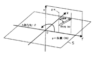
実際に、レーザ光線I1を照射して結晶化したp−Si膜5bについて、上記結晶の計測装置により、入射方向θ(入射角)を0°〜360°の範囲で変えてスペクトルの最大強度Imaxと、Imaxが得られる波長νmaxとを計測した。図2に入射角φ=0,1,2,3,4,5°におけるスペクトルの強度の入射方向θ依存性を示し、図3にスペクトルの最大強度Imaxが得られる波長νmaxの入射方向θ依存性を示す。入射方向θは、結晶の計測装置の光束31の方向で、結晶化後の試料5表面に平行でスキャン方向(試料台C8の移動方向X)と直交するY方向をθ=0°とした。
【0037】
ここで、角度θ、α、φは、次の通りである。
θ:図14に示すように、結晶の計測装置の光束31の試料5面(反射面)内のY方向に対する入射方向の角度
α:結晶の計測装置の光束31の計測用入射角
φ:結晶化するためのレーザ光線I1(ラインビーム)の入射角であり、試料5面(反射面)に対して垂直な入射面I2に存在する
【0038】
図2に示すように、φ=0°として結晶化させた場合は、光束31の入射方向θの如何によらずほぼ一定であり、結晶粒界が異方性を有していない。一方、φ=1〜5°として結晶化させた場合は、スペクトル強度は入射方向θ=0°、180°で最も大きく(スペクトルの最大強度Imax)、入射方向θ=90°、270°でも若干大きかつた。これは、等間隔で明確に生じている結晶粒界に光束31を照射するときに、多くの回折光32が明確かつ均質に生ずるためである。
【0039】
スペクトル最大強度が得られる波長は、図3に示すようであり、θ=90°、270°で最大となり、φが大きくなると波長は長くなつた。ここで、結晶粒の大きさDは、D=νmax/2・sinαから計算し、φとDとの関係を求めた。この式は、回折条件式から導かれる上記式:D=n・νmax/(sinα+sinβ)において、β=αとし、かつ、後記するようにn=1としたものである。その結果を図4(イ)(ロ)に黒丸印で示す。図4(イ)は、結晶化するためのレーザ光線I1の入射角φ=0〜5度の範囲で示し、図4(ロ)は、結晶化するためのレーザ光線I1の入射角φ=0〜50度の範囲で示す。但し、今回は、結晶の計測装置の光束31の計測用入射角α=50°に設定した。
【0040】
n=1とする理由について説明する。入射角φ=5°としてレーザ光線I1を照射して結晶化Si膜5bからなる試料5を作成すると共に計測装置を使用し、平行光31の結晶化Si膜5bへの照射方向を、照射した矩形をなすラインビーム(I1)の長軸方向(Y方向)つまり図8に示すθ=0°,90°とし、回折光32を得た。
【0041】
結晶化Si膜5bに、波長νが約380〜800nmの連続スペクトル光41を照射用光ファイバー42で伝送し、光ファイバー42の出射口から21mmの位置に配置した焦点距離f=21mmの凸レンズ44によつて平行光31となし、レンズ44からv=95mmの距離に保つた結晶化Si膜5bに、計測用入射角α=50°で平行光31を照射した。
【0042】
一方、結晶化Si膜5bの表面からの回折光32を先の凸レンズ44を透過させ、照射用光ファイバー42からu=0.2mmだけ平行に離れた位置にある受光用光ファイバー45に角度2δで入射させた。ここで、上述したようにuはvに比べて充分に小さい(0.2/95=0.002=2mrad)ため、回折光32の回折角βを照射した平行光31の入射角αと同じβ=α=50°とみなした。
【0043】
このような条件で分光器46を用いて測定した回折光32のスペクトルを、300〜800nmの波長範囲で図15に示す。図15(a)において実線iで示すθ=0度の回折光32のスペクトルは、波長500nm付近における鋭いピーク強度Imaxがあり、破線iiで示すθ=90度の回折光32のスペクトルは、波長585nm付近における鋭いピーク強度Imaxがある。他の波長域の連続スペクトルは、照射した平行光31が結晶化Si膜5bの表面で乱反射して受光用光ファイバー45に検出された成分である。参照のため、同様の測定をレーザ照射前のa−Si膜5aに対して行つた場合の測定値も同じグラフ上に薄い実線iiiで示した。なお、図15(b)は、図15(a)の実線i及び破線iiで示すp−Si膜5bのデータを薄い実線iiiで示すa−Si膜5aのデータで割算した結果を示すものであり、実線ivはθ=0度の結果を示し、破線vはθ=90度の結果を示す。図15(b)によつても、図15(a)と同様のピーク強度Imaxが知られる。
【0044】
この鋭いピーク強度Imaxを伴う結果から、結晶粒の配列・分布に適当な規則性があることが分かるので、次に結晶化Si膜5bの結晶粒の大きさD(Dx)を算出する。先ず、回折光32の次数は、分光器46での波長測定で500nm及び585nm(νmax)以外の波長に強いスペクトルが見られなかつたことから、これが1次であり、上記D=n・ν/(sinα+sinβ)なる式でn=1とする。
【0045】
なお、図15に示すように、平行光31の結晶化Si膜5bへの照射方向を、照射した矩形をなすラインビーム(I1)の長軸方向(Y方向)つまり図8に示すθ=0°とし、回折光32を得ることができるのみならず、平行光31の結晶化Si膜5bへの照射方向を、照射した矩形をなすラインビーム(I1)の短軸方向(X方向)つまり図8に示すθ=90°とし、回折光32を得ることもできる。従つて、入射面I2に直交する入射面I5より計測装置の平行光からなる光束31を入射し、計測装置の回折光32のスペクトルのピーク強度Imaxが図15(a)(b)に示す所定の大きさになるように、周期性構造を形成するためのレーザ光線I1の照射エネルギー密度を設定し、結晶粒の配列・分布の規則性を良好になしながら、その後の周期性構造を形成することができるのみならず、入射面I5に直交する入射面I2より計測装置の平行光からなる光束31を入射し、周期性構造を計測し、計測装置の回折光32のスペクトルのピーク強度Imaxが所定の大きさになるように、周期性構造を形成するためのレーザ光線I1の照射エネルギー密度を設定し、結晶粒の配列・分布の規則性を良好になしながら、その後の周期性構造を形成することができる。
【0046】
理論的には、入射角αと回折角βの値は異なつても問題ないが、レンズ44が1つで照射する平行光31及び回折光32の検出のための機構構成が簡素になるため、図13に示すような入射角αと回折角βとが事実上同じ角度になる測定装置が望ましい。
【0047】
次に、周期性構造をなす結晶の結晶粒界の対向する2辺が平行をなし、結晶粒の配列・分布に規則性が生ずる理由について検討する。φ=0,1,5°のときのSEM像(図5)を観察すると、φ=0°のときの結晶粒界の凸部は円弧状であり、φ=5°のときの結晶粒界の凸部は直線状である。また、φ=1°のときには、直線状の周期パターンの中に、φ=0°のときの円弧状パターンが部分的に見られた。なお、図5(c)は、図16と実質的に同じである。
【0048】
レーザ光線I1の入射角φ=0°でp−Si膜5bの結晶は試料5面内で等方的(図5(a)のφ=0°)であるが、φ>1°で入射面I2と直交する方向の結晶粒界で仕切られる結晶の周期性の間隔Dx(図5(b),(c)のφ=1,5°)が次第に大きくなる原因は、次のように推測される。
【0049】
光線が平坦状の試料5に入射したとき、試料5表面に微小な凹凸があると散乱光(ないし回折光)が発生し、球面波が形成される。入射光である平面波と、反射光である球面波とは互いに干渉し、電場強度分布は、レーザ光線I1の入射角φの方向に依存する。これについて図6を参照して説明する。
【0050】
エキシマレーザ光は、図6(b)に示すように特定の方向が偏光していないランダム偏光G7であるが、図6(a)に示すように偏光していないレーザ光線I1が入射角φで試料5の表面I7に入射すると、反射光I1’は、図6(c)に示すようにX方向を含む入射面I2と垂直なY方向の電場強度G5が強い光となる。従つて、入射面I2と平行なX方向に沿う干渉が強く起こり、試料5の温度は電場EとすればE2 に比例するため、干渉により強めあつた位置の温度が高くなり、図8に示す直交間隔Dyを有する結晶の周期構造I3が生ずる。
【0051】
次に、平面視でX方向から入射する平面波II1である入射光I1(レーザ光線)と反射光とがどのように干渉するかを模式図(図7)を参照して説明する。図7(a)に示すように時間tで入射光の平面波II1の一つの平面波面nが試料5に入射角φで入射すると、λ/c後に、1波長遅れた平面波面n+1が試料5面I7に到達し、反射光I1’の球面波II3の一つの波面n’は平面波面nより位相が1/2・λずれて発生するため、図7(b)に示すように時間t+3/2・λ/cで、平面波面n+1と球面波面n’とが強め合う。ここで、λは入射光I1の波長、cは光速である。
【0052】
更に時間T後に、図7(c)に示すように平面波面n+1と球面波面n−1’は、点pにおいて強め合う。このとき、平面波面n+1と表面I7との交点位置は、時間T後に、oからpに移動し、距離op=sとすれば、
s=cT/sinφ ・・・・・・・・(1)
【0053】
球面波面n−1’は、oからλ離れた位置より、光束cで表面I7を移動するため、
s=λ+cT ・・・・・・・・(2)
【0054】
(1)(2)より
T=(λ/c)(sinφ/(1−sinφ))・・(3)
【0055】
(3)を(1)に代入し、
s=λ/(1−sinφ) ・・・・・・・・(4)
この距離sを図8(b)に示す。
【0056】
従つて、図7の試料5面I7では、平面波II1である入射光I1と反射光I1’とが間隔sで電場強度Eが強め合う。また、この距離sは、多数の結晶粒の周期性の間隔(結晶粒の大きさ)Dに成長する。これにより、結晶の周期構造I9の周期性の間隔Dxが生ずる。図4(イ)(ロ)の結果に上記(4)式の結果を実線で示した。回折条件式から導かれる式:D=νmax/2・sinαによる結果を示す黒丸印とよく一致した。
【0057】
一方、結晶の周期構造I9と直交方向の結晶の周期構造I3の周期性の直交間隔Dyは、上記(4)式においてφ=0として、s=λにて求まる。この間隔Dyは、レーザ光線I1の電場強度Eが強め合つて生ずるが、電場強度G5が強いため、比較的明瞭に強く生ずる。この関係を実験結果に基づき表1に示す。レーザ光線I1からなる入射波があつて、図8に示すように試料5面I7の微小凹凸による回折波(反射光I1’)が反射波I1’x,I1’yとしてX方向及びY方向に生じるとき、反射光I1’の電場強度Eは、X方向の反射波I1’xで弱くY方向の反射波I1’yで強い。従つて、Si膜からなる試料5上の直交間隔Dyをなす周期性構造I3のX方向に伸びる(Y方向に繰り返す)結晶粒界は強く、間隔Dxをなす周期性構造I9のY方向に伸びる(X方向に繰り返す)結晶粒界は弱く生ずる。
【0058】
【表1】

しかして、前述したように入射面I2と平行なX方向に沿う干渉が強く起こり、試料5の温度は電場Eの二乗に比例し干渉により強めあつた位置の温度が高くなるため、図8(c)に示すように間隔Dyで結晶粒界が比較的強く生ずると同時に、図8(d)に示すように間隔Dxで結晶粒界が弱く生ずる。
【0060】
Si膜からなる試料5のレーザ光照射時の温度分布の周期は、上記(4)式のsに一致するため、入射角φに依存して大きくなる。φの大きさを調整することで、結晶の周期性の間隔(結晶粒の大きさ)Dxを調整することができる。図1の装置構成を基に、レーザ光2を入射面I2から入射光線I1として試料5面に入射させるとき、レーザ光線I1(ラインビーム)の短軸方向(X方向)の入射角φ=30°とすれば、λ=308nmの光を発生するエキシマレーザで、間隔:Dx×Dyが、0.308/(1−sin30°)×0.308/(1−sin0°)=0.62×0.31μmの方形の結晶粒が得られ、φ=50°とすれば、1.3×0.31μmの方形の結晶粒が得られる。
【0061】
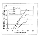
ところで、図9に示すように、レーザ光の試料5への照射回数が少ないときは結晶の計測装置によるスペクトルにピークがみられず、結晶に周期性が見られない。照射回数を増すことで、ピーク強度Imaxが大きくなり、320〜340mJ/cm2といつた最適な照射エネルギー密度による照射では、照射回数が18回以上でピーク強度Imaxが一定になる傾向がみられる。図9から分かるように、結晶に周期性を持たせるためには、試料5へのレーザ光の照射回数は複数回が必要であり、5回以上が好ましい。図10に示すように、レーザ光の試料5への照射回数を20回としたとき、計測装置の回折光32のスペクトルのピーク強度Imaxが所定の大きさになるように、周期性構造を形成するためのレーザ光の照射エネルギー密度(320〜340mJ/cm2)を設定し、p−Si膜5bにおける結晶粒の分布の規則性を良好になし得る。
【0062】
また、液晶パネルのTFTは、図11に示すソース・ドレインH5間を流れる電気移動度の大きさが、パネル全体で一定であることが望ましい。電気移動度は、p−Si結晶単体H3では単結晶Siの移動度に相当し、結晶粒界H4(突起38)の移動度は結晶単体H3(平坦部39)に比べて1〜2桁大きいといわれている。従つて、パネル全体に点在するTFTの電気移動度を一定にするためには、ソース・ドレインH5,H5間の結晶粒界H4の数が、パネル全体で一定であることが望ましい。
【0063】
ソース・ドレインH5電極の対向する辺H2の方向が一定であれば、ソース・ドレインH5間の距離Lに存在する結晶粒の数をパネル全体で均一にするためには、結晶の周期性の間隔D(Dy,Dx)が結晶粒の大きさに等しいから、L=m・D/cosω(mは整数)とすることが望ましい。ここで、ωは、多結晶シリコンからなるp−Si膜の作製後に形成させるソース・ドレインH5(不純物領域)の辺H2と結晶粒界H4(突起38)とのなす角度で、結晶粒界H4は結晶粒の周期構造I3,I9の方向と一致する。
【0064】
このように、結晶粒の大きさDはTFTのソース・ドレインH5間の距離Lに合わせて調整することが望ましいが、本方法によれば、レーザ光線の入射角φ(図8)を調整することで、容易にD(Dx)を調整することができる。すなわち、入射面I2と直交する方向の結晶粒界H4で仕切られる結晶の周期性の間隔Dxが、TFTのソース・ドレインH5の間隔Lに対して、L=m・Dx/cosω(mは整数)、ωはソース・ドレインH5の辺H2と結晶粒界H4とのなす角度となるように、レーザ光線I1の入射角φを調整することができる。
【0065】
また、レーザ光線の波長λを調整して、結晶粒の大きさD(直交間隔:Dy)を調整することができる。すなわち、入射面I2と平行な結晶粒界で仕切られる結晶の周期性の直交間隔Dyが、TFTのソース・ドレインH5の間隔Lに対して、L=m・Dy/cosω(mは整数)、ωはソース・ドレインH5の辺H2と結晶粒界H4とのなす角度となるように、レーザ光線I1の波長λを調整することができる。
【0066】
上記1実施の形態にあつては、図18に示すレーザ発振器3aで生じさせたレーザ光2を矩形のラインビームに整形し、このレーザ光線I1を図1に示す光学系の素子に導き、直線偏光でない1つのレーザ光線I1として試料5に照射したが、図1に示す光学系の素子は省略することが可能である。すなわち、図18に示す結晶粒の作成装置において、レーザ光線I1を入射角φを与えて1つの入射面I2から試料5に照射するように、入射角φを1度以上に設定できる光学系手段(図1に示す第3のミラーC4,試料台C8と同様のもの。)を備えさせればよい。例えば、図18に示す結晶粒の作成装置において、反射ミラー3c及び投影レンズ11を一体に傾動させるものを光学系手段とすることができる。
【0067】
更に、上記1実施の形態にあつては、直線偏光でない1つのレーザ光線I1を、ホモジナイザーA1,A2を通して入射角φを与えて1つの入射面I2から試料5に照射したが、同時に、直交入射面I5からも同様の直線偏光でない1つのレーザ光線を試料5に照射し、試料5を結晶化することも可能である。その際、入射面I2及び直交入射面I5から入射させる各1つのレーザ光線は、同じレーザ発振器3aで生じさせたレーザ光2をハーフミラーを通して分割させて用いることができる。
【0068】
【発明の効果】
以上の説明によつて理解されるように、本発明に係る結晶の周期性構造の形成方法及びその装置によれば、次の効果を奏することができる。
レーザ光を試料に照射する前に直線偏光にすることなく、レーザ光線を高出力のままで平坦な試料に照射させながら、試料上に結晶粒からなる良好な周期性構造を形成することが可能になる。結晶粒は、特定の方向に周期性を持ち、かつ、レーザ光の波長より大きくできる。その結果、良好な周期性を持たせた薄膜トランジスター等の製品を簡素な構造の装置によつて形成することが可能になる。
【0069】
請求項2,3,5,6によれば、試料の結晶の周期性の間隔つまり結晶粒の大きさ及び配列方向を知り、薄膜トランジスターのソース・ドレインを適正に配置することができる。特に、結晶粒界数の小さくなる配列方向にソース・ドレインを配置し、結晶粒界において電子の移動度が低下して薄膜トランジスターの電気的特性が悪化することを防止して、薄膜トランジスターの品質を向上させることが可能になる。
【0070】
また、請求項4,7のように計測装置を使用すれば、p−Si膜などの試料における結晶粒の配列ないし分布の規則性の評価を簡易に行ない、ひいては、良好なエネルギー密度のレーザ光を試料に照射して、均一かつ適正な規則性を有する結晶を試料の全面に形成することができる。加えて、計測装置の使用により、レーザ光を照射して試料を結晶化させながら、レーザ光のエネルギー密度を制御し、予め決定した結晶化に適する回折光のスペクトル強度及び波長を得ることができる。これにより、レーザ光を照射して試料を結晶化させながら、均一かつ適正な規則性を有する結晶を試料の全面に無駄なく形成することができる。
【図面の簡単な説明】
【図1】 本発明の1実施の形態に係る結晶の周期性構造の形成装置の要部を示す正面図。
【図2】 同じくレーザ光線の入射角を変化させて結晶化させた試料に対し、計測装置の光束の入射角を変化させて得た回折光のスペクトルの最大強度(任意単位)特性を示す線図。
【図3】 同じくレーザ光線の入射角を変化させて結晶化させた試料に対し、計測装置の光束の入射角を変化させて得た回折光のスペクトル最大強度が得られる波長特性を示す線図。
【図4】 同じくレーザ光線の入射角−結晶粒の大きさ特性を示す線図であり、図4(イ)は、結晶化するためのレーザ光線I1の入射角φ=0〜5度の範囲で示し、図4(ロ)は、結晶化するためのレーザ光線I1の入射角φ=0〜50度の範囲で示す。
【図5】 同じくレーザ光線の入射角を変えたときのp−Si膜のSEM写真を示し、(a)は入射角:φ=0°、(b)は入射角:φ=1°、(c)は入射角:φ=5°を示す。
【図6】 同じくレーザ光線を所定入射角で試料の表面に入射するときの説明図であり、(a)はレーザ光線及び試料を示す説明図、(b)は入射光の電場強度分布を示す説明図、(c)は反射光の電場強度分布を示す説明図。
【図7】 同じく入射光と反射光との干渉を示す模式図であり、(a)は時間tで入射光の平面波が試料に入射角φで入射するときを示し、(b)は時間t+3/2・λ/cで平面波面n+1と球面波面n’とが強め合う状態を示し、(c)は時間t+3/2・λ/c+Tで平面波面n+1と球面波面n−1’とが強め合う状態を示す図。
【図8】 同じくレーザ光線を所定入射角で試料の表面に入射するときの説明図であり、(a)はレーザ光線及び試料を示す説明図、(b)は図7(c)と同様に平面波面n+1と球面波面n’,n−1’とが強め合う間隔を示し、(c)はX方向に伸びる結晶粒界で仕切られた周期構造の結晶粒界による直交間隔を示し、(d)はY方向に存在する直交入射面と平行な結晶粒界による間隔を示す図。
【図9】 同じくレーザ光線の照射回数−評価装置のスペクトル最大強度(任意単位)特性を示す線図。
【図10】 同じくレーザ光線のエネルギー密度−評価装置のスペクトル最大強度(任意単位)特性を示す線図。
【図11】 同じくソース・ドレインを形成した液晶パネルのTFTを示す概略図。
【図12】 同じく結晶評価装置の原理を示す正面図。
【図13】 同じく結晶評価装置を示す正面図。
【図14】 同じく結晶評価装置の入射方向を変化させて回折光のスペクトルを得るための説明図。
【図15】 同じく評価装置の回折光の波長−強度(任意単位)特性を示す線図であり、図14(a)は測定値の線図、図14(b)はθ=0度及び90度としたp−Si膜の測定値をa−Si膜のデータで割算した結果を示す。
【図16】 同じくレーザ光の入射角を5°としたときの結晶のSEM写真を示す図。
【図17】 従来のレーザ光の入射角を0°としたときの結晶のSEM写真を示す図。
【図18】 従来の結晶粒の作成装置を示し、(a)は正面図、(b)は右側面図。
【図19】 従来の結晶化Si膜の作成装置に組み込むホモジナイザーを示す斜視図。
【符号の説明】
3a:レーザ発振器、5:試料、5a:a−Si膜、5b:p−Si膜、31:光束、32:回折光、35:正反射光、41:連続光(光源)、42:照射用光ファイバー(光源)、44:レンズ、45:受光用光ファイバー、46:分光器、47:表示装置、A1,A2:ホモジナイザー、C4:第3のミラー(光学系手段)、C8:試料台(光学系手段)、D:間隔(結晶粒の大きさ)、Dx:間隔、Dy:直交間隔、H2:ソース・ドレインの辺、H4:結晶粒界、H5:薄膜トランジスターのソース・ドレイン、I1:レーザ光線、I2:入射面、I5:直交入射面、L:ソース・ドレインの間隔、zn:法線、α:計測用入射角、β:回折角、θ:入射方向、λ:レーザ光線の波長、ν:回折光のスペクトル波長、φ:入射角。[0001]
BACKGROUND OF THE INVENTION
The present invention relates to a method and apparatus for forming a periodic structure of a crystal, and a periodic structure of a crystal. More specifically, in a polycrystalline semiconductor film used for a liquid crystal display device or the like, a periodic structure composed of crystal grains is formed on a sample. The present invention relates to a forming method and an apparatus thereof, and a periodic structure of a crystal.
[0002]
[Prior art]
1. Crystallization by line beam
For example, a method of irradiating a sample with a laser beam composed of a line beam is known when manufacturing crystallized silicon of a thin film transistor used in a liquid crystal display device. As shown in FIG. 18, the
[0003]
The
[0004]
Here, since the pulse width (light emission time) of the
[0005]
The crystallinity of the p-
[0006]
The reason why crystal grains having the same wavelength as that of the
[0007]
2. Formation of periodic crystals by linearly polarized light
It has been attempted to form crystal grains larger than the wavelength of the laser light by obliquely incident linearly polarized laser light on the a-Si film (Horita, “Alignment of grain boundary in a Si film crystallized by a linear According to this method, due to the interference between the incident plane wave and the reflected plane wave, the periodic structure in the direction perpendicular to the incident plane has an incident angle: When φ, it can be formed at intervals of D = λ / (1-sinφ).
[0008]
3. Formation of periodic crystals by two-beam interference.
As a means for increasing the crystal grain size and providing periodicity, as described in JP-A-10-256152, a standing wave is formed at a predetermined position on the surface of the a-Si film by using two laser beams. There is a method of performing melting by irradiating from the front and back at a certain incident angle, generating a heat density distribution having the same period as the standing wave at the predetermined position. This method forms a standing wave by causing laser light to interfere with the surface of the a-Si film. The period of the standing wave is λ ′ / (2 sin θ ′) where the wavelength of the laser beam is λ ′ and the incident angle is θ ′. Therefore, the period of the standing wave, that is, the period of the heat density distribution formed on the semiconductor surface can be controlled with high accuracy by adjusting the incident angle with respect to a certain wavelength of the laser beam. . This method is, for example, a two-beam interference method disclosed in Japanese Patent Laid-Open No. 10-39125, and is used for manufacturing a diffraction grating.
[0009]
[Problems to be solved by the invention]
1. Problems of crystallization by line beam
The size of a crystal produced by a conventional line beam method using excimer laser light is approximately equal to the wavelength of the laser light, and crystals larger than the wavelength cannot be produced uniformly. Further, the crystal grains did not have periodicity in a specific direction as can be seen from FIG.
[0010]
2. Problems of periodic crystal formation by linearly polarized light
An excimer laser is used as a laser that emits light in the ultraviolet region having a high absorption power to the a-Si film and can obtain high-power pulsed light. Excimer laser light is random polarized light having no specific polarization. In order to make the excimer laser beam linearly polarized, it is necessary to use a polarizing plate or the like, so that the output is significantly reduced. For this reason, it is desired to form a periodic structure of a crystal on the sample by irradiating the sample with a laser beam that is not linearly polarized light.
[0011]
3. Problems of crystal formation with periodicity due to two-beam interference
Two laser beams from one incident surface must be irradiated from the front and back at an incident angle such that a standing wave is formed at a predetermined position on the surface of the a-Si film, and the configuration of the optical system becomes complicated. . In particular, two laser beams are incident from one incident surface, and the period of the standing wave is λ ′ / (2 sin θ ′) where the wavelength of the laser beam is λ ′ and the incident angle is θ ′. Not only is the angle of incidence θ ′ for obtaining a standing wave period larger than λ ′ limited, but the structure becomes complicated. Further, for example, when a crystal grain having a size of 1 μm is formed by two-beam interference using an excimer laser beam (wavelength 308 nm), the incident angle θ ′ = arcsin (λ ′ / 2 · 1 μm) = 8 of two rays. At 9 °, the numerical aperture NA = n · sin θ ′ = n · 0.154. At this time, DOF = K · λ / NA2= K ′ · 13 μm. The apparatus of FIG. 18 using the above-described line beam has NA = 0.05 by the
[0012]
4). When a p-Si film is used for a thin film transistor (hereinafter referred to as “TFT”), the TFT characteristics depend on the number of crystal grain boundaries between the source and the drain, and the smaller the grain boundary number, the better the electrical characteristics. Therefore, in order to make the TFT characteristics of the entire glass substrate uniform, it is desirable that the crystal grains are large and uniform. If the direction of the periodicity of the crystal is known, the source / drain can be arranged so that the number of crystal grain boundaries between the source / drain is reduced.
[0013]
[Means for Solving the Problems]
The present invention has been made in view of such a conventional technical problem, and the configuration thereof is as follows.
The invention of
One laser beam I1 that is not linearly polarized light is incident on the
Claim2The invention ofA method of irradiating a
One laser beam I1 that is not linearly polarized light is incident on the
The
Claim3The invention ofA method of irradiating a
One laser beam I1 that is not linearly polarized light is incident on the
The
Claim4The invention ofA method of irradiating a
One laser beam I1 that is not linearly polarized light is incident on the
The periodic structure of the formed crystal is a light beam 31 composed of parallel light of the measuring device from the incident surface (I5 or I2) orthogonal to the incident surface I2 of the
Light sources 41 and 42 for causing the measurement device to inject a light beam 31 composed of parallel light having a normal line zn from the plane of the
The ranges of the incident angle α and the diffraction angle β for measurement are both limited to a range of 0 ° or more and 90 ° or less to obtain the diffracted light 32 that does not include the specularly reflected light 35, and from the spectrum peak intensity Imax of the diffracted light 32. A method for forming a periodic structure of crystals, characterized by evaluating the regularity of the distribution of crystal grains in
Claim5The invention of is a single laser beam I1, which is not linearly polarized,
Homogenizers A1, A2 for shaping the laser beam I1,
An optical system means (C4, C8) which irradiates the
And a sample stage C8 on which the
Crystal periodic structure forming apparatus for forming a crystal periodic structure on a
The laser beam I1 is an excimer laser that generates ultraviolet rays, the
The periodic interval Dx of the crystal partitioned by the crystal grain boundary H4 in the direction orthogonal to the incident surface I2 is L = m · Dx / cos ω (m is an integer) with respect to the interval L between the source and drain H5 of the thin film transistor. ), The magnitude of the incident angle φ of the laser beam I1 is adjusted so that ω is an angle formed between the side H2 of the source / drain H5 and the grain boundary H4.An apparatus for forming a periodic structure of a crystal.
Claim6According to the present invention, the periodic orthogonal distance Dy of the crystal partitioned by the crystal grain boundary parallel to the incident surface I2 is L = m · Dy / cos ω (m) with respect to the distance L between the source and drain H5 of the thin film transistor. The wavelength λ of the laser beam I1 is adjusted so that ω is an angle formed by the side H2 of the source / drain H5 and the grain boundary H4.5Of the periodic structure of crystalsapparatusIt is.
Claim7According to the present invention, the periodic structure of the formed crystal is reflected from the incident surface I2 of the
Light sources 41 and 42 for causing the measurement device to inject a light beam 31 composed of parallel light having a normal line zn from the plane of the
The ranges of the incident angle α and the diffraction angle β for measurement are both limited to a range of 0 ° or more and 90 ° or less to obtain the diffracted light 32 that does not include the specularly reflected light 35, and from the spectrum peak intensity Imax of the diffracted light 32. The regularity of the distribution of crystal grains in the
[0014]
The outline of the present invention will be described.
The inventors use the apparatus shown in FIG. 18 to project the mirror 3c and the projection so that the incident angle (φ) of the laser beam I1 made of a line beam to the
[0015]
An investigation was conducted to determine the cause of the periodicity of such crystals, and this periodic structure was generated by the interference between the incident wave and the reflected wave, and the laser beam was not polarized in a specific direction. When I1 is reflected by the
[0016]
The present invention will be further described with reference to FIG.
(1) As shown in FIG. 8 (a), one laser beam I1 that is not one linearly polarized light is incident on a
[0017]
(2) The orthogonal interval Dy due to the crystal grain boundary of the periodic structure I3 of the crystal is present in the Y direction and coincides with the wavelength λ of the laser beam I1 incident from the incident surface I2. The interval Dx of the periodic structure I9 in the direction orthogonal to the interval Dy of the periodic structure I3 of the crystal, that is, the interval Dx due to the crystal grain boundary parallel to the orthogonal incident surface I5 existing in the Y direction orthogonal to the incident surface I2 is shown in FIG. It is obtained as s shown in b) and can be controlled by the incident angle φ of the laser beam I1 incident from the incident surface I2. 8A and 8B, N is a vertical line standing on the surface I7 of the
[0018]
(3) By setting φ> 1 °, the electric field intensity E in the Y direction of the reflected wave is increased, and a crystal having periodicity in the two directions of the X axis and the Y axis can be formed. At this time, the crystal grain boundary of one crystal of the periodic structure forms a rectangle in which two opposing sides are parallel. The parallelism of the periodic structure I3 is obtained strongly and clearly, and the parallelism of the periodic structure I9 is obtained weakly.
[0019]
(4) The periodic interval Dx of the crystal due to the irradiation of the laser beam I1 was Dx = λ / (1-sinφ). This periodic interval Dx corresponds to the size of the crystal grain, and becomes larger than the wavelength λ of the laser beam I1 to be irradiated by setting it in the range of 0 ° <φ> 90 °.
[0020]
(5) The
[0021]
(6) The actually used laser beam I1 which is not linearly polarized light is an excimer laser that generates light having a wavelength of λ = 308 nm. The
[0022]
The periodic intervals Dx and Dy of the crystal grains coincide with the size of the crystal grains if the crystals are sufficiently grown by recrystallization by multiple irradiations of the laser beam I1.
[0023]
The method and apparatus of the present invention are optimal for crystallization of a-Si films, but can also be applied to the formation of diffraction gratings used in semiconductor lasers and the like, and the types of samples irradiated with laser light are limited. Not.
[0024]
DETAILED DESCRIPTION OF THE INVENTION
In the following, one embodiment of the present invention will be described with the same reference numerals assigned to the same functional parts as in the conventional example.
First, the
[0025]
The crystal grains of the p-
[0026]
A crystal measurement device (evaluation device) for evaluating the periodicity of crystal grains of the p-
[0027]
If the detection of the diffracted light 32 is performed in the direction of the specularly reflected light 35 (reflection angle: -α) or in the vicinity thereof, the spectral intensity of the specularly reflected light 35 is much higher than the spectral intensity of the diffracted light 32. It is difficult to separate only the spectral component of the diffracted light 32 from the two superimposed spectral components. Therefore, in order to detect only the spectrum of the diffracted light 32 with high accuracy, both α and β are limited to 0 ° or more and 90 ° or less, and the diffracted light 32 not including the
[0028]
Accordingly, in the front view shown in FIG. 12, when the light beam 31 made of parallel light is incident at the measurement incident angle α, the diffraction is performed on the same side as the light beam 31 with respect to the normal line zn from the plane of the p-
[0029]
In this way, the light beam 31 having a continuous spectrum is incident, and the diffracted light 32 generated at several protrusions 38 (several tens of nm) at the crystal grain boundary of the p-
[0030]
That is, if the spectral intensity (peak intensity Imax) and wavelength of the diffracted light 32 optimum for crystallization are determined in advance within the irradiation energy density range in which the laser beam (2) can be used, the
[0031]
Alternatively, the crystal grain size Dx can be obtained, and the
[0032]
Therefore, as shown in FIG. 13, the measuring apparatus for evaluating the periodic structure of the crystal has a normal line from the plane of the p-
[0033]
The light source (41, 42) has continuous light 41 obtained by a halogen lamp and an irradiation optical fiber 42 as shown in FIG. 13, and continuous light 41 having a predetermined wavelength (ν = 380 to 800 nm) is used for irradiation. The light guided to the optical fiber 42 and emitted from the tip of the optical fiber 42 is converted into a light beam 31 by the
[0034]
Note that the diffracted light 32 is incident at an angle 2δ on the light receiving optical fiber 45 located parallel to the irradiation optical fiber 42 by u = 0.2 mm, where u is v (the
[0035]
Further, in the p-
[0036]
Actually, for the p-
[0037]
Here, the angles θ, α, and φ are as follows.
θ: As shown in FIG. 14, the angle of the incident direction with respect to the Y direction in the
α: Incident angle for measuring the luminous flux 31 of the crystal measuring device
φ: incident angle of laser beam I1 (line beam) for crystallization, present on incident surface I2 perpendicular to sample 5 surface (reflection surface)
[0038]
As shown in FIG. 2, when crystallization is performed with φ = 0 °, the crystal grain boundary is almost constant regardless of the incident direction θ of the light beam 31, and the crystal grain boundary has no anisotropy. On the other hand, when crystallization is performed at φ = 1 to 5 °, the spectral intensity is the highest in the incident direction θ = 0 ° and 180 ° (maximum intensity Imax of the spectrum), and slightly in the incident direction θ = 90 ° and 270 °. It was big. This is because a lot of diffracted light 32 is clearly and uniformly generated when the light flux 31 is irradiated to the crystal grain boundaries clearly generated at equal intervals.
[0039]
The wavelength at which the maximum spectrum intensity can be obtained is as shown in FIG. 3, and becomes maximum at θ = 90 ° and 270 °, and the wavelength becomes longer as φ increases. Here, the crystal grain size D was calculated from D = νmax / 2 · sin α, and the relationship between φ and D was obtained. In this equation, D = n · νmax / (sin α + sin β) derived from the diffraction condition equation, β = α and n = 1 as described later. The results are shown by black circles in FIGS. 4A shows the incident angle φ of the laser beam I1 for crystallization in the range of 0 to 5 degrees, and FIG. 4B shows the incident angle φ = 0 of the laser beam I1 for crystallization. Shown in the range of -50 degrees. However, this time, the incident angle α for measurement of the luminous flux 31 of the crystal measuring device was set to 50 °.
[0040]
The reason why n = 1 is described. The
[0041]
A continuous spectrum light 41 having a wavelength ν of about 380 to 800 nm is transmitted to the
[0042]
On the other hand, the diffracted light 32 from the surface of the
[0043]
The spectrum of the diffracted light 32 measured using the
[0044]
From the result with this sharp peak intensity Imax, it can be seen that there is an appropriate regularity in the arrangement and distribution of crystal grains. Next, the crystal grain size D (Dx) of the
[0045]
As shown in FIG. 15, the irradiation direction of the parallel light 31 onto the
[0046]
Theoretically, there is no problem even if the values of the incident angle α and the diffraction angle β are different. However, since the mechanism configuration for detecting the parallel light 31 and the diffracted light 32 irradiated by one
[0047]
Next, the reason why two opposing sides of a crystal grain boundary of a crystal having a periodic structure are parallel and regularity occurs in the arrangement and distribution of crystal grains will be examined. When the SEM image at φ = 0, 1, 5 ° (FIG. 5) is observed, the convex portion of the crystal grain boundary at φ = 0 ° is arcuate, and the crystal grain boundary at φ = 5 ° The convex part of is linear. Further, when φ = 1 °, an arc-like pattern when φ = 0 ° was partially seen in the linear periodic pattern. FIG. 5C is substantially the same as FIG.
[0048]
The incident angle φ of the laser beam I1 is 0 °, and the crystal of the p-
[0049]
When a light beam is incident on the
[0050]
The excimer laser beam is random polarization G7 in which a specific direction is not polarized as shown in FIG. 6B, but the unpolarized laser beam I1 is incident at an incident angle φ as shown in FIG. 6A. When incident on the surface I7 of the
[0051]
Next, how the incident light I1 (laser beam) that is the plane wave II1 incident from the X direction in plan view interferes with the reflected light will be described with reference to a schematic diagram (FIG. 7). As shown in FIG. 7A, when one plane wavefront n of the plane wave II1 of the incident light is incident on the
[0052]
Further, after time T, as shown in FIG. 7C, the plane wavefront n + 1 and the spherical wavefront n-1 'strengthen each other at the point p. At this time, the intersection position of the plane wavefront n + 1 and the surface I7 moves from o to p after time T, and if the distance op = s,
s = cT / sinφ (1)
[0053]
Since the spherical wavefront n-1 'moves on the surface I7 with the light beam c from a position away from λ by λ,
s = λ + cT (2)
[0054]
(1) From (2)
T = (λ / c) (sin φ / (1-sin φ)) (3)
[0055]
Substituting (3) into (1),
s = λ / (1-sinφ) (4)
This distance s is shown in FIG.
[0056]
Therefore, on the
[0057]
On the other hand, the periodic orthogonal interval Dy between the periodic structure I9 of the crystal and the periodic structure I3 of the crystal in the orthogonal direction can be obtained by s = λ with φ = 0 in the above equation (4). This interval Dy is generated when the electric field intensity E of the laser beam I1 is strengthened, but is relatively clearly generated because the electric field intensity G5 is strong. This relationship is shown in Table 1 based on the experimental results. As shown in FIG. 8, a diffracted wave (reflected light I1 ′) due to minute unevenness on the
[0058]
[Table 1]
Therefore, as described above, interference along the X direction parallel to the incident surface I2 occurs strongly, and the temperature of the
[0060]
The period of the temperature distribution at the time of laser beam irradiation of the
[0061]
By the way, as shown in FIG. 9, when the number of times the laser beam is applied to the
[0062]
Further, in the TFT of the liquid crystal panel, it is desirable that the electric mobility flowing between the source and drain H5 shown in FIG. 11 is constant throughout the panel. The electric mobility corresponds to the mobility of single crystal Si in the p-Si crystal simple substance H3, and the mobility of the crystal grain boundary H4 (projection 38) is 1 to 2 orders of magnitude higher than that of the crystal simple substance H3 (flat portion 39). It is said that. Therefore, in order to make the electric mobility of TFTs scattered throughout the panel constant, it is desirable that the number of crystal grain boundaries H4 between the source / drain H5 and H5 is constant throughout the panel.
[0063]
If the direction of the opposite side H2 of the source / drain H5 electrode is constant, in order to make the number of crystal grains existing at the distance L between the source / drain H5 uniform throughout the panel, the periodic interval of the crystals Since D (Dy, Dx) is equal to the size of the crystal grains, it is desirable to set L = m · D / cos ω (m is an integer). Here, ω is an angle formed between the side H2 of the source / drain H5 (impurity region) formed after the preparation of the p-Si film made of polycrystalline silicon and the crystal grain boundary H4 (projection 38), and the crystal grain boundary H4. Corresponds to the direction of the periodic structure I3, I9 of the crystal grains.
[0064]
As described above, it is desirable to adjust the crystal grain size D according to the distance L between the source and drain H5 of the TFT. However, according to this method, the incident angle φ of the laser beam (FIG. 8) is adjusted. Thus, D (Dx) can be easily adjusted. That is, the periodic interval Dx of the crystal partitioned by the crystal grain boundary H4 in the direction orthogonal to the incident surface I2 is L = m · Dx / cos ω (m is an integer) with respect to the interval L between the source and drain H5 of the TFT. ), The incident angle φ of the laser beam I1 can be adjusted so that ω is an angle formed by the side H2 of the source / drain H5 and the crystal grain boundary H4.
[0065]
Further, the crystal grain size D (orthogonal spacing: Dy) can be adjusted by adjusting the wavelength λ of the laser beam. That is, the periodic orthogonal distance Dy of the crystal partitioned by the crystal grain boundary parallel to the incident surface I2 is L = m · Dy / cosω (m is an integer) with respect to the distance L between the source and drain H5 of the TFT, The wavelength λ of the laser beam I1 can be adjusted so that ω is an angle formed by the side H2 of the source / drain H5 and the crystal grain boundary H4.
[0066]
In the first embodiment, the
[0067]
Further, in the first embodiment, one laser beam I1 which is not linearly polarized light is irradiated to the
[0068]
【The invention's effect】
As can be understood from the above description, according to the method and apparatus for forming a periodic structure of a crystal according to the present invention, the following effects can be obtained.
It is possible to form a good periodic structure consisting of crystal grains on a sample while irradiating a flat sample while keeping the laser beam at a high output without irradiating the sample with linearly polarized light. become. The crystal grains have periodicity in a specific direction and can be larger than the wavelength of the laser beam. As a result, a product such as a thin film transistor having good periodicity can be formed by a device having a simple structure.
[0069]
Claim2, 3, 5, 6According to this, it is possible to know the periodic interval of the crystal of the sample, that is, the size and arrangement direction of the crystal grains, and to appropriately arrange the source and drain of the thin film transistor. In particular, the source and drain are arranged in the direction of arrangement in which the number of crystal grain boundaries is small, and the quality of the thin film transistor is prevented by preventing the mobility of electrons from decreasing at the crystal grain boundary and degrading the electrical characteristics of the thin film transistor. It becomes possible to improve.
[0070]
Claims4,7If the measurement device is used as described above, the regularity of the arrangement or distribution of crystal grains in a sample such as a p-Si film is simply evaluated, and as a result, the sample is irradiated with laser light having a good energy density, Crystals having uniform and appropriate regularity can be formed on the entire surface of the sample. In addition, by using a measuring device, the energy density of the laser beam can be controlled while irradiating the laser beam to crystallize the sample, and the spectral intensity and wavelength of diffracted light suitable for crystallization determined in advance can be obtained. . Thereby, a crystal having uniform and appropriate regularity can be formed on the entire surface of the sample without waste while crystallizing the sample by laser irradiation.
[Brief description of the drawings]
FIG. 1 is a front view showing a main part of an apparatus for forming a periodic structure of crystals according to an embodiment of the present invention.
FIG. 2 is a line showing the maximum intensity (arbitrary unit) characteristic of the spectrum of diffracted light obtained by changing the incident angle of the light beam of the measuring device with respect to a sample crystallized by changing the incident angle of the laser beam. Figure.
FIG. 3 is a diagram showing a wavelength characteristic for obtaining the maximum spectral intensity of diffracted light obtained by changing the incident angle of the light beam of the measuring device with respect to a sample crystallized by changing the incident angle of the laser beam. .
4 is a diagram showing the incident angle of the laser beam and the size characteristic of the crystal grain, and FIG. 4A shows the range of the incident angle φ = 0 to 5 degrees of the laser beam I1 for crystallization. FIG. 4B shows the incident angle φ of the laser beam I1 for crystallization in the range of 0 to 50 degrees.
5 shows SEM photographs of the p-Si film when the incident angle of the laser beam is similarly changed. (A) is an incident angle: φ = 0 °, (b) is an incident angle: φ = 1 °, ( c) shows an incident angle: φ = 5 °.
FIG. 6 is also an explanatory diagram when a laser beam is incident on the surface of the sample at a predetermined incident angle, (a) is an explanatory diagram showing the laser beam and the sample, and (b) is an electric field intensity distribution of the incident light. Explanatory drawing, (c) is explanatory drawing which shows electric field intensity distribution of reflected light.
FIG. 7 is a schematic diagram showing the interference between incident light and reflected light, where (a) shows a time when a plane wave of incident light is incident on a sample at an incident angle φ, and (b) shows
FIG. 8 is also an explanatory diagram when a laser beam is incident on the surface of the sample at a predetermined incident angle, (a) is an explanatory diagram showing the laser beam and the sample, and (b) is the same as FIG. 7 (c). The plane wavefront n + 1 and the spherical wavefronts n ′ and n−1 ′ are shown to be intensified intervals, (c) is the orthogonal interval due to the crystal grain boundaries of a periodic structure partitioned by crystal grain boundaries extending in the X direction, and (d ) Is a diagram showing an interval between crystal grain boundaries parallel to the orthogonal incident surface existing in the Y direction.
FIG. 9 is a diagram illustrating the number of times of laser beam irradiation and the spectral maximum intensity (arbitrary unit) characteristics of the evaluation apparatus.
FIG. 10 is a diagram similarly showing the energy density of a laser beam-spectrum maximum intensity (arbitrary unit) characteristics of the evaluation apparatus.
FIG. 11 is a schematic view showing a TFT of a liquid crystal panel in which a source / drain is also formed.
FIG. 12 is a front view showing the principle of the crystal evaluation apparatus.
FIG. 13 is a front view showing the same crystal evaluation apparatus.
FIG. 14 is an explanatory diagram for obtaining a spectrum of diffracted light by changing the incident direction of the crystal evaluation apparatus.
15 is a diagram showing the wavelength-intensity (arbitrary unit) characteristics of diffracted light of the evaluation apparatus, FIG. 14A is a diagram of measured values, and FIG. 14B is θ = 0 degrees and 90; The result of dividing the measured value of the p-Si film by the data of the a-Si film is shown.
FIG. 16 is a view showing an SEM photograph of a crystal when the incident angle of laser light is 5 °.
FIG. 17 is a view showing a SEM photograph of a crystal when the incident angle of a conventional laser beam is 0 °.
18A and 18B show a conventional crystal grain creation device, where FIG. 18A is a front view, and FIG. 18B is a right side view.
FIG. 19 is a perspective view showing a homogenizer incorporated in a conventional crystallized Si film forming apparatus.
[Explanation of symbols]
3a: laser oscillator, 5: sample, 5a: a-Si film, 5b: p-Si film, 31: light beam, 32: diffracted light, 35: specularly reflected light, 41: continuous light (light source), 42: for irradiation Optical fiber (light source), 44: lens, 45: optical fiber for light reception, 46: spectroscope, 47: display device, A1, A2: homogenizer, C4: third mirror (optical system means), C8: sample stage (optical system) Means), D: spacing (crystal grain size), Dx: spacing, Dy: orthogonal spacing, H2: source / drain sides, H4: crystal grain boundary, H5: source / drain of thin film transistor, I1: laser beam , I2: incidence plane, I5: orthogonal incidence plane, L: source / drain spacing, zn: normal, α: measurement incidence angle, β: diffraction angle, θ: incidence direction, λ: wavelength of laser beam, ν : Spectral wavelength of diffracted light, φ: incident angle.
Claims (7)
直線偏光でない1つのレーザ光線(I1)を、入射角(φ)>1°で1つの入射面(I2)から試料(5)に入射させることで、該レーザ光線(I1)の入射面(I2)に平行な結晶粒界で仕切られて直交間隔(Dy)をなす周期性構造を形成すると共に、前記入射面(I2)と直交する方向の結晶粒界で仕切られる結晶の周期性の間隔(Dx)を、レーザ光線(I1)の入射角(φ)の大きさによつてコントロールすることを特徴とする結晶の周期性構造の形成方法。A method of irradiating a flat sample (5) with a laser beam and forming a periodic structure composed of crystal grains on the sample (5),
By making one laser beam (I1) that is not linearly polarized light enter the sample (5) from one incident surface (I2) at an incident angle (φ)> 1 °, the incident surface (I2) of the laser beam (I1) ) To form a periodic structure which is partitioned by crystal grain boundaries parallel to each other to form orthogonal intervals (Dy), and the periodic interval of crystals partitioned by crystal grain boundaries in a direction orthogonal to the incident surface (I2) ( Dx) is controlled by the magnitude of the incident angle (φ) of the laser beam (I1) .
直線偏光でない1つのレーザ光線(I1)を、入射角(φ)>1°で1つの入射面(I2)から試料(5)に入射させることで、該レーザ光線(I1)の入射面(I2)に平行な結晶粒界で仕切られて直交間隔(Dy)をなす周期性構造を形成すると共に、
前記試料(5)は薄膜トランジスターであり、前記入射面(I2)と直交する方向の結晶粒界で仕切られる結晶の周期性の間隔Dxが、薄膜トランジスターのソース・ドレイン(H5)の間隔Lに対して、L=m・Dx/cosω(mは整数)、ωはソース・ドレイン(H5)の辺(H2)と結晶粒界(H4)とのなす角度となるように、レーザ光線(I1)の入射角(φ)を調整することを特徴とする結晶の周期性構造の形成方法。 A method of irradiating a flat sample (5) with a laser beam and forming a periodic structure composed of crystal grains on the sample (5),
By making one laser beam (I1) that is not linearly polarized light enter the sample (5) from one incident surface (I2) at an incident angle (φ)> 1 °, the incident surface (I2) of the laser beam (I1) ) To form a periodic structure that is partitioned by crystal grain boundaries parallel to each other to form orthogonal intervals (Dy),
The sample (5) is a thin film transistor, and the periodic interval Dx of the crystal partitioned by the crystal grain boundary in the direction orthogonal to the incident surface (I2) is the distance L between the source and drain (H5) of the thin film transistor. On the other hand, L = m · Dx / cos ω (m is an integer), and ω is an angle formed by the side (H2) of the source / drain (H5) and the crystal grain boundary (H4). A method for forming a periodic structure of a crystal, wherein the incident angle (φ) of the crystal is adjusted.
直線偏光でない1つのレーザ光線(I1)を、入射角(φ)>1°で1つの入射面(I2)から試料(5)に入射させることで、該レーザ光線(I1)の入射面(I2)に平行な結晶粒界で仕切られて直交間隔(Dy)をなす周期性構造を形成すると共に、
前記試料(5)は薄膜トランジスターであり、結晶の周期性の直交間隔Dyが、薄膜トランジスターのソース・ドレイン(H5)の間隔Lに対して、L=m・Dy/cosω(mは整数)、ωはソース・ドレイン(H5)の辺(H2)と結晶粒界(H4)とのなす角度となるように、レーザ光線(I1)の波長(λ)を調整することを特徴とする結晶の周期性構造の形成方法。 A method of irradiating a flat sample (5) with a laser beam and forming a periodic structure composed of crystal grains on the sample (5),
By making one laser beam (I1) that is not linearly polarized light enter the sample (5) from one incident surface (I2) at an incident angle (φ)> 1 °, the incident surface (I2) of the laser beam (I1) ) To form a periodic structure that is partitioned by crystal grain boundaries parallel to each other to form orthogonal intervals (Dy),
The sample (5) is a thin film transistor, and the orthogonal interval Dy of the periodicity of the crystal is L = m · Dy / cos ω (m is an integer) with respect to the distance L between the source and drain (H5) of the thin film transistor, The period of the crystal is characterized in that the wavelength (λ) of the laser beam (I1) is adjusted so that ω is an angle formed between the side (H2) of the source / drain (H5) and the crystal grain boundary (H4). Of forming the structure.
直線偏光でない1つのレーザ光線(I1)を、入射角(φ)>1°で1つの入射面(I2)から試料(5)に入射させることで、該レーザ光線(I1)の入射面(I2)に平行な結晶粒界で仕切られて直交間隔(Dy)をなす周期性構造を形成すると共に、
形成した結晶の周期性構造を、試料(5)の入射面(I2)又は入射面(I2)と直交する方向の直交入射面(I5)に対して直交する入射面(I5又はI2)より計測装置の平行光からなる光束(31)を入射して計測し、計測装置の回折光(32)のスペクトルのピーク強度(Imax)が所定の大きさになるように、周期性構造を形成するためのレーザ光線(I1)の照射エネルギー密度を設定し、結晶粒の分布の規則性を良好にし、かつ、
前記計測装置が、前記レーザ光線(I1)により結晶化した試料(5)の表面に、試料(5)平面からの法線(zn)と計測用入射角(α)をなす平行光からなる光束(31)を入射させる光源(41,42)と、この光束(31)による試料(5)の表面からの回折光(32)を、前記法線(zn)と回折角(β)をなす位置で受光してスペクトルを示す分光器(46)とを備えるものを用い、
計測用入射角(α)及び回折角(β)の範囲は、共に0°以上で90°以下の範囲に限定して正反射光(35)を含まない回折光(32)を得、回折光(32)のスペクトルのピーク強度(Imax)から、試料(5)における結晶粒の分布の規則性を評価することを特徴とする結晶の周期性構造の形成方法。 A method of irradiating a flat sample (5) with a laser beam and forming a periodic structure composed of crystal grains on the sample (5),
By making one laser beam (I1) that is not linearly polarized light enter the sample (5) from one incident surface (I2) at an incident angle (φ)> 1 °, the incident surface (I2) of the laser beam (I1) ) To form a periodic structure that is partitioned by crystal grain boundaries parallel to each other to form orthogonal intervals (Dy),
The periodic structure of the formed crystal is measured from the incident surface (I5 or I2) orthogonal to the incident surface (I2) or the orthogonal incident surface (I5) in the direction orthogonal to the incident surface (I2) of the sample (5). In order to form a periodic structure so that a luminous flux (31) composed of parallel light from the apparatus is incident and measured, and a peak intensity (Imax) of a spectrum of diffracted light (32) of the measuring apparatus becomes a predetermined magnitude. Set the irradiation energy density of the laser beam (I1), improve the regularity of the distribution of crystal grains , and
A light beam comprising parallel light that forms a normal line (zn) from the plane of the sample (5) and a measurement incident angle (α) on the surface of the sample (5) crystallized by the laser beam (I1) by the measuring device. A position at which the light source (41, 42) to which (31) is incident and the diffracted light (32) from the surface of the sample (5) by this light beam (31) form the normal (zn) and the diffraction angle (β). And a spectroscope (46) that receives the light and displays the spectrum,
The range of incident angle (α) and diffraction angle (β) for measurement is limited to a range of 0 ° or more and 90 ° or less to obtain diffracted light (32) that does not include specularly reflected light (35). A method for forming a periodic structure of a crystal, comprising evaluating the regularity of the distribution of crystal grains in the sample (5) from the peak intensity (Imax) of the spectrum of (32).
レーザ光線(I1)を整形するホモジナイザー(A1,A2)、
該レーザ光線(I1)をホモジナイザー(A1,A2)を通して入射角(φ)を与えて1つの入射面(I2)から試料(5)に照射し、かつ、入射角(φ)を1度以上とする光学系手段(C4,C8)、
及び試料(5)を載せて駆動装置によつて駆動される試料台(C8)を有し、
試料台(C8)を移動させながら試料(5)に結晶の周期性構造を形成する結晶の周期性構造の形成装置であつて、
レーザ光線(I1)は、紫外線を発生するエキシマレーザであり、前記試料(5)は、a−Si膜(5a)であり、該a−Si膜(5a)は、前記レーザ光線(I1)の複数回の照射により再結晶化してp−Si膜(5b)となり、p−Si膜(5b)の結晶粒はレーザ光線(I1)の定在波により発生した熱強度分布に従つて形成されていると共に、
前記入射面(I2)と直交する方向の結晶粒界(H4)で仕切られる結晶の周期性の間隔Dxが、薄膜トランジスターのソース・ドレイン(H5)の間隔Lに対して、L=m・Dx/cosω(mは整数)、ωはソース・ドレイン(H5)の辺(H2)と結晶粒界(H4)とのなす角度となるように、レーザ光線(I1)の入射角(φ)の大きさを調整することを特徴とする結晶の周期性構造の形成装置。One laser beam (I1) that is not linearly polarized,
Homogenizer for shaping a laser beam (I1) (A1, A2) ,
The laser beam (I1) is given an incident angle (φ) through a homogenizer (A1, A2) to irradiate the sample (5) from one incident surface (I2), and the incident angle (φ) is 1 degree or more. Optical system means (C4, C8),
And a sample stage (C8) on which the sample (5) is placed and driven by a driving device,
An apparatus for forming a periodic structure of a crystal that forms a periodic structure of a crystal on a sample (5) while moving the sample stage (C8) ,
The laser beam (I1) is an excimer laser that generates ultraviolet rays, the sample (5) is an a-Si film (5a), and the a-Si film (5a) is formed of the laser beam (I1). Recrystallized by a plurality of irradiations to form a p-Si film (5b), and the crystal grains of the p-Si film (5b) are formed according to the heat intensity distribution generated by the standing wave of the laser beam (I1). And
The periodic interval Dx of the crystal partitioned by the crystal grain boundary (H4) in the direction orthogonal to the incident surface (I2) is L = m · Dx with respect to the interval L of the source / drain (H5) of the thin film transistor. / Cos ω (m is an integer), and ω is a large incident angle (φ) of the laser beam (I 1) so as to be an angle formed between the side (H 2) of the source / drain (H 5) and the crystal grain boundary (H 4). An apparatus for forming a periodic structure of a crystal characterized by adjusting the thickness .
前記計測装置が、前記レーザ光線(I1)により結晶化した試料(5)の表面に、試料(5)平面からの法線(zn)と計測用入射角(α)をなす平行光からなる光束(31)を入射させる光源(41,42)と、この光束(31)による試料(5)の表面からの回折光(32)を、前記法線(zn)と回折角(β)をなす位置で受光してスペクトルを示す分光器(46)とを備えるものを用い、
計測用入射角(α)及び回折角(β)の範囲は、共に0°以上で90°以下の範囲に限定して正反射光(35)を含まない回折光(32)を得、回折光(32)のスペクトルのピーク強度(Imax)から、試料(5)における結晶粒の分布の規則性を評価することを特徴とする請求項5又は6の結晶の周期性構造の形成装置。The periodic structure of the formed crystal is measured from the incident surface (I5 or I2) orthogonal to the incident surface (I2) or the orthogonal incident surface (I5) in the direction orthogonal to the incident surface (I2) of the sample (5). In order to form a periodic structure so that a luminous flux (31) composed of parallel light from the apparatus is incident and measured, and a peak intensity (Imax) of a spectrum of diffracted light (32) of the measuring apparatus becomes a predetermined magnitude. The irradiation energy density of the laser beam (I1) is set to improve the regularity of the distribution of crystal grains,
A light beam comprising parallel light that forms a normal line (zn) from the plane of the sample (5) and a measurement incident angle (α) on the surface of the sample (5) crystallized by the laser beam (I1) by the measuring device. A position at which the light source (41, 42) to which (31) is incident and the diffracted light (32) from the surface of the sample (5) by this light beam (31) form the normal (zn) and the diffraction angle (β). And a spectroscope (46) that receives the light and displays the spectrum,
The range of incident angle (α) and diffraction angle (β) for measurement is limited to a range of 0 ° or more and 90 ° or less to obtain diffracted light (32) that does not include specularly reflected light (35). The apparatus for forming a periodic structure of a crystal according to claim 5 or 6 , wherein the regularity of the distribution of crystal grains in the sample (5) is evaluated from the peak intensity (Imax) of the spectrum of (32).
Priority Applications (1)
| Application Number | Priority Date | Filing Date | Title |
|---|---|---|---|
| JP2002337361A JP4024657B2 (en) | 2002-11-21 | 2002-11-21 | Method and apparatus for forming periodic structure of crystal |
Applications Claiming Priority (1)
| Application Number | Priority Date | Filing Date | Title |
|---|---|---|---|
| JP2002337361A JP4024657B2 (en) | 2002-11-21 | 2002-11-21 | Method and apparatus for forming periodic structure of crystal |
Publications (2)
| Publication Number | Publication Date |
|---|---|
| JP2004172424A JP2004172424A (en) | 2004-06-17 |
| JP4024657B2 true JP4024657B2 (en) | 2007-12-19 |
Family
ID=32700892
Family Applications (1)
| Application Number | Title | Priority Date | Filing Date |
|---|---|---|---|
| JP2002337361A Expired - Lifetime JP4024657B2 (en) | 2002-11-21 | 2002-11-21 | Method and apparatus for forming periodic structure of crystal |
Country Status (1)
| Country | Link |
|---|---|
| JP (1) | JP4024657B2 (en) |
Cited By (1)
| Publication number | Priority date | Publication date | Assignee | Title |
|---|---|---|---|---|
| DE102007000756B4 (en) | 2006-10-20 | 2016-05-25 | Denso Corporation | A gas concentration detection apparatus having a function of detecting the sensor element activation state |
Families Citing this family (5)
| Publication number | Priority date | Publication date | Assignee | Title |
|---|---|---|---|---|
| JP5072197B2 (en) | 2004-06-18 | 2012-11-14 | 株式会社半導体エネルギー研究所 | Laser irradiation apparatus and laser irradiation method |
| JP5291895B2 (en) * | 2007-05-31 | 2013-09-18 | 株式会社半導体エネルギー研究所 | Laser annealing apparatus and laser annealing method |
| US20130341310A1 (en) * | 2012-06-22 | 2013-12-26 | Coherent Lasersystems Gmbh & Co. Kg | Monitoring method and apparatus for excimer laser annealing process |
| US9335276B2 (en) * | 2014-03-03 | 2016-05-10 | Coherent Lasersystems Gmbh & Co. Kg | Monitoring method and apparatus for control of excimer laser annealing |
| US9976969B1 (en) | 2016-10-28 | 2018-05-22 | Coherent Lasersystems Gmbh & Co. Kg | Monitoring method and apparatus for excimer-laser annealing process |
-
2002
- 2002-11-21 JP JP2002337361A patent/JP4024657B2/en not_active Expired - Lifetime
Cited By (1)
| Publication number | Priority date | Publication date | Assignee | Title |
|---|---|---|---|---|
| DE102007000756B4 (en) | 2006-10-20 | 2016-05-25 | Denso Corporation | A gas concentration detection apparatus having a function of detecting the sensor element activation state |
Also Published As
| Publication number | Publication date |
|---|---|
| JP2004172424A (en) | 2004-06-17 |
Similar Documents
| Publication | Publication Date | Title |
|---|---|---|
| TW548748B (en) | Thin film crystal growth by laser annealing | |
| EP1063049B1 (en) | Apparatus with an optical system for laser heat treatment and method for producing semiconductor devices by using the same | |
| TWI271805B (en) | Laser annealing apparatus and annealing method of semiconductor thin film | |
| US6943086B2 (en) | Laser annealing apparatus, TFT device and annealing method of the same | |
| JP5789011B2 (en) | Linear scanning continuous transverse solidification of thin films. | |
| US10957541B2 (en) | Short pulse fiber laser for LTPS crystallization | |
| US7102750B2 (en) | Method of in-situ monitoring of crystallization state | |
| US9245757B2 (en) | Laser annealing treatment apparatus and laser annealing treatment method | |
| TWI324679B (en) | Systems and methods to shape laser light as a homogeneous line beam for interaction with a film deposited on a substrate | |
| TW200931505A (en) | Laser annealing method and device therefor | |
| JP4024657B2 (en) | Method and apparatus for forming periodic structure of crystal | |
| JP5725518B2 (en) | Laser light shielding member, laser processing apparatus, and laser light irradiation method | |
| TW200846512A (en) | Crystallization device and crystallization method | |
| JP3794482B2 (en) | Method and apparatus for evaluating crystallized Si film | |
| JP3977379B2 (en) | Method and apparatus for crystallizing thin film material | |
| JP2003243322A (en) | Method of manufacturing semiconductor device | |
| JP3782954B2 (en) | Method and apparatus for evaluating crystallized film | |
| KR20220007139A (en) | MEHTOD AND OPTICAL SYSTEM FOR PROCESSING A SEMICONDUCTOR MATERIAL | |
| JP5309059B2 (en) | Method and apparatus for determining microcrystallization | |
| JP4225121B2 (en) | Laser annealing method and apparatus | |
| JP2005101335A (en) | Laser annealing method and laser annealer of semiconductor film | |
| TWI632011B (en) | Laser processing method and laser processing device | |
| JP2001176814A (en) | Method and device for manufacturing thin-film semiconductor device | |
| JP2005294735A (en) | Determination method for irradiated energy density, manufacturing method for semiconductor substrate, and manufacturing apparatus for semiconductor substrate |
Legal Events
| Date | Code | Title | Description |
|---|---|---|---|
| A977 | Report on retrieval |
Free format text: JAPANESE INTERMEDIATE CODE: A971007 Effective date: 20050930 |
|
| A131 | Notification of reasons for refusal |
Free format text: JAPANESE INTERMEDIATE CODE: A131 Effective date: 20070515 |
|
| A521 | Request for written amendment filed |
Free format text: JAPANESE INTERMEDIATE CODE: A523 Effective date: 20070620 |
|
| TRDD | Decision of grant or rejection written | ||
| A01 | Written decision to grant a patent or to grant a registration (utility model) |
Free format text: JAPANESE INTERMEDIATE CODE: A01 Effective date: 20071002 |
|
| A61 | First payment of annual fees (during grant procedure) |
Free format text: JAPANESE INTERMEDIATE CODE: A61 Effective date: 20071003 |
|
| R150 | Certificate of patent or registration of utility model |
Ref document number: 4024657 Country of ref document: JP Free format text: JAPANESE INTERMEDIATE CODE: R150 Free format text: JAPANESE INTERMEDIATE CODE: R150 |
|
| FPAY | Renewal fee payment (event date is renewal date of database) |
Free format text: PAYMENT UNTIL: 20101012 Year of fee payment: 3 |
|
| FPAY | Renewal fee payment (event date is renewal date of database) |
Free format text: PAYMENT UNTIL: 20101012 Year of fee payment: 3 |
|
| FPAY | Renewal fee payment (event date is renewal date of database) |
Free format text: PAYMENT UNTIL: 20111012 Year of fee payment: 4 |
|
| FPAY | Renewal fee payment (event date is renewal date of database) |
Free format text: PAYMENT UNTIL: 20111012 Year of fee payment: 4 |
|
| FPAY | Renewal fee payment (event date is renewal date of database) |
Free format text: PAYMENT UNTIL: 20121012 Year of fee payment: 5 |
|
| FPAY | Renewal fee payment (event date is renewal date of database) |
Free format text: PAYMENT UNTIL: 20121012 Year of fee payment: 5 |
|
| FPAY | Renewal fee payment (event date is renewal date of database) |
Free format text: PAYMENT UNTIL: 20131012 Year of fee payment: 6 |
|
| R250 | Receipt of annual fees |
Free format text: JAPANESE INTERMEDIATE CODE: R250 |
|
| R250 | Receipt of annual fees |
Free format text: JAPANESE INTERMEDIATE CODE: R250 |
|
| R250 | Receipt of annual fees |
Free format text: JAPANESE INTERMEDIATE CODE: R250 |
|
| R250 | Receipt of annual fees |
Free format text: JAPANESE INTERMEDIATE CODE: R250 |
|
| S111 | Request for change of ownership or part of ownership |
Free format text: JAPANESE INTERMEDIATE CODE: R313111 |
|
| R350 | Written notification of registration of transfer |
Free format text: JAPANESE INTERMEDIATE CODE: R350 |
|
| R250 | Receipt of annual fees |
Free format text: JAPANESE INTERMEDIATE CODE: R250 |
|
| EXPY | Cancellation because of completion of term |