JP4018406B2 - Method and transmitter for processing digital signals in analog form - Google Patents
Method and transmitter for processing digital signals in analog form Download PDFInfo
- Publication number
- JP4018406B2 JP4018406B2 JP2002036400A JP2002036400A JP4018406B2 JP 4018406 B2 JP4018406 B2 JP 4018406B2 JP 2002036400 A JP2002036400 A JP 2002036400A JP 2002036400 A JP2002036400 A JP 2002036400A JP 4018406 B2 JP4018406 B2 JP 4018406B2
- Authority
- JP
- Japan
- Prior art keywords
- frequency
- image
- digital input
- analog
- digital
- Prior art date
- Legal status (The legal status is an assumption and is not a legal conclusion. Google has not performed a legal analysis and makes no representation as to the accuracy of the status listed.)
- Expired - Fee Related
Links
Images


Classifications
-
- H—ELECTRICITY
- H04—ELECTRIC COMMUNICATION TECHNIQUE
- H04B—TRANSMISSION
- H04B1/00—Details of transmission systems, not covered by a single one of groups H04B3/00 - H04B13/00; Details of transmission systems not characterised by the medium used for transmission
- H04B1/02—Transmitters
-
- H—ELECTRICITY
- H03—ELECTRONIC CIRCUITRY
- H03C—MODULATION
- H03C1/00—Amplitude modulation
-
- H—ELECTRICITY
- H04—ELECTRIC COMMUNICATION TECHNIQUE
- H04B—TRANSMISSION
- H04B1/00—Details of transmission systems, not covered by a single one of groups H04B3/00 - H04B13/00; Details of transmission systems not characterised by the medium used for transmission
- H04B1/02—Transmitters
- H04B1/04—Circuits
Landscapes
- Engineering & Computer Science (AREA)
- Computer Networks & Wireless Communication (AREA)
- Signal Processing (AREA)
- Transmitters (AREA)
Description
【0001】
【発明の属する技術分野】
本発明は、無線通信技術に関し、特に無線通信システムのデジタル送信機のアーキテクチャに関する。
【0002】
【従来の技術】
無線通信システムのサービスエリアは、セルと称する複数のサービス領域に分割され、無線機器はそのセルにサービスする基地局(BS)と無線リンクを介して通信する。基地局は、地上線のネットワークに接続され、例えば移動交換器センタ(Mobile Switching Center,MSC)を介してサービスエリアに分散している複数の基地局に接続されている。無線通信産業においては、サービスプロバイダには、RF通信チャネルの送信と受信用に用いられる複数の連続しない、即ち分割された周波数帯域が与えられている。
【0003】
例えば米国においては、セルラ通信用の「A」バンド(帯域)プロバイダ用の基地局は、A(825−835MHz)、A′(845−846.5MHz)、A″(824−825MHz)のバンド内で周波数チャネルを受領し、A(870−880MHz)、A′(890−891.5MHz)、A″(869−870MHz)のバンド幅内の周波数チャネルで送信している。Bバンドのプロバイダ用の基地局は、B(835−845MHz)、B′(846.5−849MHz)の周波数帯域でチャネルを受信し、B(880−890MHz)、B′(891.5−894MHz)の周波数帯域内でチャネルを送信している。さらに、個人通信システム(Personal Communications Systems,PCS)用の基地局は、無線機器からPCSバンド(1850MHz−1910MHz)のブロック上で周波数チャネルを受領し、PCSバンド(1930−1990MHz)のブロック上で周波数チャネルを送信している。
【0004】
一般的な送信機アーキテクチャにおいては、ベースバンド情報信号は、信号処理ユニット(signal processing unit,SPU)に与えられるデジタル信号である。SPUは、ベースバンドデジタル信号を受領し、このデジタル信号に対し符号化とエラー検出処理とビットインターリービングと同位相(in-phase,I)と直交相(quadrature,Q)の変調のデジタル変調を実行する。その結果得られたデジタル(I/Q)変調された中間周波数(intermediate frequency,IF)信号は、デジタル−アナログコンバータ(digital to analog converter,DAC)に与えられる。DACは、デジタルIF信号をアナログIF信号に変換し、このアナログIF信号は、アナログミキサを用いてアナログ無線周波数(RF)信号に変換され、適宜の周波数帯域で送信される。不連続の周波数バンド内で信号を同時に処理し送信する共通送信機がシステムハードウェアのコストを低下させる。
【0005】
現在の所、送信システムは、アナログローパスフィルタを有し、デジタルからアナログ変換への処理の結果、DACにより生成される高周波のアナログIF信号の周期的イメージを取り除いている。デジタルIFスペクトラムが、変換レートでDACによりアナログ領域に変換されると、信号のバンド幅は、変換周波数の2分の1の数倍で周期的に回転する、即ちホールドする。かくして、信号バンド幅のレプリカイメージとミラーイメージがDACの変換レートに対応する周波数インターバルで周期的に繰り返される。
【0006】
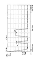
例えば、図1は、DACのアナログフィルタ要件を示しており、それは基本アナログ出力周波数はf0=10MHzで、これは10MHzのデジタル入力周波数に対応し、変換レートは1秒あたり30メガワード(Mwps)、即ち30メガサンプル(Msps)で、これはトップグラフ(top graph)用の30MHzの変換レートに等価であり、60Mwps即ち60Mspsの変換レートはボトムグラフ(bottom graph)用の60MHzの変換周波数に等価である。DACは、10MHzのデジタル信号を10MHzの基本アナログ信号イメージ12aに変換する。30MHzの変換レートでは、DACは基本アナログ信号12aの20MHzでミラーイメージ14aを出力する。
【0007】
信号バンド幅とこの信号バンド幅のミラーイメージは、変換レートに対応する周波数インターバルで周期的に繰り返されるために、アナログ信号のレプリカイメージ12bは40MHzで生成され、ミラーイメージ14bは50MHzで生成され、レプリカイメージ12cは70MHz、ミラーイメージ14cは80MHzで生成される。30MHzの変換レートのDACにおいては、現在の設計慣行ではアナログローパスフィルタ(LPF)を用いてDACの出力からイメージ12b−cと14a−cを取り除き、基本10MHzアナログ信号イメージを適宜のRF周波数に変換して送信する。
【0008】
60MHz(即ち、60Msps,60wps)の変換レートでは、DACは基本の10MHzアナログ信号イメージ16aと50MHzでミラーイメージ18aを出力する。信号バンド幅とこの信号バンド幅のミラーイメージは、変換レートに対応する周波数インターバルで周期的に繰り返されるために、アナログ信号のレプリカイメージ16bは、70MHzで生成され、ミラーイメージ18bは110MHzで生成される。上記したように、現在の設計慣行は、アナログローパスフィルタ(low pass filter,LPF)を用いてDACの出力からイメージ16b,18a,18bとを除去し、基本10MHzアナログ信号イメージを適宜のRF周波数に上方変換して送信している。
【0009】
【発明が解決しようとする課題】
技術が進歩するにつれてDACの変換レートが増加している。しかし、現在の送信機アーキテクチャは、DACにより得られる基本的なコスト削減およびフレキシビリティを利用していない。
【0010】
【課題を解決するための手段】
本発明は、デジタルからアナログへの変換器(DAC)を用いて、デジタル信号をアナログ形式に変換し、DACにより生成されたアナログ信号イメージを用いて送信周波数でアナログ信号を与え、あるいは/それと同時に投影(projected)されたアナログ信号イメージを用いて送信用のアナログ信号を生成する。DACの出力点にあるローパスフィルタでもってアナログ信号イメージを除去する代わりに、あるいはアナログ信号イメージおよび周波数変換用のアナログミキサを用いる代わりに、デジタル送信機はDACからのアナログ信号イメージを用いて所望の周波数でもってアナログ信号を生成する。
【0011】
DAC用の変換レートあるいはデジタル信号周波数を設定あるいは調整することにより、DACから生成されたアナログ信号イメージを所望の周波数バンドに配置することができる。例えばデジタル送信機は、DAC用の変換レートの2分の1として定義された変換バンド幅のオーバラップしない部分内にデジタル信号を配置することができる。デジタル信号がアナログ形式に変換されると、DACは、変換レートの2分の1の整数倍で周期的に繰り返されるアナログ信号イメージを生成し、かくしてアナログ信号イメージは、増幅用および送信用に適した適宜の周波数バンドで生成される。
【0012】
【発明の実施の形態】
次にデジタルからアナログへの変換器(DAC)を有するデジタル送信機システムが、デジタル信号をアナログ形態に変換して、その結果得られたアナログ信号イメージを用いて送信用のアナログ信号を生成する状態を示す。図2aは、少なくとも1個のデジタル信号を受領するDAC22を有するデジタル送信機20を示す。DAC22は、変換レートfcでデジタル信号スペクトラムを変換する。DACの変換レートfcは、0Hzから変換レートの2分の1までの変換バンド幅がデジタル信号のバンド幅を包含するよう選択される。変換レートが上がるにつれて、変換バンド幅が広がる。デジタル信号バンド幅が変換レートの2分の1以上の場合には、投影イメージの間に好ましくないオーバラップが発生する。
【0013】
図2bに示すように、DACはデジタル信号(F1−FN)を変換レートの2分の1に等しい変換バンド幅内の周波数F1からFNまでのデジタル信号を包含する変換レートfcを用いて変換する。デジタルスペクトラムを変換レートfcでアナログ形式に変換するに際し、変換バンド幅、即ち基本アナログイメージ24は変換周波数fcの2分の1の整数倍でもって周期的に回転し、即ちフォールド(fold)して、アナログ信号(F1−FN)を含む基本アナログイメージ24のミラー化された第1投影アナログイメージ26aとレプリカの第2投影アナログイメージ26bとミラー化された第3投影アナログイメージ26cを生成する。
【0014】
アナログイメージは、変換レートでもってデジタルスペクトラムをアナログ形式に変換することにより、0Hzから変換レートの2分の1までに生成された基本アナログイメージとも、この基本アナログイメージの投影されたレプリカとも、即ちミラー化されたアナログイメージとも称する。アナログ信号イメージは、基本アナログ信号イメージおよびデジタル信号スペクトラム内の特定のデジタル信号をアナログ形式に変換することにより得られた基本アナログ信号イメージの対応する投影されたアナログ信号イメージと称する。
【0015】
変換レートまたはデジタル信号周波数またはその両方を設定することにより、変換されたデジタル信号は、デジタル信号がアナログ形式に変換されアナログ信号イメージが所望の周波数にあるような周波数に位置する。基本アナログ信号イメージが、所望の伝送周波数にあるときには、基本アナログ信号イメージは直接増幅され、アナログ領域で周波数変換を行うことなく所望の伝送周波数で送信することができる。しかし、基本アナログ信号イメージが所望の伝送周波数にないときには、デジタル送信機は、基本アナログ信号イメージから投影された後続のアナログ信号イメージを用いて伝送用に所望のアナログ信号を生成する。
【0016】
かくして、アナログ信号イメージを基本アナログ信号イメージからフィルタ処理する代わりに、所望の伝送周波数に入る投影されたアナログ信号イメージを直接増幅し送信することができる。この投影されたアナログ信号イメージもまた所望の中間周波数(intermediate frequency,IF)上に入り、この周波数は増幅用および伝送用の中間周波数あるいは最終的に伝送周波数に周波数変換することができる。所望の中間周波数の投影されたアナログ信号イメージを用いることにより周波数変換段の数を減らすことができる。
【0017】
投影されたアナログ信号イメージは、基本アナログ信号イメージのレプリカあるいはミラーイメージと称する。かくして、デジタル送信機はアナログイメージをフィルタ除去する必要がなく、またアナログ信号を適宜の伝送バンドに配置するためにアナログ領域内の周波数変換にのみ依存することもない。
【0018】
デジタル送信機は、変換レートにより確立された変換バンド幅の柔軟性および効率的な利用を提供することができる。例えば、アナログ形式に変換されるデジタル信号が不連続の周波数バンドで送信される場合には、変換バンド幅は、十分に高い変換が利用可能な場合には、不連続のバンドを包含する。そうでない場合あるいは望ましい場合には、デジタル送信機は変換バンド幅内のデジタル信号を、送信周波数における対応するアナログ信号間の相対的位置とは独立した位置に配置することができる。
【0019】
例えばデジタル信号は、伝送周波数の対応するアナログ信号よりも変換バンド幅内で互いに近く配置することができる。デジタル送信機がデジタル信号をアナログ形式に変換した後、異なるゾーン(または変換レートの2分の1の異なる整数倍)のアナログ信号イメージを用いて不連続の伝送バンド内にアナログ信号を生成することができる。
【0020】
別法として、デジタル送信機は複数の無線通信周波数(PCSまたはセルラ)または複数の無線通信プロトコール(CDMA,GSM,北米TDMAその他)を用いて通信することができる。かくして、デジタル送信機(基地局または無線機器)により使用される無縁通信周波数または無線通信プロトコールによって、アナログ信号イメージが所望の伝送周波数上にあるように使用される変換レートが設定されデジタル信号の位置が調整される。
【0021】
さらにまた、無線機器が無線通信システムにアクセスを試みようとしているときに、無線機器はそのシステムで使用される無線通信周波数またはプロトコールの種類の情報には依存せず、あるいはシステムは複数の不連続周波数バンドまたはプロトコールを用いることをができる。
【0022】
無線通信システムにアクセスし通信するために無線機器は、デジタル信号周波数または変換レートを設定して、異なる周波数バンドあるいはプロトコールを用いて同時にアナログ信号を送信する。無線機器は、アナログ信号の送信用には一時に1個の周波数バンド/プロトコールの組合せを用い、例えば少なくとも1個の異なる周波数バンドに対応する各アナログ信号伝送用に変換レートまたはデジタル信号周波数を変えることにより送信する。
【0023】
所望のタイプのアナログ信号伝送用のデジタル信号周波数または変換レートは、単一の周波数バンド/プロトコール構築用に予め設定され、複数の周波数/プロトコール構築用には、予め設定され記憶されあるいは実施例によっては、無線機器または無線通信システムから受領したまたは無線機器または基地局内で決定されあるいは計算される。
【0024】
図2aの実施例においては、信号分配ネットワーク、即ちカップリングネットワーク30、例えばパワーディバイダーあるいはNプレクサは、DAC22からアナログ信号スペクトラム全体を受領し、このアナログ信号あるいはその一部を組み合わせたり分離したりそしてアナログ信号を送信または増幅またはチャネルブランチ、即ちパス31a−xに与える。例えば、パス31a−xは対応するRF周波数バンドでアナログ信号を搬送し、異なるアンテナまたはアンテナの組み上に送信すべきアナログ信号を搬送し、異なるあるいは連続する周波数バンドのアナログ信号のコピーを有する。
【0025】
実施例によっては、カップリングネットワーク30はDAC22から各フィルタ32a−xへの直接接続を含み、各フィルタ32a−xは対応するアンテナ36a−xに接続される。送信機20が、1本の伝送ブランチ31のみを有する場合にはカップリングネットワーク30はDAC22からフィルタ32、増幅器34を介してアンテナ36への接続を有する。パス31a−x、フィルタ32a−x、増幅器34a−xの数は、複数で互いに等しい場合もあれば異なる場合もある。
【0026】
いずれの場合においてもカップリングネットワーク30は、信号f1からfNをパス31a−xに与えて増幅と送信を行う。図2aの実施例においては、カップリングネットワーク30のバンドパスフィルタ32a−32xにより所望の周波数f1からfNのアナログ信号は、対応するパス31a−x上を通過するが、他の信号周波数は減衰する。所望のアナログ信号f1からfNは、増幅器34a−xにより増幅されアンテナ36a−xにより送信される。
【0027】
図2bに示すように、アナログ信号用の所望の周波数f1−fNは、アナログ信号スペクトラムの異なる場所にある。例えば、増幅と送信用のアナログ信号f1は、変換バンド幅内のアナログ信号バンド幅(F1−FN)の一部の上、あるいは0Hzから1/2fcの間の基本アナログイメージの一部の中にある。アナログ信号fNは、変換周波数fcのn−1倍のレプリカイメージ26bの一部の中にある。アナログ信号が所望の周波数(f1−fN)で分離された後、増幅器34a−xが所望の周波数でアナログ信号を増幅し、アンテナ36a−xを介して送信される。
【0028】
図2aの実施例においては、送信機20は信号処理装置(SPU)42a−iを有し、このSPU42a−iがm個のデジタル信号、即ちストリームD1からDm、例えばベースバンドデジタル情報信号を受領する。SPUが単一のデジタル信号と複数のデジタル信号、この複数のデジタル信号を含む合成デジタル信号のいずれかあるいはそれらのいくつかを受領する。この実施例においては、SPU42a−iは、少なくとも1個のデジタル信号を受領する。SPU42a−iが複数のデジタル信号を含むデジタル信号(例えば8−10kbpsの10個の音声の呼び用のデジタルベースバンド情報信号)を受領すると、これらのデジタル信号が全て一緒にされる。
【0029】
各SPU42a−iは、デジタル信号を符号化しこのデジタル信号に対しエラー修正情報を付加し、ビットインターリーブを実行し、デジタル信号上で同位相(I)と直交相(Q)の変調を実行し、デジタル周波数変換を実行し、アップ(またはダウン)でデジタル中間周波数(IF)信号を生成する。変換バンド幅内のデジタル信号の一部が調整を必要とする場合には、デジタル周波数コンバータは、例えば数値制御発振器(numerically controlled oscillator,NCO)と、周波数スペクトラムを配置するデジタルミキサとを用いてベースバンドのデジタル信号またはデジタルIF信号を同調して、デジタル信号をDAC用の変換バンド幅内に適切に配置し、その結果得られたアナログ信号がDAC22の出力点で所望の周波数帯域に入るようにする。
【0030】
図2aの実施例においては、SPU42a−iは少なくとも1個のデジタル信号の処理から得られたデジタルI/Q変調信号(デジタル中間周波数(IF))を対応するバス44a−i上に生成する。バス44a−iはコンバイナ(結合器)46に与えられ、このコンバイナ(結合器)46は、例えばバス加算器として機能するフィールドプログラマブルゲートアレイ(field programmable gate array,FPGA)である。コンバイナ(結合器)46は異なるバス44a−iからのデジタル信号のデータエッジとクロックとを整合させ、バス44a−i上のデジタル信号をバス48上に加算する。
【0031】
一実施例においては、各バス44a−iはデジタルデータの68(Mwps)を取り扱う18ビットバスである。ここで、ワードとはバスの幅で、バス48は、68Mwpsを処理できる14ビットバスである。5個のSPU42a−iがある場合には、各SPU42a−iは最大10個のボイスコールを処理でき、バス48は最大50個のボイスコール用のデジタル信号を搬送することができる。このバス48は、混成(合成)デジタル信号をDAC22に与え、DAC22は68MHzの変換レートで動作する14ビットDACである。この実施例においては、DACは14ビットデバイスであり、加算されるべき各バス44a−iは、18ビット(プラス符号ビット)であるために、FPGAである結合器46は来入するバス44a−iの得られた和上の切り捨てを実行する。この切り捨ては、ゲイン調整とも通常称する。
【0032】
前述したように、DAC22用の変換レートは、デジタル情報信号の全バンド幅が変換レート、即ち変換周波数の少なくとも2分の1である変換バンド幅により包含されるよう選択される。さらに、別のデジタル信号は、変換バンド幅のオーバラップしない部分を専有し、延ばして(fold out)各対応するデジタル信号用に所望の周波数バンドでアナログ信号イメージを生成する。この所望の周波数バンドのアナログ信号イメージを用いて、アナログ信号を生成してRFで送信する。
【0033】
図3は、混成(合成)デジタル信号の0Hzから50MHzの周波数スペクトラム解析を示す。このグラフは、合成デジタル信号上にフーリエ変換を実行することにより得られた。合成デジタル信号は、デジタル信号とも称するが、中心周波数が10MHzで2MHzのバンド幅で振幅が−10dBmの(CDMA)デジタル信号50と、中心周波数が20MHzでバンド幅が7MHzで振幅が−4dBmの(FM)デジタル信号52とを有する。合成デジタル信号がDACに与えられ、アナログ形式に変換される。
【0034】
図4は、図3の合成デジタル信号から得られたDACの出力の0から50MHzの周波数スペクトラムの解析結果で、DACが50MHzの変換レート、即ち周波数で動作する。0Hzから1/2fc(これは変換バンド幅でゾーン0と称称する)では基本アナログ信号イメージ60と62がデジタル信号50,52のデジタルからアナログへの変換結果として表れる(図3)。
【0035】
かくして、基本アナログ信号イメージ60は図3のCDMAデジタル信号50に対応し、基本アナログ信号イメージ62は図3のFMデジタル信号52に対応する。同図に示すように、アナログ信号イメージ60は中心周波数が10MHzの場所にあり、バンド幅は2MHzで振幅は−26dBmである。アナログ信号イメージ62は中心周波数が20MHzの場所にあり、バンド幅は7MHzで振幅は−22dBmである。
【0036】
上記したように、変換バンド幅内のスペクトラムは、変換レートの1/2のインターバルで広がり(folds up)、基本イメージの投影されたレプリカイメージとミラーアナログイメージとを生成する。図4においては、変換バンド幅あるいはゾーン0は、25MHz(変換レートの2分の1)でホールドし、25MHzから50MHz(ゾーン1と称する)までの基本アナログイメージ24のミラー化アナログイメージ26aを生成する。ゾーン1においては、アナログ信号イメージ64aは、FMアナログ信号イメージ62のミラーイメージである。
【0037】
アナログ信号イメージ64aは中心周波数が30MHzで、バンド幅が−7MHzで、振幅は−25dBmである。アナログ信号イメージ66aは、CDMAアナログ信号イメージ60のミラーイメージである。アナログ信号イメージ66aは、中心周波数が40MHzで、バンド幅が2MHzで、振幅が−38dBmである。図の間の振幅の差は、図の間のスペクトラムアナライザに変化(例えば、解像度のバンド幅、ビデオバンド幅(video bandwidth,VBW)を付けたことにより得られたもの、スイープレート、スパンとスタート/ストップ)である。この変動を設定することは、スペクトラムアナライザの解像度と精度に影響を及ぼす。
【0038】
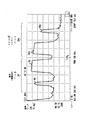
図5は、スペクトラムアナライザの感度を高い状態に設定した0から100MHzの周波数スペクトラムのグラフである。上記したように、基本アナログ信号イメージを含む変換バンド幅24即ちゾーン0(基本アナログイメージ)のレプリカとミラーの投影アナログイメージが変換周波数の周波数インターバルで繰り返して表れる。図5においては、ゾーン1は、基本アナログイメージあるいはゾーン0のミラー化された第1投影アナログイメージ26aであり、ゾーン2は基本アナログイメージあるいはゾーン0のレプリカの第2の投影アナログイメージ26bであり、ゾーン3は基本アナログイメージあるいはゾーン0のミラー化された第3投影アナログイメージ26cである。
【0039】
かくして、ゾーン2のアナログ信号イメージ66bはCDMAアナログ信号イメージ60のレプリカであり、ゾーン2のアナログ信号イメージ64bは、FMアナログ信号イメージ62のレプリカである。CDMAアナログ信号イメージ66bは、中心周波数が60MHzでバンド幅が同じで振幅が15dB以下である。FMアナログ信号イメージ64bは中心周波数が70MHzで、バンド幅は同じで、振幅は12dB以下である。
【0040】
ゾーン3においては、ゾーン3のアナログ信号イメージ66cはCDMAアナログ信号イメージ60のミラーイメージであり、ゾーン3のアナログ信号イメージ64cはFMアナログ信号イメージ62のミラーイメージである。FMアナログ信号イメージ64cは中心周波数が80MHzでバンド幅が同一で、振幅はゾーン2のFMアナログ信号イメージ64bより約1dB小さい。CDMAアナログ信号イメージ66cは中心周波数が90MHzでバンド幅が同一で振幅がゾーン2のCDMAアナログ信号イメージ66bよりも4dB小さい。
【0041】
図6は、投影アナログイメージ26r−uを含む450MHzから550MHzの周波数スペクトラムを表すグラフである。図6において、投影アナログイメージ26rは基本アナログイメージあるいはゾーン0の18番目の投影イメージ、即ちゾーン18である。アナログイメージ26r、即ちゾーン18は基本アナログイメージ、即ちゾーン0のレプリカである。CDMAアナログ信号イメージ66rはCDMAアナログ信号イメージ60(図5)のレプリカであり、FMアナログ信号イメージ64rはFMアナログ信号イメージ62のレプリカ(図5)である。CDMAアナログ信号イメージ66rは中心周波数が460MHzで、振幅はCDMAアナログ信号イメージ60の振幅より約39dB小さい。FMアナログ信号イメージ64rは中心周波数が470MHzで、振幅はFMアナログ信号イメージ62(図5)の振幅より約29dB小さい。
【0042】
投影アナログイメージ26sは基本アナログイメージ、即ちゾーン0の19番目の投影されたアナログイメージ、即ちゾーン19である。アナログイメージ26s、即ちゾーン19は基本アナログイメージ、即ちゾーン0のミラーイメージである。CDMAアナログ信号イメージ66sはCDMAアナログ信号イメージ60のミラーイメージであり、FMアナログ信号イメージ64sはFMアナログ信号イメージ62のミラーイメージである。
【0043】
CDMAアナログ信号イメージ66sは中心周波数が490MHzで、振幅はCDMAアナログ信号イメージ66rの振幅より若干小さい。FMアナログ信号イメージ64sは中心周波数が480MHzで、振幅はFMアナログ信号イメージ64rの振幅より約1dB小さい。
【0044】
投影アナログイメージ26tは基本アナログイメージ、即ちゾーン0の20番目のイメージ、即ちゾーン20である。投影アナログイメージ26t、即ちゾーン20は、基本アナログイメージ、即ちゾーン0のレプリカである。CDMAアナログ信号イメージ66tは、CDMAアナログ信号イメージ60のレプリカであり、FMアナログ信号イメージ64tは、FMアナログ信号62のレプリカである。
【0045】
CDMAアナログ信号イメージ66tは、中心周波数が510MHzで、振幅は、CDMAアナログ信号イメージ66sのそれと同じである。FMアナログ信号イメージ64tは中心周波数が520MHzで、振幅はFMアナログ信号イメージ64sのそれよりも3dB小さい。
【0046】
最後に、投影アナログイメージ26uは基本アナログイメージ、即ちゾーン0の21番目の投影アナログイメージ、即ちゾーン21である。投影アナログイメージ26u、即ちゾーン21は、基本アナログイメージ、即ちゾーン0のミラーイメージである。CDMAアナログ信号イメージ66uは、CDMAアナログ信号イメージ60のミラーイメージであり、FMアナログ信号イメージ64uは、FMアナログ信号イメージ62のミラーイメージである。
【0047】
CDMAアナログ信信号対ノイズ比(SNR)を維持しながらノイズフロアーをできるだけ低く維持することができる。
【0048】
さらにまた、デジタル領域またはアナログ領域で振幅等価フィルタリングを実行することにより、アナログ信号イメージ上にDACにより導入された振幅の減少または振幅歪みを補償することができる。例えば、フィルタリングは、アナログ信号イメージに対する所望の周波数でアナログ信号イメージ上にDACにより導入されたsinx/xあるいは他の影響を補償するためにsinx/x関数あるいは他の関数の逆関数を実行する。
【0049】
図7は、1MHzから700MHzの周波数スペクトラムの700MHzに亘るDAC出力のグラフである。上記したように、変換レートあるいは周波数の各インターバル70a−nはゾーン0の基本アナログイメージのレプリカアナログイメージ(インターバル70aの基本アナログイメージそのもの)とミラーアナログイメージとを含む。
【0050】
アナログイメージは、このような広い周波数スパンに亘ってスペクトルアナライザーの解像度に限界があるため、上記したようには表れない。図7は、アナログ信号イメージの振幅が、周波数が増加するにつれていかに減少するかを示している。この実施例においては、アナログ信号イメージは、周波数インターバル70aから周波数インターバル70nにかけて約30dB減少し、これはアナログイメージの振幅がsinx/xあるいはsinc関数の悪化による。
【0051】
かくして、本発明によるデジタル送信機は周波数変換段を減少あるいは除去し、所望の周波数のアナログ信号イメージを用いることによりDACの出力点のローパスフィルタを取り除くとができ、これによりベースバンドのアナログ信号と中間周波数(IF)と無線周波数(RF)を生成する。さらにまた、DACに用いられる変換レートによっては、異なるデジタル信号が変換バンド幅のオーバーラップしない部分に配置することができ、かつ異なるアナログ信号イメージあるいはその一部を異なるアナログベースバンドに配置することができ(IF)周波数信号または(RF)周波数信号あるいはその両方にアナログ信号送信用に用いることができる。
【0052】
例えば上記の例においては、第1ゾーン(ゾーン1)からのFMアナログ信号イメージを用いてRFでFMアナログ信号を送信する。第2ゾーンからのCDMAアナログ信号イメージを用いてRFを介して無線でCDMAアナログ信号イメージを送信することができる。このためデジタル送信機20(図2)は、単一のDACで利用可能な変換バンド幅を用いて異なるRF周波数バンドでRFアナログ信号を生成することができる。
【0053】
実施例によっては、および本発明のデジタル送信機の柔軟性に起因して送信機は、様々な方法でDAC22の潜在的な変換バンド幅を用いることができる(図2a)。例えば、Bバンドのサービスプロバイダに対しては、セルラ基地局の送信BとB′のバンド幅(880−890と891.5−894MHz)を介して送信される通信用のデジタル信号はDAC22の変換バンド幅の全部で14MHzの部分に配置することができ(RFにおけるBとB′バンドの間の関係がデジタル領域におけるBとB′のバンドでも維持される場合)、その結果得られたゾーン0のセルラアナログ信号バンド幅は880−894MHzのセルラ基地局の送信バンド幅に広げられる(folds out)。
【0054】
PCS基地局送信バンド(1945−1950MHz)のDブロックを介して通信されるデジタル信号は、変換バンド幅の5MHz部分内に配置することができ、これはセルラバンドとオーバラップすることがなく、その結果得られたゾーン0のPCSアナログ信号バンド幅は、(1945−1950MHz)のPCS基地局送信バンドのDブロックまで広げられる。さらにまたこの実施例においては、FM無線周波数バンド(88から108MHz)で送信されるべきデジタル信号情報は、DAC22の変換バンド幅の20MHzの部分内に配置することができ、その結果得られたFM無線アナログ信号バンド幅は88−108MHzのFM無線バンドまで広げられる。
【0055】
この実施例においては、変換バンド幅の異なる部分のRFアナログ信号の全バンド幅は、セルラバンド(14MHz)と、PCSDブロック(5MHz)と、FM無線バンド(20MHz)が追加された後では39MHzである。かくして、DAC22の変換レートを用いて、変換バンド幅はRFアナログ信号の39MHzバンド幅を処理するのに十分なものとなる。例えば、39MHzのバンド幅の最小値においては、変換レートは少なくとも78MHzでなければならない。
【0056】
DAC22の変換レートは、異なる周波数バンドが所望の周波数バンド内に再形成されるように選択される。かくして適宜の変換レートの選択は、変換バンド幅からアナログイメージの所望の周波数バンドへ異なる周波数バンドを相対的に配置することにより行われる。実際には、変換レートは異なる周波数バンドの信号間にガードバンドを提供するよう選択される。
【0057】
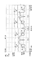
この実施例においては、図8は300MHzの対応する変換バンド幅でDACが600MHzの変換レートを有する結果得られたDACの出力を示す。変換バンド幅内でFMデジタル信号バンド幅は88から108MHzに配置され、PCSのDブロックのデジタルバンド幅は145−150MHzに配置され、セルラBバンドデジタルバンド幅は208−294MHzに配置される。DACは、デジタルスペクトラムをアナログ形式に変換し、その結果基本イメージ80は変換バンド幅内に入り、基本アナログ信号イメージ82は88−108MHzで、基本アナログ信号イメージ84は145−150MHz(PCSDブロック)で、基本アナログ信号イメージ86は280−294MHzである。
【0058】
変換バンド幅は変換レートの1/2のインターバルで自分自身の周囲で広がる(folds about itself)。次に基本FMアナログ信号イメージ82は適宜の伝送周波数にある。かくしてデジタル送信機は、88−108MHzでエアー(無線)を介して伝送するために、基本FMアナログ信号イメージ82を用いることができる。奇数番号のゾーンである88a,c,e,g内では、ゾーン0のミラーイメージ80が形成され、一方偶数番号のゾーンである88b,d,fではゾーン0のレプリカイメージが形成される。かくして、ゾーン88a−gではDACの出力はFMアナログ信号イメージ90a−gを含み、これはこの実施例では用いられない。
【0059】
信号バンド幅のミラーリングと脱ミラーリングは、例えばデジタル領域に変換する間、あるいはその前に同位相(I)成分と、直交相(Q)成分を交換することにより容易に実行され、その結果伝送用のミラー化されたアナログ信号イメージが所望のスペクトラム関係を有する。ミラー化されたアナログ信号イメージの所望のスペクトラム関係は、デジタル信号を処理することにより行われ、その結果得られた伝送用のミラー化(ミラー)アナログ信号イメージは所望のスペクトラム位置(例えば、脱ミラー化)を有する。別法として、受信機はミラー化アナログ信号イメージを受領し、所望のアナログ信号イメージを形成するためにスペクトラムの脱ミラー化(de-mirroring)あるいはフォールディング(拡張:folding)を実行する。
【0060】
基本FMアナログ信号イメージ82は88−108MHzの伝送周波数にあるために、デジタル送信機は増幅用と送信用に88−108MHzの基本FMアナログ信号イメージを用いることができる。セルラBバンドアナログ信号イメージ94bはセルラBバンド用の伝送周波数880−894MHzに入り、その結果セルラBバンドアナログ信号イメージ94bが増幅され、セルラBバンドに送信される。PCSDブロックアナログ信号イメージ92fはPCSDブロック用の伝送周波数1945−1950MHzにあり、PCSDブロック、アナログ信号イメージ92fは増幅されPCSDブロックに送信される。
【0061】
図2aの実施例と図8の実施例を参照すると、DAC22の出力をカップリングネットワーク30が受領する。カップリングネットワーク30内でバンドパスフィルタ32aは88−108MHzのFMブロードキャストバンドに対応する。かくして、フィルタ32aにより88MHz−108MHzの間の周波数はパス31a上を通過し、その間に他の周波数は減衰する。パス31a上の基本FMアナログ信号イメージ82は、増幅器34aにより増幅され、アンテナ36aから送信される。
【0062】
バンドパスフィルタ32bは、セルラBバンド周波数あるいはその一部に対応し、880−894MHzの間の周波数はパス31b上を通過し、その間に他の周波数は減衰する。パス31b上のセルラBバンドアナログ信号イメージ94bは増幅器34bにより増幅され、アンテナ36bから送信される。最後に、バンドパスフィルタ32xはPCSDブロックの周波数あるいはその一部に対応し、1945−1950MHzの間の周波数はパス31y上を通過し、その間に他の周波数は減衰する。パス31y上のPCSDブロックアナログ信号イメージ92fは増幅器34yにより増幅され、アンテナ36zから送信される。
【0063】
かくして、この実施例においては、本発明による送信機はパス31a−xのいずれかの上に周波数変換段(ミキサ/LOの組合せ)を必要としない。ミキサ/LOを具備しない送信機は、コストを低減するだけでなくいくつかの利点がある。例えば、周波数変換段に固定したローカルオシレータ(local oscillater,LO)がない場合には、電子パワーの消費を減らすことができかつコストとサイズも減らすことができる。
【0064】
IFにおけるフィルタ要件を減らすあるいは削除することができ、同時にLO放射の除去のフィルタ要件も減らすことができる。ミキサが必要とされないために、ミキサからの偽信号およびミキサにより生成された変調間の歪みも除去することができ、これにより偽信号のないダイナミックレンジを改善することができ、要件を緩和することができる。さらにまた、ミキサにより導入される損失も除くことができ、これにより必要とされるチャネルゲインを減らし、ゲインの線形性を改善できる。
【0065】
DAC22に対する変換レートを適宜選択/設定することにより本発明の送信機は、DAC22により提供される変換バンド幅の利用率を向上させ大きな周波数差により分離された様々な異なる周波数バンドでRFアナログ信号を送信することができる。上記の例においては、FM無線スペクトラム全体と、セルラスペクトラムのBバンドと、PCSスペクトラムのDバンドを300MHzの変換バンド幅内のデジタル領域に配置することができ、それを600MHzの変換レートを有する単一のDACを用いてアナログ形式に変換することができる。
【0066】
変換バンド幅内のデジタル信号をアナログ信号に変換するに際し、DACは変換バンド幅内の変換されたデジタル信号の基本アナログイメージと、この基本アナログイメージのレプリカとミラーイメージとを生成し、これを用いて適宜の伝送周波数でアナログ信号を生成する。他の実施例においては、別の変換レートを用いて変換バンド幅を増加したり、減少したりすることができ、これにより余分のバンド幅あるいは異なる周波数バンドの信号間にガードバンドを提供することができる。
【0067】
したがって、本発明の送信機は、異なる多重アクセス技術あるいは同一の多重アクセス技術あるいはそれを使わずに、同一あるいは異なる変調技術または単一のDACコンバータ内で異なるあるいは連続する周波数バンドをRFバンドまたは送信用周波数バンドへの周波数変換を行うことなく、システムからの信号を送信することができる。アナログ信号は、ワイドバンドまたはブロードバンドまたはナローバンドとして特徴づけることができる。別の実施例は、アナログ信号イメージの周波数変換を有する。
【0068】
かくして、アナログ信号イメージは周波数変換を必要とするような中間周波数にあることがある。例えば、アナログ信号ミラーあるいはレプリカイメージは、無線周波数あるいは送信用周波数に周波数変換され、周波数変換段を減らしたり削減したりあるいは無線周波数または送信周波数でのアナログ信号イメージの位置を微調整することができる。
【0069】
上記の実施例に加えて、本発明の別の周波数アーキテクチャも可能であり、上記した周波数アーキテクチャの構成要素を追加したり省いたりあるいはそれらを修正することも可能である。例えば、AMブロードキャスト無線周波数バンド(550−1600kHz)を合成デジタル信号に付加することができ、DAC22がAM無線周波数バンド内でデジタル信号を変換することもできる。AM無線周波数バンドは、変換バンド幅のkHzの範囲に配置することが可能である。
【0070】
かくして本発明の送信機は、変換プロセスからのアナログ信号イメージを用いて様々なソース(例えば、セルラPCSネットワーク、AM/FM放送無線局、衛星システム、様々な物理的媒体に基づいた他のシステム)からの信号を同時に送信することができる。送信機のアーキテクチャおよびそれぞれの動作パラメータおよび特性を形成する様々な構成要素は、適切な動作を提供するために適宜マッチングされる。
【0071】
例えば、送信システムの一実施例を用いて異なるプロトコールとRF周波数を用いたシステム(例えば、北米TDMAシステム、GSM(Global System For Mobile Communication)システム、CDMAシステム、FDMAシステム、FM無線/AM無線システム)に従って信号を送信することができる。
【0072】
さらにまた本発明の送信機の一実施例は、不連続の周波数バンド内でアナログ信号を送信するために複数の個別のアナログ信号イメージを用いる例を用いて記載した。本発明によるデジタル送信機は、変換レートまたはデジタル信号周波数、例えばそれらは加入時にダイナミックかつ周期的に設定可能であり、製造時あるいは現場で制御可能であり、特定の周波数バンド内のアナログ信号の伝送用にアナログ信号を生成し、あるいはセルラBバンドにおいて例えばCDMAの特定の多重アクセス技術を用いて実行可能である。
【0073】
かくして、同一のハードウェアを異なる周波数のアナログ信号を送信するためあるいは異なる多重アクセス技術あるいはプロトコールを用いて送信するためのデジタル送信機用に用いることができる。
【0074】
好ましいプロトコールあるいは多重アクセス技術は、登録されたあるいはダウンロードして取得したソフトウェアまたは送信機を再構成することにより、例えばプログラマブル論理デバイスとを用いて提供することができる。
【0075】
上記の実施例において、伝送用の周波数バンドは基地局の送信用周波数に関連づけられる。しかし、本発明の送信機のアーキテクチャは無線ユニット、例えば移動機は異なる周波数バンドで情報を送信する。例えば、同一あるいは異なる多重アクセスシステムを用いてPCS周波数またはセルラ周波数上で送信できこれにより複数の無線通信システムへのアクセスを与える。
【0076】
1個あるいは複数の無線通信システムへのアクセスが得られた後、デジタル送信機は、対応する周波数バンドで1つあるいは複数の無線通信システムで送信を継続することができる。かくして、無線機器のカバレッジ領域あるいは機能によって無線機器あるいは無線基地局は、製造時あるいは動作時あるいは設定値にダイナミックにあるいは周期的にデジタル信号の変換レートまたは周波数を調整して所望のバンドで伝送できるようアナログ信号イメージを配置できる。
【0077】
これにより、送信機アーキテクチャのフレキシビリティが増し、動作周波数を変化させたり別の動作周波数を与えることができる。その理由は、製造時あるいは設定後、通常固定される送信パス上でアナログ周波数の変換を必要としないからである。
【0078】
さらにまた、送信システムは個別の構成要素の特定の組合せでもって記載したが、送信システムおよびその一部は特定アプリケーション用の集積回路、ソフトウェア駆動の処理回路、ファームウェア、プログラマブル論理回路、ハードウェアあるいは他の個々の構成要素の別の組合せを用いて実現することもできる。
【0079】
本発明は特定の回路でもって示したが、本発明のアーキテクチャは実施例に開示した回路と類似の機能を実行する異なる構成要素を用いることも可能である。上記の説明は本発明の単なる一実施例であり、様々な変形修正が可能である。しかし、これらの変形修正も本発明の範囲に入るものである。
【図面の簡単な説明】
【図1】DACの出力からのアナログ信号イメージをいかにフィルタ除去するかの従来の一般的なグラフを表す図
【図2】A 本発明による送信機の一実施例のブロック図
B Aの送信機用のDACの出力のグラフ
【図3】本発明により送信されアナログ形式に変換されたデジタル信号の周波数領域のグラフ
【図4】図3のデジタル信号を50MHzの変換周波数を用いてアナログ形式に変換した結果により得られたDACの出力点における0から50MHzのスパンのアナログ信号イメージを表す図
【図5】図3のデジタル信号を50MHzの変換周波数を用いてアナログ形式に変換した結果により得られたDACの出力点における0から100MHzのスパンのアナログ信号イメージを表す図
【図6】図3のデジタル信号を50MHzの変換周波数を用いてアナログ形式に変換した結果により得られたDACの出力点における450から550MHzのスパンのアナログ信号イメージを表す図
【図7】図3のデジタル信号を50MHzの変換周波数を用いてアナログ形式に変換した結果により得られたDACの出力点における0から700MHzのスパンのアナログ信号イメージを表す図
【図8】PCSデジタル信号、セルラデジタル信号、FMデジタル信号を600MHzの変換周波数を用いてアナログ形式に変換した結果により得られたDACの出力点における0から2400MHzのスパンのアナログ信号イメージを表す図
【符号の説明】
12a 基本アナログ信号イメージ
12b,12c レプリカイメージ
14a,14b ミラーイメージ
20 デジタル送信機
22 DA変換器(DAC)
24 基本アナログイメージ
26 投影アナログイメージ
26a ミラー化された第1投影アナログイメージ
26b レプリカの第2投影アナログイメージ
26c ミラー化された第3投影アナログイメージ
30 カップリングネットワーク
31 パス
32 バンドパスフィルタ
34 増幅器
36 アンテナ
42 信号処理装置(SPU)
44,48 バス
46 結合器
50 CDMAデジタル信号
52 FMデジタル信号
60,66b,c,r,s,t,u CDMAアナログ信号イメージ
62,64b,c,s,t,u FMアナログ信号イメージ
64a,66a アナログ信号イメージ
80 ミラーイメージ
82 基本FMアナログ信号イメージ
84,86 基本アナログ信号イメージ
90 FMアナログ信号イメージ
94b セルラBバンドアナログ信号イメージ
92f PCSDブロックアナログ信号イメージ[0001]
BACKGROUND OF THE INVENTION
The present invention relates to wireless communication technology, and more particularly to the architecture of a digital transmitter in a wireless communication system.
[0002]
[Prior art]
The service area of the wireless communication system is divided into a plurality of service areas called cells, and the wireless device communicates with a base station (BS) serving the cell via a wireless link. The base stations are connected to a terrestrial network, and are connected to a plurality of base stations distributed in a service area via, for example, a mobile switching center (MSC). In the wireless communication industry, service providers are provided with a plurality of non-consecutive or divided frequency bands that are used for transmission and reception of RF communication channels.
[0003]
For example, in the United States, base stations for "A" band (band) providers for cellular communications are in the bands of A (825-835 MHz), A '(845-846.5 MHz), A "(824-825 MHz). The frequency channel is received and transmitted on the frequency channel within the bandwidth of A (870-880 MHz), A ′ (890-891.5 MHz), A ″ (869-870 MHz). A base station for a B-band provider receives a channel in a frequency band of B (835-845 MHz) and B ′ (846.5-849 MHz), and B (880-890 MHz), B ′ (891.5-894 MHz). ) Is transmitting within the frequency band. Further, a base station for a personal communication system (PCS) receives a frequency channel from a wireless device on a block of a PCS band (1850 MHz-1910 MHz) and a frequency on a block of the PCS band (1930-1990 MHz). The channel is being transmitted.
[0004]
In a typical transmitter architecture, the baseband information signal is a digital signal provided to a signal processing unit (SPU). The SPU receives a baseband digital signal, and performs digital modulation on the digital signal in encoding, error detection processing, bit interleaving, in-phase (I) and quadrature (Q) modulation. Execute. The resulting digital (I / Q) modulated intermediate frequency (IF) signal is provided to a digital to analog converter (DAC). The DAC converts a digital IF signal into an analog IF signal, and the analog IF signal is converted into an analog radio frequency (RF) signal using an analog mixer and transmitted in an appropriate frequency band. A common transmitter that simultaneously processes and transmits signals within discontinuous frequency bands reduces the cost of system hardware.
[0005]
At present, the transmission system has an analog low-pass filter that removes the periodic image of the high-frequency analog IF signal generated by the DAC as a result of the digital to analog conversion process. When the digital IF spectrum is converted to the analog domain by the DAC at the conversion rate, the signal bandwidth periodically rotates, ie, is held at a multiple of one-half the conversion frequency. Thus, the replica image and the mirror image of the signal bandwidth are periodically repeated at a frequency interval corresponding to the DAC conversion rate.
[0006]
For example, FIG. 1 shows the analog filter requirements of a DAC, which has a fundamental analog output frequency of f 0 = 10 MHz, which corresponds to a digital input frequency of 10 MHz, with a conversion rate of 30 megawords per second (Mwps),
[0007]
Since the signal bandwidth and the mirror image of this signal bandwidth are periodically repeated at a frequency interval corresponding to the conversion rate, the analog signal replica image 12b is generated at 40 MHz, and the mirror image 14b is generated at 50 MHz. The
[0008]
At a conversion rate of 60 MHz (ie, 60 Msps, 60 wps), the DAC outputs a basic 10 MHz
[0009]
[Problems to be solved by the invention]
As technology advances, DAC conversion rates are increasing. However, current transmitter architectures do not take advantage of the basic cost savings and flexibility afforded by DACs.
[0010]
[Means for Solving the Problems]
The present invention uses a digital-to-analog converter (DAC) to convert a digital signal to analog form and uses the analog signal image generated by the DAC to provide an analog signal at the transmission frequency and / or simultaneously. An analog signal for transmission is generated using the projected analog signal image. Instead of removing the analog signal image with a low-pass filter at the DAC output point, or instead of using an analog mixer for analog signal image and frequency conversion, the digital transmitter uses the analog signal image from the DAC to Generate an analog signal with frequency.
[0011]
By setting or adjusting the DAC conversion rate or digital signal frequency, the analog signal image generated from the DAC can be arranged in a desired frequency band. For example, a digital transmitter can place digital signals within non-overlapping portions of the conversion bandwidth defined as one half of the conversion rate for the DAC. When a digital signal is converted to analog form, the DAC generates an analog signal image that repeats periodically at an integer multiple of one-half the conversion rate, thus the analog signal image is suitable for amplification and transmission. Generated in an appropriate frequency band.
[0012]
DETAILED DESCRIPTION OF THE INVENTION
Next, a digital transmitter system having a digital-to-analog converter (DAC) converts the digital signal to analog form and uses the resulting analog signal image to generate an analog signal for transmission Indicates. FIG. 2a shows a
[0013]
As shown in FIG. 2b, the DAC converts the digital signal (F1-FN) to a conversion rate f that includes digital signals from frequencies F1 to FN within a conversion bandwidth equal to one half of the conversion rate. c Use to convert. Digital spectrum conversion rate f c When converting to analog format, the conversion bandwidth, that is, the
[0014]
The analog image is generated by converting the digital spectrum into an analog format at a conversion rate, and thus a basic analog image generated from 0 Hz to half the conversion rate, and a projected replica of the basic analog image, that is, Also referred to as a mirrored analog image. An analog signal image is referred to as a corresponding projected analog signal image of the base analog signal image obtained by converting the base analog signal image and a particular digital signal in the digital signal spectrum to analog form.
[0015]
By setting the conversion rate and / or digital signal frequency, the converted digital signal is located at a frequency such that the digital signal is converted to analog form and the analog signal image is at the desired frequency. When the basic analog signal image is at the desired transmission frequency, the basic analog signal image is directly amplified and can be transmitted at the desired transmission frequency without frequency conversion in the analog domain. However, when the basic analog signal image is not at the desired transmission frequency, the digital transmitter uses the subsequent analog signal image projected from the basic analog signal image to generate the desired analog signal for transmission.
[0016]
Thus, instead of filtering the analog signal image from the base analog signal image, the projected analog signal image falling within the desired transmission frequency can be directly amplified and transmitted. The projected analog signal image also enters a desired intermediate frequency (IF), which can be frequency converted to an intermediate frequency for amplification and transmission or finally to a transmission frequency. By using a projected analog signal image of the desired intermediate frequency, the number of frequency conversion stages can be reduced.
[0017]
The projected analog signal image is referred to as a replica of the basic analog signal image or a mirror image. Thus, the digital transmitter does not need to filter out the analog image and does not rely solely on frequency conversion in the analog domain to place the analog signal in the appropriate transmission band.
[0018]
Digital transmitters can provide flexibility and efficient utilization of the conversion bandwidth established by the conversion rate. For example, if a digital signal to be converted to analog format is transmitted in a discontinuous frequency band, the conversion bandwidth includes the discontinuous band if a sufficiently high conversion is available. If not, or desirable, the digital transmitter can place the digital signal within the conversion bandwidth at a position independent of the relative position between corresponding analog signals at the transmission frequency.
[0019]
For example, the digital signals can be placed closer together within the conversion bandwidth than the corresponding analog signal at the transmission frequency. After the digital transmitter converts the digital signal to analog format, it generates the analog signal in a discontinuous transmission band using analog signal images in different zones (or different integral multiples of one half of the conversion rate) Can do.
[0020]
Alternatively, digital transmitters can communicate using multiple wireless communication frequencies (PCS or cellular) or multiple wireless communication protocols (CDMA, GSM, North American TDMA, etc.). Thus, the wireless communication protocol or wireless communication protocol used by the digital transmitter (base station or wireless device) sets the conversion rate used so that the analog signal image is on the desired transmission frequency, and the position of the digital signal. Is adjusted.
[0021]
Furthermore, when a wireless device attempts to access a wireless communication system, the wireless device does not depend on information about the type of wireless communication frequency or protocol used in the system, or the system may have multiple discontinuities. A frequency band or protocol can be used.
[0022]
In order to access and communicate with a wireless communication system, a wireless device sets a digital signal frequency or conversion rate and transmits analog signals simultaneously using different frequency bands or protocols. Wireless devices use one frequency band / protocol combination at a time for transmitting analog signals, eg changing the conversion rate or digital signal frequency for each analog signal transmission corresponding to at least one different frequency band To send.
[0023]
The digital signal frequency or conversion rate for the desired type of analog signal transmission is pre-set for a single frequency band / protocol construction and pre-set and stored for multiple frequency / protocol constructions or depending on the embodiment. Is determined or calculated from or received within the wireless device or wireless communication system.
[0024]
In the embodiment of FIG. 2a, a signal distribution network, i.e., a
[0025]
In some embodiments,
[0026]
In any case, the
[0027]
As shown in FIG. 2b, the desired frequency f1-fN for the analog signal is at a different location in the analog signal spectrum. For example, the analog signal f1 for amplification and transmission is a part of the analog signal bandwidth (F1-FN) within the conversion bandwidth or from 0 Hz to 1 / 2f. c Is part of the basic analog image between. The analog signal fN has a conversion frequency f c N-1 times as
[0028]
In the embodiment of FIG. 2a, the
[0029]
Each SPU 42a-i encodes a digital signal, adds error correction information to the digital signal, performs bit interleaving, performs in-phase (I) and quadrature (Q) modulation on the digital signal, Perform digital frequency conversion and generate a digital intermediate frequency (IF) signal up (or down). If a portion of the digital signal within the conversion bandwidth requires adjustment, the digital frequency converter is based on, for example, a numerically controlled oscillator (NCO) and a digital mixer that places the frequency spectrum. The band digital signal or digital IF signal is tuned so that the digital signal is properly placed within the conversion bandwidth for the DAC so that the resulting analog signal falls within the desired frequency band at the DAC 22 output point. To do.
[0030]
In the embodiment of FIG. 2a, SPUs 42a-i generate on the corresponding bus 44a-i a digital I / Q modulated signal (digital intermediate frequency (IF)) resulting from the processing of at least one digital signal. The buses 44a-i are provided to a combiner (combiner) 46. The combiner (combiner) 46 is, for example, a field programmable gate array (FPGA) that functions as a bus adder. A combiner 46 aligns the data edges of the digital signals from the different buses 44 a-i with the clock and adds the digital signals on the bus 44 a-i onto the bus 48.
[0031]
In one embodiment, each bus 44a-i is an 18-bit bus that handles 68 (Mwps) of digital data. Here, the word is the width of the bus, and the bus 48 is a 14-bit bus capable of processing 68 MWps. If there are five SPUs 42a-i, each SPU 42a-i can handle up to 10 voice calls and the bus 48 can carry digital signals for up to 50 voice calls. The bus 48 provides a hybrid (synthetic) digital signal to the DAC 22, which is a 14-bit DAC that operates at a 68 MHz conversion rate. In this embodiment, the DAC is a 14-bit device, and each bus 44a-i to be added is 18 bits (plus sign bit), so the combiner 46, which is an FPGA, is connected to the incoming bus 44a-. Perform truncation on the resulting sum of i. This truncation is also commonly referred to as gain adjustment.
[0032]
As described above, the conversion rate for the DAC 22 is selected such that the total bandwidth of the digital information signal is covered by the conversion rate, ie, the conversion bandwidth that is at least one-half of the conversion frequency. In addition, another digital signal occupies a non-overlapping portion of the conversion bandwidth and folds out to produce an analog signal image in the desired frequency band for each corresponding digital signal. Using the analog signal image of the desired frequency band, an analog signal is generated and transmitted by RF.
[0033]
FIG. 3 shows a frequency spectrum analysis from 0 Hz to 50 MHz of a hybrid (synthesized) digital signal. This graph was obtained by performing a Fourier transform on the synthesized digital signal. The synthesized digital signal is also referred to as a digital signal, but a (CDMA)
[0034]
FIG. 4 shows an analysis result of the frequency spectrum from 0 to 50 MHz of the output of the DAC obtained from the synthesized digital signal of FIG. 3, and the DAC operates at a conversion rate, that is, a frequency of 50 MHz. 0Hz to 1 / 2f c In the conversion bandwidth (referred to as zone 0), basic
[0035]
Thus, the basic
[0036]
As described above, the spectrum within the conversion bandwidth folds up at intervals of ½ the conversion rate, generating a projected replica image of the basic image and a mirror analog image. In FIG. 4, the conversion bandwidth or
[0037]
The
[0038]
FIG. 5 is a graph of the frequency spectrum from 0 to 100 MHz with the sensitivity of the spectrum analyzer set to a high state. As described above, the
[0039]
Thus, the
[0040]
In zone 3, the
[0041]
FIG. 6 is a graph showing a frequency spectrum from 450 MHz to 550 MHz including the projected
[0042]
The projected analog image 26 s is a basic analog image, ie, the 19th projected analog image of
[0043]
The CDMA
[0044]
The projected
[0045]
The CDMA
[0046]
Finally, the projected
[0047]
The noise floor can be kept as low as possible while maintaining the CDMA analog signal to noise ratio (SNR).
[0048]
Furthermore, performing amplitude equivalent filtering in the digital or analog domain can compensate for the amplitude reduction or distortion introduced by the DAC on the analog signal image. For example, filtering performs a sinx / x function or the inverse of another function to compensate for sinx / x or other effects introduced by the DAC on the analog signal image at the desired frequency for the analog signal image.
[0049]
FIG. 7 is a graph of DAC output over 700 MHz in the frequency spectrum from 1 MHz to 700 MHz. As described above, each conversion rate or frequency interval 70a-n includes a replica analog image of the basic analog image of zone 0 (the basic analog image itself of interval 70a) and a mirror analog image.
[0050]
Analog images do not appear as described above due to the limited resolution of the spectrum analyzer over such a wide frequency span. FIG. 7 shows how the amplitude of the analog signal image decreases as the frequency increases. In this embodiment, the analog signal image decreases by about 30 dB from the frequency interval 70a to the
[0051]
Thus, the digital transmitter according to the present invention can reduce or eliminate the frequency conversion stage and remove the low-pass filter at the output point of the DAC by using the analog signal image of the desired frequency, thereby reducing the baseband analog signal. An intermediate frequency (IF) and a radio frequency (RF) are generated. Furthermore, depending on the conversion rate used in the DAC, different digital signals can be placed in non-overlapping parts of the conversion bandwidth, and different analog signal images or parts thereof can be placed in different analog basebands. The (IF) frequency signal or the (RF) frequency signal or both can be used for analog signal transmission.
[0052]
For example, in the above example, the FM analog signal is transmitted by RF using the FM analog signal image from the first zone (zone 1). A CDMA analog signal image can be transmitted wirelessly over RF using the CDMA analog signal image from the second zone. Thus, the digital transmitter 20 (FIG. 2) can generate RF analog signals in different RF frequency bands using the conversion bandwidth available in a single DAC.
[0053]
Depending on the embodiment and due to the flexibility of the digital transmitter of the present invention, the transmitter can use the potential conversion bandwidth of the DAC 22 in various ways (FIG. 2a). For example, for a B-band service provider, digital signals for communication transmitted via the bandwidths B and B 'of cellular base stations (880-890 and 891.5-894 MHz) are converted to DAC22. The total bandwidth can be placed in the 14 MHz portion (if the relationship between the B and B 'bands in RF is also maintained in the B and B' bands in the digital domain) and the resulting
[0054]
Digital signals communicated via the D block of the PCS base station transmit band (1945-1950 MHz) can be placed within the 5 MHz portion of the conversion bandwidth, which does not overlap the cellular band, The resulting
[0055]
In this embodiment, the total bandwidth of the RF analog signal in the portion with different conversion bandwidth is 39 MHz after the addition of the cellular band (14 MHz), the PCSD block (5 MHz), and the FM radio band (20 MHz). is there. Thus, using the conversion rate of DAC 22, the conversion bandwidth is sufficient to process the 39 MHz bandwidth of the RF analog signal. For example, at a minimum bandwidth of 39 MHz, the conversion rate must be at least 78 MHz.
[0056]
The conversion rate of the DAC 22 is selected such that different frequency bands are recreated within the desired frequency band. Thus, selection of an appropriate conversion rate is performed by relatively disposing different frequency bands from the conversion bandwidth to a desired frequency band of the analog image. In practice, the conversion rate is selected to provide a guard band between signals in different frequency bands.
[0057]
In this example, FIG. 8 shows the resulting DAC output with a corresponding conversion bandwidth of 300 MHz and the DAC having a conversion rate of 600 MHz. Within the conversion bandwidth, the FM digital signal bandwidth is arranged from 88 to 108 MHz, the digital bandwidth of the PCS D block is arranged from 145 to 150 MHz, and the cellular B band digital bandwidth is arranged from 208 to 294 MHz. The DAC converts the digital spectrum to analog form so that the
[0058]
The conversion bandwidth spreads around itself at intervals of 1/2 the conversion rate. Next, the basic FM
[0059]
Signal bandwidth mirroring and demirroring is easily performed, for example, by exchanging the in-phase (I) and quadrature (Q) components during or before conversion to the digital domain, resulting in transmission The mirrored analog signal image has the desired spectral relationship. The desired spectral relationship of the mirrored analog signal image is made by processing the digital signal, and the resulting mirrored analog signal image for transmission is the desired spectral position (eg, demirrored). ). Alternatively, the receiver receives the mirrored analog signal image and performs de-mirroring or folding of the spectrum to form the desired analog signal image.
[0060]
Since the basic FM
[0061]
Referring to the embodiment of FIG. 2a and the embodiment of FIG. 8, the
[0062]
The bandpass filter 32b corresponds to the cellular B band frequency or a part thereof, and the frequency between 880 and 894 MHz passes on the
[0063]
Thus, in this embodiment, the transmitter according to the invention does not require a frequency conversion stage (mixer / LO combination) on any of the
[0064]
Filter requirements at the IF can be reduced or eliminated, while at the same time the filter requirements for the removal of LO radiation can be reduced. Since no mixer is required, the distortion between the spurious signal from the mixer and the modulation generated by the mixer can also be removed, which can improve the dynamic range without spurious signals and relax the requirements Can do. Furthermore, losses introduced by the mixer can be eliminated, thereby reducing the required channel gain and improving gain linearity.
[0065]
By appropriately selecting / setting the conversion rate for the DAC 22, the transmitter of the present invention improves the utilization of the conversion bandwidth provided by the DAC 22 and allows RF analog signals in various different frequency bands separated by large frequency differences. Can be sent. In the above example, the entire FM radio spectrum, the B band of the cellular spectrum, and the D band of the PCS spectrum can be arranged in the digital domain within the conversion bandwidth of 300 MHz, which is a single unit having a conversion rate of 600 MHz. A single DAC can be used to convert to analog format.
[0066]
When converting a digital signal within the conversion bandwidth into an analog signal, the DAC generates and uses a basic analog image of the converted digital signal within the conversion bandwidth and a replica and mirror image of the basic analog image. An analog signal is generated at an appropriate transmission frequency. In other embodiments, different conversion rates can be used to increase or decrease the conversion bandwidth, thereby providing a guard band between signals of extra bandwidth or different frequency bands. Can do.
[0067]
Thus, the transmitter of the present invention can transmit different or consecutive frequency bands within the same or different modulation techniques or a single DAC converter without using different multiple access techniques or the same multiple access techniques. The signal from the system can be transmitted without performing frequency conversion to the credit frequency band. Analog signals can be characterized as wideband or broadband or narrowband. Another embodiment includes frequency conversion of the analog signal image.
[0068]
Thus, the analog signal image may be at an intermediate frequency that requires frequency conversion. For example, an analog signal mirror or replica image is frequency converted to a radio frequency or a transmission frequency, and the frequency conversion stage can be reduced or reduced, or the position of the analog signal image at the radio frequency or the transmission frequency can be finely adjusted. .
[0069]
In addition to the embodiments described above, other frequency architectures of the present invention are possible, and the components of the frequency architecture described above can be added, omitted, or modified. For example, the AM broadcast radio frequency band (550-1600 kHz) can be added to the composite digital signal, and the DAC 22 can also convert the digital signal within the AM radio frequency band. The AM radio frequency band can be arranged in the range of kHz of the conversion bandwidth.
[0070]
Thus, the transmitter of the present invention uses analog signal images from the conversion process to provide various sources (eg, cellular PCS networks, AM / FM broadcast radio stations, satellite systems, and other systems based on various physical media). Can be transmitted simultaneously. The various components that form the transmitter architecture and the respective operating parameters and characteristics are appropriately matched to provide proper operation.
[0071]
For example, systems using different protocols and RF frequencies using one embodiment of a transmission system (eg, North American TDMA system, GSM (Global System For Mobile Communication) system, CDMA system, FDMA system, FM radio / AM radio system) The signal can be transmitted according to
[0072]
Furthermore, an embodiment of the transmitter of the present invention has been described using an example of using multiple individual analog signal images to transmit analog signals within a discontinuous frequency band. The digital transmitter according to the invention is capable of setting the conversion rate or digital signal frequency, for example they can be set dynamically and periodically upon subscription, can be controlled at the time of manufacture or in the field, and transmits analog signals within a specific frequency band Can be generated using a specific multiple access technique such as CDMA in the cellular B band.
[0073]
Thus, the same hardware can be used for digital transmitters to transmit analog signals of different frequencies or to transmit using different multiple access techniques or protocols.
[0074]
Preferred protocols or multiple access techniques can be provided, for example, with programmable logic devices by reconfiguring registered or downloaded software or transmitters.
[0075]
In the above embodiment, the frequency band for transmission is related to the transmission frequency of the base station. However, the transmitter architecture of the present invention allows wireless units, eg, mobiles, to transmit information in different frequency bands. For example, the same or different multiple access systems can be used to transmit on the PCS frequency or cellular frequency, thereby providing access to multiple wireless communication systems.
[0076]
After gaining access to one or more wireless communication systems, the digital transmitter can continue to transmit on the one or more wireless communication systems in the corresponding frequency band. Thus, depending on the coverage area or function of the wireless device, the wireless device or the wireless base station can adjust the conversion rate or frequency of the digital signal dynamically or periodically at the time of manufacture, operation, or set value, and transmit in a desired band. An analog signal image can be arranged.
[0077]
This increases the flexibility of the transmitter architecture and can change the operating frequency or provide another operating frequency. This is because analog frequency conversion is not required on a transmission path that is normally fixed after manufacture or after setting.
[0078]
Furthermore, although the transmission system has been described with a particular combination of individual components, the transmission system and portions thereof can be integrated circuits for specific applications, software-driven processing circuits, firmware, programmable logic circuits, hardware or other It can also be realized using other combinations of the individual components.
[0079]
Although the present invention has been illustrated with a particular circuit, the architecture of the present invention may employ different components that perform similar functions as the circuits disclosed in the embodiments. The above description is merely an example of the present invention, and various modifications can be made. However, these modifications are also within the scope of the present invention.
[Brief description of the drawings]
FIG. 1 is a diagram representing a conventional general graph of how to filter out an analog signal image from the output of a DAC.
FIG. 2A is a block diagram of an embodiment of a transmitter according to the present invention.
B Graph of DAC output for A transmitter
FIG. 3 is a frequency domain graph of a digital signal transmitted and converted to analog form according to the present invention.
4 is a diagram representing an analog signal image of a span of 0 to 50 MHz at the output point of the DAC obtained as a result of converting the digital signal of FIG. 3 into an analog format using a conversion frequency of 50 MHz.
5 is a diagram showing an analog signal image having a span of 0 to 100 MHz at an output point of a DAC obtained as a result of converting the digital signal of FIG. 3 into an analog format using a conversion frequency of 50 MHz.
6 is a diagram showing an analog signal image of a span of 450 to 550 MHz at the output point of the DAC obtained as a result of converting the digital signal of FIG. 3 into an analog format using a conversion frequency of 50 MHz.
7 is a diagram showing an analog signal image of a span of 0 to 700 MHz at the output point of the DAC obtained as a result of converting the digital signal of FIG. 3 into an analog format using a conversion frequency of 50 MHz.
FIG. 8 is a diagram showing an analog signal image having a span of 0 to 2400 MHz at the output point of the DAC obtained as a result of converting a PCS digital signal, a cellular digital signal, and an FM digital signal into an analog format using a conversion frequency of 600 MHz.
[Explanation of symbols]
12a Basic analog signal image
12b, 12c replica image
14a, 14b Mirror image
20 Digital transmitter
22 DA converter (DAC)
24 Basic analog image
26 Projected analog image
26a Mirrored first projection analog image
26b Second projection analog image of replica
26c Mirrored third projected analog image
30 coupling network
31 passes
32 Bandpass filter
34 Amplifier
36 Antenna
42 Signal Processing Unit (SPU)
44, 48 bus
46 coupler
50 CDMA digital signal
52 FM digital signal
60, 66b, c, r, s, t, u CDMA analog signal image
62, 64b, c, s, t, u FM analog signal image
64a, 66a Analog signal image
80 mirror image
82 Basic FM analog signal image
84,86 Basic analog signal image
90 FM analog signal image
94b Cellular B-band analog signal image
92f PCSD block analog signal image
Claims (6)
変換周波数を有するデジタル−アナログ変換器(DAC)において、入力周波数より大きい無線周波数でアナログ信号イメージ出力を生成するために、前記入力周波数を有するデジタル信号を変換するステップを含み、
a)前記デジタル信号は複数のデジタル入力信号のうちの1つであり、前記デジタル入力信号の各々は入力周波数を有し、前記入力周波数が、前記変換周波数の2分の1の幅を有する周波数バンドのオーバラップしない部分に位置しており、そして、
b)前記DACの前記アナログ信号イメージ出力は前記周波数バンドの複数のイメージを含み、前記複数のイメージが、ゾーンと称する連続するオーバラップしない周波数バンドにグループ化され、前記グループ化は、前記ゾーンの各々が前記複数のデジタル入力信号の各々の1つのイメージを含むよう行われ、前記方法はさらに、
伝送用のデジタル入力信号イメージを選択するステップを含み、少なくとも2つの前記デジタル入力信号イメージが、異なるゾーンから選択され、そして前記複数のデジタル入力信号のうちの異なるものに対応することを特徴とする方法。A digital signal to a method of so that processing be sent in analog form,
Digital includes a conversion frequency - in analog converter (DAC), to generate an analog signal image output in larger radio frequency than the input frequency, comprising the step of converting a digital signal having the input frequency,
a) The digital signal is one of a plurality of digital input signals, each of the digital input signals has an input frequency, and the input frequency has a width that is a half of the conversion frequency. Located in the non-overlapping part of the band, and
b) The analog signal image output of the DAC includes a plurality of images of the frequency band, and the plurality of images are grouped into consecutive non-overlapping frequency bands called zones, Each is performed to include an image of each of the plurality of digital input signals, the method further comprising:
Selecting a digital input signal image for transmission, wherein at least two of the digital input signal images are selected from different zones and correspond to different ones of the plurality of digital input signals. Method.
前記それぞれのパス上の前記選択されたデジタル入力信号イメージの各々を増幅するステップと、
少なくとも1つのそれぞれのアンテナを用いて、前記選択され増幅されたデジタル入力信号イメージの各々を伝送するステップとを含むことを特徴とする請求項1記載の方法。 Directing each of the selected digital input signal images to a respective path;
Amplifying each of the selected digital input signal images on the respective path;
The method of claim 1 including transmitting each of the selected amplified digital input signal images using at least one respective antenna .
変換周波数を有するデジタル−アナログ変換器(DAC)を含み、前記DACは、異なる入力周波数を有する複数のデジタル入力信号を受信しかつ前記複数のデジタル入力信号の各デジタル入力信号をアナログ形式に変換して、対応するデジタル入力信号イメージを異なる無線周波数のアナログ信号イメージとして生成するよう構成されており、前記異なる無線周波数の各々はその対応する入力周波数よりも大きいものであり、前記送信機はさらに、
前記複数のデジタル入力信号を受信し、そして前記デジタル入力信号のそれぞれの入力周波数を、前記変換周波数の2分の1の幅を有する周波数バンドのオーバラップしない部分に位置付けることで、前記DACへの入力用の前記デジタル入力信号を調整するよう構成された信号処理回路と、
伝送用の前記デジタル入力信号イメージの一定のものを選択するよう構成された送信機回路を含み、前記デジタル入力信号イメージが、ゾーンと称する複数のオーバラップしない連続する周波数バンドにグループ化され、前記グループ化は、各ゾーンが前記デジタル入力信号の各々の1つのデジタル入力信号イメージを含むように行われ、前記送信機回路は、異なるゾーンから、前記複数のデジタル入力信号の異なるものに対応する少なくとも2つのデジタル入力信号イメージを選択するよう構成されていることを特徴とする、送信機。 A transmitter ,
A digital-analog converter (DAC) having a conversion frequency , wherein the DAC receives a plurality of digital input signals having different input frequencies and converts each digital input signal of the plurality of digital input signals to an analog form; A corresponding digital input signal image is generated as an analog signal image of a different radio frequency, each of the different radio frequencies being greater than its corresponding input frequency, and the transmitter further comprises:
Receiving the plurality of digital input signals and positioning each input frequency of the digital input signal in a non-overlapping portion of a frequency band having a width of one half of the conversion frequency; A signal processing circuit configured to condition the digital input signal for input;
A transmitter circuit configured to select a certain one of the digital input signal images for transmission, wherein the digital input signal images are grouped into a plurality of non-overlapping continuous frequency bands called zones; The grouping is performed such that each zone includes one digital input signal image of each of the digital input signals, and the transmitter circuit corresponds to at least one of the plurality of digital input signals from different zones. A transmitter configured to select two digital input signal images.
第1の周波数バンドの第1の選択されたデジタル入力信号イメージを第1のパスに向け、そして第2の周波数バンドの第2の選択されたデジタル入力信号イメージを第2のパスに向けるよう構成された信号分配回路と、A first frequency band first selected digital input signal image is directed to the first path and a second frequency band second selected digital input signal image is directed to the second path. Signal distribution circuit,
前記第1のパス上の前記第1の選択されたデジタル入力信号イメージを増幅する、前記第1のパス上の第1の増幅器と、A first amplifier on the first path for amplifying the first selected digital input signal image on the first path;
前記第2のパス上の前記第2の選択されたデジタル入力信号イメージを増幅する、前記第2のパス上の第2の増幅器と、A second amplifier on the second path for amplifying the second selected digital input signal image on the second path;
増幅後に、前記第1の選択されたデジタル入力信号イメージを伝送する、前記第1のパスに接続された第1のアンテナと、A first antenna connected to the first path for transmitting the first selected digital input signal image after amplification;
増幅後に、前記第2の選択されたデジタル入力信号イメージを伝送する、前記第2のパスに接続された第2のアンテナとを含むことを特徴とする請求項5に記載の送信機。6. The transmitter of claim 5, further comprising a second antenna connected to the second path for transmitting the second selected digital input signal image after amplification.
Applications Claiming Priority (2)
| Application Number | Priority Date | Filing Date | Title |
|---|---|---|---|
| US09/784846 | 2001-02-16 | ||
| US09/784,846 US6944238B2 (en) | 2001-02-16 | 2001-02-16 | Digital transmitter system and method |
Publications (3)
| Publication Number | Publication Date |
|---|---|
| JP2002271212A JP2002271212A (en) | 2002-09-20 |
| JP2002271212A5 JP2002271212A5 (en) | 2005-07-28 |
| JP4018406B2 true JP4018406B2 (en) | 2007-12-05 |
Family
ID=25133706
Family Applications (1)
| Application Number | Title | Priority Date | Filing Date |
|---|---|---|---|
| JP2002036400A Expired - Fee Related JP4018406B2 (en) | 2001-02-16 | 2002-02-14 | Method and transmitter for processing digital signals in analog form |
Country Status (6)
| Country | Link |
|---|---|
| US (1) | US6944238B2 (en) |
| EP (1) | EP1233507B1 (en) |
| JP (1) | JP4018406B2 (en) |
| KR (1) | KR100470255B1 (en) |
| CA (1) | CA2369227C (en) |
| DE (1) | DE60207456T2 (en) |
Families Citing this family (10)
| Publication number | Priority date | Publication date | Assignee | Title |
|---|---|---|---|---|
| GB2390497A (en) * | 2002-07-04 | 2004-01-07 | R F Engines Ltd | Frequency band separation using complex frequency shifting converters |
| US20050175073A1 (en) * | 2002-11-01 | 2005-08-11 | Kari Pajukoski | Data transmission method and transmitter |
| KR100585933B1 (en) * | 2003-08-20 | 2006-06-01 | 한국전자통신연구원 | System ? Method for Digital Multimedia Broadcasting |
| US8019015B2 (en) * | 2007-02-26 | 2011-09-13 | Harris Corporation | Linearization of RF power amplifiers using an adaptive subband predistorter |
| EP2143214A2 (en) * | 2007-05-10 | 2010-01-13 | Astrium Limited | Signal processing system |
| US8588327B1 (en) * | 2007-12-31 | 2013-11-19 | Apple Inc. | Digital transmitter |
| US7642850B2 (en) * | 2008-04-02 | 2010-01-05 | Harris Corporation | Feedforward linearization of RF power amplifiers |
| JP5861084B2 (en) * | 2012-01-23 | 2016-02-16 | パナソニックIpマネジメント株式会社 | Wireless circuit and lighting control system |
| CN103974089B (en) * | 2013-02-06 | 2017-07-28 | 北京昆腾微电子有限公司 | Wireless audio and video emitter and wireless audio and video processing method |
| EP3665880A4 (en) * | 2017-08-10 | 2022-01-05 | Commscope Technologies LLC | Methods and apparatuses for digital pre-distortion |
Family Cites Families (14)
| Publication number | Priority date | Publication date | Assignee | Title |
|---|---|---|---|---|
| US3987280A (en) | 1975-05-21 | 1976-10-19 | The United States Of America As Represented By The Secretary Of The Navy | Digital-to-bandpass converter |
| DE3021012C2 (en) * | 1980-06-03 | 1985-08-22 | ANT Nachrichtentechnik GmbH, 7150 Backnang | Generalized interpolative method for the digital-analog conversion of PCM signals |
| US4484178A (en) * | 1982-06-22 | 1984-11-20 | International Business Machines Corporation | Digital-to-analog converter |
| US4855894A (en) * | 1987-05-25 | 1989-08-08 | Kabushiki Kaisha Kenwood | Frequency converting apparatus |
| JPH0648767B2 (en) * | 1989-06-08 | 1994-06-22 | 株式会社ケンウッド | Digital amplitude modulator |
| US5220557A (en) * | 1991-09-23 | 1993-06-15 | Hughes Aircraft Company | Multiple use digital transmitter/transceiver with time multiplexing |
| EP0719478B1 (en) * | 1993-09-13 | 1998-07-22 | Analog Devices, Inc. | Digital to analog conversion using nonuniform sample rates |
| JPH08330968A (en) * | 1995-01-12 | 1996-12-13 | Texas Instr Inc <Ti> | Oversampling digital / analog converter and compemsation thereof |
| US5930301A (en) | 1996-06-25 | 1999-07-27 | Harris Corporation | Up-conversion mechanism employing side lobe-selective pre-distortion filter and frequency replica-selecting bandpass filter respectively installed upstream and downstream of digital-to-analog converter |
| US5924031A (en) * | 1997-01-21 | 1999-07-13 | Hughes Electronics Corporation | Interconnective transponder systems and methods |
| IT1294284B1 (en) | 1997-07-29 | 1999-03-24 | Italtel Spa | WIDE BAND RADIO TRANSMITTER FOR A SIGNAL CONSTITUTED BY A PLURALITY OF EQUIPPED DIGITALLY MODULATED CARRIERS |
| US6268818B1 (en) | 1998-06-24 | 2001-07-31 | Conexant Systems, Inc. | Method and apparatus for improving modulation accuracy |
| KR200190642Y1 (en) * | 2000-03-07 | 2000-08-01 | 엘지정보통신주식회사 | Apparatus for controlling output of converter |
| US6507303B1 (en) * | 2000-05-31 | 2003-01-14 | 3Com Corp | Direct digital conversion of baseband signals to super-nyquist frequencies |
-
2001
- 2001-02-16 US US09/784,846 patent/US6944238B2/en not_active Expired - Lifetime
-
2002
- 2002-01-23 CA CA002369227A patent/CA2369227C/en not_active Expired - Fee Related
- 2002-01-28 EP EP02250556A patent/EP1233507B1/en not_active Expired - Lifetime
- 2002-01-28 DE DE60207456T patent/DE60207456T2/en not_active Expired - Lifetime
- 2002-02-07 KR KR10-2002-0006978A patent/KR100470255B1/en not_active IP Right Cessation
- 2002-02-14 JP JP2002036400A patent/JP4018406B2/en not_active Expired - Fee Related
Also Published As
| Publication number | Publication date |
|---|---|
| DE60207456T2 (en) | 2006-08-03 |
| KR100470255B1 (en) | 2005-02-07 |
| US20020114403A1 (en) | 2002-08-22 |
| CA2369227C (en) | 2005-03-29 |
| DE60207456D1 (en) | 2005-12-29 |
| KR20020067625A (en) | 2002-08-23 |
| JP2002271212A (en) | 2002-09-20 |
| EP1233507B1 (en) | 2005-11-23 |
| CA2369227A1 (en) | 2002-08-16 |
| US6944238B2 (en) | 2005-09-13 |
| EP1233507A1 (en) | 2002-08-21 |
Similar Documents
| Publication | Publication Date | Title |
|---|---|---|
| EP1502362B1 (en) | System and method for eliminating signal zero crossings in single and multiple channel communication systems | |
| EP1148653B1 (en) | Receiver system using analog to digital conversion at radio frequency and method | |
| US5812605A (en) | Multi-channel digital transceiver and method | |
| KR100671364B1 (en) | System and method for a direct conversion multi-carrier processor | |
| US5490172A (en) | Reducing peak-to-average variance of a composite transmitted signal via out-of-band artifact signaling | |
| US7095798B2 (en) | System and method for post filtering peak power reduction in multi-carrier communications systems | |
| JPH10224250A (en) | Method for processing signal received in communication system and circuit device thereof | |
| JP4018406B2 (en) | Method and transmitter for processing digital signals in analog form | |
| US7755524B2 (en) | Method for performing a digital to analog conversion of a digital signal, and corresponding electronic device | |
| US5854813A (en) | Multiple access up converter/modulator and method | |
| US6870435B2 (en) | Electromagnetic wave transmitter, receiver and transceiver systems, methods and articles of manufacture | |
| WO2007090929A1 (en) | Digital-to-radio frequency conversion device, chip set, transmitter, user terminal and data processing method | |
| AU695320B2 (en) | Multiple access up converter/modulator and method | |
| WO1997005721A1 (en) | Reducing peak-to-average variance of a composite transmitted signal via out-of-band artifact signaling | |
| JP2003133981A (en) | Dual-mode receiver and receiving method | |
| JP2006502683A (en) | Electromagnetic wave transmitter system, method and product | |
| JP2003298432A (en) | Transmitter and radio communication device provided with the same | |
| JP2004048529A (en) | Multimode quadrature modulator/demodulator and wireless unit | |
| JP2003008672A (en) | Multichannel batch modulation circuit |
Legal Events
| Date | Code | Title | Description |
|---|---|---|---|
| A521 | Written amendment |
Free format text: JAPANESE INTERMEDIATE CODE: A523 Effective date: 20041215 |
|
| A621 | Written request for application examination |
Free format text: JAPANESE INTERMEDIATE CODE: A621 Effective date: 20041215 |
|
| A977 | Report on retrieval |
Free format text: JAPANESE INTERMEDIATE CODE: A971007 Effective date: 20070122 |
|
| A131 | Notification of reasons for refusal |
Free format text: JAPANESE INTERMEDIATE CODE: A131 Effective date: 20070205 |
|
| A601 | Written request for extension of time |
Free format text: JAPANESE INTERMEDIATE CODE: A601 Effective date: 20070502 |
|
| A602 | Written permission of extension of time |
Free format text: JAPANESE INTERMEDIATE CODE: A602 Effective date: 20070509 |
|
| A521 | Written amendment |
Free format text: JAPANESE INTERMEDIATE CODE: A523 Effective date: 20070802 |
|
| TRDD | Decision of grant or rejection written | ||
| A01 | Written decision to grant a patent or to grant a registration (utility model) |
Free format text: JAPANESE INTERMEDIATE CODE: A01 Effective date: 20070829 |
|
| A61 | First payment of annual fees (during grant procedure) |
Free format text: JAPANESE INTERMEDIATE CODE: A61 Effective date: 20070920 |
|
| R150 | Certificate of patent or registration of utility model |
Free format text: JAPANESE INTERMEDIATE CODE: R150 |
|
| FPAY | Renewal fee payment (event date is renewal date of database) |
Free format text: PAYMENT UNTIL: 20100928 Year of fee payment: 3 |
|
| FPAY | Renewal fee payment (event date is renewal date of database) |
Free format text: PAYMENT UNTIL: 20100928 Year of fee payment: 3 |
|
| FPAY | Renewal fee payment (event date is renewal date of database) |
Free format text: PAYMENT UNTIL: 20110928 Year of fee payment: 4 |
|
| FPAY | Renewal fee payment (event date is renewal date of database) |
Free format text: PAYMENT UNTIL: 20110928 Year of fee payment: 4 |
|
| FPAY | Renewal fee payment (event date is renewal date of database) |
Free format text: PAYMENT UNTIL: 20120928 Year of fee payment: 5 |
|
| FPAY | Renewal fee payment (event date is renewal date of database) |
Free format text: PAYMENT UNTIL: 20120928 Year of fee payment: 5 |
|
| FPAY | Renewal fee payment (event date is renewal date of database) |
Free format text: PAYMENT UNTIL: 20130928 Year of fee payment: 6 |
|
| R250 | Receipt of annual fees |
Free format text: JAPANESE INTERMEDIATE CODE: R250 |
|
| R250 | Receipt of annual fees |
Free format text: JAPANESE INTERMEDIATE CODE: R250 |
|
| R250 | Receipt of annual fees |
Free format text: JAPANESE INTERMEDIATE CODE: R250 |
|
| R250 | Receipt of annual fees |
Free format text: JAPANESE INTERMEDIATE CODE: R250 |
|
| R250 | Receipt of annual fees |
Free format text: JAPANESE INTERMEDIATE CODE: R250 |
|
| LAPS | Cancellation because of no payment of annual fees |