JP4016833B2 - Pulse width modulation amplifier - Google Patents
Pulse width modulation amplifier Download PDFInfo
- Publication number
- JP4016833B2 JP4016833B2 JP2002377818A JP2002377818A JP4016833B2 JP 4016833 B2 JP4016833 B2 JP 4016833B2 JP 2002377818 A JP2002377818 A JP 2002377818A JP 2002377818 A JP2002377818 A JP 2002377818A JP 4016833 B2 JP4016833 B2 JP 4016833B2
- Authority
- JP
- Japan
- Prior art keywords
- pulse width
- width modulation
- signal
- offset
- pulse
- Prior art date
- Legal status (The legal status is an assumption and is not a legal conclusion. Google has not performed a legal analysis and makes no representation as to the accuracy of the status listed.)
- Expired - Fee Related
Links
Images


Description
【0001】
【発明の属する技術分野】
本発明は、パルス幅変調出力に含まれるDC(直流)オフセットを除去するようにしたパルス幅変調増幅器に関する。
【0002】
【従来の技術】
パルス幅変調出力に含まれるDCオフセット、すなわち、その信号レベルの時間平均値に直流成分が含まれない入力信号をパルス幅変調増幅して生成したパルス幅変調出力に含まれる、不要な直流成分を除去するようにしたパルス幅変調増幅器は、従来から知られている。
【0003】
このようなパルス幅変調増幅器として、パルス幅変調出力に含まれるDCオフセットを検出し、その検出結果を誤差信号として、パルス幅変調信号を生成するために使用する鋸波発生器側にフィードバックし、鋸波発生器によって生成される鋸波の直流レベルを、誤差信号のレベルに応じて変動させるようにしたものがある(たとえば、特許文献1参照)。
【0004】
【特許文献1】
特公平2−60089号公報
【0005】
【発明が解決しようとする課題】
しかし、上記従来のパルス幅変調増幅器では、上記誤差信号を検出する場合に、パルス幅変調出力の時間平均を検出するとともに、パルス幅変調出力のピーク間レベルを検出し、この時間平均とピーク間レベルの1/2との差分を取って誤差信号としており、誤差信号を検出するだけでも多くの回路を必要としている。さらに、この誤差信号を鋸波発生器側にフィードバックするときに、ロウパスフィルタ(LPF)、直流増幅器および加算器を用いており、製造コストが増大していた。
【0006】
本発明は、この点に着目してなされたものであり、製造コストを低減させながらパルス幅変調出力に含まれるDCオフセットを除去することが可能となるパルス幅変調増幅器を提供することを目的とする。
【0007】
【課題を解決するための手段】
上記目的を達成するため、請求項1に記載のパルス幅変調増幅器は、BTL出力回路を備え、入力信号に基づいて該BTL出力回路から2つのパルス幅変調増幅信号を出力するパルス幅変調増幅器において、DCオフセットを含む前記各パルス幅変調増幅信号のレベルを比較することにより、デューティパルスを生成する比較手段と、前記デューティパルスを積分することにより、前記DCオフセットに比例したレベルの信号を出力する積分手段と、前記積分手段によって出力された信号を前記入力信号に合成することにより、前記パルス幅変調増幅信号に含まれるDCオフセットを除去する除去手段とを有し、前記積分手段はロウパスフィルタからなることを特徴とする。
【0008】
また、上記目的を達成するため、請求項2に記載のパルス幅変調増幅器は、入力信号に基づいてパルス幅変調増幅信号を出力するパルス幅変調増幅器において、DCオフセットを含む前記パルス幅変調増幅信号のレベルを所定値と比較することにより、デューティパルスを生成する比較手段と、前記デューティパルスを積分することにより、前記DCオフセットに比例したレベルの信号を出力する積分手段と、前記積分手段によって出力された信号を前記入力信号に合成することにより、前記パルス幅変調増幅信号に含まれるDCオフセットを除去する除去手段とを有し、前記積分手段はロウパスフィルタからなることを特徴とする。
【0009】
【発明の実施の形態】
以下、本発明の実施の形態を図面に基づいて詳細に説明する。
【0010】
図1は、本発明の一実施の形態に係るパルス幅変調増幅器の全体構成を示すブロック図である。
【0011】
同図に示すように、本実施の形態のパルス幅変調増幅器は、単一電源VBBで動作するBTL(Balanced Transformer Less)出力回路を備えた、左チャンネル(Lch)のパルス幅変調増幅部1と、同様に単一電源で動作するBTL出力回路を備えた、右チャンネル(Rch)のパルス幅変調増幅部2と、所定周波数の三角波を発生し、この三角波をパルス幅変調増幅部1および2に供給する三角波発生器3とにより、主として構成されている。
【0012】
Lchパルス幅変調増幅部1は、音声信号である入力信号INを増幅する入力信号増幅部11と、増幅された入力信号INのレベルと三角波発生器3から供給された三角波のレベルとを比較することにより、入力信号INのレベルに応じたデューティ比のパルス信号を生成するパルス幅変調(PWM)部12と、電界効果トランジスタPNM1,PPM1,PNM2,PPM2と、該電界効果トランジスタPNM1,PPM1,PNM2,PPM2をスイッチングするMOS(Metal Oxicide Semiconductor)ドライバ13と、出力端子+OUT,−OUTを短絡すること等により、電界効果トランジスタPNM1,PPM1,PNM2,PPM2に流れる過大電流を、抵抗R41に印加される電圧値を検出することで検出する第1の過電流検出(OCP)回路14と、電界効果トランジスタPNM1,PPM1,PNM2,PPM2に流れる上記過大電流を、抵抗R46に印加される電圧値を検出することで検出するとともに、後述するLCフィルタを介して接続されるスピーカ(負荷R)の一方の信号入力端子を、出力端子+OUT,−OUTの一方に接続したまま、スピーカのもう一方の信号入力端子を接地したときに、スピーカに直流電流が流れることを、上記抵抗R46に印加される負電圧を検出することで検出する第2の過電流検出(OCP)回路15とによって構成されている。
【0013】
そして、ドライバ13と電界効果トランジスタPNM1,PPM1,PNM2,PPM2によって、BTL出力回路を構成し、このBTL出力回路は、単一電源VBBによって動作する。
【0014】
ドライバ13には、パルス幅変調部12からパルス幅変調出力が供給され、ドライバ13は、パルス幅変調出力を反転した反転パルスを生成し、パルス幅変調出力とその反転パルスとを出力する。
【0015】
ドライバ13から出力されるパルス幅変調出力によって、Pチャンネル電界効果トランジスタPPM1とNチャンネル電界効果トランジスタPNM1とからなる第1のコンプリメンタリ回路が駆動され、ドライバ13から出力されるパルス幅変調出力の反転パルスによって、Pチャンネル電界効果トランジスタPPM2とNチャンネル電界効果トランジスタPNM2とからなる第2のコンプリメンタリ回路が駆動される。
【0016】
そして、第1および第2のコンプリメンタリ回路の各出力は、図2に示すように、コイルL1とコンデンサC1からなる第1のロウパスフィルタおよびコイルL2とコンデンサC2からなる第2のロウパスフィルタにそれぞれ供給され、第1および第2のロウパスフィルタにて高周波成分が除去され、第1および第2のロウパスフィルタの出力で負荷(スピーカ)Rが駆動される。
【0017】
なお、第1および第2の過電流検出回路14,15は、本発明に必須のものではないので、その説明は省略する。
【0018】
また、Rchパルス幅変調増幅部2は、Lchパルス幅変調増幅部1と同様に構成されているため、その詳細な構成は図示されていない。
【0019】
図2は、Lchパルス幅変調増幅部1からのパルス幅変調出力に含まれるDCオフセットを除去するDCオフセット除去回路の構成の一例を示す図であり、同図には、上記第1および第2のロウパスフィルタおよび負荷Rも図示されている。
【0020】
同図に示すように、DCオフセット除去回路は、Lchパルス幅変調増幅部1から出力される正(+)側のパルス幅変調出力と負(−)側のパルス幅変調出力とを比較し、その比較結果に応じたレベルの電圧を出力するコンパレータCMPと、コンパレータCMPからの出力を積分し、この出力に含まれるDC成分のみを抽出する、たとえばロウパスフィルタ(LPF)からなる積分回路4と、該積分回路4からの出力信号と入力信号IN0とを加算する加算器5とによって構成されている。
【0021】
コンパレータCMPは、パルス幅変調増幅部1の電源電圧VBBより低電圧の電源電圧VDD(たとえば5V)で動作する。すなわち、コンパレータCMPは、両側のパルス幅変調出力を比較することにより、このパルス幅変調出力と同じ形状のパルス列であって、その信号レベルを低下させたもの、つまりデューティパルスを生成している。
【0022】
積分回路4は、このデューティパルスを平滑する。ここで、パルス幅変調出力に含まれるDCオフセットは、デューティパルスのデューティ誤差として現れるため、積分回路4は、デューティ誤差を平滑していることになる。この結果、積分回路4は、DCオフセットに比例したレベルの信号を出力していることになる。加算器5は、このDCオフセットに比例したレベルの信号と入力信号IN0を加算して、Lchパルス幅変調増幅部1への入力信号INとする。
【0023】
たとえば、パルス幅変調出力に正レベルのDCオフセットが含まれていた場合、積分回路4からは負レベルの信号が出力される。これにより、入力信号INのレベルは下降するので、各側のパルス幅変調出力のデューティ比は減少方向に修正される。他方、パルス幅変調出力に負レベルのDCオフセットが含まれていた場合には、上記動作と逆の動作になる。
【0024】
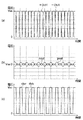
図3は、上記DCオフセット除去回路を動作させなかった場合に、図2の所定の端子に印加される電圧波形の一例を示す図であり、図4は、図3の状態で、上記DCオフセット除去回路を動作させた場合に、図2の所定の端子に印加される電圧波形を示す図である。
【0025】
図3と図4を比較すれば分かるように、上記DCオフセット除去回路を動作させることにより、パルス幅変調出力のデューティ誤差は減少し((c))、パルス幅変調出力に含まれるDCオフセットは除去される((b))。
【0026】
なお、本実施の形態では、BTL出力回路を備えたパルス幅変調増幅器を例に挙げて説明したが、本発明はこれに限定されるわけではなく、通常のパルス幅変調増幅器に対しても同様に適用することができる。
【0027】
図5は、通常のパルス幅変調増幅器に設けたDCオフセット除去回路の一例を示す図である。同図において、図2と異なる点は、コンパレータCMPによって、Lchパルス幅変調増幅部1′からのパルス幅変調出力のレベルとグランド電位とを比較させていることである。これにより、コンパレータCMPは、前記図2と同様に、パルス幅変調増幅部1′からのパルス幅変調出力と同じ形状のパルス列であって、その信号レベルを低下させたもの、つまりデューティパルスを生成している。他の構成および作用は、図2に記載のものと異ならないので、その説明を省略する。
【0028】
このように、本実施の形態では、パルス幅変調出力を比較し、この比較結果を積分し、この積分結果を入力信号に加算するだけで、パルス幅変調出力に含まれるDCオフセットを除去することができるので、少ない部品点数でDCオフセット除去回路を構成でき、これにより、製造コストを低減させながらパルス幅変調出力に含まれるDCオフセットを除去することができる。
【0029】
【発明の効果】
以上説明したように、請求項1または2に記載の発明によれば、パルス幅変調増幅信号のレベルの比較、その比較結果の積分およびその積分結果に応じたDCオフセットの除去という簡単な構成で、パルス幅変調増幅信号に含まれるDCオフセットを除去することができるので、製造コストを低減させながらパルス幅変調出力に含まれるDCオフセットを除去することができる。
【図面の簡単な説明】
【図1】 本発明の一実施の形態に係るパルス幅変調増幅器の全体構成を示すブロック図である。
【図2】 図1のLchパルス幅変調増幅部からのパルス幅変調出力に含まれるDCオフセットを除去するDCオフセット除去回路の構成の一例を示す図である。
【図3】 図2のDCオフセット除去回路を動作させなかった場合に、図2の所定の端子に印加される電圧波形の一例を示す図である。
【図4】 図3の状態で、図2のDCオフセット除去回路を動作させた場合に、図2の所定の端子に印加される電圧波形を示す図である。
【図5】 通常のパルス幅変調増幅器に設けたDCオフセット除去回路の一例を示す図である。
【符号の説明】
1 Lchパルス幅変調増幅部,3 三角波発生器,4 積分回路,5 加算器,12 パルス変調(PWM)部,13 MOSドライバ,PNM1,PPM1,PNM2,PPM2 電界効果トランジスタ,CMP コンパレータ[0001]
BACKGROUND OF THE INVENTION
The present invention relates to a pulse width modulation amplifier in which a DC (direct current) offset included in a pulse width modulation output is removed.
[0002]
[Prior art]
DC offset included in the pulse width modulation output, that is, unnecessary DC component included in the pulse width modulation output generated by pulse width modulation amplification of the input signal whose DC level is not included in the time average value of the signal level. Pulse width modulation amplifiers that have been eliminated are conventionally known.
[0003]
As such a pulse width modulation amplifier, the DC offset included in the pulse width modulation output is detected, and the detection result is fed back to the sawtooth generator side used to generate the pulse width modulation signal as an error signal, There is one in which the direct current level of the sawtooth wave generated by the sawtooth wave generator is changed in accordance with the level of the error signal (see, for example, Patent Document 1).
[0004]
[Patent Document 1]
Japanese Patent Publication No. 2-60089 [0005]
[Problems to be solved by the invention]
However, in the conventional pulse width modulation amplifier, when the error signal is detected, the time average of the pulse width modulation output is detected, and the peak-to-peak level of the pulse width modulation output is detected. A difference from 1/2 of the level is taken as an error signal, and a large number of circuits are required just to detect the error signal. Furthermore, when this error signal is fed back to the sawtooth generator side, a low-pass filter (LPF), a DC amplifier and an adder are used, which increases the manufacturing cost.
[0006]
The present invention has been made paying attention to this point, and it is an object of the present invention to provide a pulse width modulation amplifier capable of removing a DC offset included in a pulse width modulation output while reducing manufacturing costs. To do.
[0007]
[Means for Solving the Problems]
To achieve the above object, a pulse width modulation amplifier according to claim 1 is provided with a BTL output circuit, and outputs two pulse width modulation amplification signals from the BTL output circuit based on an input signal. , Comparing the level of each pulse width modulation amplified signal including a DC offset to generate a duty pulse, and integrating the duty pulse to output a signal of a level proportional to the DC offset and integration means, by combining the signals output by said integrating means to the input signal, possess a removing means for removing a DC offset included in the pulse width modulation amplifier signal, the integrating means is a low pass filter characterized in that it consists of.
[0008]
In order to achieve the above object, the pulse width modulation amplifier according to
[0009]
DETAILED DESCRIPTION OF THE INVENTION
Hereinafter, embodiments of the present invention will be described in detail with reference to the drawings.
[0010]
FIG. 1 is a block diagram showing an overall configuration of a pulse width modulation amplifier according to an embodiment of the present invention.
[0011]
As shown in the figure, the pulse width modulation amplifier of the present embodiment includes a left channel (Lch) pulse width modulation amplification unit 1 having a BTL (Balanced Transformer Less) output circuit that operates with a single power supply VBB. Similarly, a right channel (Rch) pulse width
[0012]
The Lch pulse width modulation amplifying unit 1 compares the level of the amplified input signal IN with the level of the triangular wave supplied from the triangular wave generator 3 with the input
[0013]
The
[0014]
The pulse width modulation output is supplied from the pulse
[0015]
The first complementary circuit composed of the P-channel field effect transistor PPM1 and the N-channel field effect transistor PNM1 is driven by the pulse width modulation output output from the
[0016]
As shown in FIG. 2, the outputs of the first and second complementary circuits are sent to a first low-pass filter composed of a coil L1 and a capacitor C1 and a second low-pass filter composed of a coil L2 and a capacitor C2. The high frequency component is removed by the first and second low pass filters, respectively, and the load (speaker) R is driven by the outputs of the first and second low pass filters.
[0017]
Since the first and second
[0018]
Further, since the Rch pulse width
[0019]
FIG. 2 is a diagram illustrating an example of a configuration of a DC offset removal circuit that removes a DC offset included in the pulse width modulation output from the Lch pulse width modulation amplification unit 1. In FIG. The low-pass filter and load R are also shown.
[0020]
As shown in the figure, the DC offset removal circuit compares the positive (+) side pulse width modulation output output from the Lch pulse width modulation amplification unit 1 with the negative (−) side pulse width modulation output, A comparator CMP that outputs a voltage of a level according to the comparison result, and an integration circuit 4 comprising, for example, a low-pass filter (LPF) that integrates the output from the comparator CMP and extracts only the DC component contained in the output. The
[0021]
The comparator CMP operates with a power supply voltage VDD (for example, 5 V) that is lower than the power supply voltage VBB of the pulse width modulation amplification unit 1. That is, the comparator CMP compares the pulse width modulation outputs on both sides to generate a pulse train having the same shape as that of the pulse width modulation output and having its signal level lowered, that is, a duty pulse.
[0022]
The integrating circuit 4 smoothes the duty pulse. Here, since the DC offset included in the pulse width modulation output appears as a duty error of the duty pulse, the integration circuit 4 smoothes the duty error. As a result, the integration circuit 4 outputs a signal having a level proportional to the DC offset. The
[0023]
For example, if the pulse width modulation output includes a positive level DC offset, the integration circuit 4 outputs a negative level signal. As a result, the level of the input signal IN decreases, and the duty ratio of the pulse width modulation output on each side is corrected in the decreasing direction. On the other hand, when a negative level DC offset is included in the pulse width modulation output, the operation is the reverse of the above operation.
[0024]
FIG. 3 is a diagram illustrating an example of a voltage waveform applied to the predetermined terminal of FIG. 2 when the DC offset removal circuit is not operated. FIG. 4 is a diagram illustrating the DC offset in the state of FIG. FIG. 3 is a diagram illustrating a voltage waveform applied to a predetermined terminal in FIG. 2 when a removal circuit is operated.
[0025]
As can be seen by comparing FIG. 3 and FIG. 4, by operating the DC offset elimination circuit, the duty error of the pulse width modulation output is reduced ((c)), and the DC offset included in the pulse width modulation output is Is removed ((b)).
[0026]
In this embodiment, the pulse width modulation amplifier provided with the BTL output circuit has been described as an example. However, the present invention is not limited to this, and the same applies to a normal pulse width modulation amplifier. Can be applied to.
[0027]
FIG. 5 is a diagram showing an example of a DC offset removal circuit provided in a normal pulse width modulation amplifier. In this figure, the difference from FIG. 2 is that the level of the pulse width modulation output from the Lch pulse width modulation amplification unit 1 ′ is compared with the ground potential by the comparator CMP. As a result, the comparator CMP generates a pulse train having the same shape as the pulse width modulation output from the pulse width modulation amplification unit 1 ′, with its signal level lowered, that is, a duty pulse, as in FIG. is doing. Other configurations and operations are not different from those shown in FIG.
[0028]
As described above, in this embodiment, the pulse width modulation output is compared, the comparison result is integrated, and the integration result is added to the input signal, thereby removing the DC offset included in the pulse width modulation output. Therefore, the DC offset removal circuit can be configured with a small number of parts, and thereby the DC offset included in the pulse width modulation output can be removed while reducing the manufacturing cost.
[0029]
【The invention's effect】
As described above, according to the first or second aspect of the invention, the level of the pulse width modulation amplification signal is compared, the integration of the comparison result and the DC offset removal according to the integration result are eliminated. Since the DC offset included in the pulse width modulation amplification signal can be removed, the DC offset included in the pulse width modulation output can be removed while reducing the manufacturing cost.
[Brief description of the drawings]
FIG. 1 is a block diagram showing an overall configuration of a pulse width modulation amplifier according to an embodiment of the present invention.
2 is a diagram illustrating an example of a configuration of a DC offset removal circuit that removes a DC offset included in a pulse width modulation output from an Lch pulse width modulation amplification unit in FIG. 1;
3 is a diagram illustrating an example of a voltage waveform applied to a predetermined terminal of FIG. 2 when the DC offset removal circuit of FIG. 2 is not operated.
4 is a diagram illustrating a voltage waveform applied to a predetermined terminal in FIG. 2 when the DC offset removal circuit in FIG. 2 is operated in the state of FIG. 3;
FIG. 5 is a diagram showing an example of a DC offset removal circuit provided in a normal pulse width modulation amplifier.
[Explanation of symbols]
1 Lch pulse width modulation amplification unit, 3 triangular wave generator, 4 integration circuit, 5 adder, 12 pulse modulation (PWM) unit, 13 MOS driver, PNM1, PPM1, PNM2, PPM2 field effect transistor, CMP comparator
Claims (2)
DCオフセットを含む前記各パルス幅変調増幅信号のレベルを比較することにより、デューティパルスを生成する比較手段と、
前記デューティパルスを積分することにより、前記DCオフセットに比例したレベルの信号を出力する積分手段と、
前記積分手段によって出力された信号を前記入力信号に合成することにより、前記パルス幅変調増幅信号に含まれるDCオフセットを除去する除去手段と
を有し、
前記積分手段はロウパスフィルタからなることを特徴とするパルス幅変調増幅器。In a pulse width modulation amplifier that includes a BTL output circuit and outputs two pulse width modulation amplification signals from the BTL output circuit based on an input signal,
Comparing means for generating a duty pulse by comparing the level of each pulse width modulated amplified signal including a DC offset;
An integrating means for outputting a signal having a level proportional to the DC offset by integrating the duty pulse;
By combining the signals output by said integrating means to the input signal, possess a removing means for removing a DC offset included in the pulse width modulation amplifier signal,
2. The pulse width modulation amplifier according to claim 1, wherein the integrating means comprises a low pass filter .
DCオフセットを含む前記パルス幅変調増幅信号のレベルを所定値と比較することにより、デューティパルスを生成する比較手段と、
前記デューティパルスを積分することにより、前記DCオフセットに比例したレベルの信号を出力する積分手段と、
前記積分手段によって出力された信号を前記入力信号に合成することにより、前記パルス幅変調増幅信号に含まれるDCオフセットを除去する除去手段と
を有し、
前記積分手段はロウパスフィルタからなることを特徴とするパルス幅変調増幅器。In a pulse width modulation amplifier that outputs a pulse width modulation amplification signal based on an input signal,
Comparing means for generating a duty pulse by comparing the level of the pulse width modulated amplified signal including a DC offset with a predetermined value;
An integrating means for outputting a signal having a level proportional to the DC offset by integrating the duty pulse;
By combining the signals output by said integrating means to the input signal, possess a removing means for removing a DC offset included in the pulse width modulation amplifier signal,
2. The pulse width modulation amplifier according to claim 1, wherein the integrating means comprises a low pass filter .
Priority Applications (1)
| Application Number | Priority Date | Filing Date | Title |
|---|---|---|---|
| JP2002377818A JP4016833B2 (en) | 2002-12-26 | 2002-12-26 | Pulse width modulation amplifier |
Applications Claiming Priority (1)
| Application Number | Priority Date | Filing Date | Title |
|---|---|---|---|
| JP2002377818A JP4016833B2 (en) | 2002-12-26 | 2002-12-26 | Pulse width modulation amplifier |
Publications (2)
| Publication Number | Publication Date |
|---|---|
| JP2004208216A JP2004208216A (en) | 2004-07-22 |
| JP4016833B2 true JP4016833B2 (en) | 2007-12-05 |
Family
ID=32814875
Family Applications (1)
| Application Number | Title | Priority Date | Filing Date |
|---|---|---|---|
| JP2002377818A Expired - Fee Related JP4016833B2 (en) | 2002-12-26 | 2002-12-26 | Pulse width modulation amplifier |
Country Status (1)
| Country | Link |
|---|---|
| JP (1) | JP4016833B2 (en) |
Families Citing this family (5)
| Publication number | Priority date | Publication date | Assignee | Title |
|---|---|---|---|---|
| JP4893201B2 (en) * | 2006-09-28 | 2012-03-07 | 株式会社Jvcケンウッド | Class D amplification apparatus and method |
| GB2496664B (en) * | 2011-11-18 | 2016-03-23 | Cirrus Logic Int Semiconductor Ltd | Amplifier circuit with offset control |
| US9019012B2 (en) | 2011-11-18 | 2015-04-28 | Cirrus Logic International (Uk) Limited | Amplifier circuit with offset control |
| JP5547217B2 (en) | 2012-01-25 | 2014-07-09 | 株式会社東芝 | Amplifier circuit |
| JP5936975B2 (en) * | 2012-09-28 | 2016-06-22 | 新日本無線株式会社 | Class D amplifier circuit |
-
2002
- 2002-12-26 JP JP2002377818A patent/JP4016833B2/en not_active Expired - Fee Related
Also Published As
| Publication number | Publication date |
|---|---|
| JP2004208216A (en) | 2004-07-22 |
Similar Documents
| Publication | Publication Date | Title |
|---|---|---|
| US7142050B2 (en) | Recovery from clipping events in a class D amplifier | |
| JP3941443B2 (en) | Self-propelled PWM amplifier | |
| US8378745B2 (en) | Current sensing | |
| US6998911B2 (en) | Gate control circuit with soft start/stop function | |
| JP4015648B2 (en) | Class D amplifier | |
| JP2000165154A (en) | Peak current limit detecting circuit and class d amplifier with load impedance detecting circuit | |
| JP2003115730A (en) | Pwm (pulse-width modulation) circuit and power amplifier circuit | |
| US9461589B2 (en) | Asymmetric H-bridge in a class D power amplifier | |
| US6476674B2 (en) | Method and apparatus for error correction of amplifier | |
| US20090289705A1 (en) | Pulse modulation type electric power amplifier | |
| JPWO2004010575A1 (en) | Power amplifier device | |
| JP4853176B2 (en) | Class D amplifier | |
| TWM365017U (en) | D-class amplifier | |
| JP4016833B2 (en) | Pulse width modulation amplifier | |
| EP0644649B1 (en) | A pulse width modulation amplifier | |
| EP1887830A2 (en) | Protection circuit and load current detection circuit | |
| US10819293B2 (en) | Power amplifier | |
| US9647612B2 (en) | Power amplifying apparatus and power amplifying method | |
| KR100770747B1 (en) | Digital amplifier and method of reproducing sound | |
| JP2007209038A (en) | Power amplifier circuit | |
| JP4281004B2 (en) | PWM power amplifier and control method thereof | |
| JP3102781B2 (en) | Pulse width modulation amplifier circuit | |
| JP3124179B2 (en) | Pulse width modulation circuit | |
| JP4533707B2 (en) | Amplifier device, power supply circuit for amplifier, and audio signal reproducing device | |
| CN213754451U (en) | Class D amplifier with filter circuit |
Legal Events
| Date | Code | Title | Description |
|---|---|---|---|
| A621 | Written request for application examination |
Free format text: JAPANESE INTERMEDIATE CODE: A621 Effective date: 20050728 |
|
| RD03 | Notification of appointment of power of attorney |
Free format text: JAPANESE INTERMEDIATE CODE: A7423 Effective date: 20060424 |
|
| A131 | Notification of reasons for refusal |
Free format text: JAPANESE INTERMEDIATE CODE: A131 Effective date: 20060801 |
|
| A521 | Written amendment |
Free format text: JAPANESE INTERMEDIATE CODE: A523 Effective date: 20061002 |
|
| A02 | Decision of refusal |
Free format text: JAPANESE INTERMEDIATE CODE: A02 Effective date: 20070403 |
|
| A521 | Written amendment |
Free format text: JAPANESE INTERMEDIATE CODE: A523 Effective date: 20070606 |
|
| A911 | Transfer of reconsideration by examiner before appeal (zenchi) |
Free format text: JAPANESE INTERMEDIATE CODE: A911 Effective date: 20070612 |
|
| TRDD | Decision of grant or rejection written | ||
| A01 | Written decision to grant a patent or to grant a registration (utility model) |
Free format text: JAPANESE INTERMEDIATE CODE: A01 Effective date: 20070828 |
|
| A61 | First payment of annual fees (during grant procedure) |
Free format text: JAPANESE INTERMEDIATE CODE: A61 Effective date: 20070910 |
|
| R150 | Certificate of patent or registration of utility model |
Free format text: JAPANESE INTERMEDIATE CODE: R150 |
|
| FPAY | Renewal fee payment (event date is renewal date of database) |
Free format text: PAYMENT UNTIL: 20100928 Year of fee payment: 3 |
|
| FPAY | Renewal fee payment (event date is renewal date of database) |
Free format text: PAYMENT UNTIL: 20100928 Year of fee payment: 3 |
|
| FPAY | Renewal fee payment (event date is renewal date of database) |
Free format text: PAYMENT UNTIL: 20110928 Year of fee payment: 4 |
|
| FPAY | Renewal fee payment (event date is renewal date of database) |
Free format text: PAYMENT UNTIL: 20120928 Year of fee payment: 5 |
|
| FPAY | Renewal fee payment (event date is renewal date of database) |
Free format text: PAYMENT UNTIL: 20130928 Year of fee payment: 6 |
|
| LAPS | Cancellation because of no payment of annual fees |