JP4012158B2 - Electron microscope apparatus and electron microscope observation method - Google Patents
Electron microscope apparatus and electron microscope observation method Download PDFInfo
- Publication number
- JP4012158B2 JP4012158B2 JP2004036328A JP2004036328A JP4012158B2 JP 4012158 B2 JP4012158 B2 JP 4012158B2 JP 2004036328 A JP2004036328 A JP 2004036328A JP 2004036328 A JP2004036328 A JP 2004036328A JP 4012158 B2 JP4012158 B2 JP 4012158B2
- Authority
- JP
- Japan
- Prior art keywords
- sample
- contrast material
- electron microscope
- sample holder
- contrast
- Prior art date
- Legal status (The legal status is an assumption and is not a legal conclusion. Google has not performed a legal analysis and makes no representation as to the accuracy of the status listed.)
- Expired - Fee Related
Links
Images


Description
この発明は、薄片化した観察領域について、観察面の2次電子発生効率を向上させて走査電子顕微鏡観察を行うための電子顕微鏡装置および電子顕微鏡観察方法に関するものである。 The present invention relates to an electron microscope apparatus and an electron microscope observation method for performing observation with a scanning electron microscope by improving the efficiency of secondary electron generation on an observation surface for a thinned observation region.
図25に従来の観察試料の電子顕微鏡観察方法を示す(例えば、非特許文献1参照)。 FIG. 25 shows a conventional electron microscope observation method of an observation sample (see, for example, Non-Patent Document 1).
例えば、Si基板103上に半導体デバイスパターン104を形成したSi半導体デバイス試料の断面および内部構造を観察するため観察領域102を露出させるように集束イオンビームで例えば約1μmまで薄片化し、電子顕微鏡用試料101を作製する。
For example, in order to observe the cross section and internal structure of the Si semiconductor device sample in which the
次に、この観察領域102を含む電子顕微鏡用試料101について、高加速(例えば、200kV)走査電子顕微鏡像(以下、走査電子顕微鏡をSEMと省略)観察機能と走査透過電子顕微鏡像(以下、走査透過電子顕微鏡をSTEMと省略)観察機能とを備えて構成されるSTEM装置において、観察領域に電子線105を走査して上記試料101のSEMによる断面観察およびSTEMによる内部の構造を観察する。
上記従来の電子顕微鏡観察では、試料内部の構造が微細化、緻密化して詳細なSEMによる断面およびSTEMによる内部の構造観察を行う場合に、観察領域において更に薄膜化する必要がある。ところが、例えば約0.1μmまで薄片化した場合に、観察面の膜厚が薄いために電子線が透過し、観察面から発生する2次電子量が少なくなり、さらに、上記Si半導体デバイスのように導電性を示さない材料も含んで構成される試料の場合には、電子線を照射することにより観察試料表面に電子が帯電するチャージング現象が生じるために、断面観察の際に十分な2次電子を検出することが出来ず、高解像度での断面観察を行うことが困難であった。 In the conventional electron microscope observation, when the structure inside the sample is refined and densified and a detailed cross section by SEM and internal structure observation by STEM are performed, it is necessary to further reduce the film thickness in the observation region. However, for example, when thinned to about 0.1 μm, since the film thickness of the observation surface is thin, the electron beam is transmitted and the amount of secondary electrons generated from the observation surface is reduced. In the case of a sample that also includes a material that does not exhibit conductivity, a charging phenomenon occurs in which electrons are charged on the surface of the observation sample by irradiating an electron beam. Secondary electrons could not be detected, and it was difficult to observe the cross section at high resolution.
また、試料の構造が微細化、緻密化している場合に、薄膜化した観察領域の2つの観察面において、互いに異なる断面構造をもつことがある。この場合には、STEM像は試料の膜厚の厚みで積算された像であるため、試料の構造の詳細を得るためには、SEMによる段面観察を行う必要があるが、上記試料の詳細な断面観察を行う場合には、集束イオンビーム加工装置(以下、FIBと省略)に試料を挿入し、観察領域において観察方向と反対側にFIBによるWなどの金属膜を堆積させるなどの追加加工により2次電子発生効率を向上させる必要があったが(例えば、特許文献1を参照)、上記観察領域は高解像度のSTEM像観察を行うのに十分が薄さに薄片化されているため、FIBによる追加加工により観察領域を破損する危険性を伴うものであった。 Further, when the structure of the sample is miniaturized and densified, the two observation surfaces in the thinned observation region may have different cross-sectional structures. In this case, since the STEM image is an image integrated by the thickness of the sample film, in order to obtain details of the sample structure, it is necessary to perform step surface observation with SEM. When performing simple cross-sectional observation, additional processing such as inserting a sample into a focused ion beam processing apparatus (hereinafter abbreviated as FIB) and depositing a metal film such as W by FIB on the opposite side of the observation direction in the observation region (See, for example, Patent Document 1) , but the observation region is thin enough to perform high-resolution STEM image observation. There was a risk of damaging the observation area by additional processing with FIB.
したがって、この発明の目的は、上記課題に鑑みてなされたものであり、STEM観察が可能な膜厚に薄片化された試料について、観察面の2次電子発生効率を高める機能を備えて高分解能の走査電子顕微鏡観察することが出来る電子顕微鏡装置および電子顕微鏡観察方法を提供することである。 Accordingly, an object of the present invention is made in view of the above problems, and a high-resolution image having a function of increasing the efficiency of generating secondary electrons on the observation surface of a sample thinned to a film thickness enabling STEM observation. It is to provide an electron microscope apparatus and an electron microscope observation method that can be observed with a scanning electron microscope.
上記課題を解決するためにこの発明の請求項1記載の電子顕微鏡装置は、走査電子顕微鏡観察または走査透過電子顕微鏡観察を行うための試料を装着する試料ホルダーと、電子線を照射した際に2次電子発生効率が高く導電性を示すタングステンで構成されたコントラスト材と、前記コントラスト材を駆動するためのコントラスト材駆動部とを備え、前記試料ホルダーは、集束イオンビーム加工装置と走査透過電子顕微鏡装置に共用可能であり、前記試料ホルダーの先端部に設けた試料ステージに前記試料を装着する装着材と前記コントラスト材を配置し、前記試料ホルダーの基端部に、前記試料ホルダーの先端部の向きを変えるための切り替えダイヤルと前記コントラスト材駆動部とを配置しており、前記コントラスト材は、前記試料における電子線が照射される表面側とは反対の裏面側の所定領域に、前記コントラスト材駆動部を制御することによって配置され、前記試料ホルダーの試料ステージに、前記試料が位置する開口部と前記コントラスト材の動作範囲を制限する空間とが設けられ、前記コントラスト材の軸端部の一方に、金属ベルトまたは金属ワイヤの一端を巻きつけて固定するプーリが設けられ、前記金属ベルトまたは金属ワイヤの他端は前記試料ステージの駆動用軸に固定され、前記駆動用軸と前記プーリの間には、前記金属ベルトまたは金属ワイヤを押さえる押さえローラが設けられ、前記コントラスト材の軸端部の他方にコイルばねまたは渦巻きばねが設けられている。
In order to solve the above problems, an electron microscope apparatus according to
請求項2記載の電子顕微鏡装置は、請求項1記載の電子顕微鏡装置において、前記試料ホルダーは、前記コントラスト材駆動部を駆動することによって、前記駆動用軸とともに前記金属ベルトまたは金属ワイヤを、コイルばねまたは渦巻きばねの引力と逆方向に回転力をかけて引き、前記コントラスト材が試料観察面の下に位置するように、前記試料ステージ開口部と前記試料ステージ内部の空間との範囲で前記コントラスト材を駆動する機構を備えている。
The electron microscope apparatus according to
請求項3記載の電子顕微鏡装置は、走査電子顕微鏡観察または走査透過電子顕微鏡観察を行うための試料を装着する試料ホルダーと、電子線を照射した際に2次電子発生効率が高く導電性を示すタングステンで構成されたコントラスト材と、前記コントラスト材を駆動するためのコントラスト材駆動部とを備え、前記試料ホルダーは、集束イオンビーム加工装置と走査透過電子顕微鏡装置に共用可能であり、前記試料ホルダーの先端部に設けた試料ステージに前記試料を装着する装着材と前記コントラスト材を配置し、前記試料ホルダーの基端部に、前記試料ホルダーの先端部の向きを変えるための切り替えダイヤルと前記コントラスト材駆動部とを配置しており、前記コントラスト材は、前記試料における電子線が照射される表面側とは反対の裏面側の所定領域に、前記コントラスト材駆動部を制御することによって配置され、前記試料として、メッシュに張り合わせた透過電子顕微鏡用試料を用い、前記試料ホルダーは、前記試料のメッシュ側を前記試料ステージに載せて前記メッシュを前記装着材と試料ステージとで挟んで装着するように構成され、前記試料が前記電子線と対向するように前記試料ホルダーを電子顕微鏡に挿入することによって、前記試料における前記電子線が照射される表面側とは反対の裏面側において前記コントラスト材が配置されるように駆動する。
The electron microscope apparatus according to
請求項4記載の電子顕微鏡装置は、走査電子顕微鏡観察または走査透過電子顕微鏡観察を行うための試料を装着する試料ホルダーと、電子線を照射した際に2次電子発生効率が高く導電性を示すタングステンで構成されたコントラスト材と、前記コントラスト材を駆動するためのコントラスト材駆動部とを備え、前記試料ホルダーは、集束イオンビーム加工装置と走査透過電子顕微鏡装置に共用可能であり、前記試料ホルダーの先端部に設けた試料ステージに前記試料を装着する装着材と前記コントラスト材を配置し、前記試料ホルダーの基端部に、前記試料ホルダーの先端部の向きを変えるための切り替えダイヤルと前記コントラスト材駆動部とを配置しており、前記コントラスト材は、前記試料における電子線が照射される表面側とは反対の裏面側の所定領域に、前記コントラスト材駆動部を制御することによって配置され、前記試料ホルダーは、前記試料ステージに試料を任意の位置に装着するための装着材と二つのコントラスト材を配置して構成されており、前記試料ホルダーの試料ステージに備えた装着材は、十分な強度をもった金属材から形成され、平坦な試料ステージ上に間隔をあけて互いに対向して試料ステージ開口部の中央側へ一段突き出た当接面が形成された二つの第1装着材と、一端が前記試料ステージに固定された金属ばねを有しかつ十分な強度をもった平坦な金属材からなる第2装着材とが互いに向かい合って配置され、前記金属ばねにより前記第2装着材が試料挿入方向に伸縮運動する。 The electron microscope apparatus according to claim 4 has a sample holder for mounting a sample for observation with a scanning electron microscope or a scanning transmission electron microscope, a high secondary electron generation efficiency when irradiated with an electron beam, and exhibits conductivity. A contrast material composed of tungsten; and a contrast material driving unit for driving the contrast material, wherein the sample holder can be shared by a focused ion beam processing apparatus and a scanning transmission electron microscope apparatus. The mounting material for mounting the sample and the contrast material are arranged on a sample stage provided at the distal end of the sample holder, a switching dial for changing the orientation of the distal end of the sample holder and the contrast at the base end of the sample holder The contrast material is opposite to the surface side of the sample irradiated with the electron beam. Is arranged by controlling the contrast material driving unit in a predetermined area on the back surface side of the sample holder, and the sample holder is arranged with a mounting material for mounting the sample at an arbitrary position on the sample stage and two contrast materials. The mounting material provided for the sample stage of the sample holder is formed of a metal material having sufficient strength, and is opposed to each other with a space on the flat sample stage. A second metal member comprising a first metal member having a contact surface projecting one step toward the center and a flat metal member having a metal spring having one end fixed to the sample stage and sufficient strength. The mounting material is disposed so as to face each other, and the second mounting material expands and contracts in the sample insertion direction by the metal spring.
請求項5記載の電子顕微鏡装置は、請求項4記載の電子顕微鏡装置において、前記第1装着材と試料ステージに、前記二つのコントラスト材それぞれが互いに衝突せずに駆動させるための二つの空洞とそれらの間に金属板を備えている。 The electron microscope apparatus according to claim 5 is the electron microscope apparatus according to claim 4 , wherein the first mounting material and the sample stage have two cavities for driving the two contrast materials without colliding with each other. A metal plate is provided between them.
請求項6記載の電子顕微鏡装置は、走査電子顕微鏡観察または走査透過電子顕微鏡観察を行うための試料を装着する試料ホルダーと、電子線を照射した際に2次電子発生効率が高く導電性を示すタングステンで構成されたコントラスト材と、前記コントラスト材を駆動するためのコントラスト材駆動部とを備え、前記試料ホルダーは、集束イオンビーム加工装置と走査透過電子顕微鏡装置に共用可能であり、前記試料ホルダーの先端部に設けた試料ステージに前記試料を装着する装着材と前記コントラスト材を配置し、前記試料ホルダーの基端部に、前記試料ホルダーの先端部の向きを変えるための切り替えダイヤルと前記コントラスト材駆動部とを配置しており、前記コントラスト材は、前記試料における電子線が照射される表面側とは反対の裏面側の所定領域に、前記コントラスト材駆動部を制御することによって配置され、前記試料ホルダーは、前記試料ステージに試料を任意の位置に装着するための装着材と二つのコントラスト材を配置して構成されており、前記試料ホルダーの二つのコントラスト材は、常時コントラスト材の駆動方向と逆方向に力を加えるために、前記試料ステージ内部の固定された部位に取り付けられた金属ばねと、減速ギヤとマイクロメータとを有する前記コントラスト材駆動部に取り付けられた金属ワイヤとをそれぞれ備え、前記コントラスト材駆動部のマイクロメータを回転させ、減速ギヤと金属ワイヤを介して前記コントラスト材を駆動させる。 The electron microscope apparatus according to claim 6 has a sample holder for mounting a sample for observation with a scanning electron microscope or a scanning transmission electron microscope, a high secondary electron generation efficiency when irradiated with an electron beam, and conductivity. A contrast material composed of tungsten; and a contrast material driving unit for driving the contrast material, wherein the sample holder can be shared by a focused ion beam processing apparatus and a scanning transmission electron microscope apparatus. The mounting material for mounting the sample and the contrast material are arranged on a sample stage provided at the distal end of the sample holder, a switching dial for changing the orientation of the distal end of the sample holder and the contrast at the base end of the sample holder The contrast material is opposite to the surface side of the sample irradiated with the electron beam. Is arranged by controlling the contrast material driving unit in a predetermined area on the back surface side of the sample holder, and the sample holder is arranged with a mounting material for mounting the sample at an arbitrary position on the sample stage and two contrast materials. The two contrast members of the sample holder are composed of a metal spring attached to a fixed part inside the sample stage and a speed reducer in order to apply a force in the direction opposite to the driving direction of the contrast material at all times. A metal wire attached to the contrast material driving unit having a gear and a micrometer is provided, respectively, and the micrometer of the contrast material driving unit is rotated to drive the contrast material via the reduction gear and the metal wire.
請求項7記載の電子顕微鏡装置は、走査電子顕微鏡観察または走査透過電子顕微鏡観察を行うための試料を装着する試料ホルダーと、電子線を照射した際に2次電子発生効率が高く導電性を示すタングステンで構成されたコントラスト材と、前記コントラスト材を駆動するためのコントラスト材駆動部とを備え、前記試料ホルダーは、集束イオンビーム加工装置と走査透過電子顕微鏡装置に共用可能であり、前記試料ホルダーの先端部に設けた試料ステージに前記試料を装着する装着材と前記コントラスト材を配置し、前記試料ホルダーの基端部に、前記試料ホルダーの先端部の向きを変えるための切り替えダイヤルと前記コントラスト材駆動部とを配置しており、前記コントラスト材は、前記試料における電子線が照射される表面側とは反対の裏面側の所定領域に、前記コントラスト材駆動部を制御することによって配置され、前記試料ホルダーは、前記試料ステージに試料を任意の位置に装着するための装着材と二つのコントラスト材を配置して構成されており、前記試料ホルダーに用いる電子顕微鏡用試料は、観察領域を含む部分が凸型に突出した凸部となり、前記凸部の外周部は一様に所定の高さになっており、前記第2装着材が前記試料の底面に当接し、互いに対向した二つの第1装着材に形成された当接面が前記試料の凸部外周部の試料面に当接して、これらの当接面が位置決めストッパーとしての役割を果たしながら、前記試料の凸部外周部の試料面と、前記試料の底面とを挟んで前記試料を常時任意の位置に装着可能とした。
The electron microscope apparatus according to
請求項8記載の電子顕微鏡装置は、ポールピース装着型の走査透過電子顕微鏡を備えた電子顕微鏡装置であって、前記走査透過電子顕微鏡観察を行うための試料を装着する試料ホルダーと、電子線を照射した際に2次電子発生効率が高く導電性を示すタングステンで構成された二つのコントラスト材と、前記コントラスト材を駆動するための二つのコントラスト材駆動部とを備え、前記コントラスト材は、前記試料における電子線が照射される表面側とは反対の裏面側の所定領域に、前記コントラスト材駆動部を制御することによって配置され、前記二つのコントラスト材は、前記電子顕微鏡試料の薄片化していない周辺部の試料膜厚の影響を受けないために前記試料の薄片領域よりも小さい幅で、かつ薄片化されてない試料周辺部を損傷しない大きさの金属板で構成され、観察面の反対側の面から所定の距離をもつ高さに前記コントラスト材が設置される。 The electron microscope apparatus according to claim 8 is an electron microscope apparatus provided with a scanning transmission electron microscope of a pole piece mounting type, a sample holder for mounting a sample for performing the scanning transmission electron microscope observation, and an electron beam. Two contrast materials composed of tungsten having high secondary electron generation efficiency when irradiated, and two contrast material driving portions for driving the contrast material, It is arranged by controlling the contrast material driving unit in a predetermined region on the back surface side opposite to the front surface side irradiated with the electron beam in the sample, and the two contrast materials are not thinned of the electron microscope sample. In order not to be affected by the sample film thickness in the peripheral part, the width of the sample is smaller than the thin piece region, and the peripheral part of the sample that has not been thinned is damaged. Consists in the stomach size of the metal plate, the contrast material is placed at a height from the surface opposite of the viewing surface having a predetermined distance.
請求項9記載の電子顕微鏡装置は、ポールピース装着型の走査透過電子顕微鏡を備えた電子顕微鏡装置であって、前記走査透過電子顕微鏡観察を行うための試料を装着する試料ホルダーと、電子線を照射した際に2次電子発生効率が高く導電性を示すタングステンで構成された二つのコントラスト材と、前記コントラスト材を駆動するための二つのコントラスト材駆動部とを備え、前記コントラスト材は、前記試料における電子線が照射される表面側とは反対の裏面側の所定領域に、前記コントラスト材駆動部を制御することによって配置され、前記電子顕微鏡のポールピース内部に備えた前記試料ホルダー先端部が移動できる空間内で、前記二つのコントラスト材は前記試料ホルダーに装着した試料観察面の観察方向と反対側の任意の高さに配置され、前記任意の高さで電子線の入射方向に対して垂直方向にのみ駆動する機能を備えている。 The electron microscope apparatus according to claim 9 is an electron microscope apparatus provided with a scanning transmission electron microscope of a pole piece mounting type, a sample holder for mounting a sample for performing the scanning transmission electron microscope observation, and an electron beam Two contrast materials composed of tungsten having high secondary electron generation efficiency when irradiated, and two contrast material driving portions for driving the contrast material, The sample holder tip disposed inside the pole piece of the electron microscope is disposed in a predetermined region on the back surface side opposite to the front surface side irradiated with the electron beam in the sample by controlling the contrast material driving unit. Within the movable space, the two contrast materials are at an arbitrary height opposite to the observation direction of the sample observation surface mounted on the sample holder. It is disposed, and a function of driving only in the direction perpendicular to the incident direction of the electron beam at the desired height.
この発明の請求項1〜9記載の電子顕微鏡装置によれば、試料ホルダーと、コントラスト材と、コントラスト材駆動部とを備え、コントラスト材は、試料における電子線が照射される表面側とは反対の裏面側の所定領域に、コントラスト材駆動部を制御することによって配置されるので、試料の観察方向と反対側に金属膜を堆積させるなどの再加工を施す工程を省略し、さらに、観察領域を破壊することなく、その観察方向と反対側の試料の薄片化部分に近い位置にコントラスト材を設置した状態で、任意の観察面について電子線を照射し、2次電子発生効率を向上させ、高分解能のSEM観察を行うことが出来る。 According to the electron microscope apparatus of the first to ninth aspects of the present invention, the sample microscope includes the sample holder, the contrast material, and the contrast material driving unit, and the contrast material is opposite to the surface side of the sample irradiated with the electron beam. Since the contrast material driving unit is disposed in a predetermined area on the back surface side of the substrate, a reworking process such as depositing a metal film on the side opposite to the observation direction of the sample is omitted. Without damaging the observation direction, with the contrast material installed at a position close to the thinned portion of the sample opposite to the observation direction, an electron beam is irradiated on an arbitrary observation surface to improve the secondary electron generation efficiency, High-resolution SEM observation can be performed.
また、試料の解析目的に対応させてコントラスト材を用いて2次電子発生効率を向上させた高解像度のSEM像、コントラスト材を用いないSTEM観察を容易に選択し切り替えて観察することが出来るため、薄片化試料の断面および内部の構造についての詳細を得ることが出来る。 In addition, a high-resolution SEM image in which secondary electron generation efficiency is improved using a contrast material in accordance with the analysis purpose of the sample, and STEM observation without using a contrast material can be easily selected and switched for observation. Details about the cross-section and internal structure of the exfoliated sample can be obtained.
また、コントラスト材は、2次電子の発生効率が高くかつ導電性を示す金属からなるので、試料の任意の観察面について、高解像度のSEM像を得る。 Further, since the contrast material is made of a metal having high secondary electron generation efficiency and conductivity, a high-resolution SEM image can be obtained for an arbitrary observation surface of the sample.
請求項1〜7では、試料ホルダーは、集束イオンビーム加工装置と走査透過電子顕微鏡装置に共用可能であり、試料ホルダーの先端部に設けた試料ステージに試料を装着する装着材とコントラスト材を配置し、試料ホルダーの基端部に、試料ホルダーの先端部の向きを変えるための切り替えダイヤルとコントラスト材駆動部とを配置しているので、試料ホルダーは集束イオンビーム加工装置と走査透過電子顕微鏡装置の試料ホルダーと共用できる。また、試料ホルダーの基端部に設けた切り替えダイヤルにより試料ホルダーの先端部のみを回転させることができ、またコントラスト材駆動部によりコントラスト材の駆動を行うことでSEM観察を行うことができる。 In claims 1-7, the sample holder is capable shared scanning transmission electron microscope and a focused ion beam processing apparatus, arranged mounting member and contrast material for mounting a sample on a sample stage provided at the tip of the sample holder In addition, since a switching dial for changing the direction of the tip of the sample holder and a contrast material driving unit are arranged at the base end of the sample holder, the sample holder is a focused ion beam processing device and a scanning transmission electron microscope device. Can be shared with other sample holders. Further, only the distal end portion of the sample holder can be rotated by a switching dial provided at the base end portion of the sample holder, and SEM observation can be performed by driving the contrast material by the contrast material driving portion.
請求項1では、試料ホルダーの試料ステージに、試料が位置する開口部とコントラスト材の動作範囲を制限する空間とが設けられ、コントラスト材の軸端部の一方に、金属ベルトまたは金属ワイヤの一端を巻きつけて固定するプーリが設けられ、金属ベルトまたは金属ワイヤの他端は試料ステージの駆動用軸に固定され、駆動用軸とプーリの間には、金属ベルトまたは金属ワイヤを押さえる押さえローラが設けられ、また、前記コントラスト材の軸の他方の端部には、コイルばねまたは渦巻きばねが設けられ、コイルばねまた渦巻きばねは、その一端がコントラスト材の軸端部に巻きつけ固定され、反対側は試料ステージのばね取り付け部に固定されており、コントラスト材が試料観察面の下に位置するのと反対側に、常に引力がかかるようになっている。金属ベルトまたは金属ワイヤを試料ホルダーの先端部と基端部とをつなぐ方向、つまり、コイルばねまたは渦巻きばねの引力と逆方向に、回転力をかけることによりコントラスト材を駆動させることができる。 In the first aspect of the present invention , the sample stage of the sample holder is provided with an opening in which the sample is located and a space that limits the operating range of the contrast material, and one end of a metal belt or metal wire is provided on one of the shaft end portions of the contrast material. The other end of the metal belt or wire is fixed to the drive shaft of the sample stage, and a pressing roller for pressing the metal belt or metal wire is provided between the drive shaft and the pulley. A coil spring or a spiral spring is provided at the other end of the contrast material shaft, and one end of the coil spring or spiral spring is wound around and fixed to the contrast material shaft end. The side is fixed to the spring mounting part of the sample stage, so that an attractive force is always applied to the opposite side of the contrast material located under the sample observation surface. Going on. The contrast material can be driven by applying a rotational force in a direction in which the metal belt or the metal wire is connected to the distal end portion and the proximal end portion of the sample holder, that is, in a direction opposite to the attractive force of the coil spring or the spiral spring.
請求項2では、試料ホルダーは、コントラスト材駆動部を駆動することによって、駆動用軸とともに金属ベルトまたは金属ワイヤが前後に動き、試料ステージ開口部と試料ステージ内部の空間との範囲でコントラスト材を駆動する機構を備えているので、コントラスト材駆動部によりコントラスト材を駆動させることができる。 According to a second aspect of the present invention , the sample holder drives the contrast material driving unit so that the metal belt or the metal wire moves back and forth together with the driving shaft, and the contrast material is moved in the range between the sample stage opening and the space inside the sample stage. Since the driving mechanism is provided, the contrast material can be driven by the contrast material driving unit.
請求項3では、試料として、メッシュに張り合わせた透過電子顕微鏡用試料を用い、試料ホルダーは、試料のメッシュ側を試料ステージに載せてメッシュを装着材と試料ステージとで挟んで装着するように構成され、試料が電子線と対向するように試料ホルダーを電子顕微鏡に挿入することによって、試料における電子線が照射される表面側とは反対の裏面側においてコントラスト材が配置されるように駆動するので、メッシュにより試料を試料ステージに装着することができ、SEM観察を行うことができる。 According to a third aspect of the present invention, a sample for a transmission electron microscope bonded to a mesh is used as a sample, and the sample holder is mounted so that the mesh side of the sample is placed on the sample stage and the mesh is sandwiched between the mounting material and the sample stage. Since the sample holder is inserted into the electron microscope so that the sample faces the electron beam, the contrast material is driven on the back side opposite to the surface side irradiated with the electron beam in the sample. the sample can be mounted on the sample stage by the mesh, it is possible to perform SEM observation.
請求項4,6,7では、試料ホルダーは、試料ステージに試料を任意の位置に装着するための装着材と二つ以上のコントラスト材を配置して構成されるので、特に二つの観察面で断面構造が互いに異なる試料の場合に、所望の観察領域について2方向から詳細にSEM観察を行うことが出来る。 In the fourth , sixth , and seventh aspects , since the sample holder is configured by arranging a mounting material for mounting the sample at an arbitrary position and two or more contrast materials on the sample stage, two specimens are used. In the case of samples having different cross-sectional structures, it is possible to perform SEM observation in detail from two directions for a desired observation region.
請求項4では、試料ホルダーの試料ステージに備えた装着材は、十分な強度をもった金属材から形成され、平坦な試料ステージ上に間隔をあけて互いに対向して試料ステージ開口部の中央側へ一段突き出た当接面が形成された二つの第1装着材と、一端が試料ステージに固定された金属ばねを有しかつ十分な強度をもった平坦な金属材からなる第2装着材とが互いに向かい合って配置され、金属ばねにより第2装着材が試料挿入方向に伸縮運動するので、第2装着材を押して試料を載せると、金属ばねの弾力を利用して、試料を二つの第1装着材に押し付けた状態で支持することができる。 According to a fourth aspect of the present invention , the mounting material provided for the sample stage of the sample holder is formed of a metal material having sufficient strength, and is opposed to each other with a space on the flat sample stage so as to face the center side of the sample stage opening. Two first mounting members each formed with a contact surface projecting one step toward the surface, and a second mounting member made of a flat metal material having a metal spring with one end fixed to the sample stage and having sufficient strength; Are arranged so as to face each other, and the second mounting material expands and contracts in the sample insertion direction by the metal spring. Therefore, when the second mounting material is pushed and the sample is loaded, the elasticity of the metal spring is used to place the sample into the two first samples. It can be supported while pressed against the mounting material.
請求項5では、第1装着材と試料ステージに、二つのコントラスト材それぞれが互いに衝突せずに駆動させるための二つの空洞とそれらの間に金属板を備えているので、金属板と空洞に沿ってコントラスト材を平行移動させることができる。 In claim 5 , since the first mounting material and the sample stage are provided with two cavities for driving the two contrast materials without colliding with each other and a metal plate therebetween, the metal plate and the cavity are provided with The contrast material can be translated along.
請求項6では、試料ホルダーの二つのコントラスト材は、常時コントラスト材の駆動方向と逆方向に力を加えるために、試料ステージ内部の固定された部位に取り付けられた金属ばねと、減速ギヤとマイクロメータとを有するコントラスト材駆動部に取り付けられた金属ワイヤとをそれぞれ備え、コントラスト材駆動部のマイクロメータを回転させ、減速ギヤと金属ワイヤを介してコントラスト材を駆動させるので、コントラスト材駆動部により、二つのコントラスト材を平行移動させることができる。 According to a sixth aspect of the present invention , the two contrast members of the sample holder are provided with a metal spring, a reduction gear, and a micro gear attached to a fixed portion inside the sample stage in order to constantly apply a force in the direction opposite to the driving direction of the contrast material. Each having a metal wire attached to a contrast material driving unit having a meter and rotating the micrometer of the contrast material driving unit to drive the contrast material via the reduction gear and the metal wire. The two contrast materials can be translated.
請求項7では、試料ホルダーに用いる電子顕微鏡用試料は、観察領域を含む部分が凸型に突出した凸部となり、凸部の外周部は一様に所定の高さになっているので、凸部の外周部が二つの第1装着材に当接して位置決めされる。また、凸部の観察面の一方または他方の側にコントラスト材を配置することができ、2方向から詳細にSEM観察が可能となる。 According to the seventh aspect of the present invention , the electron microscope sample used for the sample holder has a convex portion in which the portion including the observation region protrudes in a convex shape, and the outer peripheral portion of the convex portion has a uniform height. The outer peripheral part of the part is positioned in contact with the two first mounting materials. Further, a contrast material can be disposed on one or the other side of the observation surface of the convex portion, and SEM observation can be performed in detail from two directions.
また、第2装着材が試料の底面に当接し、互いに対向した二つの第1装着材に形成された当接面が試料の凸部外周部の試料面に当接して、これらの当接面が位置決めストッパーとしての役割を果たしながら、試料の凸部外周部の試料面と、試料の底面とを挟んで試料を常時任意の位置に装着可能としたので、試料を常に任意の寸法で作製し、常に試料ホルダーの任意の位置でかつ試料ホルダー対して平行に試料を装着できる。 Further , the second mounting material contacts the bottom surface of the sample, the contact surfaces formed on the two first mounting materials facing each other contact the sample surface of the outer peripheral portion of the convex portion of the sample, and these contact surfaces While serving as a positioning stopper, the sample can always be mounted at any position with the sample surface on the outer periphery of the convex portion of the sample sandwiched between the bottom surface of the sample. The sample can always be mounted at an arbitrary position of the sample holder and parallel to the sample holder.
請求項8,9では、ポールピース装着型の走査透過電子顕微鏡を備えた電子顕微鏡装置であって、二つ以上のコントラスト材と、コントラスト材を駆動するための二つ以上のコントラスト材駆動部とを備えるので、焦点距離が短くかつ高分解能を可能とするための、対物レンズによる磁界を金属製のポールピースにかけて構成される磁界型電子レンズを備えたポールピース装着型の電子顕微鏡を備えた構成において、二つの観察面で断面構造が互いに異なる試料の場合に、所望の観察領域について2方向から詳細にSEM観察を行うことが出来る。 Claims 8 and 9 are electron microscope apparatuses provided with a scanning transmission electron microscope equipped with a pole piece, wherein two or more contrast materials, and two or more contrast material driving units for driving the contrast materials, A configuration equipped with a pole piece mounting type electron microscope equipped with a magnetic type electron lens configured by applying a magnetic field by an objective lens to a metal pole piece to enable a short focal length and high resolution. In the case of the samples having different cross-sectional structures on the two observation surfaces, the SEM observation can be performed in detail from two directions for the desired observation region.
請求項8では、二つのコントラスト材は、電子顕微鏡試料の薄片化していない周辺部の試料膜厚の影響を受けないために試料の薄片領域よりも小さい幅で、かつ薄片化されてない試料周辺部を損傷しない大きさの金属板で構成され、観察面の反対側の面から所定の距離をもつ高さにコントラスト材が設置されるので、コントラスト材が試料の薄片化していない部分に接触せずかつ試料の薄片化していない周辺領域の試料厚みの影響を受けることなく観察面の反対側に位置するように移動させることができる。 According to claim 8 , the two contrast materials are not affected by the sample film thickness in the peripheral portion of the electron microscope sample that has not been thinned, so that the width of the contrast material is smaller than that of the thin piece region of the sample and is not thinned. Contrast material is installed at a height with a predetermined distance from the surface opposite to the observation surface, so that the contrast material does not touch the unflaked part of the sample. Therefore, the sample can be moved so as to be located on the opposite side of the observation surface without being affected by the sample thickness in the peripheral region where the sample is not thinned.
請求項9では、電子顕微鏡のポールピース内部に備えた試料ホルダー先端部が移動できる空間内で、二つのコントラスト材は試料ホルダーに装着した試料観察面の観察方向と反対側の任意の高さに配置され、任意の高さで電子線の入射方向に対して垂直方向にのみ駆動する機能を備えているので、コントラスト材が観察面に近接した状態でSEM観察を行えば、観察面は観察方向と反対側でのコントラスト材の設置により、2次電子発生効率が向上し、観察面について高解像度のSEM観察を行うことができる。 According to a ninth aspect of the present invention , in the space in which the tip of the sample holder provided in the pole piece of the electron microscope can move, the two contrast materials are at an arbitrary height opposite to the observation direction of the sample observation surface mounted on the sample holder. Since it is arranged and has a function of driving at an arbitrary height only in a direction perpendicular to the incident direction of the electron beam, if the SEM observation is performed with the contrast material close to the observation surface, the observation surface is in the observation direction. The contrast material on the opposite side improves the generation efficiency of secondary electrons and enables high-resolution SEM observation on the observation surface.
この発明の第1の実施形態を図1〜図8に基づいて説明する。 A first embodiment of the present invention will be described with reference to FIGS.
本発明の実施形態1では、試料の観察領域について、任意の1方向で詳細な断面SEM観察を行うことが出来る試料ホルダーおよびそれを用いた電子顕微鏡観察方法を取り上げて説明する。
In
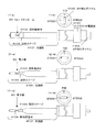
図1は、本発明の実施形態に関わる試料ホルダーH1の概略構成図である。この試料ホルダーH1は、集束イオンビーム加工装置(以下、FIBと省略)と、走査電子顕微鏡(以下、SEMと省略)および走査透過電子顕微鏡(以下、STEMと省略)観察が可能なSTEM装置との共用試料ホルダーであり、図1に示すように試料ホルダーH1は、先端部H101と端部(基端部)H102とで構成され、試料ホルダーH1の先端部H101は試料ステージH103と試料装着材H104で構成され、試料ステージH103はコントラスト材H105とコントラスト材H105の動作範囲についての空洞H103aとその端部に当接面H103bと、コントラスト材H105の軸H114とその軸H114が回転するためのH103cとを備え(図3)、試料ホルダーH1の端部H102は、切り替えダイヤルH106とコントラスト材駆動部H107とを備える。 FIG. 1 is a schematic configuration diagram of a sample holder H1 according to an embodiment of the present invention. This sample holder H1 includes a focused ion beam processing apparatus (hereinafter abbreviated as FIB), a scanning electron microscope (hereinafter abbreviated as SEM) and a scanning transmission electron microscope (hereinafter abbreviated as STEM). As shown in FIG. 1, the sample holder H1 is composed of a front end H101 and an end (base end) H102, and the front end H101 of the sample holder H1 is a sample stage H103 and a sample mounting material H104. The sample stage H103 includes a contrast material H105, a cavity H103a with respect to the operating range of the contrast material H105, an abutting surface H103b at an end thereof, an axis H114 of the contrast material H105, and an H103c for rotating the axis H114. (FIG. 3), the end H102 of the sample holder H1 is provided with a switching dial H1. And a 6 and contrast material driver H107.
次に、試料ホルダーH1の端部H102の切り替えダイヤルH106は、それぞれ図2(1−a,b)、(2−a,b)、(3−a,b)に示すように、FIB、STEM1、STEM2の向きに切り替えダイヤルH106を切り替えると、試料ホルダーH1の先端部H101のみを図に示すように90度ずつ回転させることが出来る。このとき、端部H102のコントラスト材駆動部H107は、切り替えダイヤルH106の向きを切り替えても回転しないが、以下、図7(1−a,2−a)に示すように、FIBおよびSTEM1の向きに回転させることにより、コントラスト材H105を駆動するものとする。また、図2は、それぞれの切り替えダイヤルH106の向きにおいて、FIB内、STEM内での試料ホルダーH1の先端部H101の向きとFIB内のGa+イオンビームB1、STEM内の電子線B2の向きとの関係を示している。 Next, as shown in FIGS. 2 (1-a, b), (2-a, b), (3-a, b), the switching dial H106 of the end portion H102 of the sample holder H1 is FIB, STEM1. When the switching dial H106 is switched to the direction of STEM2, only the tip H101 of the sample holder H1 can be rotated by 90 degrees as shown in the figure. At this time, the contrast material driving unit H107 at the end H102 does not rotate even when the direction of the switching dial H106 is switched. However, as shown in FIG. 7 (1-a, 2-a), the directions of FIB and STEM1 are as follows. It is assumed that the contrast material H105 is driven by rotating it to the right. Further, FIG. 2 shows the orientation of the tip H101 of the sample holder H1 in the FIB and the STEM, the direction of the Ga + ion beam B1 in the FIB, and the electron beam B2 in the STEM in the direction of each switching dial H106. Showing the relationship.
次に、図3,4に示すように、試料ステージH103に備えたコントラスト材H105は、2次電子発生効率が高く導電性を示す金属であるWから構成され、その先端には試料に当たらない程度の大きさ(例えば、1.5mm程度)で、かつ突起の高さが切り欠きメッシュの厚さ(例えば、50μm)相当の平坦な面をもつ突起部H105aを有している。またコントラスト材H105の軸H114には、その軸H114端部の一方に金属ベルトH108とそれを巻きつけ固定するプーリH109とを設けている。金属性ベルトH108はその一端が試料ステージH103のプーリH109に巻きつけ固定され、反対側は試料ステージH103の駆動用軸H110に固定されている。また、軸H114の他方の端部にはコイルばねH113を設けている。コイルばねH113は、その一端が軸H114の端部に巻きつけ固定され、反対側は試料ステージH103に取り付けられた、ばね取り付け部H115に固定されており、コントラスト材H105が当接面H103bに当接するように常に引力がかかるようになっている。 Next, as shown in FIGS. 3 and 4, the contrast material H105 provided in the sample stage H103 is made of W which is a metal having high secondary electron generation efficiency and conductivity, and the tip does not hit the sample. The protrusion H105a has a flat surface corresponding to the size of the protrusion (for example, approximately 1.5 mm) and the height of the protrusion corresponding to the notch mesh thickness (for example, 50 μm). Further, the shaft H114 of the contrast material H105 is provided with a metal belt H108 and a pulley H109 for winding and fixing the belt on one end of the shaft H114. One end of the metallic belt H108 is wound around and fixed to the pulley H109 of the sample stage H103, and the other side is fixed to the driving shaft H110 of the sample stage H103. A coil spring H113 is provided at the other end of the shaft H114. One end of the coil spring H113 is wound around and fixed to the end portion of the shaft H114, and the other side is fixed to a spring mounting portion H115 attached to the sample stage H103. The contrast material H105 contacts the contact surface H103b. Attraction is always applied to touch.
さらに、上記コントラスト材駆動用軸H110と試料ステージH103のプーリH109の間に押さえローラH111を入れ、これで金属ベルトH108の途中を押さえている。なお、コントラスト材105の駆動は、試料ホルダーH1の端部H102のコントラスト材駆動部H107を回転させることにより、金属ベルトH108を試料ホルダーH1の先端部H101と端部H102とをつなぐ方向、つまりコイルばねH113の引力と逆方向に回転力をかけることで行っている。金属ベルトH108の長さにより、コントラスト材105の動作範囲は試料ステージH103の空洞H103aと試料ステージ開口部H112の間で制限されて構成される。従って、試料ホルダーH1をSTEM装置に挿入した状態で、試料ステージH103に備えたコントラスト材駆動部H106を介してコントラスト材H105の位置を変えることが出来る。
Further, a pressing roller H111 is inserted between the contrast material driving shaft H110 and the pulley H109 of the sample stage H103, thereby pressing the middle of the metal belt H108. The
次に、本発明の実施形態1に関わる試料を図5に示す。本実施形態に用いる試料は、Si半導体デバイスであり、図25と同様にSi基板103上に半導体デバイスパターン104を形成し、図5(1)に示すように、L字型の形状にダイシング加工したL字型試料106を、3mmΦの半円型の切り欠きメッシュ107に対してL字型試料106の凸部を接着して作製されている。なお、L字型試料106は、観察する部分である凸部と切り欠きメッシュ107が必ず重ならないようにして切り欠きメッシュ107に接着し、電子顕微鏡用試料を作製する。
Next, a sample according to
次に、図6に示すように、上記L字型試料106は、試料ステージH103側に切り欠きメッシュ107を、試料ホルダーH1の試料装着材H104側に試料観察面108を配置する向きにして、試料ホルダーH1の試料ステージH103と試料装着材H104とでL字型試料106の切り欠きメッシュ107の一部を挟んで装着される。L字型試料106の観察面108を、図5(2)に示すように、FIB加工により、透過電子顕微鏡でも観察可能な任意の膜厚(例えば、0.1μm)に薄片化する。
Next, as shown in FIG. 6, the L-shaped
次に、本発明の実施形態1に関わる電子顕微鏡観察方法の一例について、図7、図8を参照しながら詳細に説明する。ここで、L字型試料106は、図7(1−a,b,c)に示すように、上記試料の観察面108に対して電子線B2を照射することとし、試料ホルダーH1の端部H102の切り替えダイヤルH106をSTEM1の向きに合わせて、STEMに挿入されている。この状態では、コントラスト材H105がコイルばねH113の引力により当接面H103bに当接しているので、SEM観察も、STEM観察もすることが出来る。
Next, an example of the electron microscope observation method according to the first embodiment of the present invention will be described in detail with reference to FIGS. Here, as shown in FIG. 7 (1-a, b, c), the L-shaped
次に、試料ホルダーH1の端部H102に備えたコントラスト材駆動部H107をSTEM1に回転させることにより、図7(2−a,b,c)に示すように、観察面108の観察方向である電子線B2の向きと反対側に設置するように試料ステージの空洞H103aを通ってコントラスト材H105を駆動させる。コントラスト材H105を駆動させて、コントラスト材突起部H105aの面が試料周辺部の面106aに接しながら切り欠きメッシュ107の上面に到達するとコントラスト材H105の駆動は停止する。この図7(2−a,b,c)に示す状態でSEM観察を行えば、薄片化している試料の観察面108は、観察方向と反対側にコントラスト材突起部H105aの設置により、2次電子発生効率が向上し、観察面108のSEM像を高解像度で得ることが出来る。
Next, by rotating the contrast material driving unit H107 provided at the end H102 of the sample holder H1 to the STEM1, the viewing direction of the observation surface 108 is as shown in FIG. 7 (2-a, b, c). The contrast material H105 is driven through the cavity H103a of the sample stage so as to be installed on the side opposite to the direction of the electron beam B2. When the contrast material H105 is driven and the surface of the contrast material projection H105a reaches the upper surface of the
図8に示すように、コントラスト材の突起部H105aが試料の観察面108の周辺にある凸部側壁109に接していれば、観察面108の電子線照射によるチャージング効果も低減することが出来るため、2次電子発生効率向上の効果と合わせて高解像度のSEM観察を行うことが出来る。
As shown in FIG. 8, if the projection H105a of the contrast material is in contact with the
本実施形態1によれば、FIBとの共用可能な走査透過電子顕微鏡用ホルダーの走査電子顕微鏡観察用2次電子発生率向上用のコントラスト材としてWを代表とする金属から構成されるコントラスト材とを組み合わせているので、試料のSTEM装置への入れ替えなしに、かつ観察面と反対側に金属膜を堆積させるなどの追加加工なしに、既存のSTEM装置を用いて、2次電子発生効率を高めて高解像度のSEM観察を行うことが出来る。
また、コントラスト材H105に突起部H105aを備えているのは、観察面108とコントラスト材H105との距離を小さくして2次電子発生効率を向上させるためであり、2次電子発生効率を高めた際の効果を保つためにコントラスト材突起部H105aと試料観察面108との距離を縮めるため、切り欠きメッシュ107と接着剤による距離分を縮めてコントラスト材H105を設置することが出来るようにするためである。コントラスト材の突起部H105aは、L字型試料106の観察面108の周辺部にしか当たらないため、観察面108にコントラスト材H105を衝突させて破損することもない。
According to the first embodiment, a contrast material composed of a metal typified by W as a contrast material for improving the secondary electron generation rate for scanning electron microscope observation of a scanning transmission electron microscope holder that can be shared with FIB Therefore, the efficiency of secondary electron generation can be increased by using an existing STEM device without replacing the sample with the STEM device and without additional processing such as depositing a metal film on the opposite side of the observation surface. High-resolution SEM observation.
Further, the reason that the contrast material H105 is provided with the protrusion H105a is to improve the secondary electron generation efficiency by reducing the distance between the observation surface 108 and the contrast material H105, and to improve the secondary electron generation efficiency. In order to reduce the distance between the contrast material projection H105a and the sample observation surface 108 in order to maintain the effect, the contrast material H105 can be installed by reducing the distance by the
なお、コントラスト材H105で、その突起部を備えず全く平坦であり、なおかつ試料ステージH103の開口部H112に対して同程度の大きさのものを用い、試料ステージH103に装着した試料のメッシュ側で駆動すれば、Arイオンスパッタにより薄片化され3mmΦの単孔メッシュに接着し作製されるイオンミリング試料や、FIB加工により薄片化部分のみ任意の大きさに切り出され片面にCからなる粘着材を貼り付けた多孔メッシュに接着し作製されるリフトアウト(ピックアップともいう)試料についても、上記と同様にコントラスト材を駆動して2次電子発生効率を高めることにより、観察領域について高解像度のSEM観察行うことが出来る。 It should be noted that the contrast material H105, which is completely flat without the protrusion, and has the same size as the opening H112 of the sample stage H103, is used on the mesh side of the sample mounted on the sample stage H103. If driven, an ion milling sample that is made thin by Ar ion sputtering and bonded to a 3 mmΦ single-hole mesh, or an adhesive material made of C is applied to one side of the thinned part by FIB processing. For the lift-out (also referred to as pickup) sample produced by adhering to the attached porous mesh, high-resolution SEM observation is performed on the observation region by driving the contrast material and increasing the secondary electron generation efficiency in the same manner as described above. I can do it.
この発明の第2の実施形態を図9〜図18に基づいて説明する。 A second embodiment of the present invention will be described with reference to FIGS.
本発明の実施形態2では、図2と同様に試料ホルダーの切り替えダイヤルをSTEM1およびSTEM2にそれぞれ合わせ、試料の観察領域について2つの観察面がそれぞれ異なる断面構造をもつ場合に、2方向から詳細にSEM観察を行うことが出来る試料ホルダーおよびそれを用いた電子顕微鏡観察方法を取り上げて説明する。
In
本発明の実施形態2の場合では、2方向の観察面について、コントラスト材による2次電子発生効率向上効果を得るために、試料観察面とその反対側に設置されるコントラスト材との距離を出来るだけ小さくすることが必要であり、コントラスト材の駆動はさらなる位置精度を必要とする。
In the case of
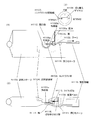
図9は、本発明の実施形態に関わる試料ホルダーの概略構成図である。この試料ホルダーH2は、FIB装置とSTEM装置との共用ホルダーであり、試料ホルダーH2は、先端部H201と端部H202とで構成され、試料ホルダーH2の先端部H201は試料ステージH203に、装着材H210と、コントラスト材H221A,H221Bとを備え、試料ホルダーH2の端部H202は、コントラスト材駆動部H230と切り替えダイヤルH204とを備える。 FIG. 9 is a schematic configuration diagram of a sample holder according to the embodiment of the present invention. The sample holder H2 is a shared holder for the FIB apparatus and the STEM apparatus. The sample holder H2 includes a front end H201 and an end H202. The front end H201 of the sample holder H2 is attached to the sample stage H203 and a mounting material. H210 and contrast materials H221A and H221B, and an end H202 of the sample holder H2 includes a contrast material driving unit H230 and a switching dial H204.
次に、試料ホルダーH2の端部H202の切り替えダイヤルH204は、それぞれ図10(1−a,b)、(2−a,b)、(3−a,b)に示すようにFIB、STEM1、STEM2の向きにダイヤルを切り替えると、試料ホルダーの先端部H201を90度ずつ回転させることが出来、切り替えダイヤルH204のそれぞれの向きにおいて、FIB内、STEM内での試料ホルダーの先端部H201の向きとFIB内のイオンビームB1、STEM内の電子線B2の向きとの関係を示している。 Next, the switching dial H204 of the end portion H202 of the sample holder H2 is shown in FIG. 10 (1-a, b), (2-a, b), (3-a, b), FIB, STEM1, When the dial is switched to the direction of the STEM2, the tip end portion H201 of the sample holder can be rotated by 90 degrees, and the orientation of the tip end portion H201 of the sample holder in the FIB and the STEM in each direction of the switching dial H204. The relationship between the direction of the ion beam B1 in the FIB and the direction of the electron beam B2 in the STEM is shown.
次に、図11(1)、(2)、(3−a,b)に示すように、試料ステージH203に備えた上記装着材H210はそれぞれ金属板からなる装着材H211,H212,H213から構成され、装着材H211と試料ステージH203にはコントラスト材H221a,H221bがそれぞれ平行移動できるような空洞H211a,H211bと、コントラスト材H221a,H221bが互いに衝突しあわず、かつ以下図14に示す試料凸部にコントラスト材H221a,H221bが衝突しないような試料凸部程度の厚さの金属板H206とを備えており、装着材H213は試料ステージH203内を平行移動するように備えた金属ばねH214を供して構成される。 Next, as shown in FIGS. 11 (1), (2), and (3-a, b), the mounting material H210 provided in the sample stage H203 is composed of mounting materials H211, H212, and H213 made of metal plates, respectively. Further, the mounting material H211 and the sample stage H203 do not collide with each other with the cavities H211a and H211b, which allow the contrast materials H221a and H221b to move in parallel, and the contrast materials H221a and H221b. And a metal plate H206 having a thickness about the sample convex portion so that the contrast materials H221a and H221b do not collide with each other, and the mounting material H213 is provided with a metal spring H214 provided to move in parallel within the sample stage H203. Composed.
次に、図12,図13に示すように、試料ステージH203に備えたコントラスト材H221a,H221bは、2次電子発生効率が高くかつ導電性を示す金属であるWからなる金属板で構成される。また、コントラスト材H221a,H221bには、それぞれ金属ワイヤH222a,H222bが取り付けられ、それぞれの金属ワイヤH222について、その一方が金属ばねH223a,H223bを設けてコントラスト材の駆動方向と逆方向の力を常時加えるために一方をホルダー内部に内蔵、固定された金属板H207に取り付けられ、もう一方が、試料ホルダー端部H202に備えたコントラスト材駆動部H230の減速ギヤH224に取り付けられている。コントラスト材駆動部H230は、試料ホルダー端部H202に減速ギヤH224a,H224bを設けて備えられたマイクロメータH231a,H231bを含んでコントラスト材H221を駆動する機能を備えて構成される。なお、金属ワイヤH222に設けた金属ばねH223は、上記コントラスト材H221a,H221bを駆動する際に、コントラスト材H221a,H221bの移動速度およびその動作範囲を制限する(例えば、動作範囲2mm以内)役割を果たす。なお、コントラスト材H221a,H221bの駆動は、それぞれ、試料ホルダーH2のコントラスト材駆動部H230に備えたマイクロメータH231a,H231bを回転させることにより、金属ワイヤH222を試料ホルダーH2の先端部H201と端部H202とをつなぐ方向に前後させることで、上記試料装着材H211に備えた金属板H206と空洞H211a,H211bに沿ってコントラスト材H221a,H221Bbを平行移動させる。 Next, as shown in FIGS. 12 and 13, the contrast materials H221a and H221b provided in the sample stage H203 are composed of a metal plate made of W, which is a metal having high secondary electron generation efficiency and conductivity. . Further, metal wires H222a and H222b are attached to the contrast materials H221a and H221b, respectively, and one of the metal wires H222 is provided with metal springs H223a and H223b so that a force in the direction opposite to the driving direction of the contrast material is always applied. In order to add, one is attached to a metal plate H207 which is built in and fixed inside the holder, and the other is attached to a reduction gear H224 of a contrast material driving unit H230 provided at the sample holder end H202. The contrast material driving unit H230 includes a micrometer H231a and H231b provided with reduction gears H224a and H224b provided on the sample holder end H202, and has a function of driving the contrast material H221. The metal spring H223 provided on the metal wire H222 serves to limit the moving speed of the contrast materials H221a and H221b and the operating range thereof (for example, within the operating range of 2 mm) when driving the contrast materials H221a and H221b. Fulfill. The contrast materials H221a and H221b are driven by rotating the micrometers H231a and H231b provided in the contrast material driving unit H230 of the sample holder H2, respectively, so that the metal wire H222 is connected to the front end portion H201 and the end portion of the sample holder H2. By moving back and forth in the direction connecting H202, the contrast materials H221a and H221Bb are translated along the metal plate H206 provided in the sample mounting material H211 and the cavities H211a and H211b.
図14に示すように、試料ホルダー端部H202に備えたコントラスト材駆動部H230のマイクロメータH231aを回転すると、上記減速ギヤH224aを介してコントラスト材H221aが、コントラスト材駆動部H230のマイクロメータH231bを回転すると、上記減速ギヤH224bを介してコントラスト材H221bが駆動する。コントラスト材H221a,H221bはいずれも上記動作範囲内で駆動するので、試料ホルダーH2をSTEM装置に挿入した状態で、試料ホルダー端部H202に備えたコントラスト材駆動部H230を介してコントラスト材H221a,H221bを駆動させることが出来る。 As shown in FIG. 14, when the micrometer H231a of the contrast material driving unit H230 provided in the sample holder end H202 is rotated, the contrast material H221a is brought into contact with the micrometer H231b of the contrast material driving unit H230 via the reduction gear H224a. When rotated, the contrast material H221b is driven through the reduction gear H224b. Since both the contrast materials H221a and H221b are driven within the above-described operation range, the contrast materials H221a and H221b are connected via the contrast material driving portion H230 provided in the sample holder end portion H202 with the sample holder H2 inserted into the STEM apparatus. Can be driven.
以上のように、上記試料ホルダーH2は、STEM1とSTEM2の両観察方向で断面SEM観察出来るものであり、以下、試料の形状と試料を試料ホルダーH2に装着する方法とを合わせて説明する。 As described above, the sample holder H2 can be observed by cross-sectional SEM in both the STEM1 and STEM2 observation directions. Hereinafter, the shape of the sample and the method of mounting the sample on the sample holder H2 will be described.
図15は、本発明の実施形態2に関わる試料の一例を示す図であり、凸型試料110は図25に示すようなSi半導体デバイス試料であり、一部が凸型となるように試料面111a,111bをもつ形状かつ任意の寸法にダイシング加工して作製される。
FIG. 15 is a diagram illustrating an example of a sample according to
次に、上記凸型試料110の試料ホルダーH2への装着方法について、図16(1−a,b)、(2−a,b)、(3−a,b)を参照しながら説明する。図16(1−a,b)に示すように、ピンセットPで試料ステージH203の装着材(第2装着材)H213を押して、試料ステージH203上に図16(2−a,b)に示すように試料110を載せる。次に、図16(3−a,b)に示すように、装着材H213に備えた金属ばねH214の弾力を利用して、装着材H213で試料110の底面111cを押し、試料面111a,111bと試料底面111cの3点をそれぞれ装着材H212,H211,H213で支持して試料ホルダーH2に装着される。
Next, a method of mounting the
図16に示すように、上記試料ホルダーH2の装着材H213は、凸型試料110を、常に試料ステージH203に沿って移動させ、かつ試料面111a、111bはそれぞれ常に装着材(第1装着材)H212,H211に接するように移動しているため、凸型試料110を常に任意の寸法で作製し、常に試料ホルダーH2の任意の位置でかつ試料ホルダーH2に対して平行に凸型試料110を装着できるようにするものである。
As shown in FIG. 16, the mounting material H213 of the sample holder H2 always moves the
上記のように試料ホルダーH2に装着された凸型試料110を、図15(2−a,b)に示すように、FIB加工により断面観察領域を実施形態1と同様に約0.1μmの厚さまでに薄膜化する。ここで、上記凸型試料110は、観察面121に対して観察を行うものとして、試料ステージH203と観察面122が対向する向きに試料ホルダーH2に装着されているものとする。
As shown in FIG. 15 (2-a, b), the cross-sectional observation region of the
図17に示すように、観察面121が電子線B2照射方向に対向して試料ホルダーH2に装着されている状態で、切り替えダイヤルH204の向きをSTEM1に合わせてSTEMに挿入される。図10(2−a,b)に示すように、STEM装置に上記試料ホルダーH2を挿入した状態で、試料ホルダー端部のコントラスト材駆動部H230に備えたマイクロメータH231bを回転し、凸型試料110の観察面121と反対側に備えたコントラスト材H221bを、装着材H211の空洞H221bに沿って試料ステージ開口部H205に向かって平行移動する。コントラスト材H221bを試料面122側の周辺部に接した状態で、コントラスト材H221bが図17(2−a,b)に示すような位置に到達するとコントラスト材H221Bの駆動は停止する。コントラスト材H221bが、凸型試料110の観察面121の反対側にある試料面122に近い距離でかつ試料周辺部に接触しているので、この状態でSEM観察を行えば、コントラスト材221bにより、観察面121における2次電子発生効率を向上し、かつチャージング現象を低減させて、観察面121について高解像度のSEM像を得ることが出来る。
As shown in FIG. 17, with the observation surface 121 facing the electron beam B2 irradiation direction and mounted on the sample holder H2, the switching dial H204 is inserted into the STEM with the direction of the STEM1 being aligned. As shown in FIG. 10 (2-a, b), in a state where the sample holder H2 is inserted into the STEM apparatus, the micrometer H231b provided in the contrast material driving unit H230 at the end of the sample holder is rotated, and a convex sample is obtained. The contrast material H221b provided on the side opposite to the observation surface 121 of 110 is translated along the cavity H221b of the mounting material H211 toward the sample stage opening H205. When the contrast material H221b reaches a position as shown in FIG. 17 (2-a, b) with the contrast material H221b in contact with the peripheral portion on the sample surface 122 side, the drive of the contrast material H221B is stopped. Since the contrast material H221b is close to the sample surface 122 on the opposite side of the observation surface 121 of the
次に、上記のように試料110を試料ホルダーH2に装着した状態で、観察面122の詳細な断面SEM観察を行う場合を説明する。図10(3−a,b)に示すように、観察面122に対向して電子線B2が照射されるように切り替えダイヤルH204の向きをSTEM2に合わせてSTEMに挿入される。
Next, a case where detailed cross-sectional SEM observation of the observation surface 122 is performed with the
STEM装置に上記試料ホルダーH2を挿入した図10(3−a,b)の状態で、試料ホルダー端部H202のコントラスト材駆動部H230に備えたマイクロメータH231aを回転し、凸型試料110の観察面122と反対側に備えたコントラスト材H221aを、装着材H211の空洞H211aに沿って試料ステージ開口部H205に向かって平行移動する。コントラスト材H221aを試料面121側の周辺部に接した状態で、コントラスト材H221aが図18に示すような位置に到達するとコントラスト材H221aの駆動は停止する。コントラスト材H221aが凸型試料110の観察面122の反対側にある試料面121に近い距離でかつ試料周辺部に接触して設置されているので、この状態でSEM観察を行えば、コントラスト材221bにより、観察面122における2次電子発生効率を向上し、かつチャージング現象を低減させて、観察面122について高解像度のSEM像を得ることが出来る。なお、コントラスト材駆動部230を駆動しない状態では、内部構造観察としてSTEM観察も行うことが出来る。
In the state of FIG. 10 (3-a, b) in which the sample holder H2 is inserted into the STEM apparatus, the micrometer H231a provided in the contrast material driving unit H230 of the sample holder end H202 is rotated to observe the
以上のように、本実施形態2によれば、本発明の試料ホルダーはFIBとSTEMとの共用可能な試料ホルダーの先端部を180°回転させて2方向での詳細なSEM観察が可能となるように、2次電子発生率向上用のコントラスト材としてWを代表とする2次電子発生効率の高い金属から構成されるコントラスト材を試料の両断面付近に設置できるような機能を備えて構成されているので、観察面と反対側に金属膜を堆積させるなどの追加加工工程を省略し、さらに試料をメッシュに接着する工程を省略して、既存のSTEM装置を用いて、薄片化された観察領域について、任意の観察面の観察方向と反対側にコントラスト材を設置することにより、2次電子発生効率を向上させて任意の観察面についての高解像度のSEM観察を行うことが出来る。半導体デバイスのように、微細構造をもつ試料で観察面の両断面構造が互いに異なる場合には、STEM像では試料内部を全て透過してしまうため上記試料の両観察面についての詳細な断面観察が必要となる場合に有効な電子顕微鏡観察方法である。コントラスト材は、試料の観察領域の周辺部となる試料側壁にしか接触しないため、観察領域を破損することもない。 As described above, according to the second embodiment, the sample holder of the present invention enables detailed SEM observation in two directions by rotating the tip of the sample holder that can be shared by FIB and STEM by 180 °. As described above, a contrast material composed of a metal having a high secondary electron generation efficiency represented by W as a contrast material for improving the secondary electron generation rate is provided with a function that can be installed near both cross sections of the sample. Therefore, additional processing steps such as depositing a metal film on the side opposite to the observation surface are omitted, and further, the step of adhering the sample to the mesh is omitted, and the observation is made into a thin piece using an existing STEM device. Perform high-resolution SEM observation of any observation surface by improving the efficiency of secondary electron generation by installing a contrast material on the opposite side of the observation direction of any observation surface. Can. When both cross-sectional structures of the observation surface are different from each other in a sample having a fine structure, such as a semiconductor device, the entire cross-section of the sample is transmitted in the STEM image, so detailed cross-sectional observation of both the observation surfaces of the sample is possible. It is an effective electron microscope observation method when necessary. Since the contrast material contacts only the sample side wall which is the peripheral part of the sample observation region, the observation region is not damaged.
なお、試料は、コントラスト材との位置精度を保つ目的でメッシュに貼り付けずに用いり、試料そのものを直接ピンセットなどで取り扱う。そのため、ピンセットでの試料の取り扱いを容易にするために凸型試料を用いているが、試料形状は実施形態1のようにL字型試料でもよい。ただし、その場合は装着材H211に備えた空洞H211a,H211bや試料ホルダーH2内の金属板H206の位置は、L字型試料の凸部の寸法に合わせて構成する必要がある。 The sample is used without being attached to the mesh for the purpose of maintaining the positional accuracy with the contrast material, and the sample itself is directly handled with tweezers. Therefore, although a convex sample is used to facilitate handling of the sample with tweezers, the sample shape may be an L-shaped sample as in the first embodiment. In this case, however, the positions of the cavities H211a and H211b provided in the mounting material H211 and the metal plate H206 in the sample holder H2 need to be configured in accordance with the dimensions of the convex portions of the L-shaped sample.
また、FIBにより観察領域を含む薄片化部分を切り出した試料を、半円型で3mmΦの切り欠きメッシュ厚さ(例えば、厚さ50μm)に対して中心に、かつ切り欠きメッシュの切り欠き部分に対して平行に金属蒸着膜などで接着させて作製した、μサンプリング試料についても上記と同様の効果を得ることが出来る。その場合、試料ホルダーH2の試料ステージの装着材H211,H212,H213について、切り欠きメッシュが常時任意の位置に装着できるように構成され、上記試料の切り欠きメッシュの切り欠き部分と半円部分の3点を試料装着材H210で支持して試料ホルダーH2に装着する。この状態で、試料ステージに備えたコントラスト材H221a,H221bを、それぞれ試料の切り欠きメッシュの切り欠き部に沿って、試料ステージから試料ステージ開口部に向かって平行移動させ、コントラスト材が観察面と反対側に設置された状態でSEM観察を行えば、上記と同様の効果として2次電子発生効率が向上し、観察領域について高解像度のSEM観察を行うことが出来る。 In addition, the sample obtained by cutting the sliced portion including the observation region by FIB is centered on a semicircular 3 mmφ cutout mesh thickness (for example, thickness 50 μm) and on the cutout portion of the cutout mesh. On the other hand, the same effect as described above can be obtained for the μ sampling sample produced by bonding with a metal vapor deposition film or the like in parallel. In that case, the notch mesh is configured so that the notch mesh can be always mounted at any position on the sample stage mounting materials H211, H212, H213 of the sample holder H2, and the notch portion and the semicircular portion of the notch mesh of the sample are arranged. The three points are supported by the sample mounting material H210 and mounted on the sample holder H2. In this state, the contrast materials H221a and H221b provided in the sample stage are moved in parallel from the sample stage toward the sample stage opening along the notch portion of the notch mesh of the sample, respectively, and the contrast material becomes the observation surface. If SEM observation is performed in a state of being installed on the opposite side, secondary electron generation efficiency is improved as an effect similar to the above, and high-resolution SEM observation can be performed on the observation region.
さらに、本発明の実施形態1,2において、コントラスト材駆動部に、電気信号による制御部を設ければ、コントラスト材が試料周辺部に接触するとコントラスト材に通電して電気信号を検出し、電気信号を検出するとコントラスト材の駆動が停止する機能を設けることが出来るため、さらにコントラスト材と試料との位置精度が向上することが出来るため、コントラスト材による2次電子発生効率を向上させ、かつ観察領域に電子線を照射して一部帯電した電子をコントラスト材にアースすることにより試料表面のチャージング現象を低減することが出来るため、さらに高解像度のSEM像を得ることが出来る。
Furthermore, in
この発明の第3の実施形態を図19〜図24に基づいて説明する。 A third embodiment of the present invention will be described with reference to FIGS.
本発明の実施形態3では、試料の観察領域について2つの観察面がそれぞれ異なる断面構造をもつ場合に、図2と同様に試料ホルダーの切り替えダイヤルをSTEM1およびSTEM2にそれぞれ合わせて試料ホルダー先端部のみを180°回転させることが出来る既存の試料ホルダーを用いて、両観察面について詳細にSEM観察を行うことが出来る電子顕微鏡装置およびそれを用いた電子顕微鏡観察方法を取り上げて説明する。
In
本発明の実施形態3の場合では、2方向の観察面について、コントラスト材による2次電子発生効率向上効果を得るために、試料観察面とその反対側に設置されるコントラスト材との距離を出来るだけ小さくすることが必要であり、本発明の実施形態1,2で試料の薄片化していない周辺部の膜厚の分だけ離れていた観察面とコントラスト材との距離をさらに小さくしてコントラスト材を観察面の反対側に近づける位置精度を備える必要がある。
In the case of
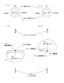
図19は、本発明の実施形態に関わる電子顕微鏡装置の概略構成図である。この電子顕微鏡装置300は、焦点距離が短くかつ高分解能を可能とするための、対物レンズ308による磁界を金属製のポールピース305にかけて構成される磁界型電子レンズを備えたポールピース装着型の電子顕微鏡であり、試料ホルダーH3を挿入する方向と垂直方向に対向して備えた二つのコントラスト材306とコントラスト材駆動部307(ここで、図19では試料ホルダーH3と平行方向に表示されているが、実際には垂直方向に備えられている)と、試料ホルダーH3のx,y方向移動と一方向での傾斜を円滑に行うことの出来るゴニオメータ304と、ポールピース305内で試料の観察面から発生した2次電子を検出する2次電子検出器303とを備えて構成された電子顕微鏡である。ここで、表示は省略しているが、x,y方向はここでは試料ホルダーH3の挿入方向をx方向、コントラスト材306が対向する向きと平行な向きをy方向とするが、逆になっても良い。また、電子顕微鏡300の電子線B2の入射方向と対向する向きをz方向とする。試料ホルダーH3は、既存のFIB装置とSTEM装置との共用ホルダーであり、かつ図1、図2と同様の構成でかつコントラスト材とコントラスト材駆動部とを備えていない試料ホルダーである。
次に、図20(1−a,b)、(2−a,b)は、上記試料ホルダーH3に例えば実施形態1と同様にL字型試料106を切り欠きメッシュ107に貼り付けて作製された試料を図6と同様に試料ホルダーH3に装着した際の、試料ホルダーH3の切り替えダイヤルH106の向きとポールピース内での試料と、駆動していない状態でのコントラスト材306との位置関係を示したものである。切り替えダイヤルH106の向きがSTEM1の向きの場合は、試料ホルダーH3の開口部H112がコントラスト材306aと対向し、切り替えダイヤルH106の向きがSTEM2の向きの場合は、試料ホルダーH3の開口部H112がコントラスト材306bと対向する。
FIG. 19 is a schematic configuration diagram of an electron microscope apparatus according to an embodiment of the present invention. This
Next, FIGS. 20 (1-a, b) and (2-a, b) are produced by attaching the L-shaped
次に、コントラスト材306a,306bは、それぞれ2次電子発生効率が高くかつ導電性を示す金属であるWからなる金属板で構成されており、ある程度高い倍率での観察領域を覆うことが可能な幅でかつFIB加工による局所的に薄片化された領域に収まる程度の任意の大きさ(例えば10μm)であり、それぞれのコントラスト材駆動部307により試料ホルダーH3の挿入方向と垂直方向のみ駆動することが出来る。なお、コントラスト材306を駆動しない状態では、ポールピース内に試料ホルダーH3の先端部を挿入した際にコントラスト材306の先端が当たらない位置にあり、コントラスト材306を駆動するとコントラスト材306の先端部が観察視野中心位置311にあるものとし、コントラスト材306の駆動範囲は、上記の範囲で制限される。また、二つのコントラスト材駆動部307の駆動は、一方が駆動する場合にはもう一方は駆動できないように制限する機能を備えて構成される。
Next, each of the
次に、図23(1)、(2)に示すように、ポールピース305は試料ホルダーH3の先端部の挿入と、ゴニオメータ304による試料ホルダーH3の傾斜と、コントラスト材306a,306bの挿入とが可能な空間をもって構成されている。図23(2)のz方向の高さZ0は電子顕微鏡のフォーカス値が0の時に試料観察面に対して最もSEM像が鮮明に観察出来る高さであり、高さZ1は高さZ0の下でかつ試料観察面を含む薄片化部分に当たらない程度の位置(例えば、高さZ0から2μm下)に位置する高さであり、コントラスト材306a,306bは上面が常に高さZ1の位置で駆動する。
Next, as shown in FIGS. 23 (1) and 23 (2), the
次に、本発明の実施形態3に関わる電子顕微鏡観察方法の一例について、図20〜24を参照しながら詳細に説明する。
本発明に用いる試料は、Si半導体デバイスであり、図25と同様にSi基板103上に半導体デバイスパターン104を形成し、図5(1)に示すように、L字型の形状にダイシング加工したL字型試料106を、3mmΦの半円型の切り欠きメッシュ107に対してL字型試料106の凸部を接着して作製されている。なお、L字型試料106は、観察する部分である凸部と切り欠きメッシュ107が必ず重ならないようにして切り欠きメッシュ107に接着し、電子顕微鏡用試料を作製する。
Next, an example of an electron microscope observation method according to
The sample used in the present invention is a Si semiconductor device, and a
次に、図6に示すように、上記L字型試料106は、試料ステージH103側に切り欠きメッシュ107を、試料ホルダーH3の試料装着材H104側に試料観察面108を配置する向きにして、試料ホルダーH3の試料ステージH103と試料装着材H104とでL字型試料106の切り欠きメッシュ107の一部を挟んで装着される。L字型試料106の観察面108を、図5(2)に示すように、FIB加工により、透過電子顕微鏡でも観察可能な任意の膜厚(例えば、0.1μm)に薄片化する。観察面108、観察面123は、コントラスト材306の幅より十分大きな幅をもって薄片化されているものとする。
Next, as shown in FIG. 6, the L-shaped
次に、L字型試料106は、上記試料の観察面108に対して電子線B2を照射することとし、図20(1−a)に示すように、試料ホルダーH3の端部H102の切り替えダイヤルH106をSTEM1の向きに合わせて、STEMに挿入されている。
Next, the L-shaped
次に、図20(1−b)のコントラスト材306が駆動されていない状態で観察視野中心311に観察面108を移動させて、図23に示すように、上記試料の観察面108のz方向について高さZ0の位置にあわせる。
Next, the observation surface 108 is moved to the observation
次に、図21(2)に示すように、高さZ0の状態で観察面108のx、y方向のみゴニオメータ304でコントラスト材306bを備えた方向に移動させる。この状態で、コントラスト材駆動部307aによりコントラスト材306aを駆動させ、コントラスト材306aの先端を観察視野中心311の位置まで移動させる。このときコントラスト材306aの上面はZ1の高さである。
Next, as shown in FIG. 21 (2), the
次に、コントラスト材306aを上記駆動させたままの状態で、ゴニオメータ304で観察面108をx、y方向のみ移動させて、コントラスト材306aが上記試料の薄片化していない部分に接触せずかつ図23(2)に示すように観察面108の反対側にコントラスト材306aが位置するように移動する。
Next, in a state where the
図23(2)、図24に示すように、コントラスト材306aが観察面108に近接した状態でSEM観察を行えば、薄片化している試料の観察面108は、観察方向と反対側でのコントラスト材306aの設置により、2次電子発生効率が向上し、観察面108について高解像度のSEM観察を行うことが出来る。
As shown in FIGS. 23 (2) and 24, when the SEM observation is performed in a state where the
次に、L字型試料106は、上記試料の観察面123に対して電子線B2を照射することとし、図20(2−a)に示すように、試料ホルダーH3の端部H102の切り替えダイヤルH106をSTEM2の向きに合わせて、STEMに挿入されている。
Next, the L-shaped
次に、図20(2−b)のコントラスト材306が駆動されていない状態で観察視野中心311に観察面123を移動させて、図23に示すように、上記試料の観察面123のz方向について高さZ0の位置にあわせる。
Next, the observation surface 123 is moved to the observation
次に、図22(2)に示すように、高さZ0の状態で観察面123のx、y方向のみゴニオメータ304でコントラスト材306aを備えた方向に移動させる。この状態で、コントラスト材駆動部307bによりコントラスト材306bを駆動させ、コントラスト材306bの先端を観察視野中心311の位置まで移動させる。このときコントラスト材306bの上面はZ1の高さである。
Next, as shown in FIG. 22 (2), only the x and y directions of the observation surface 123 in the state of height Z0 are moved by the
次に、コントラスト材306bを上記駆動させたままの状態で、ゴニオメータ304で観察面123をx、y方向のみ移動させて、コントラスト材306bが上記試料の薄片化していない部分に接触せずかつ図23(2)に示すように観察面123の反対側にコントラスト材306bが位置するように移動する。
Next, with the
図23(2)、図24に示すように、コントラスト材306bが観察面123に近接した状態でSEM観察を行えば、薄片化している試料の観察面123は、観察方向と反対側でのコントラスト材306bの設置により、2次電子発生効率が向上し、観察面123について高解像度のSEM観察を行うことが出来る。
As shown in FIGS. 23 (2) and 24, if the SEM observation is performed in a state where the
以上のように、本発明の実施形態によれば、コントラスト材とそれを駆動する機能を備えた電子顕微鏡を用いれば、観察面と反対側に金属膜を堆積させるなどの追加加工なしに、既存のFIBとSTEMとの共用可能な電子顕微鏡用試料ホルダーを用いて、試料ホルダーの先端部を180°回転させて、任意の観察面について、観察方向と反対側に、試料の薄片化している部分から薄片化していない周辺部までの距離の影響を受けることなく、観察面の反対側に非常に近い距離にコントラスト材を設置する機能を備えているので、任意の観察面について2次電子発生効率を高めて観察面の高解像度のSEM観察を行うことが出来る。半導体デバイスのように、微細構造をもつ試料で観察面の両断面構造が互いに異なる場合には、STEM像では試料内部を全て透過してしまうため上記試料の両観察面についての詳細な断面観察が必要となる場合に有効な電子顕微鏡観察方法である。
また、本発明の実施形態3ではL字型試料を用いたが、観察面を含む薄片化部分がコントラスト材306に当たらない程度の膜厚であれば凸型試料でも良い。
As described above, according to the embodiment of the present invention, when an electron microscope having a contrast material and a function for driving the contrast material is used, the existing film can be formed without additional processing such as depositing a metal film on the side opposite to the observation surface. Using a sample holder for an electron microscope that can be used for both FIB and STEM, the tip of the sample holder is rotated 180 °, and the portion of the sample that is thinned on the opposite side of the observation direction for any observation surface Since it has a function to install a contrast material at a very close distance to the opposite side of the observation surface without being affected by the distance from the surface to the non-flaked periphery, the efficiency of secondary electron generation on any observation surface And high-resolution SEM observation of the observation surface can be performed. When both cross-sectional structures of the observation surface are different from each other in a sample having a fine structure, such as a semiconductor device, the entire cross-section of the sample is transmitted in the STEM image, so detailed cross-sectional observation on both observation surfaces of the sample is possible. It is an effective electron microscope observation method when necessary.
In the third embodiment of the present invention, an L-shaped sample is used. However, a convex sample may be used as long as the thinned portion including the observation surface does not hit the contrast material 306.
なお、本発明の実施形態1,2,3においてSi半導体デバイスを試料として用いているが、試料はSi半導体デバイス以外のものでも良い。 In the first, second, and third embodiments of the present invention, the Si semiconductor device is used as a sample, but the sample may be other than the Si semiconductor device.
本発明にかかる電子顕微鏡装置および走査電子顕微鏡観察方法は、薄片化した試料の観察領域について、試料に追加加工などしてダメージを与えることなく、任意の観察面の2次電子発生効率を向上させて、走査電子顕微鏡観察を高解像度で行うことが出来るため、詳細な構造解析に有用である。 The electron microscope apparatus and the scanning electron microscope observation method according to the present invention improve the efficiency of secondary electron generation on an arbitrary observation surface without damaging the sample by subjecting the observation region of the sliced sample to additional processing. In addition, since scanning electron microscope observation can be performed with high resolution, it is useful for detailed structural analysis.
101 電子顕微鏡用試料
102 観察領域
103 Si基板
104 半導体デバイスパターン
105 電子線
106 L字型試料
107 切り欠きメッシュ
108 観察面
109 試料凸部側壁
110 凸型試料
111 試料面
121 観察面
122 観察面
123 観察面
300 電子顕微鏡装置
301 電子銃
302 コンデンサレンズ
303 2次電子検出器
304 ゴニオメータ
305 ポールピース
306 コントラスト材
307 コントラスト材駆動部
308 対物レンズ
309 投影レンズ
310 透過電子検出器
311 観察視野中心
B2 電子線
H1 試料ホルダー
H101 先端部
H102 端部
H103 試料ステージ
H104 試料装着材
H105 コントラスト材
H106 切り替えダイヤル
H107 コントラスト材駆動部
H108 金属ベルト
H109 プーリ
H110 駆動用軸
H111 押さえローラ
H112 開口部
H113 コイルばね
H114 軸
H115 ばね取り付け部
H2 試料ホルダー
H201 先端部
H202 端部
H203 試料ステージ
H204 切り替えダイヤル
H205 開口部
H206 金属板
H207 金属板
H210 試料装着材
H211 装着材
H211a 空洞
H212 装着材
H213 装着材
H214 金属ばね
H221 コントラスト材
H222 金属ワイヤ
H223 金属ばね
H224 減速ギヤ
H230 コントラスト材駆動部
H231 マイクロメータ
H3 試料ホルダー
Z0 高さ
Z1 高さ
DESCRIPTION OF SYMBOLS 101 Electron microscope sample 102 Observation area 103
Claims (9)
電子線を照射した際に2次電子発生効率が高く導電性を示すタングステンで構成されたコントラスト材と、
前記コントラスト材を駆動するためのコントラスト材駆動部とを備え、
前記試料ホルダーは、集束イオンビーム加工装置と走査透過電子顕微鏡装置に共用可能であり、前記試料ホルダーの先端部に設けた試料ステージに前記試料を装着する装着材と前記コントラスト材を配置し、前記試料ホルダーの基端部に、前記試料ホルダーの先端部の向きを変えるための切り替えダイヤルと前記コントラスト材駆動部とを配置しており、前記コントラスト材は、前記試料における電子線が照射される表面側とは反対の裏面側の所定領域に、前記コントラスト材駆動部を制御することによって配置され、
前記試料ホルダーの試料ステージに、前記試料が位置する開口部と前記コントラスト材の動作範囲を制限する空間とが設けられ、前記コントラスト材の軸端部の一方に、金属ベルトまたは金属ワイヤの一端を巻きつけて固定するプーリが設けられ、前記金属ベルトまたは金属ワイヤの他端は前記試料ステージの駆動用軸に固定され、前記駆動用軸と前記プーリの間には、前記金属ベルトまたは金属ワイヤを押さえる押さえローラが設けられ、前記コントラスト材の軸端部の他方にコイルばねまたは渦巻きばねが設けられていることを特徴とする電子顕微鏡装置。 A sample holder for mounting a sample for scanning electron microscope observation or scanning transmission electron microscope observation;
A contrast material composed of tungsten having high secondary electron generation efficiency and conductivity when irradiated with an electron beam;
A contrast material driving unit for driving the contrast material,
The sample holder can be shared by a focused ion beam processing apparatus and a scanning transmission electron microscope apparatus, and a mounting material for mounting the sample and a contrast material are disposed on a sample stage provided at a tip portion of the sample holder, A switching dial for changing the orientation of the tip of the sample holder and the contrast material driving unit are arranged at the base end of the sample holder, and the contrast material is a surface irradiated with an electron beam in the sample Arranged in a predetermined region on the back side opposite to the side by controlling the contrast material driving unit,
The sample stage of the sample holder is provided with an opening where the sample is located and a space that limits the operating range of the contrast material, and one end of a metal belt or metal wire is attached to one of the shaft end portions of the contrast material. A pulley for winding and fixing is provided, and the other end of the metal belt or metal wire is fixed to a drive shaft of the sample stage, and the metal belt or metal wire is interposed between the drive shaft and the pulley. An electron microscope apparatus characterized in that a pressing roller for pressing is provided, and a coil spring or a spiral spring is provided on the other end of the shaft end of the contrast material.
電子線を照射した際に2次電子発生効率が高く導電性を示すタングステンで構成されたコントラスト材と、
前記コントラスト材を駆動するためのコントラスト材駆動部とを備え、
前記試料ホルダーは、集束イオンビーム加工装置と走査透過電子顕微鏡装置に共用可能であり、前記試料ホルダーの先端部に設けた試料ステージに前記試料を装着する装着材と前記コントラスト材を配置し、前記試料ホルダーの基端部に、前記試料ホルダーの先端部の向きを変えるための切り替えダイヤルと前記コントラスト材駆動部とを配置しており、
前記コントラスト材は、前記試料における電子線が照射される表面側とは反対の裏面側の所定領域に、前記コントラスト材駆動部を制御することによって配置され、
前記試料として、メッシュに張り合わせた透過電子顕微鏡用試料を用い、前記試料ホルダーは、前記試料のメッシュ側を前記試料ステージに載せて前記メッシュを前記装着材と試料ステージとで挟んで装着するように構成され、前記試料が前記電子線と対向するように前記試料ホルダーを電子顕微鏡に挿入することによって、前記試料における前記電子線が照射される表面側とは反対の裏面側において前記コントラスト材が配置されるように駆動することを特徴とする電子顕微鏡装置。 A sample holder for mounting a sample for scanning electron microscope observation or scanning transmission electron microscope observation;
A contrast material composed of tungsten having high secondary electron generation efficiency and conductivity when irradiated with an electron beam;
A contrast material driving unit for driving the contrast material,
The sample holder can be shared by a focused ion beam processing apparatus and a scanning transmission electron microscope apparatus, and a mounting material for mounting the sample and a contrast material are disposed on a sample stage provided at a tip portion of the sample holder, At the base end of the sample holder, a switching dial for changing the direction of the tip of the sample holder and the contrast material driving unit are arranged,
The contrast material is arranged by controlling the contrast material driving unit in a predetermined region on the back surface side opposite to the front surface side irradiated with the electron beam in the sample,
A sample for a transmission electron microscope bonded to a mesh is used as the sample, and the sample holder is mounted by placing the mesh side of the sample on the sample stage and sandwiching the mesh between the mounting material and the sample stage. The contrast material is arranged on the back surface side of the sample opposite to the front surface side irradiated with the electron beam by inserting the sample holder into the electron microscope so that the sample faces the electron beam. The electron microscope apparatus is driven as described above.
電子線を照射した際に2次電子発生効率が高く導電性を示すタングステンで構成されたコントラスト材と、
前記コントラスト材を駆動するためのコントラスト材駆動部とを備え、
前記試料ホルダーは、集束イオンビーム加工装置と走査透過電子顕微鏡装置に共用可能であり、前記試料ホルダーの先端部に設けた試料ステージに前記試料を装着する装着材と前記コントラスト材を配置し、前記試料ホルダーの基端部に、前記試料ホルダーの先端部の向きを変えるための切り替えダイヤルと前記コントラスト材駆動部とを配置しており、
前記コントラスト材は、前記試料における電子線が照射される表面側とは反対の裏面側の所定領域に、前記コントラスト材駆動部を制御することによって配置され、
前記試料ホルダーは、前記試料ステージに試料を任意の位置に装着するための装着材と二つのコントラスト材を配置して構成されており、
前記試料ホルダーの試料ステージに備えた装着材は、金属材から形成され、平坦な試料ステージ上に間隔をあけて互いに対向して試料ステージ開口部の中央側へ一段突き出た当接面が形成された二つの第1装着材と、一端が前記試料ステージに固定された金属ばねを有しかつ平坦な金属材からなる第2装着材とが互いに向かい合って配置され、前記金属ばねにより前記第2装着材が試料挿入方向に伸縮運動することを特徴とする電子顕微鏡装置。 A sample holder for mounting a sample for scanning electron microscope observation or scanning transmission electron microscope observation;
A contrast material composed of tungsten having high secondary electron generation efficiency and conductivity when irradiated with an electron beam;
A contrast material driving unit for driving the contrast material,
The sample holder can be shared by a focused ion beam processing apparatus and a scanning transmission electron microscope apparatus, and a mounting material for mounting the sample and a contrast material are disposed on a sample stage provided at a tip portion of the sample holder, At the base end of the sample holder, a switching dial for changing the direction of the tip of the sample holder and the contrast material driving unit are arranged,
The contrast material is arranged by controlling the contrast material driving unit in a predetermined region on the back surface side opposite to the front surface side irradiated with the electron beam in the sample,
The sample holder is configured by arranging a mounting material and two contrast materials for mounting a sample on an arbitrary position on the sample stage,
The mounting material provided for the sample stage of the sample holder is formed of a metal material, and a contact surface is formed on the flat sample stage so as to be opposed to each other at an interval and projecting one step toward the center side of the sample stage opening. Two first mounting members and a second mounting member made of a flat metal material and having a metal spring fixed at one end to the sample stage, are arranged to face each other, and the second mounting member is arranged by the metal spring. An electron microscope apparatus characterized in that the material is expanded and contracted in the sample insertion direction.
電子線を照射した際に2次電子発生効率が高く導電性を示すタングステンで構成されたコントラスト材と、
前記コントラスト材を駆動するためのコントラスト材駆動部とを備え、
前記試料ホルダーは、集束イオンビーム加工装置と走査透過電子顕微鏡装置に共用可能であり、前記試料ホルダーの先端部に設けた試料ステージに前記試料を装着する装着材と前記コントラスト材を配置し、前記試料ホルダーの基端部に、前記試料ホルダーの先端部の向きを変えるための切り替えダイヤルと前記コントラスト材駆動部とを配置しており、
前記コントラスト材は、前記試料における電子線が照射される表面側とは反対の裏面側の所定領域に、前記コントラスト材駆動部を制御することによって配置され、
前記試料ホルダーは、前記試料ステージに試料を任意の位置に装着するための装着材と二つのコントラスト材を配置して構成されており、
前記試料ホルダーの二つのコントラスト材は、常時コントラスト材の駆動方向と逆方向に力を加えるために、前記試料ステージ内部の固定された部位に取り付けられた金属ばねと、減速ギヤとマイクロメータとを有する前記コントラスト材駆動部に取り付けられた金属ワイヤとをそれぞれ備え、前記コントラスト材駆動部のマイクロメータを回転させ、減速ギヤと金属ワイヤを介して前記コントラスト材を駆動させることを特徴とする電子顕微鏡装置。 A sample holder for mounting a sample for scanning electron microscope observation or scanning transmission electron microscope observation;
A contrast material composed of tungsten having high secondary electron generation efficiency and conductivity when irradiated with an electron beam;
A contrast material driving unit for driving the contrast material,
The sample holder can be shared by a focused ion beam processing apparatus and a scanning transmission electron microscope apparatus, and a mounting material for mounting the sample and a contrast material are disposed on a sample stage provided at a tip portion of the sample holder, At the base end of the sample holder, a switching dial for changing the direction of the tip of the sample holder and the contrast material driving unit are arranged,
The contrast material is arranged by controlling the contrast material driving unit in a predetermined region on the back surface side opposite to the front surface side irradiated with the electron beam in the sample,
The sample holder is configured by arranging a mounting material and two contrast materials for mounting a sample on an arbitrary position on the sample stage,
The two contrast members of the sample holder always have a metal spring, a reduction gear and a micrometer attached to a fixed part inside the sample stage in order to apply a force in the direction opposite to the driving direction of the contrast material. An electron microscope comprising: a metal wire attached to the contrast material driving unit, wherein the contrast material driving unit is rotated by a micrometer to drive the contrast material via a reduction gear and the metal wire. apparatus.
電子線を照射した際に2次電子発生効率が高く導電性を示すタングステンで構成されたコントラスト材と、
前記コントラスト材を駆動するためのコントラスト材駆動部とを備え、
前記試料ホルダーは、集束イオンビーム加工装置と走査透過電子顕微鏡装置に共用可能であり、前記試料ホルダーの先端部に設けた試料ステージに前記試料を装着する装着材と前記コントラスト材を配置し、前記試料ホルダーの基端部に、前記試料ホルダーの先端部の向きを変えるための切り替えダイヤルと前記コントラスト材駆動部とを配置しており、
前記コントラスト材は、前記試料における電子線が照射される表面側とは反対の裏面側の所定領域に、前記コントラスト材駆動部を制御することによって配置され、
前記試料ホルダーは、前記試料ステージに試料を任意の位置に装着するための装着材と二つのコントラスト材を配置して構成されており、
前記試料ホルダーに用いる電子顕微鏡用試料は、観察領域を含む部分が凸型に突出した凸部となり、前記凸部の外周部は一様に所定の高さになっており、
前記第2装着材が前記試料の底面に当接し、互いに対向した二つの第1装着材に形成された当接面が前記試料の凸部外周部の試料面に当接して、これらの当接面が位置決めストッパーとしての役割を果たしながら、前記試料の凸部外周部の試料面と、前記試料の底面とを挟んで前記試料を常時任意の位置に装着可能としたことを特徴とする電子顕微鏡装置。 A sample holder for mounting a sample for scanning electron microscope observation or scanning transmission electron microscope observation;
A contrast material composed of tungsten having high secondary electron generation efficiency and conductivity when irradiated with an electron beam;
A contrast material driving unit for driving the contrast material,
The sample holder can be shared by a focused ion beam processing apparatus and a scanning transmission electron microscope apparatus, and a mounting material for mounting the sample and a contrast material are disposed on a sample stage provided at a tip portion of the sample holder, At the base end of the sample holder, a switching dial for changing the direction of the tip of the sample holder and the contrast material driving unit are arranged,
The contrast material is arranged by controlling the contrast material driving unit in a predetermined region on the back surface side opposite to the front surface side irradiated with the electron beam in the sample,
The sample holder is configured by arranging a mounting material and two contrast materials for mounting a sample on an arbitrary position on the sample stage,
The sample for the electron microscope used for the sample holder is a convex portion in which the portion including the observation region protrudes in a convex shape, and the outer peripheral portion of the convex portion is uniformly at a predetermined height,
The second mounting material is in contact with the bottom surface of the sample, and the contact surfaces formed on the two first mounting materials facing each other are in contact with the sample surface of the outer peripheral portion of the convex portion of the sample. An electron microscope characterized in that the sample can always be mounted at an arbitrary position with the surface serving as a positioning stopper between the sample surface of the outer peripheral portion of the convex portion of the sample and the bottom surface of the sample apparatus.
前記走査透過電子顕微鏡観察を行うための試料を装着する試料ホルダーと、
電子線を照射した際に2次電子発生効率が高く導電性を示すタングステンで構成された二つのコントラスト材と、
前記コントラスト材を駆動するための二つのコントラスト材駆動部とを備え、
前記コントラスト材は、前記試料における電子線が照射される表面側とは反対の裏面側の所定領域に、前記コントラスト材駆動部を制御することによって配置され、
前記二つのコントラスト材は、前記電子顕微鏡試料の薄片化していない周辺部の試料膜厚の影響を受けないために前記試料の薄片領域よりも小さい幅で、かつ薄片化されてない試料周辺部を損傷しない大きさの金属板で構成され、観察面の反対側の面から所定の距離をもつ高さに前記コントラスト材が設置されることを特徴とする電子顕微鏡装置。 An electron microscope apparatus equipped with a pole piece-mounted scanning transmission electron microscope,
A sample holder for mounting a sample for performing the scanning transmission electron microscope observation;
Two contrast materials composed of tungsten having high secondary electron generation efficiency and conductivity when irradiated with an electron beam;
Two contrast material driving units for driving the contrast material,
The contrast material is arranged by controlling the contrast material driving unit in a predetermined region on the back surface side opposite to the front surface side irradiated with the electron beam in the sample,
Since the two contrast materials are not affected by the sample film thickness of the non-flaked peripheral portion of the electron microscope sample, the width of the sample is smaller than that of the thin piece region of the sample, and the non-flaked sample peripheral portion is An electron microscope apparatus comprising a metal plate having a size that is not damaged, wherein the contrast material is installed at a height having a predetermined distance from a surface opposite to the observation surface.
前記走査透過電子顕微鏡観察を行うための試料を装着する試料ホルダーと、
電子線を照射した際に2次電子発生効率が高く導電性を示すタングステンで構成された二つのコントラスト材と、
前記コントラスト材を駆動するための二つのコントラスト材駆動部とを備え、
前記コントラスト材は、前記試料における電子線が照射される表面側とは反対の裏面側の所定領域に、前記コントラスト材駆動部を制御することによって配置され、
前記電子顕微鏡のポールピース内部に備えた前記試料ホルダー先端部が移動できる空間内で、前記二つのコントラスト材は前記試料ホルダーに装着した試料観察面の観察方向と反対側の任意の高さに配置され、前記任意の高さで電子線の入射方向に対して垂直方向にのみ駆動する機能を備えていることを特徴とする電子顕微鏡装置。 An electron microscope apparatus equipped with a pole piece-mounted scanning transmission electron microscope,
A sample holder for mounting a sample for performing the scanning transmission electron microscope observation;
Two contrast materials composed of tungsten having high secondary electron generation efficiency and conductivity when irradiated with an electron beam;
Two contrast material driving units for driving the contrast material,
The contrast material is arranged by controlling the contrast material driving unit in a predetermined region on the back surface side opposite to the front surface side irradiated with the electron beam in the sample,
In the space where the tip of the sample holder provided inside the pole piece of the electron microscope can move, the two contrast materials are arranged at an arbitrary height opposite to the observation direction of the sample observation surface mounted on the sample holder. An electron microscope apparatus having a function of driving only in a direction perpendicular to the incident direction of the electron beam at the arbitrary height.
Priority Applications (1)
| Application Number | Priority Date | Filing Date | Title |
|---|---|---|---|
| JP2004036328A JP4012158B2 (en) | 2004-02-13 | 2004-02-13 | Electron microscope apparatus and electron microscope observation method |
Applications Claiming Priority (1)
| Application Number | Priority Date | Filing Date | Title |
|---|---|---|---|
| JP2004036328A JP4012158B2 (en) | 2004-02-13 | 2004-02-13 | Electron microscope apparatus and electron microscope observation method |
Publications (3)
| Publication Number | Publication Date |
|---|---|
| JP2005228608A JP2005228608A (en) | 2005-08-25 |
| JP2005228608A5 JP2005228608A5 (en) | 2006-07-20 |
| JP4012158B2 true JP4012158B2 (en) | 2007-11-21 |
Family
ID=35003137
Family Applications (1)
| Application Number | Title | Priority Date | Filing Date |
|---|---|---|---|
| JP2004036328A Expired - Fee Related JP4012158B2 (en) | 2004-02-13 | 2004-02-13 | Electron microscope apparatus and electron microscope observation method |
Country Status (1)
| Country | Link |
|---|---|
| JP (1) | JP4012158B2 (en) |
Family Cites Families (10)
| Publication number | Priority date | Publication date | Assignee | Title |
|---|---|---|---|---|
| JPH06139986A (en) * | 1992-10-23 | 1994-05-20 | Hitachi Ltd | Two-axial tilting sample holder for electron microscope |
| JP3184675B2 (en) * | 1993-09-22 | 2001-07-09 | 株式会社東芝 | Measuring device for fine patterns |
| JPH0887972A (en) * | 1994-09-20 | 1996-04-02 | Hitachi Ltd | Sample holder |
| JP3429886B2 (en) * | 1995-02-08 | 2003-07-28 | 株式会社日立製作所 | Sample holder |
| JP3469054B2 (en) * | 1997-08-08 | 2003-11-25 | 東芝マイクロエレクトロニクス株式会社 | Sample processing holder system |
| JP3805547B2 (en) * | 1999-01-21 | 2006-08-02 | 株式会社日立製作所 | Sample preparation equipment |
| JP2001015056A (en) * | 1999-04-28 | 2001-01-19 | Canon Inc | Sample holder and spacer for use therein |
| JP2001183317A (en) * | 1999-12-24 | 2001-07-06 | Nec Corp | Sample holder for secondary ion mass spectroscope and method for regulating its position |
| JP2003100245A (en) * | 2001-09-25 | 2003-04-04 | Hitachi Ltd | Sample holder for focused ion beam machining observation device |
| JP2003263969A (en) * | 2002-03-08 | 2003-09-19 | Jeol Ltd | Sample holder |
-
2004
- 2004-02-13 JP JP2004036328A patent/JP4012158B2/en not_active Expired - Fee Related
Also Published As
| Publication number | Publication date |
|---|---|
| JP2005228608A (en) | 2005-08-25 |
Similar Documents
| Publication | Publication Date | Title |
|---|---|---|
| US5907157A (en) | Method and apparatus for preparing specimen | |
| US5270552A (en) | Method for separating specimen and method for analyzing the specimen separated by the specimen separating method | |
| EP2413126B1 (en) | TEM-lamella and process for its manufacture | |
| US8487270B2 (en) | Particle beam device and method for use in a particle beam device | |
| US7777185B2 (en) | Method and apparatus for a high-resolution three dimensional confocal scanning transmission electron microscope | |
| KR102195030B1 (en) | Ion milling device and ion milling method | |
| EP2704178B1 (en) | Imaging a sample in a TEM equipped with a phase plate | |
| EP2811288B1 (en) | Method for electron tomography | |
| US10483084B2 (en) | Object preparation device and particle beam device having an object preparation device and method for operating the particle beam device | |
| JP2010003617A (en) | Sample stand, sample rotating holder, construction method of sample stand, and sample stand construction method, and test piece analyzing method | |
| US20200035444A1 (en) | Device and method for preparing microscopic samples | |
| US20160139398A1 (en) | Specimen Holder, Specimen Preparation Device, and Positioning Method | |
| JP2004245660A (en) | Manufacture of chip sample, and method and system for observing wall surface of the same | |
| JP2007188905A (en) | Sample holder for charged particle beam device | |
| JP2009216534A (en) | Thin-film sample preparation method | |
| JP2006309952A (en) | Composite charged particle beam device and method for determining irradiation position in it | |
| WO2011163397A1 (en) | Microfabricated high-bandpass foucault aperture for electron microscopy | |
| JP4012158B2 (en) | Electron microscope apparatus and electron microscope observation method | |
| US10319561B2 (en) | Object preparation device and particle beam device with an object preparation device and method for operating the particle beam device | |
| US9012841B2 (en) | Specimen holder for observing cross section of specimen and method for controlling the same | |
| EP1557867A1 (en) | Focussing lens for charged particle beams | |
| JP2011222426A (en) | Composite charged particle beam device | |
| WO2015185805A1 (en) | Slide holder for an optical microscope | |
| CN108593690B (en) | Sample surface structure imaging method based on transmission electron microscope | |
| CN111081515B (en) | Charged particle beam device and sample processing and observing method |
Legal Events
| Date | Code | Title | Description |
|---|---|---|---|
| A521 | Request for written amendment filed |
Free format text: JAPANESE INTERMEDIATE CODE: A523 Effective date: 20060602 |
|
| RD04 | Notification of resignation of power of attorney |
Free format text: JAPANESE INTERMEDIATE CODE: A7424 Effective date: 20060605 |
|
| A131 | Notification of reasons for refusal |
Free format text: JAPANESE INTERMEDIATE CODE: A131 Effective date: 20060704 |
|
| A521 | Request for written amendment filed |
Free format text: JAPANESE INTERMEDIATE CODE: A523 Effective date: 20060830 |
|
| A131 | Notification of reasons for refusal |
Free format text: JAPANESE INTERMEDIATE CODE: A131 Effective date: 20061031 |
|
| A131 | Notification of reasons for refusal |
Free format text: JAPANESE INTERMEDIATE CODE: A131 Effective date: 20070403 |
|
| A521 | Request for written amendment filed |
Free format text: JAPANESE INTERMEDIATE CODE: A523 Effective date: 20070601 |
|
| TRDD | Decision of grant or rejection written | ||
| A01 | Written decision to grant a patent or to grant a registration (utility model) |
Free format text: JAPANESE INTERMEDIATE CODE: A01 Effective date: 20070815 |
|
| A61 | First payment of annual fees (during grant procedure) |
Free format text: JAPANESE INTERMEDIATE CODE: A61 Effective date: 20070906 |
|
| FPAY | Renewal fee payment (event date is renewal date of database) |
Free format text: PAYMENT UNTIL: 20100914 Year of fee payment: 3 |
|
| FPAY | Renewal fee payment (event date is renewal date of database) |
Free format text: PAYMENT UNTIL: 20110914 Year of fee payment: 4 |
|
| FPAY | Renewal fee payment (event date is renewal date of database) |
Free format text: PAYMENT UNTIL: 20120914 Year of fee payment: 5 |
|
| LAPS | Cancellation because of no payment of annual fees |