JP4010744B2 - Video signal sample pulse generator for electronic endoscope - Google Patents
Video signal sample pulse generator for electronic endoscope Download PDFInfo
- Publication number
- JP4010744B2 JP4010744B2 JP2000165563A JP2000165563A JP4010744B2 JP 4010744 B2 JP4010744 B2 JP 4010744B2 JP 2000165563 A JP2000165563 A JP 2000165563A JP 2000165563 A JP2000165563 A JP 2000165563A JP 4010744 B2 JP4010744 B2 JP 4010744B2
- Authority
- JP
- Japan
- Prior art keywords
- pulse
- output
- switch
- signal
- setting
- Prior art date
- Legal status (The legal status is an assumption and is not a legal conclusion. Google has not performed a legal analysis and makes no representation as to the accuracy of the status listed.)
- Expired - Fee Related
Links
Images


Description
【0001】
【発明の属する技術分野】
本発明は、電子内視鏡に設けられ、映像信号のサンプリングのタイミングを調整する回路に関する。
【0002】
【従来の技術】
近年医療分野では、電子内視鏡(電子スコープ)を用いた診療が広く行われている。電子内視鏡は、映像信号の処理などを行う信号処理装置(プロセッサ)やTVモニタなどの画像表示装置とともに用いられる。電子内視鏡は信号処理装置に装着され、電子内視鏡の先端において撮像された映像は、信号処理装置を介して画像表示装置に伝送され表示される。電子内視鏡の種類は多様であり、目的に応じ様々なものが使用される。しかし、電子内視鏡毎に個別に信号処理装置を設けることは無駄が多いため、信号処理の方法が同じ電子内視鏡では、信号処理装置が共有される。
【0003】
撮像素子(CCD:charge coupled device)は電子内視鏡の挿入部の先端に設けられるが、挿入部の先端は小型であることが望ましい。したがって、CCDの制御信号を出力するCCD駆動回路やCCDからの映像信号をサンプルホールドするための相関二重サンプリング(CDS:correlated double sampling)回路は、電子内視鏡の外部装置である信号処理装置に設けられていた。制御信号がCCD駆動回路から出力され、その制御信号に基づく映像信号がCDS回路に到達するまでの伝搬遅延時間は、電子内視鏡の挿入部の長さに相関する。電子内視鏡の挿入部の長さは、1メートル未満のものから数メートルのものまであるため、このときの伝搬遅延時間は映像信号の処理にとって無視できない大きさとなる。信号処理装置を共有する電子内視鏡であっても、電子内視鏡の挿入部の長さは目的に応じて様々であるため、挿入部の長さが異なるとCCDからの映像信号をCDS回路においてサンプルホールドするタイミングが異なり、適正なサンプリングを行えない。したがって、従来信号処理装置には、長さの異なる電子内視鏡それぞれに対応した遅延線が設けられていた。しかし、長さの異なる多くの電子内視鏡において信号処理装置を共有するには、信号処理装置に多数の遅延線を備える必要があるほか、装着された電子内視鏡に応じて遅延線の切り換えを行う必要があるため、その構成や処理が煩雑になるという問題があった。
【0004】
この問題に対して、特許第2790948号には、相関二重サンプリング回路と相関二重サンプリング回路へ供給するクランプパルス、サンプルパルスの位相を変えることができる回路とを電子内視鏡の操作部または信号処理装置との接続部に設けた電子内視鏡装置が開示されている。特許第2790948号に開示された電子内視鏡装置において、クランプパルスおよびサンプルパルスの位相はポテンショメータ(可変抵抗)を用いたRC回路の時定数を調節することによりアナログ的に調整される。しかし、ポテンショメータを用いる構成は回路の小型化に適さないという問題があるほか、アナログ回路は互いに近接して設ける必要があるので、ポテンショメータ、CCD駆動回路、CDS回路等は一体的に近接して配置される必要がある。また、位相調整が簡便に行なえるためには、ポテンショメータを簡単に操作できる位置に設け、その保護カバー等も容易に着脱できる構成にする必要がある。しかし。このような配置・構成は、頻繁に洗浄される電子内視鏡においては、ポテンショメータ、CCD駆動回路、CDS回路等の防水の点から問題がある。さらに、上述した回路の小型化の困難性、ポテンショメータの配置、カバー等の構成の問題は、電子内視鏡の操作部等の小型化、形状を制限し、操作性が重要である操作部の設計には大きな障害となる。また更に、ポテンショメータを用いた位相調整には、ポテンショメータの摘みを操作する必要があり調節操作は煩雑である。
【0005】
【発明が解決しようとする課題】
本発明は、上記問題に鑑みてなされたものであり、小型であり、回路配置の自由度が高く、位相調整が容易な電子内視鏡の映像信号サンプルパルス生成装置を得ることを目的としている。
【0006】
【課題を解決するための手段】
本発明の電子内視鏡の映像信号サンプルパルス生成装置は、撮像素子と、撮像素子において得られる映像信号をサンプリングするためのサンプリング回路と、撮像素子を駆動するための撮像素子駆動パルスを生成する撮像素子駆動パルス生成手段と、周期的なクロックパルスを発生するクロックと、所定の数の出力端子を備えクロックパルスが発生する毎にそのパルス数を計数し、計数が出力端子の数の範囲で循環的に繰り返し行われ、計数における各計数値と出力端子とが1対1に対応し、計数値に対応する出力端子のみに信号を出力するシフトカウンタと、出力端子の各々に接続されたスイッチからなる第1のスイッチ群と、出力端子の各々に接続されたスイッチからなる第2のスイッチ群と、第1及び第2のスイッチ群の各スイッチのオン・オフ設定を記録する記録媒体と、記録媒体に記憶された設定内容に基づいて第1及び第2のスイッチ群の各スイッチのオン・オフ設定を行うスイッチ設定手段と、記録媒体に記録される各スイッチの設定内容の設定または変更を行うオン・オフ設定記録手段とを備え、撮像素子駆動パルス生成手段が、シフトカウンタの所定の出力端子から出力される信号に基づいて撮像素子駆動パルスを生成し、サンプリング回路のサンプリングを制御する少なくとも2つのサンプルパルスが、スイッチ設定手段によるオン状態に設定された第1及び第2のスイッチ群それぞれからの出力に基づくものであることを特徴としている。
【0007】
例えばサンプリング回路は、相関二重サンプリング回路であり、サンプルパルスがクランプパルス及びサンプルホールドパルスであり、クランプパルス及びサンプルホールドパルスの一方が第1のスイッチ群から出力され、他方が第2のスイッチ群から出力される。また例えば記録媒体は、EEPROMである。
【0008】
オン・オフ設定記録手段は好ましくは、電子内視鏡の外部に設けられたコンピュータからの信号に基づいて駆動される。これにより、オン・オフ設定記録手段のためのスペースを節約することができる。
【0009】
例えば、撮像素子駆動パルスは、出力端子の1つから出力される信号、または複数の出力端子から出力される信号の論理和であり、撮像素子駆動パルスが複数の出力端子から出力される信号の論理和であるとき、出力端子は計数の循環において連続する計数値に対応する。また、例えば撮像素子はCCD撮像素子であり、撮像素子駆動パルスの1つはCCD水平レジスタ転送クロックであり、CCD水平レジスタ転送クロックは、出力端子の数の半分の数の出力端子から出力される信号の論理和であり、これらの出力端子は計数の循環において連続する計数値に対応する。
【0010】
【発明の実施の形態】
以下、本発明の実施の形態を図面を参照して説明する。
図1は本発明の実施形態である電子内視鏡を備えた電子内視鏡システムの構成を概略的に示すブロック図である。
【0011】
電子内視鏡10は、信号処理装置13に着脱自在に接続されており、信号処理装置13はTVモニタ15に接続されている。電子内視鏡10の操作部にはCCD駆動制御回路11が設けられ、挿入部の先端にはCCD(撮像素子)12が設けられている。また、信号処理装置13には、プロセス処理回路14が設けられている。CCD12は、CCD駆動制御回路11から出力されるCCD駆動パルス(CCD水平レジスタ転送クロック、リセットゲートクロック等)に基づいて動作し、例えば、従来公知の面順次撮像方式により映像の検出が行われる。CCD12で検出された信号は、CCD駆動制御回路11内のCDS回路(図2参照)においてサンプリングされ、信号処理装置13のプロセス処理回路14へ映像信号VS1として送られる。
【0012】
プロセス処理回路14では電子内視鏡10から出力された映像信号VS1の処理が行われる。すなわち映像信号VS1は、適度に増幅された後、映像帯域のフィルタリング処理、S/H処理、増幅処理、クランプ処理、クリップ処理、ガンマ処理等の前段信号処理が施され、デジタルの画像信号に変換される。デジタルの画像信号はRGB毎に一時的に画像メモリ(図示せず)に記憶され、RGBの画像信号が1組揃うと再びアナログ信号に変換されて後段信号処理が行われる。後段信号処理では、フィルタリング処理、増幅処理、ガンマ処理、クランプ処理、クリップ処理、エンハンス処理、レベル調整等が行われ、例えばコンポジット映像信号など、規格化されたテレビジョン信号(TV信号)に変換されTVモニタ15へ出力される。
【0013】
電子内視鏡10と信号処理装置13との間では、映像信号VS1のほかに信号CS1、CS2の送受信が行われる。信号CS1は、プロセス処理回路14から電子内視鏡10に出力される信号であり、CCDの駆動タイミングやカラーバランスの設定を行うためのデータなどである。一方、信号CS2は、CCD駆動制御回路11から信号処理装置13へ出力される信号であり、例えば、電子内視鏡の種類や電子内視鏡が信号処理装置13へ装着されたか否かを知らせるための装着信号などである。
【0014】
また、工場出荷時やメンテナンスを行うときなど、CCD駆動パルスとCDS制御パルス(クランプパルス、サンプルホールドパルス)の出力タイミング、すなわち、CCD駆動パルスとCDS制御パルスとの相対的な位相を調整する際には、コンピュータ16が電子内視鏡10のCCD駆動制御回路11に接続される。このとき、電子内視鏡の伝搬遅延時間は、例えばCCD駆動パルスが出力されるCCD駆動制御回路11の出力端子aと検出された映像信号を入力するための入力端子bに、オシロスコープ(図示せず)を接続し、端子a、bにおいて検出される信号波形から算出される。オペレータは、オシロスコープを用いて算出された伝搬遅延時間をキーボード17から入力することにより、CCD駆動パルスとCDS制御パルスの位相を調整することができる。
【0015】
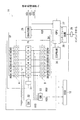
次に図2を参照して本実施形態のCCD駆動制御回路11について説明する。図2は、図1におけるCCD駆動制御回路11の概略的な回路構成を示したブロック図である。
【0016】
CCD駆動制御回路11は、シフトカウンタ20、OR回路22、23、スイッチ群A、B、CDS回路26、CPU27、インターフェース回路28、EEPROM(electrically erasable programmable read only memory)30、及びクロック31から構成される。
【0017】
CCD12において検出された映像信号VS0は、CDS回路26においてサンプルホールドされ、映像信号VS1として信号処理装置13(図1参照)に出力される。CDS回路26は、CDS制御パルスであるクランプパルスCP及びサンプルホールドパルスSHにより制御される。クランプパルスCPは、10個のスイッチA0〜A9からなるスイッチ群Aの中の1つのスイッチから出力され、サンプルホールドパルスSHは、10個のスイッチB0〜B9からなるスイッチ群Bの中の1つのスイッチから出力される。
【0018】
スイッチ群A、Bの各スイッチA0〜A9、B0〜B9は、それぞれシフトカウンタ20に接続されている。シフトカウンタ20に付された0〜9までの番号は、シフトカウンタ20において計数されるカウント値に対応しており、シフトカウンタ20の機能を模式的に表わしている。シフトカウンタ20は、クロック31から出力される規則的なパルス信号(クロックパルス)の数を0から9までカウントし、現在のカウント値に対応する端子にパルス信号を出力する。カウント値が9に達するとまた0からのカウントを開始し、この循環的計数動作を繰り返す。
【0019】
スイッチA0〜A9及びスイッチB0〜B9は、それぞれシフトカウンタ20のカウント値0〜9に対応する端子に接続されている。したがって、シフトカウンタ20は、現在のカウント値に対応するスイッチにパルス信号を出力する。例えば、現在シフトカウンタ20においてカウント値が0であれば、カウント値0に対応するスイッチA0及びスイッチB0にパルス信号が出力される。その後カウント値が1に変わると、カウント値1に対応するスイッチA1及びスイッチB1にパルス信号が出力され、スイッチA0とスイッチB0に対するパルス信号の出力は終了する。以下同様にスイッチ群A、BのスイッチA2、B2〜スイッチA9、B9に順次対毎にパルス信号が出力され、このパルス信号の出力動作は循環的に繰り返される。
【0020】
クランプパルスCPは、スイッチ群Aの中でオン状態に設定されたスイッチを介してシフトカウンタ20から出力される。また、サンプルホールドパルスSHは、スイッチ群Bの中でオン状態に設定されたスイッチを介してシフトカウンタ20から出力される。スイッチ群A及びスイッチ群Bにおけるスイッチのオン・オフの設定は、EEPROM30に記録されたデータに基づいてCPU27により行われる。前述したように、このデータは電子内視鏡10にコンピュータ16(図1参照)を接続することにより、キーボード17を用いてオペレータが設定することができる。すなわち、CPU27は、コネクタ29に接続されるインターフェースケーブルによりコンピュータ16と接続でき、インターフェース回路28を介してコンピュータ16と通信できる。CPU27はコンピュータ16からの指令に従ってEEPROM30の内容を設定・変更することができる。
【0021】
OR回路22は、シフトカウンタ20のカウント値0〜4に対応する4つの端子に接続されており、これらの端子から出力されるパルス信号に対して論理和をとり、CCDにおける水平転送の駆動を制御する水平レジスタ転送クロックH10としてCCD12へ出力する。すなわち、水平レジスタ転送クロックH10は、シフトカウンタ20のカウント値が0〜4の期間はハイレベルで、カウント値が5〜9の期間はローレベルの周期的なパルス信号となる。また、OR回路23は、シフトカウンタ20のカウント値が5〜9に対応する4つの端子に接続されており、これらの端子から出力されるパルス信号に対して論理和をとり、水平レジスタ転送クロックH20としてCCD12へ出力する。すなわち、水平レジスタ転送クロックH20は、水平レジスタ転送クロックH10の反転パルスであり、シフトカウンタ20のカウント値が0〜4の期間はローレベルで、カウント値が5〜9の期間はハイレベルの周期的なパルス信号である。また、シフトカウンタ20のカウント値0に対応する端子は、CCD12のリセットゲートクロックを入力するため端子に接続されており、カウント値0のときシフトカウンタ20から出力されるパルス信号は、リセットゲートクロックRG0としてCCD12へ出力される。
【0022】
なお、クロック31はCPU27に接続されており、CPU27からの信号指令に基づいて制御される。また、CPU27と信号処理装置13のプロセス処理回路14(図1参照)とはコネクタ(図示せず)を介して接続されており、信号CS1と信号CS2の送受信が行なわれる。
【0023】
次に図2、図3、図4を参照して本実施形態においてCCD駆動パルス及びCDS制御パルスを出力するためのパルス信号出力動作について説明する。
【0024】
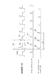
図3(a) 、(b)は、OR回路22、23から出力されるCCD水平レジスタ転送クロックH10、H20をそれぞれ示しており、図3(c)は、リセットゲートクロックRG0が出力されるタイミングを示している。また、図3(d)は、上記CCD水平レジスタ転送クロックH10、H20、及びリセットゲートクロックRG0が遅延無くCCDへ入力されたときにCCDから出力される映像信号VSを示している。期間Trは、リセットゲートクロックRG0のパルス幅に対応するリセット期間であり、期間Tfはリセット期間に確定したリセット雑音のみが出力されるフィードスルー期間である。また、期間Tsはリセット雑音とCCDの各画素で検出される画像(映像)信号が重畳して出力される映像信号出力期間である。
【0025】
シフトカウンタ20の繰り返し周期(0から9までカウントする期間)は、水平レジスタ転送クロックH10、H20の周期、すなわち映像信号のピクセルクロック期間Tp(例えば、69.8ns)に相当する。したがって、シフトカウンタ20の1カウントはTp/10であり、カウント値が0の期間出力されるリセットゲートクロックRG0のパルス幅(リセット期間Tr)は、Tp/10となる。
【0026】
図3(e)は、電子内視鏡挿入部における伝搬遅延時間を考慮したときのCDS回路26に入力される映像信号VS0を示しており、図3(d)に示された遅延を考慮しない映像信号VSよりも伝搬遅延時間Td分遅れている。すなわち、図3(e)に示された映像信号VS0は、CCD駆動制御回路11から出力されたCCD駆動パルス(図3(a)〜(c)のパルス)がCCD12に到達し、CCD12から出力される映像信号がCSD回路26に達するまでの時間遅延されている。なお、図3(d)に示された1周期分の映像信号S0は、図3(e)に示された1周期分の映像信号S1に対応する。伝搬遅延時間Tdは、挿入部の長さが例えば2m強(信号線は往復で4m強)のとき約14nsである。ピクセルクロック期間Tpが69.8nsであるとすると、14nsはシフトカウンタ20の2カウント(14/69.8×10≒2)の期間に相当する。
【0027】
図4は、図3(d)に示された映像信号VS(遅延がないときの映像信号)とシフトカウンタ20のカウント値との関係を1周期分示したものである。図4において、例えば、シフトカウンタ20のカウント値が4のとき(リセット期間Trの開始からTc期間経過後)に信号をクランプし、カウンタ値が9のとき(リセット期間Trの開始からTs期間経過後)にサンプルホールドするのが、サンプリングのタイミングとして好適である場合、同様のタイミングで図3(e)に示された映像信号VS0(Td時間遅延された映像信号)に対してクランプ及びサンプルホールドを行おうとすれば、クランプパルスCP及びサンプルホールドパルスSHの出力タイミングを伝搬遅延時間Tdだけ遅らせなければならない。上述のように伝搬遅延時間Tdがシフトカウンタ20の2カウント分の期間に対応する場合、各信号の好適な出力タイミングは2カウント分遅れるので、クランプパルスCPの出力タイミングはカウント値が6のとき、サンプルホールドパルスSHの出力タイミングはカウント値が1のとき好適となる。すなわち、スイッチ群AではスイッチA6がオン状態に設定され、スイッチ群BではスイッチSB1がオン状態に設定される。
【0028】
図3(f)、図3(g)には、図3(e)の映像信号VS0に対するクランプパルスCP、及びサンプルホールドパルスSHの出力タイミングが示されている。すなわち、信号S2、S3は、図3(e)の信号S1に対するクランプパルス信号、及びサンプルホールド信号である。ここで、期間t1はTd+Tcであり7カウント分(カウント値0〜6)の期間に対応している。また、期間t2はTd+Tsであり12カウント分(カウント値0〜9及び次の周期の0〜1)の期間に対応している。なお、パルス信号S4は1周期前の映像信号に対するサンプルホールドパルス信号となる。
【0029】
以上の説明は、伝搬遅延時間Tdがピクセルクロック期間Tpよりも短い場合のパルス信号出力動作についてであるが、伝搬遅延時間がピクセルクロック期間Tpよりも長い場合のパルス信号出力動作についても同様に行うことができる。次に、図5を参照して伝搬遅延時間がピクセルクロック期間Tpよりも長い場合のパルス信号出力動作について説明する。
【0030】
図5は伝搬遅延時間Td’が、ピクセルクロック期間TpよりもδTd(δTd<Tp)長いとき、すなわちTd’=Tp+δTdのときにCDS回路26に入力される映像信号VS0と、この映像信号をサンプリングするためのCDS制御パルスを表している。映像信号S1’はリセットゲートクロックRG0及び伝搬遅延時間Td’だけ遅れた映像信号であり、パルス信号S2’、S3’は、それぞれ映像信号S1’に対するクランプパルスCP及びサンプルホールドパルスSHである。パルス信号S2’はt1’時間遅れて出力され、パルス信号S3’はt2’時間遅れて出力される。ここで、t1’=Td’+Tcであり、t2’=Td’+Tsであるので、t1’=Tp+δTd+Tc、t2’=Tp+δTd+Tsとなる。クランプパルスCP及びサンプルホールドパルスSHは周期Tpの周期的なパルス信号なので、期間t1’、t2’遅延されたクランプパルスCP及びサンプルホールドパルスSHは、δTd+Tc、δTd+Ts遅延されたパルス信号にそれぞれ等しい。したがって、伝搬遅延時間Td’がピクセルクロック期間TpよりもδTd時間長いときには、δTd(<Tp)を伝搬遅延時間として、これに対応するスイッチをオン状態に設定すればよい。すなわち、δTdが2カウントに対応するときには、スイッチA6とスイッチB1をオン状態に設定すれば良い。このとき、パルス信号S5’、S4’は映像信号S1’の1つ前の周期の映像信号に対するクランプパルス及びサンプルホールドパルスとなり、パルス信号S6’は2周期前の映像信号に対するサンプルホールドパルスとなる。なお、伝搬遅延時間が2周期(2Tp)よりも長いときも同様である。
【0031】
以上のように、本実施形態によれば、シフトカウンタを用いて1ピクセルクロック期間を10等分することにより、任意の伝搬遅延時間を有する電子内視鏡に対応したCCD駆動パルス及びCDS制御パルスを出力できるCCD駆動制御回路を得られる。なお、本実施形態のシフトカウンタ20は、1ピクセルクロック期間Tpを10等分していたので、設定できる遅延時間の精度は±Tp/20(Tp/10の1/2)である。しかし、1ピクセルクロック期間のカウント値を増やすことによりピクセルクロック期間Tpの分割数を増やせば、その精度を向上させることができる。すなわち、1ピクセルクロック期間Tpをn等分するシフトカウントを用いれば、その精度を±Tp/(2×n)にすることができる。なお、各パルス信号のパルス幅は、オン状態に設定されるスイッチの数で調整することができる。
【0032】
次に、図6及び図7を参照して本実施形態における位相調整動作について説明する。図6は、電子内視鏡10のCPU27(図2参照)において実行されるプログラムのフローチャートであり、図7は位相調整を行う際、コンピュータ16(図1参照)において実行されるプログラムのフローチャートである。
【0033】
電子内視鏡10のCPU27では、まずステップ100において、コンピュータ(パソコン)16からの信号入力の有無が判定される。コンピュータ16からの信号入力があると判定されると、処理はステップ101に移り、CPU27はコンピュータ16との通信を開始し、位相調整に必要なデータをコンピュータ16から取得しEEPROM30に記録する。データは例えば、スイッチ群A、Bにおいてオン状態に設定されるべきスイッチを指定するためのスイッチ設定データなどである。ステップ101の処理が終了すると処理はステップ102へ移る。
【0034】
一方、ステップ100においてコンピュータ16からの入力信号がないと判定されると、処理は直接ステップ102に移る。ステップ102では、EEPROM30から位相調整に必要なデータが読み出される。すなわち、スイッチ群A、Bの中で何れのスイッチをオン状態に設定すればよいかを示すデータが読み出される。その後、ステップ103、104では、ステップ102においてEEPROM30から読み出されたデータに基づいてスイッチ群A、Bのオン・オフがそれぞれ設定される。
【0035】
ステップ105では、クロック31からクロックパルスが出力され、シフトカウンタ20へ入力される。ステップ106では、垂直ブランキング期間であるか否かが判定される。垂直ブランキング期間でなければ、処理はステップ105に戻り、再びクロックパルスが出力される。すなわち、垂直ブランキング期間でない間、クロック31からはクロックパルスが周期的にシフトカウンタ20へ出力され、前述した方法でCCD駆動パルス及びCDS制御パルスが繰り返し出力される。
【0036】
ステップ106において垂直ブランキング期間であると判定されると、処理はステップ107に移り、信号処理装置13から信号CS1が出力されたか否かが判定される。ステップ107において、信号CS1の出力が有ると判定されると、ステップ108においてCPUは信号処理装置13からの信号CS1を取得し、その信号の種類に応じて各種の処理を行う。例えば、取得した信号CS1はカラーバランスの設定を行うためのデータであれば、そのデータをEEPROM30に記録する。その後ステップ109において、CPU27からプロセス処理回路へ信号CS2が出力され、ステップ120においてコンピュータ16からの信号入力の有無が再び判定される。コンピュータ16からの信号入力が無いと判定されると処理はステップ105に戻り以下同様の処理が行われる。また、ステップ120においてコンピュータ16からの信号入力有りと判定されると、処理はステップ101へ戻りコンピュータ16との通信が開始され以下同様の処理が行われる。
【0037】
一方、ステップ107において、信号処理装置13から信号CS1が出力されていないと判定されると、処理は直ちにステップ120へ移り先に説明した処理と同様の処理が行われる。なお、図6のフローチャートから明らかなように、ステップ108、109など信号CS1、CS2に関わる処理は、垂直ブランキング期間に行われる。
【0038】
次に図7に示されたコンピュータ16において実行されるプログラムのフローチャートについて説明する。
【0039】
ステップ200において、キーボード17から例えば伝搬遅延時間の入力があると処理はステップ201へ進む。すなわち、コンピュータ16は、オペレータがオシロスコープを用いて検出された電子内視鏡の伝搬遅延時間をキーボード17から入力するまでステップ200で待機する。ステップ201では、入力された伝搬遅延時間に基づいて、スイッチ群A、Bのオン・オフを設定するためのスイッチ設定データが生成される。スイッチ設定データはステップ202においてインターフェース回路28を介して電子内視鏡10のCPU27へ送信される。すなわち、電子内視鏡10のCPU27の処理では、ステップ101に対応し、送信されたデータはEEPROM30に記録される。ステップ203では、ステップ202におけるデータ送信の結果や、その内容がコンピュータの画面に表示される。その後処理は再びステップ200へ戻り次のキーボード入力があるまで待機する。
【0040】
以上のように、本実施形態によれば、シフトカウンタとこれに接続されたスイッチ群のオン・オフの設定のみで任意の位相をもつクランプパルスと、サンプルホールドパルスを生成できるので、ポテンショメータ等を利用するアナログ回路に比べ、極めて簡略かつ小型の回路で異なる長さの電子内視鏡に対応することができる。また、位相調整は、スイッチ群のオン・オフの設定のみで行うことができ、この設定もコンピュータ等に接続するなどの方法により簡便に調整することができ、ポテンショメータのようにオペレータが直接つまみ等を調整する必要がない。更に、本実施形態によれば、インターフェースケーブルを接続するコネクタ部のみ位相調整時に電子内視鏡の外部に露出できればよく、ポテンショメータを用いるアナログ回路に比べ、そのカバー部への設置の自由度が高い。すなわち、ポテンショメータを用いたアナログ回路では、機械的な構成が複雑なポテンショメータとCCD駆動回路やCDS回路などを距離を隔てて配置することはできないが、本実施形態の構成によれば、コネクタ部は他の回路から隔てて設けても何ら問題がないので、自由な配置・設計が可能である。また、これにより、防水上の設計も容易となる。
【0041】
【発明の効果】
以上により本発明によれば、小型であり、回路配置の自由度が高く、位相調整が容易な映像信号のサンプルパルス生成装置を得ることができる。
【図面の簡単な説明】
【図1】本発明の実施形態である電子内視鏡システムの回路構成を示すブロック図である。
【図2】図1に示されたブロック図におけるCCD駆動制御回路の回路構成を示すブロック図である。
【図3】CCD駆動パルス、映像信号およびサンプルパルスのタイミングチャートである。
【図4】映像信号とシフトカウンタの計数値との対応を示す図である。
【図5】伝搬遅延時間が1ピクセルクロック期間を超えるときの映像信号とサンプルパルスのタイミングチャートである。
【図6】電子内視鏡内のCPUで実行されるプログラムのフローチャートである。
【図7】コンピュータで実行されるプログラムのフローチャートである。
【符号の説明】
10 電子内視鏡
12 CCD
20 シフトカウンタ
22、23 OR回路
26 CDS回路
27 CPU
28 インターフェース回路
29 コネクタ
30 EEPROM
31 クロック
A スイッチ群A
B スイッチ群B
A0〜A9 スイッチ
B0〜B9 スイッチ[0001]
BACKGROUND OF THE INVENTION
The present invention relates to a circuit that is provided in an electronic endoscope and adjusts the sampling timing of a video signal.
[0002]
[Prior art]
In recent years, medical treatment using an electronic endoscope (electronic scope) has been widely performed in the medical field. The electronic endoscope is used together with a signal processing device (processor) for processing a video signal and an image display device such as a TV monitor. The electronic endoscope is attached to the signal processing device, and an image captured at the tip of the electronic endoscope is transmitted and displayed on the image display device via the signal processing device. There are various types of electronic endoscopes, and various types are used according to the purpose. However, since it is wasteful to individually provide a signal processing device for each electronic endoscope, signal processing devices are shared by electronic endoscopes having the same signal processing method.
[0003]
An imaging device (CCD: charge coupled device) is provided at the distal end of the insertion portion of the electronic endoscope, but it is desirable that the distal end of the insertion portion is small. Therefore, a CCD driving circuit for outputting a CCD control signal and a correlated double sampling (CDS) circuit for sampling and holding a video signal from the CCD are signal processing devices that are external devices of an electronic endoscope. Was provided. The propagation delay time until the video signal based on the control signal is output from the CCD drive circuit and reaches the CDS circuit correlates with the length of the insertion portion of the electronic endoscope. Since the length of the insertion portion of the electronic endoscope ranges from less than 1 meter to several meters, the propagation delay time at this time cannot be ignored for video signal processing. Even in an electronic endoscope that shares a signal processing device, the length of the insertion portion of the electronic endoscope varies depending on the purpose. Therefore, if the length of the insertion portion is different, the video signal from the CCD is converted into the CDS. The sampling and holding timing is different in the circuit, and proper sampling cannot be performed. Therefore, the conventional signal processing apparatus has been provided with delay lines corresponding to the electronic endoscopes having different lengths. However, in order to share a signal processing device among many electronic endoscopes having different lengths, it is necessary to provide the signal processing device with a large number of delay lines, and in addition to the delay lines depending on the installed electronic endoscope. Since it is necessary to perform switching, there is a problem that the configuration and processing become complicated.
[0004]
In response to this problem, Japanese Patent No. 2790948 includes a correlated double sampling circuit and a clamp pulse supplied to the correlated double sampling circuit and a circuit capable of changing the phase of the sample pulse. An electronic endoscope apparatus provided at a connection portion with a signal processing apparatus is disclosed. In the electronic endoscope apparatus disclosed in Japanese Patent No. 2790948, the phases of the clamp pulse and the sample pulse are adjusted in an analog manner by adjusting the time constant of the RC circuit using a potentiometer (variable resistance). However, the configuration using the potentiometer is not suitable for miniaturization of the circuit, and the analog circuits need to be provided close to each other. Therefore, the potentiometer, the CCD drive circuit, the CDS circuit, etc. are arranged in close proximity to each other. Need to be done. In addition, in order to easily adjust the phase, it is necessary to provide a potentiometer at a position where it can be easily operated, and to easily detach the protective cover. However. Such an arrangement / configuration is problematic in terms of waterproofing of potentiometers, CCD drive circuits, CDS circuits, etc., in electronic endoscopes that are frequently cleaned. In addition, the difficulty in miniaturization of the circuit, the arrangement of the potentiometer, and the configuration of the cover, etc., reduce the size and shape of the operation unit of the electronic endoscope, and the operability is important. It becomes a big obstacle to design. Furthermore, in the phase adjustment using the potentiometer, it is necessary to operate the knob of the potentiometer, and the adjustment operation is complicated.
[0005]
[Problems to be solved by the invention]
The present invention has been made in view of the above problems, and an object thereof is to obtain a video signal sample pulse generation device for an electronic endoscope that is small in size, has a high degree of freedom in circuit arrangement, and is easy in phase adjustment. .
[0006]
[Means for Solving the Problems]
A video signal sample pulse generation device for an electronic endoscope according to the present invention generates an image sensor, a sampling circuit for sampling a video signal obtained in the image sensor, and an image sensor drive pulse for driving the image sensor. An image sensor drive pulse generation means, a clock for generating periodic clock pulses, and a predetermined number of output terminals, each time a clock pulse is generated, the number of pulses is counted, and the count is within the range of the number of output terminals. A cyclic counter is repeatedly performed, and each count value and the output terminal in the count correspond one-to-one, a shift counter that outputs a signal only to the output terminal corresponding to the count value, and a switch connected to each of the output terminals A first switch group comprising: a second switch group comprising a switch connected to each of the output terminals; and each switch of the first and second switch groups. A recording medium for recording on / off setting, switch setting means for setting on / off of each switch of the first and second switch groups based on the setting contents stored in the recording medium, and recording on the recording medium ON / OFF setting recording means for setting or changing the setting content of each switch, and the image sensor drive pulse generating means outputs the image sensor drive pulse based on a signal output from a predetermined output terminal of the shift counter. The at least two sample pulses that are generated and control sampling of the sampling circuit are based on outputs from the first and second switch groups set to the ON state by the switch setting means.
[0007]
For example, the sampling circuit is a correlated double sampling circuit, the sample pulse is a clamp pulse and a sample hold pulse, one of the clamp pulse and the sample hold pulse is output from the first switch group, and the other is the second switch group Is output from. For example, the recording medium is an EEPROM.
[0008]
The on / off setting recording means is preferably driven based on a signal from a computer provided outside the electronic endoscope. Thereby, the space for the on / off setting recording means can be saved.
[0009]
For example, the imaging element driving pulse is a logical sum of signals output from one of the output terminals or signals output from the plurality of output terminals, and the imaging element driving pulse is a signal output from the plurality of output terminals. When the logical sum, the output terminal corresponds to a continuous count value in the count cycle. Further, for example, the image pickup device is a CCD image pickup device, and one of the image pickup device drive pulses is a CCD horizontal register transfer clock, and the CCD horizontal register transfer clock is output from the number of output terminals which is half the number of output terminals. The logical sum of the signals, and these output terminals correspond to successive count values in the count cycle.
[0010]
DETAILED DESCRIPTION OF THE INVENTION
Hereinafter, embodiments of the present invention will be described with reference to the drawings.
FIG. 1 is a block diagram schematically showing a configuration of an electronic endoscope system including an electronic endoscope according to an embodiment of the present invention.
[0011]
The
[0012]
The
[0013]
In addition to the video signal VS1, signals CS1 and CS2 are transmitted and received between the
[0014]
Also, when adjusting the output timing of the CCD drive pulse and the CDS control pulse (clamp pulse, sample hold pulse), that is, the relative phase of the CCD drive pulse and the CDS control pulse, such as at the time of factory shipment or maintenance. The computer 16 is connected to the CCD
[0015]
Next, the CCD
[0016]
The CCD
[0017]
The video signal VS0 detected by the
[0018]
The switches A0 to A9 and B0 to B9 of the switch groups A and B are connected to the shift counter 20, respectively. The
[0019]
The switches A0 to A9 and the switches B0 to B9 are connected to terminals corresponding to the count values 0 to 9 of the shift counter 20, respectively. Therefore, the shift counter 20 outputs a pulse signal to the switch corresponding to the current count value. For example, if the count value is 0 in the current shift counter 20, a pulse signal is output to the switch A0 and the switch B0 corresponding to the
[0020]
The clamp pulse CP is output from the shift counter 20 via a switch set to the ON state in the switch group A. Further, the sample hold pulse SH is output from the shift counter 20 via a switch set to the ON state in the switch group B. The on / off setting of the switches in the switch group A and the switch group B is performed by the
[0021]
The OR
[0022]
The
[0023]
Next, a pulse signal output operation for outputting a CCD drive pulse and a CDS control pulse in this embodiment will be described with reference to FIGS.
[0024]
FIGS. 3A and 3B show the CCD horizontal register transfer clocks H10 and H20 output from the
[0025]
The repetitive cycle of the shift counter 20 (a period for counting from 0 to 9) corresponds to the cycle of the horizontal register transfer clocks H10 and H20, that is, the pixel clock period Tp (eg, 69.8 ns) of the video signal. Therefore, one count of the shift counter 20 is Tp / 10, and the pulse width (reset period Tr) of the reset gate clock RG0 output during the period when the count value is 0 is Tp / 10.
[0026]
FIG. 3E shows the video signal VS0 input to the
[0027]
FIG. 4 shows the relationship between the video signal VS (video signal when there is no delay) shown in FIG. 3D and the count value of the shift counter 20 for one cycle. In FIG. 4, for example, the signal is clamped when the count value of the shift counter 20 is 4 (after the Tc period has elapsed since the start of the reset period Tr), and when the counter value is 9 (the Ts period has elapsed since the start of the reset period Tr). When it is preferable to sample and hold later) as a sampling timing, the clamp and sample hold are performed on the video signal VS0 (video signal delayed by Td time) shown in FIG. If this is to be done, the output timing of the clamp pulse CP and the sample hold pulse SH must be delayed by the propagation delay time Td. As described above, when the propagation delay time Td corresponds to the period of 2 counts of the shift counter 20, the suitable output timing of each signal is delayed by 2 counts, so the output timing of the clamp pulse CP is when the count value is 6. The output timing of the sample hold pulse SH is suitable when the count value is 1. That is, in the switch group A, the switch A6 is set to the on state, and in the switch group B, the switch SB1 is set to the on state.
[0028]
FIGS. 3F and 3G show the output timing of the clamp pulse CP and the sample hold pulse SH for the video signal VS0 of FIG. That is, the signals S2 and S3 are a clamp pulse signal and a sample hold signal for the signal S1 in FIG. Here, the period t1 is Td + Tc, and corresponds to a period of 7 counts (count values 0 to 6). The period t2 is Td + Ts, and corresponds to a period of 12 counts (
[0029]
Although the above description is about the pulse signal output operation when the propagation delay time Td is shorter than the pixel clock period Tp, the pulse signal output operation when the propagation delay time is longer than the pixel clock period Tp is similarly performed. be able to. Next, the pulse signal output operation when the propagation delay time is longer than the pixel clock period Tp will be described with reference to FIG.
[0030]
FIG. 5 shows the video signal V input to the
[0031]
As described above, according to the present embodiment, the CCD driving pulse and the CDS control pulse corresponding to the electronic endoscope having an arbitrary propagation delay time are obtained by dividing the one pixel clock period into 10 equal parts using the shift counter. Can be obtained. Since the shift counter 20 of the present embodiment divides the one pixel clock period Tp into 10 equal parts, the accuracy of the delay time that can be set is ± Tp / 20 (1/2 of Tp / 10). However, if the number of divisions of the pixel clock period Tp is increased by increasing the count value of one pixel clock period, the accuracy can be improved. That is, if a shift count that divides one pixel clock period Tp into n equal parts is used, the accuracy can be ± Tp / (2 × n). Note that the pulse width of each pulse signal can be adjusted by the number of switches set to the ON state.
[0032]
Next, the phase adjustment operation in this embodiment will be described with reference to FIGS. 6 is a flowchart of a program executed in the CPU 27 (see FIG. 2) of the
[0033]
First, in
[0034]
On the other hand, if it is determined in
[0035]
In
[0036]
If it is determined in
[0037]
On the other hand, if it is determined in
[0038]
Next, a flowchart of a program executed in the computer 16 shown in FIG. 7 will be described.
[0039]
In
[0040]
As described above, according to the present embodiment, a clamp pulse having an arbitrary phase and a sample hold pulse can be generated only by setting on / off of a shift counter and a switch group connected to the shift counter. Compared to the analog circuit to be used, it is possible to correspond to an electronic endoscope having a different length with a very simple and small circuit. Phase adjustment can be performed only by turning on / off the switch group, and this setting can also be easily adjusted by connecting to a computer, etc. There is no need to adjust. Furthermore, according to the present embodiment, only the connector portion to which the interface cable is connected needs to be exposed to the outside of the electronic endoscope at the time of phase adjustment, and the degree of freedom of installation in the cover portion is higher than that of an analog circuit using a potentiometer. . In other words, in an analog circuit using a potentiometer, a potentiometer having a complicated mechanical configuration and a CCD drive circuit, a CDS circuit, or the like cannot be arranged at a distance, but according to the configuration of this embodiment, the connector portion is Since there is no problem even if it is provided away from other circuits, free arrangement and design are possible. This also facilitates waterproof design.
[0041]
【The invention's effect】
As described above, according to the present invention, it is possible to obtain a sample pulse generation device for a video signal that is small in size, has a high degree of freedom in circuit arrangement, and can be easily adjusted in phase.
[Brief description of the drawings]
FIG. 1 is a block diagram showing a circuit configuration of an electronic endoscope system according to an embodiment of the present invention.
2 is a block diagram showing a circuit configuration of a CCD drive control circuit in the block diagram shown in FIG. 1. FIG.
FIG. 3 is a timing chart of a CCD drive pulse, a video signal, and a sample pulse.
FIG. 4 is a diagram illustrating a correspondence between a video signal and a count value of a shift counter.
FIG. 5 is a timing chart of a video signal and a sample pulse when a propagation delay time exceeds one pixel clock period.
FIG. 6 is a flowchart of a program executed by a CPU in the electronic endoscope.
FIG. 7 is a flowchart of a program executed by a computer.
[Explanation of symbols]
10 Electronic endoscope
12 CCD
20 Shift counter
22, 23 OR circuit
26 CDS circuit
27 CPU
28 Interface circuit
29 Connector
30 EEPROM
31 clocks
A Switch group A
B Switch group B
A0-A9 switch
B0-B9 switch
Claims (6)
前記撮像素子において得られる映像信号をサンプリングするためのサンプリング回路と、
前記撮像素子を駆動するための撮像素子駆動パルスを生成する撮像素子駆動パルス生成手段と、
周期的なクロックパルスを発生するクロックと、
所定の数の出力端子を備え、前記クロックパルスが発生する毎にそのパルス数を計数し、前記計数が前記所定の数の範囲で循環的に繰り返し行われ、前記計数における各計数値と前記出力端子とが1対1に対応し、前記計数値に対応する前記出力端子のみに信号を出力するシフトカウンタと、
前記出力端子の各々に接続されたスイッチからなる第1のスイッチ群と、
前記出力端子の各々に接続されたスイッチからなる第2のスイッチ群と、
前記第1及び第2のスイッチ群の各スイッチのオン・オフ設定を記録する記録媒体と、
前記記録媒体に記憶された設定内容に基づいて前記第1及び第2のスイッチ群の各スイッチのオン・オフ設定を行うスイッチ設定手段と、
前記記録媒体に記録される前記各スイッチの設定内容の設定または変更を行うオン・オフ設定記録手段とを備え、
前記撮像素子駆動パルス生成手段が、前記シフトカウンタの前半の出力端子から出力される信号の論理和をとり第1撮像素子駆動パルスを生成する第1論理回路と、前記シフトカウンタの後半の出力端子から出力される信号の論理和をとり前記第1撮像素子駆動パルスの反転パルスである第2撮像素子駆動パルスを生成する第2論理回路とを備え、
前記サンプリング回路のサンプリングを制御する少なくとも2つのサンプルパルスが、前記スイッチ設定手段によるオン状態に設定された前記第1及び第2のスイッチ群それぞれからの出力に基づくものである
ことを特徴とする電子内視鏡の映像信号サンプルパルス生成装置。An image sensor;
A sampling circuit for sampling a video signal obtained in the imaging device;
An image sensor driving pulse generating means for generating an image sensor driving pulse for driving the image sensor;
A clock that generates periodic clock pulses; and
Provided with a predetermined number of output terminals, each time the clock pulse is generated, the number of pulses is counted, and the counting is repeated cyclically within the predetermined number range, and each count value in the counting and the output A shift counter that has a one-to-one correspondence with the terminal and outputs a signal only to the output terminal corresponding to the count value;
A first switch group consisting of switches connected to each of the output terminals;
A second switch group consisting of switches connected to each of the output terminals;
A recording medium for recording on / off setting of each switch of the first and second switch groups;
Switch setting means for performing on / off setting of each switch of the first and second switch groups based on the setting content stored in the recording medium;
On / off setting recording means for setting or changing the setting contents of each switch recorded on the recording medium,
A first logic circuit for generating a first image sensor drive pulse by taking a logical sum of signals output from the first half output terminal of the shift counter; and an output terminal of the second half of the shift counter. A second logic circuit that takes a logical sum of signals output from the first imaging element and generates a second imaging element driving pulse that is an inversion pulse of the first imaging element driving pulse;
The at least two sample pulses for controlling the sampling of the sampling circuit are based on outputs from the first and second switch groups set to the ON state by the switch setting means. Endoscope video signal sample pulse generator.
前記サンプルパルスがクランプパルス及びサンプルホールドパルスであり、前記クランプパルス及び前記サンプルホールドパルスの一方が前記第1のスイッチ群から出力され、他方が前記第2のスイッチ群から出力されることを特徴とした請求項1に記載のサンプルパルス生成装置。The sampling circuit is a correlated double sampling circuit;
The sample pulse is a clamp pulse and a sample hold pulse, one of the clamp pulse and the sample hold pulse is output from the first switch group, and the other is output from the second switch group. The sample pulse generation device according to claim 1.
Priority Applications (2)
| Application Number | Priority Date | Filing Date | Title |
|---|---|---|---|
| JP2000165563A JP4010744B2 (en) | 2000-06-02 | 2000-06-02 | Video signal sample pulse generator for electronic endoscope |
| US09/867,555 US6829003B2 (en) | 2000-06-02 | 2001-05-31 | Sampling pulse generator of electronic endoscope |
Applications Claiming Priority (1)
| Application Number | Priority Date | Filing Date | Title |
|---|---|---|---|
| JP2000165563A JP4010744B2 (en) | 2000-06-02 | 2000-06-02 | Video signal sample pulse generator for electronic endoscope |
Publications (3)
| Publication Number | Publication Date |
|---|---|
| JP2001340290A JP2001340290A (en) | 2001-12-11 |
| JP2001340290A5 JP2001340290A5 (en) | 2005-06-16 |
| JP4010744B2 true JP4010744B2 (en) | 2007-11-21 |
Family
ID=18669019
Family Applications (1)
| Application Number | Title | Priority Date | Filing Date |
|---|---|---|---|
| JP2000165563A Expired - Fee Related JP4010744B2 (en) | 2000-06-02 | 2000-06-02 | Video signal sample pulse generator for electronic endoscope |
Country Status (1)
| Country | Link |
|---|---|
| JP (1) | JP4010744B2 (en) |
Families Citing this family (2)
| Publication number | Priority date | Publication date | Assignee | Title |
|---|---|---|---|---|
| JP2005177099A (en) * | 2003-12-19 | 2005-07-07 | Pentax Corp | Data editing apparatus of electronic endoscope |
| EP2589329B1 (en) | 2010-10-14 | 2017-02-22 | Olympus Corporation | Endoscope and endoscopic system |
-
2000
- 2000-06-02 JP JP2000165563A patent/JP4010744B2/en not_active Expired - Fee Related
Also Published As
| Publication number | Publication date |
|---|---|
| JP2001340290A (en) | 2001-12-11 |
Similar Documents
| Publication | Publication Date | Title |
|---|---|---|
| US6829003B2 (en) | Sampling pulse generator of electronic endoscope | |
| US20060164534A1 (en) | High-speed digital video camera system and controller therefor | |
| JP2678062B2 (en) | Photoelectric conversion device | |
| US7355643B2 (en) | Image pickup device | |
| KR950013249A (en) | Image processing apparatus that can provide high quality image data without deterioration of image quality | |
| KR940015653A (en) | Electronic camera | |
| JP2003264844A5 (en) | ||
| JP2001045364A (en) | Digital camera and operation control method therefor | |
| WO2015145515A1 (en) | Imaging device, image processing device, display control device and imaging display apparatus | |
| JP3903090B2 (en) | Electronic camera | |
| JP2002185873A (en) | Video signal output device | |
| JP4010744B2 (en) | Video signal sample pulse generator for electronic endoscope | |
| EP1942660A1 (en) | Improvements in image sensor noise reduction | |
| JP2002027335A (en) | Image signal sampling pulse automatically adjusting apparatus | |
| JPS62631B2 (en) | ||
| JP2001340291A (en) | Image signal sample pulse generator of electronic endoscope | |
| JP3917379B2 (en) | Timing signal generation apparatus and generation method thereof | |
| JP2980701B2 (en) | Electronic endoscope device | |
| JP2911344B2 (en) | Solid-state imaging device | |
| US20030169356A1 (en) | Image sensing apparatus and method of controlling same | |
| JPH01110343A (en) | Centering correction apparatus of image in tv endoscope | |
| WO1999065235A1 (en) | Image sensor with cropping | |
| JP3421570B2 (en) | Solid-state imaging device | |
| JP2877675B2 (en) | Solid-state imaging device | |
| JPS6337780A (en) | Signal read circuit of solid-state image pickup device |
Legal Events
| Date | Code | Title | Description |
|---|---|---|---|
| A521 | Request for written amendment filed |
Free format text: JAPANESE INTERMEDIATE CODE: A523 Effective date: 20040914 |
|
| A621 | Written request for application examination |
Free format text: JAPANESE INTERMEDIATE CODE: A621 Effective date: 20040914 |
|
| A977 | Report on retrieval |
Free format text: JAPANESE INTERMEDIATE CODE: A971007 Effective date: 20060130 |
|
| A131 | Notification of reasons for refusal |
Free format text: JAPANESE INTERMEDIATE CODE: A131 Effective date: 20060613 |
|
| A521 | Request for written amendment filed |
Free format text: JAPANESE INTERMEDIATE CODE: A523 Effective date: 20060728 |
|
| A131 | Notification of reasons for refusal |
Free format text: JAPANESE INTERMEDIATE CODE: A131 Effective date: 20070220 |
|
| TRDD | Decision of grant or rejection written | ||
| A01 | Written decision to grant a patent or to grant a registration (utility model) |
Free format text: JAPANESE INTERMEDIATE CODE: A01 Effective date: 20070828 |
|
| A61 | First payment of annual fees (during grant procedure) |
Free format text: JAPANESE INTERMEDIATE CODE: A61 Effective date: 20070904 |
|
| R150 | Certificate of patent or registration of utility model |
Free format text: JAPANESE INTERMEDIATE CODE: R150 |
|
| FPAY | Renewal fee payment (event date is renewal date of database) |
Free format text: PAYMENT UNTIL: 20100914 Year of fee payment: 3 |
|
| FPAY | Renewal fee payment (event date is renewal date of database) |
Free format text: PAYMENT UNTIL: 20100914 Year of fee payment: 3 |
|
| FPAY | Renewal fee payment (event date is renewal date of database) |
Free format text: PAYMENT UNTIL: 20110914 Year of fee payment: 4 |
|
| LAPS | Cancellation because of no payment of annual fees |