JP4004948B2 - Self-aligned method of forming a semiconductor memory array of floating gate memory cells with horizontally oriented edges and memory array formed thereby - Google Patents
Self-aligned method of forming a semiconductor memory array of floating gate memory cells with horizontally oriented edges and memory array formed thereby Download PDFInfo
- Publication number
- JP4004948B2 JP4004948B2 JP2002380022A JP2002380022A JP4004948B2 JP 4004948 B2 JP4004948 B2 JP 4004948B2 JP 2002380022 A JP2002380022 A JP 2002380022A JP 2002380022 A JP2002380022 A JP 2002380022A JP 4004948 B2 JP4004948 B2 JP 4004948B2
- Authority
- JP
- Japan
- Prior art keywords
- region
- trench
- memory cells
- array
- substrate
- Prior art date
- Legal status (The legal status is an assumption and is not a legal conclusion. Google has not performed a legal analysis and makes no representation as to the accuracy of the status listed.)
- Expired - Fee Related
Links
- 238000000034 method Methods 0.000 title claims description 232
- 238000007667 floating Methods 0.000 title claims description 202
- 239000004065 semiconductor Substances 0.000 title claims description 176
- 239000000758 substrate Substances 0.000 claims description 89
- 125000006850 spacer group Chemical group 0.000 claims description 68
- 229910052751 metal Inorganic materials 0.000 claims description 37
- 239000002184 metal Substances 0.000 claims description 37
- 238000002955 isolation Methods 0.000 claims description 32
- 239000011810 insulating material Substances 0.000 claims description 22
- 239000000463 material Substances 0.000 claims description 21
- 239000004020 conductor Substances 0.000 claims description 19
- 229910052581 Si3N4 Inorganic materials 0.000 claims description 12
- HQVNEWCFYHHQES-UHFFFAOYSA-N silicon nitride Chemical compound N12[Si]34N5[Si]62N3[Si]51N64 HQVNEWCFYHHQES-UHFFFAOYSA-N 0.000 claims description 12
- 230000005641 tunneling Effects 0.000 claims description 9
- 230000005689 Fowler Nordheim tunneling Effects 0.000 claims description 8
- 238000000926 separation method Methods 0.000 claims description 5
- 239000010410 layer Substances 0.000 description 294
- 230000008569 process Effects 0.000 description 185
- 150000004767 nitrides Chemical class 0.000 description 93
- 238000005530 etching Methods 0.000 description 28
- 238000012545 processing Methods 0.000 description 27
- 229910021420 polycrystalline silicon Inorganic materials 0.000 description 24
- 229920005591 polysilicon Polymers 0.000 description 24
- 238000000151 deposition Methods 0.000 description 21
- XUIMIQQOPSSXEZ-UHFFFAOYSA-N Silicon Chemical compound [Si] XUIMIQQOPSSXEZ-UHFFFAOYSA-N 0.000 description 20
- 238000005468 ion implantation Methods 0.000 description 20
- 230000003647 oxidation Effects 0.000 description 20
- 238000007254 oxidation reaction Methods 0.000 description 20
- 229910052710 silicon Inorganic materials 0.000 description 20
- 239000010703 silicon Substances 0.000 description 20
- 230000015572 biosynthetic process Effects 0.000 description 19
- 230000008878 coupling Effects 0.000 description 16
- 238000010168 coupling process Methods 0.000 description 16
- 238000005859 coupling reaction Methods 0.000 description 16
- 230000008021 deposition Effects 0.000 description 15
- 230000000873 masking effect Effects 0.000 description 13
- VYPSYNLAJGMNEJ-UHFFFAOYSA-N Silicium dioxide Chemical compound O=[Si]=O VYPSYNLAJGMNEJ-UHFFFAOYSA-N 0.000 description 12
- 229920002120 photoresistant polymer Polymers 0.000 description 11
- PXHVJJICTQNCMI-UHFFFAOYSA-N Nickel Chemical compound [Ni] PXHVJJICTQNCMI-UHFFFAOYSA-N 0.000 description 10
- 238000001465 metallisation Methods 0.000 description 10
- BASFCYQUMIYNBI-UHFFFAOYSA-N platinum Chemical compound [Pt] BASFCYQUMIYNBI-UHFFFAOYSA-N 0.000 description 10
- 230000000694 effects Effects 0.000 description 9
- 150000002500 ions Chemical class 0.000 description 9
- NBIIXXVUZAFLBC-UHFFFAOYSA-N Phosphoric acid Chemical compound OP(O)(O)=O NBIIXXVUZAFLBC-UHFFFAOYSA-N 0.000 description 8
- 235000012239 silicon dioxide Nutrition 0.000 description 6
- 239000000377 silicon dioxide Substances 0.000 description 6
- WFKWXMTUELFFGS-UHFFFAOYSA-N tungsten Chemical compound [W] WFKWXMTUELFFGS-UHFFFAOYSA-N 0.000 description 6
- 229910052721 tungsten Inorganic materials 0.000 description 6
- 239000010937 tungsten Substances 0.000 description 6
- ZOKXTWBITQBERF-UHFFFAOYSA-N Molybdenum Chemical compound [Mo] ZOKXTWBITQBERF-UHFFFAOYSA-N 0.000 description 5
- RTAQQCXQSZGOHL-UHFFFAOYSA-N Titanium Chemical compound [Ti] RTAQQCXQSZGOHL-UHFFFAOYSA-N 0.000 description 5
- 229910017052 cobalt Inorganic materials 0.000 description 5
- 239000010941 cobalt Substances 0.000 description 5
- GUTLYIVDDKVIGB-UHFFFAOYSA-N cobalt atom Chemical compound [Co] GUTLYIVDDKVIGB-UHFFFAOYSA-N 0.000 description 5
- 238000013461 design Methods 0.000 description 5
- 238000011049 filling Methods 0.000 description 5
- 229910052750 molybdenum Inorganic materials 0.000 description 5
- 239000011733 molybdenum Substances 0.000 description 5
- 229910052759 nickel Inorganic materials 0.000 description 5
- 229910052697 platinum Inorganic materials 0.000 description 5
- 229910052719 titanium Inorganic materials 0.000 description 5
- 239000010936 titanium Substances 0.000 description 5
- 229910000147 aluminium phosphate Inorganic materials 0.000 description 4
- 239000005380 borophosphosilicate glass Substances 0.000 description 4
- 239000003989 dielectric material Substances 0.000 description 4
- 238000001312 dry etching Methods 0.000 description 4
- 238000004519 manufacturing process Methods 0.000 description 4
- 238000002161 passivation Methods 0.000 description 4
- 238000005498 polishing Methods 0.000 description 4
- 229910021332 silicide Inorganic materials 0.000 description 4
- FVBUAEGBCNSCDD-UHFFFAOYSA-N silicide(4-) Chemical compound [Si-4] FVBUAEGBCNSCDD-UHFFFAOYSA-N 0.000 description 4
- 238000000137 annealing Methods 0.000 description 3
- 238000005516 engineering process Methods 0.000 description 3
- 238000004518 low pressure chemical vapour deposition Methods 0.000 description 3
- BOTDANWDWHJENH-UHFFFAOYSA-N Tetraethyl orthosilicate Chemical compound CCO[Si](OCC)(OCC)OCC BOTDANWDWHJENH-UHFFFAOYSA-N 0.000 description 2
- ATJFFYVFTNAWJD-UHFFFAOYSA-N Tin Chemical compound [Sn] ATJFFYVFTNAWJD-UHFFFAOYSA-N 0.000 description 2
- 238000003491 array Methods 0.000 description 2
- 230000001419 dependent effect Effects 0.000 description 2
- 238000011065 in-situ storage Methods 0.000 description 2
- 239000007769 metal material Substances 0.000 description 2
- 238000005457 optimization Methods 0.000 description 2
- 230000001590 oxidative effect Effects 0.000 description 2
- 239000011241 protective layer Substances 0.000 description 2
- 230000009467 reduction Effects 0.000 description 2
- 230000002411 adverse Effects 0.000 description 1
- 229910052782 aluminium Inorganic materials 0.000 description 1
- XAGFODPZIPBFFR-UHFFFAOYSA-N aluminium Chemical compound [Al] XAGFODPZIPBFFR-UHFFFAOYSA-N 0.000 description 1
- 238000005229 chemical vapour deposition Methods 0.000 description 1
- 238000007796 conventional method Methods 0.000 description 1
- 230000002950 deficient Effects 0.000 description 1
- 230000006870 function Effects 0.000 description 1
- 239000007943 implant Substances 0.000 description 1
- 238000002513 implantation Methods 0.000 description 1
- 238000002347 injection Methods 0.000 description 1
- 239000007924 injection Substances 0.000 description 1
- 239000012774 insulation material Substances 0.000 description 1
- 230000010354 integration Effects 0.000 description 1
- 230000007246 mechanism Effects 0.000 description 1
- 238000012986 modification Methods 0.000 description 1
- 230000004048 modification Effects 0.000 description 1
- 238000000059 patterning Methods 0.000 description 1
- 230000002093 peripheral effect Effects 0.000 description 1
- 230000001681 protective effect Effects 0.000 description 1
- 239000002356 single layer Substances 0.000 description 1
- 238000005549 size reduction Methods 0.000 description 1
- 230000001629 suppression Effects 0.000 description 1
- 238000012876 topography Methods 0.000 description 1
Images


Classifications
-
- H—ELECTRICITY
- H10—SEMICONDUCTOR DEVICES; ELECTRIC SOLID-STATE DEVICES NOT OTHERWISE PROVIDED FOR
- H10B—ELECTRONIC MEMORY DEVICES
- H10B41/00—Electrically erasable-and-programmable ROM [EEPROM] devices comprising floating gates
- H10B41/20—Electrically erasable-and-programmable ROM [EEPROM] devices comprising floating gates characterised by three-dimensional arrangements, e.g. with cells on different height levels
- H10B41/23—Electrically erasable-and-programmable ROM [EEPROM] devices comprising floating gates characterised by three-dimensional arrangements, e.g. with cells on different height levels with source and drain on different levels, e.g. with sloping channels
-
- H—ELECTRICITY
- H10—SEMICONDUCTOR DEVICES; ELECTRIC SOLID-STATE DEVICES NOT OTHERWISE PROVIDED FOR
- H10B—ELECTRONIC MEMORY DEVICES
- H10B69/00—Erasable-and-programmable ROM [EPROM] devices not provided for in groups H10B41/00 - H10B63/00, e.g. ultraviolet erasable-and-programmable ROM [UVEPROM] devices
-
- H—ELECTRICITY
- H01—ELECTRIC ELEMENTS
- H01L—SEMICONDUCTOR DEVICES NOT COVERED BY CLASS H10
- H01L29/00—Semiconductor devices adapted for rectifying, amplifying, oscillating or switching, or capacitors or resistors with at least one potential-jump barrier or surface barrier, e.g. PN junction depletion layer or carrier concentration layer; Details of semiconductor bodies or of electrodes thereof ; Multistep manufacturing processes therefor
- H01L29/40—Electrodes ; Multistep manufacturing processes therefor
- H01L29/41—Electrodes ; Multistep manufacturing processes therefor characterised by their shape, relative sizes or dispositions
- H01L29/423—Electrodes ; Multistep manufacturing processes therefor characterised by their shape, relative sizes or dispositions not carrying the current to be rectified, amplified or switched
- H01L29/42312—Gate electrodes for field effect devices
- H01L29/42316—Gate electrodes for field effect devices for field-effect transistors
- H01L29/4232—Gate electrodes for field effect devices for field-effect transistors with insulated gate
- H01L29/42324—Gate electrodes for transistors with a floating gate
Description
【0001】
【発明の属する技術分野】
本発明は、フローティングゲートメモリセルの半導体メモリアレーを形成するセルフ・アライン型方法に係る。又、本発明は、上記形式のフローティングゲートメモリセルの半導体メモリアレーにも係る。
【0002】
【従来の技術】
フローティングゲートを使用してそこに電荷を蓄積する不揮発性半導体メモリセル、及び半導体基板に形成されたそのような不揮発性メモリセルのメモリアレーがこの技術で良く知られている。典型的に、このようなフローティングゲートメモリセルは、分割ゲート型又は積層ゲート型となっている。
【0003】
【発明が解決しようとする課題】
半導体フローティングゲートメモリセルアレーの製造に直面した1つの問題は、ソース、ドレイン、制御ゲート及びフローティングゲートのような種々のコンポーネントを整列することである。半導体集積処理のデザインルールが緩和されるにつれ、最小リソグラフィー特徴部が減少すると、正確な整列の必要性がより重要となる。又、種々の部品の整列は、半導体製品の製造の収率も決定する。
【0004】
セルフ・アラインは、この技術において良く知られている。セルフ・アラインとは、1つ以上の材料を含む1つ以上のステップ処理において特徴部が互いに自動的に整列されるようにそれらステップを処理する行為を指す。従って、本発明は、セルフ・アライン技術を使用して、フローティングゲートメモリセル形式の半導体メモリアレーの製造を行うものである。
【0005】
単一ウェハ上に形成するメモリセルの数を最大にするためにメモリセルアレーのサイズを縮小することが常に必要とされる。メモリセルを対で形成し、各対が単一ソース領域を共有するようにし、そして隣接セル対が共通のドレイン領域を共有するようにすると、メモリセルアレーのサイズが減少することが良く知られている。しかしながら、通常は、ドレイン領域へのビットライン接続のために、アレーの大きな領域が指定される。このビットライン領域は、メモリセル対間の接触開口、ワードライン間隔に対する接触(これはリソグラフィー発生に大きく依存する)、接触整列及び接触完全性によってしばしば占有される。更に、ワードライントランジスタのために著しいスペースが指定され、そのサイズは、リソグラフィー発生及び接合部スケーリングによって設定される。
【0006】
本発明が向けられる別の特徴は、メモリセルの消去性能である。図1は、良く知られた不揮発性メモリセルの設計を示すもので、フローティングゲート1を備え、このフローティングゲートは、ソース及びドレイン領域3/4を有する半導体基板2の上に配置されそしてそこから絶縁される。制御ゲート5は、フローティングゲート1に隣接して横方向に配置された第1部分と、フローティングゲート1の上に垂直方向に配置されてそれに重畳した第2部分とを有する。フローティングゲート1は、制御ゲートの第2部分に向かって上方に延びる比較的鋭いエッジ6を含む。制御ゲート5の重畳部分に向かって延びるこのエッジ6は、メモリセルを消去するのに使用されるファウラー−ノルドハイム(FowlerNordheim)トンネリングを改善する。セルのサイズが縮小されるにつれて、制御ゲート5とフローティングゲート1との間に少なくともある程度の重畳を維持して、上方に向けられた鋭いエッジを消去機能に使用できるようにしなければならない。このセルアーキテクチャーは、制御ゲート5とフローティングゲート1との間の限定重畳キャパシタンスのために消去結合比にスケーリング限界を課する。
そこで、メモリセルの消去結合比を不利に妥協せず、セルサイズが著しく減少された不揮発性のフローティングゲート型メモリセルアレーが要望される。
【0007】
【課題を解決するための手段】
本発明は、ビットライン接続及びワードライントランジスタに必要なスペースを最小にすると共に制御ゲートとフローティングゲートとの間の垂直方向の重畳の必要性を排除することによりサイズの減少されたメモリセルを形成するためのセルフ・アライン型方法と、それにより形成されたメモリセルアレーとを提供することにより、上記問題を解消する。
【0008】
本発明によれば、電気的にプログラム可能で且つ消去可能なメモリデバイスのアレーは、第1導電型の半導体材料の基板と、この基板上に形成され、互いにほぼ平行で、且つ第1方向に延びる離間された分離領域とを備え、各対の隣接する分離領域間には活性領域が設けられる。活性領域の各々は、複数のメモリセルを含み、各メモリセルは、第2導電型を有する基板に形成された第1及び第2の離間された領域を備え、それらの間には基板のチャンネル領域が画成され、更に、各メモリセルは、上記チャンネル領域の少なくとも一部分の上に配置されてそこから絶縁された導電性のフローティングゲートも備え、このフローティングゲートは、該フローティングゲートの側縁から延びる水平に向けられたエッジを含み、そして更に、各メモリセルは、少なくとも一部分が上記水平に向けられたエッジに横方向に隣接して配置されてそこから絶縁された導電性の制御ゲートも備えている。
【0009】
本発明の別の特徴において、半導体メモリセルのアレーを形成する方法は、第1導電型を有する基板上に、互いにほぼ平行で且つ第1方向に延びる離間された分離領域を形成し、各対の隣接する分離領域間には活性領域が設けられ、更に、第2導電型を有する半導体基板に、複数の離間された第1及び第2領域を形成し、上記基板の活性領域における複数のチャンネル領域が、上記第1領域の1つと第2領域の1つとの間に各々延びるように画成され、更に、1つのチャンネル領域の少なくとも一部分上に各々配置されてそこから絶縁された導電性材料の複数のフローティングゲートを形成し、各フローティングゲートは、該フローティングゲートの側縁から延びる水平に向けられたエッジを含み、そして更に、各々の少なくとも一部分が上記水平に向けられたエッジの1つに横方向に隣接して配置されてそこから絶縁された複数の導電性制御ゲートを形成するという段階を備えている。
【0010】
本発明の更に別の特徴において、半導体材料の基板上に配置されてそこから絶縁された導電性フローティングゲートと、少なくとも一部分がこのフローティングゲートに横方向に隣接して配置されそして絶縁材料によりそこから絶縁された導電性制御ゲートとを有する電気的にプログラム可能で且つ消去可能なメモリデバイスを動作する方法は、フローティングゲートに電子を誘起するためのフローティングゲートの電圧に対して充分に正である電圧を制御ゲートに印加して、フローティングゲートの側縁から延びる水平に向けられたエッジから、絶縁材料を通して、制御ゲートへとファウラー−ノルドハイムのトンネリングにより横方向にトンネル作用を生じさせる段階を備えている。
本発明の他の目的及び特徴は、以下の説明、特許請求の範囲及び添付図面から容易に明らかとなろう。
【0011】
【発明の実施の形態】
本発明は、分離領域によって分離された活性領域に不揮発性メモリセルの列を形成するための方法、及びそれにより形成されたメモリセルのアレーに係る。これらメモリセルは、メモリセルの消去結合比を不利に妥協せずに著しいセルサイズ減少を許す独特のメモリセル設計を利用する。
【0012】
分離領域の形成
図2Aは、好ましくはP型である良く知られた半導体基板10(又は半導体ウェル)の上面図である。二酸化シリコン(以下「酸化物」という)のような絶縁材料の層12が、図2Bに示すように付着される。この絶縁層12は、酸化又は付着(例えば、化学蒸着即ちCVD)のような公知技術により基板10上に形成され、好ましくは80Å厚みの酸化物層が形成される。絶縁材料層12の上にはポリシリコン層14(以下「ポリ」)が付着される(例えば、200ないし700Å厚み)。絶縁層12上にポリシリコン層14を付着しそして形成することは、低圧力CVD即ちLPCVDのような公知のプロセスで行うことができる。このポリ層14は、イオンインプランテーションによりドープすることもできるし又は現場でドープすることもできる。ポリシリコン層14の上には、好ましくはCVDにより窒化シリコン層18(以下「窒化物」)が付着される(例えば、500ないし1000Å厚み)。この窒化物層18は、分離形成中に活性領域を画成するのに使用される。もちろん、以上に述べたパラメータ及び以下に述べるパラメータは、全て、デザインルール及びプロセス技術の世代に依存する。ここには、0.13ミクロンプロセスについて説明する。しかしながら、本発明は、特定のプロセス技術世代に限定されるものではなく、又、以下に述べるプロセスパラメータの特定値に限定されるものでもないことが当業者に理解されよう。
【0013】
絶縁層12、ポリシリコン層14及び窒化シリコン18が形成されると、適当なホトレジスト材料19が窒化シリコン層18上に付着され、そしてマスキングステップが実行されて、ある領域(縞16)からホトレジスト材料が選択的に除去される。ホトレジスト材料19が除去されたところでは、窒化シリコン18、ポリシリコン14及びその下の絶縁材料12が、図2Cに示すように、Y即ち列方向に形成された縞16において、標準的なエッチング技術(即ち非等方性エッチングプロセス)を使用してエッチング除去される。隣接する縞16間の距離Wは、使用するプロセスの最小リソグラフィー特徴部と同程度に小さくすることができる。ホトレジスト19が除去されないところでは、窒化シリコン18、ポリシリコン領域14及びその下の絶縁材料12が維持される。それにより得られる構造が図2Dに示されており、活性領域17が分離領域16とインターレースしている。以下に述べるように、分離領域の形成には2つの実施形態、即ちLOCOS及びSTIがある。STI実施形態では、エッチングが基板10へと所定の深さまで続けられる。
【0014】
この構造体は、残留ホトレジスト19を除去するように更に処理される。次いで、二酸化シリコンのような分離材料20a又は20bが領域即ち「グルーブ」16に形成される。次いで、窒化物層18が選択的に除去されて、図2Eに示す構造体が形成される。分離は、良く知られたLOCOSプロセスを経て形成されて局部フィールド酸化物20aを生じさせる(例えば、露出した基板を酸化することにより)こともできるし、或いは浅いトレンチプロセス(STI)を経て形成されて、領域20bに形成された二酸化シリコンを生じさせる(例えば、酸化物層を付着した後に、化学的−機械的−ポリシング(CMP)エッチングにより)こともできる。LOCOS形成中には、局部フィールド酸化物の形成中にポリ層14の側壁を保護するためにスペーサが必要となることに注意されたい。
【0015】
残留ポリシリコン層14と、その下の絶縁材料12が活性領域を形成する。従って、この点において、基板10は、活性領域と分離領域の交互の縞を有し、分離領域は、LOCOS絶縁材料20a又は浅いトレンチの絶縁材料20bのいずれかで形成される。図2Eは、LOCOS領域20a及び浅いトレンチ領域20bの両方の形成を示しているが、LOCOS領域(20a)又は浅いトレンチ領域(20b)の一方のみが使用される。好ましい実施形態では、絶縁材料の浅いトレンチ20bが形成される。というのは、小さなデザインルールで正確に形成できるからである。図2Eの構造は、セルフ・アライン構造を表わしており、これは、非セルフ・アライン方法により形成された構造体より更にコンパクトである。
【0016】
図2Eに示す構造体を形成する良く知られた従来の非セルフ・アライン方法は、次の通りである。最初に、分離領域20が基板10に形成される。これは、基板10上に窒化シリコンの層を付着し、ホトレジストを付着し、第1マスキングステップを使用して窒化シリコンをパターン化して基板10の選択的部分を露出させ、そしてシリコンのトレンチ形成及びトレンチ埋めに関連した場所でLOCOSプロセス又はSTIプロセスのいずれかを使用してその露出された基板10を酸化することにより実行できる。その後、窒化シリコンが除去され、そして二酸化シリコン層12(ゲート酸化物を形成するための)が基板10上に付着される。このゲート酸化物12の上にポリシリコン層14が付着される。ポリシリコン層14は、次いで、第2マスキングステップを使用してパターン化され、そして選択的部分が除去される。従って、ポリシリコン14は、分離領域20とセルフ・アラインされず、第2マスキングステップが必要となる。更に、この付加的なマスキングステップは、ポリシリコン14の寸法が、分離領域20に対して整列余裕度を有することを必要とする。非セルフ・アライン方法は、窒化物層18を使用しないことに注意されたい。本発明のメモリアレーは、セルフ・アラインプロセス又は非セルフ・アラインプロセスのいずれによっても形成できる。
【0017】
メモリアレーの形成
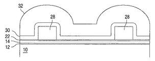
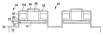
図2Eに示す構造体が、セルフ・アライン方法又は非セルフ・アライン方法のいずれかを使用して作られると、その構造体は、次のように更に処理される。図3Aないし3Uは、本発明のプロセスにおいて次のステップが実行されるときに図2B及び2Eに直交する方向から見た活性領域構造体17の断面図である。活性領域17の小さなセグメントしか示されていないが、以下に示す処理ステップは、このような領域のアレーを形成する。
最初に、絶縁層22が構造体上に形成される。より詳細には、酸化物層22がポリ層14の上に形成される(例えば、100ないし200Å厚み)。次いで、この酸化物層22の上に厚いポリ層24が形成される(例えば、3000Å厚みまで)。それにより得られる活性領域構造体が図3Aに示されている。
【0018】
従来のホトリソグラフィー(マスキング)スキムを次に使用して、半くぼみの第1トレンチ26が構造体に次のように形成される。適当なホトレジスト材料がポリ層24に付着され、そしてマスキングステップが実行されて、選択された平行な縞領域からホトレジスト材料が選択的に除去される(その下に第1のトレンチ26が形成される)。ホトレジスト材料が除去された場所では、露出されたポリシリコン24が、標準的なポリエッチングプロセス(例えば、酸化物層22をエッチングストッパーとして使用する非等方性ポリエッチング)を使用して除去され、ポリシリコンのブロック28が残され、それらの間に第1トレンチ26が形成される。ポリブロック28の巾は、使用するプロセスの最小リソグラフィー特徴部と同程度に小さなものでよい。残留ホトレジストが除去されて、図3Bに示す構造体が形成される。
【0019】
窒化物付着ステップを使用して、図3Cに示すように、構造体の上に窒化物層30が形成される(例えば、300ないし500Å厚み)。次いで、図3Dに示すように、窒化物層30の上に、厚い酸化物層32(例えば、2500Å厚み)が付着される。平坦化エッチングプロセスがそれに続き(例えば、化学的−機械的−ポリシング(CMP)エッチング)、これは、厚い酸化物層32を下方に、ポリブロック28の上部と一緒にエッチング除去する(ポリブロック28をポリシングストッパーとして使用して)。又、CMPエッチングは、ポリブロック28上の窒化物層30の部分も除去する。それにより生じる構造体が図3Eに示されている。
【0020】
ポリエッチングプロセスを使用して、ポリブロック28を除去し(酸化物層22をエッチングストッパーとして使用して)、第2のトレンチ34を形成する。制御された酸化物エッチングを使用して、第2のトレンチ34の底に露出された酸化物層22の部分を除去する(ポリ層14をエッチングストッパーとして使用して)。又、この酸化物エッチングは、厚い酸化物層32をある程度消費する。別のポリエッチングプロセスを実行して、第2のトレンチ34の底に露出されたポリ層14の部分を除去する(酸化物層12をエッチングストッパーとして使用して)。それにより生じる構造体が図3Fに示されている。
【0021】
熱酸化プロセスを使用してトレンチ34においてポリ層14の露出端に酸化物側壁層36が形成される。次いで、構造体の全表面にわたり適当なイオンインプランテーションが行われる。イオンは、それが各第2のトレンチ34において酸化物層12の露出部分に貫通するに充分なエネルギーをもつ場所では、周囲基板の導電型(例えばP型)とは異なる導電型(例えばN型)を有する基板10に第1領域(ソース領域)38を形成する。他の全ての領域では、イオンがその下の構造体により吸収され、何の作用も及ぼさない。インプランテーションされたソース領域38は、第2のトレンチ34にセルフ・アラインされる。次いで、側壁スペーサ40が第2のトレンチ34の壁に対して形成される。スペーサの形成は、公知であり、構造体の輪郭にわたって材料を付着し、その後、非等方性エッチングプロセスを実行し、それにより、構造体の水平面から材料を除去する一方、構造体の垂直方向を向いた表面では材料がほぼそのまま残される。スペーサ40は、窒化物層30及び基板シリコン10に対して良好なエッチング選択性をもつ任意の誘電体材料で形成することができる。好ましい実施形態では、絶縁スペーサ40は、全構造体上に薄い酸化物層(例えば、200Å)を付着し、その後、良く知られた反応性イオンエッチング(RIEドライエッチング)のような非等方性エッチングプロセスを行って、スペーサ40を除き付着酸化物層を除去することにより、酸化物で形成される。この酸化物エッチングプロセスは、第2のトレンチ34の底において酸化物層12の露出部分も除去し、基板10及び若干の酸化物層32を露出させる。それにより生じる構造体が図3Gに示されている。
【0022】
第2のトレンチには、好ましくは次のようにポリブロック42が埋められる。構造体の上にポリシリコンの厚い層が付着される。平坦化プロセス(即ちCMP)を使用して、第2のトレンチ34においてポリブロック42以外の付着ポリシリコンが除去される。ポリブロック42を互いに偶発的に短絡し得るトポグラフィーの問題がもしあれば、それに対処するために、任意のポリエッチングを行って、窒化物層30及び酸化物層32に対してポリブロック34の上面を若干くぼませることができる。ポリブロック42は、アレーの列を横切って延び(図2Cの1−1線に沿って)、そして基板10のソース領域38に直接電気的接触する。それにより得られる構造が図3Hに示されている。
【0023】
酸化物エッチングを使用して、酸化物層32が除去され、ポリブロック42間に配置された半くぼみの第3のトレンチ44が残される。次いで、従来の技術(例えば、LPCVD)により構造体上に酸化物層43が形成される(例えば、200ないし300Å)。それにより生じる構造体が図3Iに示されている。窒化物の厚い層(例えば、2000Å)を付着し、その後、非等方性窒化物(RIEドライ)エッチングを行って、スペーサ46(例えば、巾が1500Åまでのスペーサ)以外の付着窒化物を除去することにより、第3のトレンチ44の側壁に対して窒化物スペーサ46が形成される。それにより生じる構造体が図3Jに示されている。
【0024】
次いで、酸化物エッチングを使用して、酸化物層43の露出部分(即ち、スペーサ46によって保護されていない部分)が除去される。次いで、構造体は、熱酸化プロセスを受け、ポリブロック42上に酸化物層48が形成される。酸化物層48は、ポリブロック42に対してセルフ・アラインされる(例えば、600Åまでの厚みで)。この酸化プロセスの熱サイクル中に、ソース領域38は、基板へと深く押し入る。それにより得られる構造体が図3Kに示されている。
【0025】
非等方性(ドライ)窒化物エッチングを使用して、第3のトレンチに露出された(窒化物スペーサ46間で)窒化物層30の部分が除去される。このときは、酸化物層22がエッチングストッパーとして使用される。この窒化物エッチングは、ポリブロック42及びスペーサ46に隣接する窒化物層30の露出部分も若干除去する。非等方性酸化物エッチングがそれに続き、ポリ層14をエッチングストッパーとして使用して、第3のトレンチ44に露出された(窒化物スペーサ46間で)酸化物層22の部分が除去される。この酸化物エッチングは、酸化物層48の小さな部分も若干消費する。それにより生じる構造体が図3Lに示されている。
【0026】
非等方性(ドライ)ポリエッチングを次に実行し、酸化物層12をエッチングストッパーとして使用して、第3のトレンチに露出された(窒化物スペーサ46間で)ポリ層14の部分が除去される。非等方性(ドライ)酸化物エッチングがそれに続き、第3のトレンチに露出された(窒化物スペーサ46間で)酸化物層12の部分を除去し、第3のトレンチ44の底に基板10を露出させる。この酸化物エッチングは、酸化物層48の小さな部分も若干消費させる。それにより得られる構造体が図3Mに示されている。
【0027】
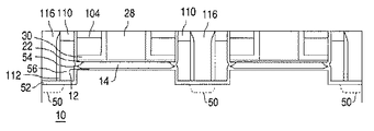
次いで、シリコン基板10が第3のトレンチ44の底に露出されたままの状態で、シリコンエッチングプロセスを実行して、第3のトレンチ44を基板10へと下方に延長する(例えば、基板表面より下へ500ないし1500Åの深さまで)。次いで、酸化物エッチングを使用して、酸化物層48を除去し、そして分離酸化物20a又は20b(図2Eに示す)の上部を、トレンチ44の底にほぼ等しいレベルまで下方にエッチングする。従って、第3のトレンチ44が連続的に形成され、そして活性及び分離領域17/16を横切って延びる。構造体の表面全体にわたって適当なイオンインプランテーションが再び実行される。このイオンインプランテーションは、基板10の活性領域において第3のトレンチ44の下に第2領域50(埋設ビットラインドレイン領域)を形成する。又、イオンインプランテーションは、露出したポリブロック42をドーピングする(又は更にドーピングする)という作用も有する。第3のトレンチ44の外側で、且つポリブロック42を除いて、イオンが阻止されそして何の作用も果たさない。それにより生じる構造体が図3Nに示されている。第2の領域50は、分離領域内にある第3のトレンチの部分の下には形成されない。というのは、分離酸化物20a又は20bによってイオンが阻止されるからである。
【0028】
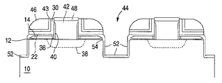
次いで、酸化プロセスが実行され、第3のトレンチ44の露出したシリコン表面を酸化して、これらシリコン表面のライナーとなる薄い酸化物層52が形成される。この酸化プロセスは、第3のトレンチ44の上部の側壁の一部分を形成するポリ層14の露出側縁14aも酸化し、水平に向けられたエッジ54を形成する。各エッジは、図3Oに示すように、第3のトレンチ44の側壁の1つに直接的に向けられる。エッジ54は、細長いエッジ(即ち、かみそりの刃の鋭いエッジのような)であってもよいし、又は短いエッジ(即ち、鉛筆の先端のような)であってもよい。又、この酸化プロセスは、ポリブロック42上に酸化物層48を再成長させる。
それに続き、第3のトレンチ44の側壁に沿ってポリスペーサ56が形成され、これは、構造体上にポリ層を最初に付着する(例えば、2000Å厚み)ことにより行われる。次いで、乾式の非等方性ドライエッチングプロセスを使用して、第3のトレンチ44の側壁に沿って残されるポリスペーサ56を除き、付着されたポリ層が除去される。それにより生じる構造体が図3Pに示されている。
【0029】
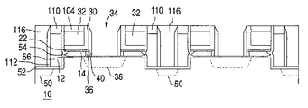
次いで、窒化物エッチングプロセスを使用して、窒化物スペーサ46が除去される。酸化物エッチングがそれに続き、酸化物層48及び43が除去されると共に、図3Qに示すように、第3のトレンチ44の底にある(ポリスペーサ56間において)酸化物層52の露出部分が除去される。窒化物エッチングプロセスがそれに続き(例えば、高温の燐酸において)、図3Rに示すように、窒化物層30が除去される。構造体上に酸化物層を付着し(例えば、500ないし1200Å厚み)、その後、酸化物エッチング(例えば、RIE)を行うことにより、第3のトレンチの側壁の底に沿って絶縁スペーサ58(好ましくは酸化物)が形成される。又、この酸化物付着及びエッチングプロセスは、ポリスペーサ56に隣接して(ポリエッジ54の上に)酸化物スペーサ60を形成すると共に、酸化物スペーサ40に隣接して酸化物スペーサ62を形成する。これにより生じる構造体が図3Sに示されている。
【0030】
次いで、金属付着ステップが実行され、タングステン、コバルト、チタン、ニッケル、白金、又はモリブデンのような金属が構造体上に付着される。次いで、構造体がアニールされ、高温の金属を第3のトレンチ44の底において基板10の露出部分へ流し込み且つ浸透させて、酸化物スペーサ58間に金属化シリコンの導電層64(シリサイド)を形成できるようにする。基板10における金属化シリコン領域64は、スペーサ58によって第2領域50にセルフ・アラインされるので、セルフ・アラインシリサイド(即ち、サリサイド)と称することができる。又、高温金属は、ポリスペーサ56の露出した上部に金属化ポリシリコンの導電層66(ポリサイド)を形成すると共に、ポリブロック42の露出した上部にポリサイド層68を形成する。残留構造体に付着した金属は、金属エッチングプロセスにより除去される。それにより生じる構造体が図3Tに示されている。
【0031】
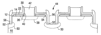
BPSG70のようなパッシベーションを使用して構造体をカバーし、これは第3のトレンチ44を埋めることを含む。マスキングステップを実行して、サリサイド領域64の上にエッチング領域が画成される。このエッチング領域においてBPSG70が選択的にエッチングされ、理想的にはサリサイド領域64(及び第2領域50)を中心とする接触開口が形成される。この接触開口には、次いで、金属付着及び平坦化エッチバックにより導体金属が埋められ、導体コンタクト72を形成する。サリサイド層64は、導体72と第2領域50との間の導通を向上させる。ポリサイド層66/68は、ポリスペーサ56及びポリブロック42の長さに沿った導通を向上させる。ビットラインコネクタ74がBPSG70上の金属マスキングによって各活性領域に追加され、その活性領域において全てのコンタクト72を一緒に接続する。最終的な構造が図3Uに示されている。
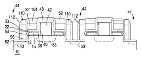
【0032】
図3Uに示すように、第1及び第2の領域38/50は、各セルのソース及びドレインを形成する(ソース及びドレインは動作中に交換できることが当業者に知られているが)。ポリ層14は、フローティングゲートを構成し、そしてポリスペーサ56は、各メモリセルの制御ゲートを構成する。各メモリセルのチャンネル領域76は、ソース及びドレイン38/50間の基板の表面部分である。各チャンネル領域76は、互いに直角に接合された2つの部分、即ち第3のトレンチ44の垂直壁に沿って延びる垂直部分78と、第3のトレンチ44とソース領域38との間に延びる水平部分80とを有する。各フローティングゲート14は、チャンネル領域76の水平部分80と、ソース領域38の一部分の上に配置されるが、そこから絶縁される。フローティングゲート14は、各々、水平に向けられたエッジ54を有し、これは、制御ゲート56の1つに直接対面するが、酸化物層52によりそこから絶縁される。本発明のプロセスは、互いに鏡像関係のメモリセルの対を形成し、第3のトレンチ44の各側にメモリセルが形成されて、共通のビットライン領域50を共有する。同様に、ポリブロック42に電気的に接触する各ソースライン領域38が、隣接メモリセル間で、異なる鏡像セットのメモリセルから共有される。各制御ゲート56、ソース領域38(ポリブロック42が電気的に接続された)及びドレイン領域50は、分離領域16及び活性領域17を横切って連続的に延び、各活性領域17から1つのメモリセルを一緒にリンクする。
【0033】
メモリセルの動作
図3Uを参照してメモリセルの動作を以下に説明する。このようなメモリセルの動作及び動作理論は、米国特許第5,572,054号にも開示されており、フローティングゲート及び制御ゲートを有する不揮発性メモリセルを消去し及び読み取る動作及び動作理論、フローティングゲートから制御ゲートへのトンネル作用、並びにこのようなメモリセルのアレーについては、その開示を参考としてここに援用する。
【0034】
所与の活性領域17において選択されたメモリセルを最初に消去するために、そのソース38及びドレイン50の両方に接地電位が印加される。制御ゲート56には、高い正の電圧(例えば、+5ないし10ボルト)が印加される。フローティングゲート14の電子は、酸化物層52を経て制御ゲート56へとトンネル通過するファウラー−ノルドハイムトンネリングメカニズムによって誘起され、フローティングゲート14を正に荷電したままにする。このトンネリングは、各フローティングゲート14に形成された水平に向いたエッジ54により改善される。各制御ゲート56は、活性領域17及び分離領域16を横切って連続的に延びるので、制御ゲート56の1つに高電圧が印加されると、各活性領域から1つのメモリセルが消去されることに注意されたい。
【0035】
選択されたメモリセルをプログラミングすることが望まれるときには、小さな電圧(例えば、0.5ないし1.0V)がそのドレイン領域50に印加される。制御ゲート56により画成されたMOS構造体のスレッシュホールド電圧付近の正の電圧レベル(約+1.8ボルト程度)がその制御ゲート56に印加される。そのソース領域38には、9又は10ボルト程度の正の高い電圧が印加される。ドレイン領域50により発生された電子は、ドレイン領域50から、チャンネル領域76の弱く反転した垂直部分78を経てソース領域38に向かって流れる。これらの電子は、チャンネル領域76の水平部分80に到着すると、フローティングゲート14の近方端の高い電位を見る(フローティングゲート14は、制御ゲート56よりも、正に荷電されたソース領域38に強く容量性結合されているために)。電子は加速しそして加熱され、そのほとんどが絶縁層12へ注入されそして絶縁層を貫通してフローティングゲート14へと注入される。接地電位及びVdd(デバイスの電源電圧に基づき約1.5ないし3.3ボルト)が、選択されたメモリセルを含まないメモリセルの行及び列に対し、ソースライン38及びビットライン領域50に各々印加される。選択されたメモリセルを含まないメモリセルの行に対し制御ゲート56に接地電位が印加される。従って、選択された行及び列のメモリセルのみがプログラムされる。
【0036】
フローティングゲート14への電子の注入は、フローティングゲート14の近方端における電荷の減少が、熱電子を発生するための高い表面電位を水平チャンネル領域部分80に沿ってもはや維持できなくなるまで続く。その点において、フローティングゲート14の減少された電荷が、ドレイン領域50からフローティングゲート14への電子の流れを減少する。
【0037】
最後に、選択されたメモリセルを読み取るために、接地電位がそのソース領域38に印加される。約+1ボルトの読み取り電圧がそのドレイン領域50に印加され、そして約1.5ないし3.3ボルト(デバイスの電源電圧に基づく)がその制御ゲート56に印加される。フローティングゲート14が正に荷電された(即ち、フローティングゲートの電子が放電した)場合には、チャンネル領域76の水平部分80(フローティングゲート14の真下の)がターンオンされる。制御ゲート56が読み取り電位まで上昇すると、チャンネル領域76の垂直部分78(制御ゲート56に直接隣接する)もターンオンされる。従って、全チャンネル領域76がターンオンし、ソース領域38からドレイン領域50へ電流を通流させる。これは、「1」状態となる。
【0038】
一方、フローティングゲート14が負に荷電された場合には、チャンネル領域76の水平部分80(フローティングゲート14の真下)が弱くターンオンするか、又は完全にシャットオフする。制御ゲート56及びドレイン領域50が読み取り電位まで上昇しても、チャンネル領域76の水平部分80にはほとんど又は全く電流が流れない。この場合に、電流が「1」状態に比して非常に僅かであるか、又は全く電流が流れない。このようにして、メモリセルは、「0」状態でプログラムされるセンスとされる。非選択の列及び行に対してソースライン38、ビットライン領域50及び制御ゲート56に接地電位が印加され、従って、選択されたメモリセルだけが読み取られる。
【0039】
メモリセルアレーは、良く知られた従来の行アドレスデコード回路、列アドレスデコード回路、センス増幅回路、出力バッファ回路及び入力バッファ回路を含む周辺回路を備えている。
本発明のメモリセルアーキテクチャーは、フローティングゲートの上方に延びるエッジと制御ゲートとの間に垂直方向に重畳する限定領域を使用しないので、効果的である。図1の公知構成に示したように、フローティングゲート1と制御ゲート5との間には第1の結合キャパシタンスC1が横方向にあり、そしてフローティングゲート1と制御ゲート5との間には第2の結合キャパシタンスC2が垂直方向にある。その目標とするところは、これら2つの素子間の容量性結合を最小にしながらトンネリングの効率を最大にすることである。C2は、フローティングゲート1の上に張り出した制御ゲート5の量を減少することにより最小にすることができる。しかしながら、フローティングゲートは、製造プロセスの制約により一定厚みを有するので、C1を最小にするには制約がある。C1を減少するためにフローティングゲートと制御ゲートとの間の横方向距離を増加する場合には、それらの間の絶縁材料がトンネル作用により質低下される。トンネル作用を向上するために横方向距離を狭くした場合には、容量性結合C1が大きくなる。従って、容量性結合C1がスケーリング限界として働く。
【0040】
しかしながら、本発明では、このスケーリング限界がバイパスされる。というのは、水平に向けられたエッジ54が、その横方向に隣接して配置された垂直に向けられた制御ゲートスペーサ56に直接対向するからである。垂直に向けられた容量性結合(例えばC2)はなく、そして横方向に向けられた容量性結合(例えばC1)は充分に小さいが、水平に向けられたエッジ54と制御ゲート56との間には依然充分なトンネリングを生じさせることができる。
【0041】
本発明は、サイズが減少されそしてプログラム効率が優れたメモリセルアレーも提供する。メモリセルのサイズは、50%程度減少される。というのは、ビットライン領域50が基板10内に埋設され、そしてビットライン領域50が第3のトレンチとセルフ・アラインされ、そこでは、リソグラフィー発生、接触整列及び接触完全性の制約によりスペースが浪費されることがない。本発明では、0.18μm及び0.13μmの技術世代を各々使用して約0.21μm及び0.14μmのセル領域を得ることができる。プログラム効率は、チャンネル領域76の垂直部分78をフローティングゲート14に「照準」することによって大幅に改善される。従来のプログラミング構成では、チャンネル領域の電子がフローティングゲートの平行な経路に流れ、そこで、比較的少数の電子が加熱されそしてフローティングゲートに注入される。推定プログラム効率(全電子数に対する注入電子数)は、約1/1000と推定される。しかしながら、チャンネル領域の第1部分は、フローティングゲートに直接「照準」される電子経路を定義するので、本発明のプログラム効率は、ほぼ全部の電子がフローティングゲートに注入される1/1付近であると推定される。
【0042】
又、本発明では、第3のトレンチ44の側壁に沿って形成される制御ゲートは、セルのサイズに影響せずに、導通性能及びパンチスルー余裕度に対して別々に最適化することができる。更に、ソース領域38と埋設ビットライン領域50との間のパンチスルー抑制は、第1導電型(例えば、N型)を有するソース領域を、その第1導電型とは異なる第2導電型(例えば、P型)を有するウェルに埋設すると共に、メモリセルの導通特性に影響しない他のサブ表面インプラントを使用することにより、最適化することができる。更に、ソース領域38及びビットライン領域50を垂直方向及び水平方向に分離すると、セルサイズに影響なく、信頼性パラメータを容易に最適化することができる。
【0043】
最後に、本発明のメモリセル構造体は、「持ち上がったソースライン」42を備え、これは、導電性ポリブロック42がソースライン38に沿って延びる(及びそれに電気的に接続される)が、基板表面より上に配置されることを意味する。持ち上がったソースライン42は、それらの側壁がフローティングゲート14の側壁に横方向に隣接して配置されるが、酸化物層36及び酸化物スペーサ40によってそこから絶縁されている。この構成は、ソースライン38の長さに沿って電気的抵抗の減少を与え、そして持ち上がったソースライン42とフローティングゲート14との間に容量性結合を与える(フローティングゲート14とソース領域38との間の重畳により生じる容量性結合に加えて)。
本発明では、ポリブロック42がソース領域38にセルフ・アラインされ、そしてフローティングゲート14がポリブロック42と制御ゲートのポリスペーサ56との間にセルフ・アラインされる(従って、チャンネル領域76の第1及び第2部分78/80にセルフ・アラインされる)。
【0044】
第1の別の実施形態
図4Aないし4Gは、図3Uに示したものと同様のメモリセル構造体を形成するための第1の別のプロセスを示し、この場合には、窒化物層30を除去するために使用される窒化物エッチングが、窒化物層の一部分を保存するためにプロセスにおいて後で実行される。この第1の別のプロセスは、図3Oに示された同じ構造体で始まり、これは、図4Aに再び示されている。
【0045】
第3のトレンチ44の側壁に沿ったポリスペーサ56の形成は、図3Pを参照して上述したのと同様に行われるが、好ましくは薄いポリ層が構造体上に付着され(例えば、700Å厚み)、その後、乾式非等方性ドライエッチングプロセスを行い、第3のトレンチ44の側壁に沿って残されたポリスペーサ56を除いて、付着ポリ層を除去する。各ポリスペーサ56の上縁が、その隣接窒化物層30の上縁とほぼ水平になる(図4Bに示すように)か、又は隣接するフローティングゲートのエッジ54と窒化物層30の隣接上縁との間に位置するよう確保するためにポリエッチングが実行されるのが好ましい。
【0046】
次いで、窒化物エッチングプロセスを使用して、窒化物スペーサ46が除去される。酸化物エッチングがそれに続き、酸化物層48及び43が除去されると共に、図4Cに示すように、第3のトレンチ44の底において(ポリスペーサ56間にある)酸化物層52の露出部分が除去される。絶縁スペーサ58(好ましくは酸化物)は、構造体上に酸化物の層を付着し(例えば、500ないし1200Å厚み)、その後、酸化物エッチング(例えば、RIE)を行うことにより、第3のトレンチ44の側壁に沿って形成される。又、この酸化物付着及びエッチングプロセスは、窒化物層30の垂直部分に隣接して酸化物スペーサ62を形成する。それにより得られる構造体が図4Dに示されている。
【0047】
次いで、金属付着ステップが実行されて、タングステン、コバルト、チタン、ニッケル、白金又はモリブデンのような金属が構造体上に付着される。次いで、構造体がアニールされ、高温の金属を第3のトレンチ44の底において基板10の露出部分へ流し込み且つ浸透させて、サリサイド層64を形成することができる。又、高温金属は、ポリスペーサ56の露出した上部にポリサイド層66を形成すると共に、ポリブロック42の露出した上部にポリサイド層68を形成する。残留金属を除去するための金属エッチングプロセスの後に得られる構造体が、図4Eに示されている。
【0048】
窒化物エッチングプロセスがそれに続き(例えば、高温の燐酸において)、図4Fに示すように、窒化物層30の露出部分(即ち酸化物スペーサ62により保護されない部分)を除去する。この構造体は、図3Uを参照して述べたように処理され(即ち、パッシベーション、接触形成及びビットライン形成)、図4Gに示す構造体が得られる。
【0049】
図3Aないし3Uのプロセスからのこの第1の別の実施形態の主たる相違は、窒化物層30を除去するための窒化物エッチングステップがプロセスにおいて後で実行されることである。その結果、窒化物層30は、サリサイド/ポリサイド金属化プロセス中に酸化物層22(フローティングゲート14の上の)を保護するためにそのまま残される。更に、窒化物層30の一部分は、最終的なメモリセル構造体においてそのまま残される(フローティングゲート14の上で且つポリブロック42に横方向に隣接して)。窒化物の高い誘電率(酸化物に比して)が与えられると、窒化物層30のこの残留部分は、より強力な側壁フリンジフィールドを与え、従って、メモリセルの各々に対しソース領域38(ポリブロック42を含む)とフローティングゲート14との間の容量性結合を改善する。
【0050】
第2の別の実施形態
図5Aないし5Iは、図3Uに示されたものと同様のメモリセル構造体を形成するための第2の別のプロセスを示し、この場合には、第2の領域50を形成するのに使用されるイオンインプランテーションがプロセスにおいて後で実行されそして付加的なトンネル酸化物の形成が含まれる。この第2の別のプロセスは、図3Mに示されたものと同じ構造で始まり、これは図5Aに再び示されている。
【0051】
同じシリコン及び酸化物エッチングプロセスが図3Nを参照して述べたように実行され、図5Bに示すように、第3のトレンチ44が基板10へと下方に拡張され、そして酸化物層48が除去される。しかしながら、第2領域50を形成するのに使用されるイオンインプランテーションは、このときには実行されない。むしろ、図3Oを参照して述べた酸化プロセスが実行されて、図5Cに示すように、酸化物層52及びフローティングゲートのエッジ54が形成され、そして酸化物層48が再成長される。
【0052】
制御型酸化物エッチングプロセス(例えば、10対1に希釈されたHFエッチング剤を伴う)が実行されて、酸化物層52が除去され、そしてフローティングゲートの鋭いエッジ54が露出される。薄い酸化物層82(例えば、130Å)が構造体上に付着される(例えば、HTO付着により)。酸化物層52を除去しそして酸化物層82を付着すると、制御された厚みをもつトンネル酸化物層が鋭いエッジ54に隣接して形成される。次いで、ポリ層を構造体上に付着し(例えば、700Å厚み)、その後、乾式非等方性ドライエッチングプロセスを行って、第3のトレンチ44において酸化物層82に沿って残されるポリスペーサ56を除き付着ポリ層を除去することにより、ポリスペーサ56が第3のトレンチ44の側壁に沿って形成される。各ポリスペーサ56の上縁が、その隣接窒化物層30の上縁とほぼ水平になる(図5Dに示すように)か、又は隣接するフローティングゲートのエッジ54と窒化物層30の隣接上縁との間に位置するよう確保するために、ポリエッチングが実行されるのが好ましい。
【0053】
次いで、酸化物エッチングプロセスを使用し、酸化物層82の露出部分(即ちポリスペーサ56により保護されない部分)と、酸化物層48とが除去される。次いで、窒化物エッチングを使用して、窒化物スペーサ46が除去され、その後、酸化物エッチングにより、酸化物層43が除去される。それにより得られる構造体が図5Eに示されている。構造体の全表面にわたって適当なイオンインプランテーションが行われて、第3のトレンチ44の下で基板10に第2領域50(埋設ビットライン領域)が形成される。第3のトレンチ44の外側では、イオンが阻止され、何の作用も与えない。絶縁スペーサ58(好ましくは酸化物)は、構造体上に酸化物層を付着し(例えば、500ないし1200Å厚み)、その後、酸化物エッチング(例えば、RIE)を行うことにより第3のトレンチ44の側壁に沿って形成される。この酸化物付着及びエッチングプロセスは、窒化物層30の垂直部分に隣接して酸化物スペーサ62を形成する。それにより生じる構造体が図5Fに示されている。絶縁スペーサ58を形成した後、又は制御ゲート56を形成した後であってスペーサ46を除去する前に、イオンインプランテーションプロセスを実行できることに注意されたい。
【0054】
熱アニールプロセス(例えば、RTA又は炉熱アニール)を使用して、第1及び第2領域38/50が基板10の深部へ押し込まれる。次いで、金属付着ステップが実行されて、タングステン、コバルト、チタン、ニッケル、白金又はモリブデンのような金属が構造体上に付着される。次いで、構造体がアニールされて、サリサイド領域64を形成し(第3のトレンチ44の底において酸化物スペーサ58間に)、ポリサイド領域66を形成し(ポリスペーサ56の露出上部の上に)、そしてポリサイド領域68を形成する(ポリブロック42の露出上部に)。残留構造体に付着された金属は、金属エッチングプロセスにより除去される。それにより得られる構造体が図5Gに示されている。
【0055】
窒化物エッチングプロセスがそれに続き(例えば、高温の燐酸において)、図5Hに示すように、窒化物層30の露出部分(即ち酸化物スペーサ62により保護されない部分)を除去する。この構造体は、次いで、図3Uを参照して述べたように処理され(即ち、パッシベーション、接触形成及びビットライン形成)、図5Iに示す構造体が得られる。
【0056】
この第2の別の実施形態は、第2領域50を形成するのに使用されるイオンインプランテーションステップを、制御ゲートのスペーサ56が形成された後までシフトする。フローティングゲートのエッジ54と制御ゲート56との間のトンネリングに使用される酸化物層82は、熱成長ステップではなく、酸化物付着ステップ(例えば、HTO)により形成され、第3のトレンチ44の輪郭により誘起されるストレスが与えられると、良好に均一性を達成する。最後に、窒化物層の残留部分は、より強力な側壁フリンジフィールドを与え、ひいては、ソース領域38(ポリブロック42を含む)とフローティングゲート14との間の容量性結合を改善する。
【0057】
第3の別の実施形態
図6Aないし6Jは、図3Uに示したものと同様のメモリセル構造体を形成するための第3の別のプロセスを示し、これは、「L」字型の制御ゲート及びチャンネル領域を備え、その各々は、2つの個別の水平部分が垂直部分で分離されたものを有している。この第3の別のプロセスは、図3Mに示されたものと同じ構造体で始まり、これは、図6Aに再び示されている。
【0058】
図3Nを参照して述べたように、同じエッチングプロセスが実行されて、図6Bに示すように、第3のトレンチ44を基板10へと下方に拡張する。しかしながら、第2領域50を形成するのに使用されるイオンインプランテーションは、このときには実行されない。むしろ、図3Oを参照して述べた酸化プロセスが実行されて、図6Cに示すように、酸化物層52及びフローティングゲートのエッジ54が形成される。
ポリ層84が構造体上に形成される。ポリ層84の上面に任意のポリサイド層86が形成され、上述した金属付着及びアニールプロセスが行われる。層84及び86の全厚みは、約700Åであるのが好ましい。次いで、酸化物層が構造体上に形成され、その後、酸化物エッチングが行われ、第3のトレンチ44においてポリ層84に対して形成された酸化物スペーサ58を除き、酸化物層が除去される。それにより生じる構造体が図6Dに示されている。
【0059】
ポリエッチングプロセスを使用して、ポリサイド層86及びポリ層84の露出部分(即ち、酸化物スペーサ58により保護されない部分)が除去され、トレンチ44の側壁及び底壁に沿ってポリ及びポリサイド層84/86の「L」字型セグメントが残される。このポリエッチング、及び酸化物スペーサ58の形成は、各ポリ/ポリサイドセグメント84/86の上縁が、その隣接窒化物層30の上縁とほぼ水平になる(図6Eに示すように)か、又は隣接するフローティングゲートのエッジ54と窒化物層30の隣接上縁との間に位置するよう確保するために行われるのが好ましい。
【0060】
窒化物エッチングプロセスは、露出された窒化物スペーサ46を除去するのに使用される。次いで、酸化物エッチングが使用されて、図6Fに示すように、酸化物スペーサ58(第3のトレンチ44における)、酸化物層48(ポリブロック42上の)、酸化物層43、及び酸化物層52の部分(第3のトレンチ44の底においてポリセグメント84間にある)が除去される。酸化物付着及びエッチバックプロセス(例えば、RIEドライエッチング)を使用して、酸化物スペーサ88を形成し(第3のトレンチ44において層52、84及び86の露出され垂直に向けられた端部に対して)、酸化物スペーサ90を形成し(第3のトレンチ44においてポリサイド層86の垂直に向けられた部分に対して)、そして酸化物スペーサ92を形成する(窒化物層30の垂直に向けられた部分に対して)。構造体の全表面にわたって適当なイオンインプランテーションを行って、第3のトレンチ44の下で基板10に第2領域50(埋設ビットライン領域)を形成する。又、ポリブロック42にもイオンインプランテーションされて、これらブロックがドープ(又は更にドープ)される。第3のトレンチ44の外側の領域では、ポリブロック42を除き、イオンが阻止され、何の作用も及ぼさない。イオンインプランテーションプロセスは、酸化物スペーサ88/90/92を形成する前に行うこともできるし、又は窒化物スペーサ46を除去する前に行うこともできる点に注意されたい。それにより得られる構造が図6Gに示されている。
【0061】
次いで、金属付着ステップが行われて、タングステン、コバルト、チタン、ニッケル、白金又はモリブデンのような金属が構造体上に付着される。次いで、構造体がアニールされて、サリサイド領域64を形成し(第3のトレンチ44の底において酸化物スペーサ58間に)、ポリサイド領域94を形成し(ポリ層セグメント84の露出上部の上に)、そしてポリサイド領域68をポリブロック42の露出上部に形成する。残留構造体に付着された金属は、金属エッチングプロセスにより除去される。それにより得られる構造体が図6Hに示されている。
窒化物エッチングプロセスがそれに続き(例えば、高温の燐酸において)、図6Iに示すように、窒化物層30の露出部分(即ち酸化物スペーサ92により保護されない部分)を除去する。この構造体は、次いで、図3Uを参照して述べたように処理され(即ち、パッシベーション、接触形成及びビットライン形成)、図6Jに示す構造体が得られる。
【0062】
この第3の別の実施形態は、第2の領域50を形成するのに使用されるイオンインプランテーションステップを、ポリ層セグメント84及びポリサイド86の形成により第3のトレンチ44の底が狭められる後までシフトする。従って、第2領域50は、第3のトレンチの底壁の中央部分の下だけに形成される。これは、ほぼ直角に接合された3つの部分を有する各セルに対して基板にチャンネル領域76を形成し、即ち第1の水平部分80は、第3のトレンチ44とソース領域38との間に延び、垂直部分78は、第3のトレンチ44の垂直壁に沿って延び、そして第2の水平部分96は、垂直部分78とドレイン領域50との間に延び、従って、チャンネル領域76は、ほぼ「S」字型となる。窒化物層30の残りの部分は、より強力な側壁フリンジフィールドを与え、従って、ソース領域38(ポリブロック42を含む)とフローティングゲート14との間の容量性結合を改善する。最後に、制御ゲートの厚みは、正確に制御することが非常に困難なポリ付着及びエッチバックプロセスではなく、ポリ付着ステップによって指令される。
【0063】
第4の別の実施形態
図7Aないし7Zは、図3Uに示したものと同様のメモリセル構造体を、セルフ・アライン接触(SAC)構成を使用して形成するための第4の別のプロセスを示す。この第4の別のプロセスは、図3Cに示したものと同じ構造体で始まり、これは図7Aに再び示されている。
【0064】
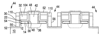
誘電体材料の厚い層102(例えば、BSG)が、図7Bに示すように構造体上に付着され、酸化物層32の部分間のギャップを埋める。BSGエッチングプロセスを使用して、BSG層102を、酸化物層32の上部とほぼ平らになるまで下方にエッチングし、このとき、酸化物層32をエッチングストッパーとして使用する。BSGエッチングプロセスは、図7Cに示すように、酸化物層32の上部間に配置されたBSG102のブロックを形成する。酸化物エッチングプロセスを使用して、酸化物層32の露出部分を、窒化物層30の上部とほぼ平らになるまで下方にエッチングし、このとき、窒化物層30をエッチングストッパーとして使用する。制御型酸化物オーバーエッチングを使用して、酸化物層32の露出部分を、図7Dに示すように、窒化物層30の上部から所定の距離だけ下へと下方にエッチングする。
【0065】
次いで、厚い窒化物層104が、図7Eに示すように、構造体上に付着される。平坦化エッチングプロセス(例えば、CMP)がそれに続き、窒化物層104、BSG102及び窒化物30を、ポリブロック28の上部と平らになるように下方にエッチングし(ポリブロック28をポリシングストッパーとして使用して)、そしてポリブロック28の上面を露出したままにする。それにより得られる構造体が図7Fに示されている。
ポリエッチングプロセスを使用して、ポリブロック28を除去し(酸化物層22をエッチングストッパーとして使用して)、第2のトレンチ34を形成する。制御型の酸化物エッチングを使用して、第2のトレンチ34の底に露出した酸化物層22の部分を除去する(ポリ層14をエッチングストッパーとして使用して)。別のポリエッチングプロセスを実行して、第2のトレンチ34の底に露出したポリ層14の部分を除去する(酸化物層12をエッチングストッパーとして使用して)。それにより生じる構造体が図7Gに示されている。
【0066】
トレンチ34において熱酸化プロセスを使用してポリ層14の露出端に酸化物側壁層36が形成される。次いで、適当なイオンインプランテーションを使用し、周囲基板の導電型(例えばP型)とは異なる導電型(例えばN型)を有する基板10に第1領域(ソース領域)38が形成される。次いで、全構造体上に薄い酸化物層(例えば、200Å)を付着し、その後、非等方性エッチングプロセス(例えば、RIEドライエッチング)を行って、スペーサ40以外の付着酸化物層を除去することにより、第2のトレンチ34の壁に側壁スペーサ40が形成される。又、この酸化物エッチングプロセスは、第2のトレンチ34の底において酸化物層12の露出部分も除去し、基板10を露出させる。それにより得られる構造体が図7Hに示されている。
【0067】
第2のトレンチがポリブロック42で埋められ、これは、構造体上にポリシリコンの厚い層を付着し、その後、平坦化プロセス(即ちCMP)を行って、第2のトレンチ34においてポリブロック42を除き付着ポリシリコンを除去することにより行われるのが好ましい。任意のポリエッチングを実行して、窒化物層104及び酸化物層32に対してポリブロック42の上面を若干くぼませ、トポロジーの問題がもしあれば、それに対処する。ポリブロック42は、基板10のソース領域38と直接電気的接触し、そしてその場でドープすることもできるし又は個別のインプランテーションによってドープすることもできる。それにより得られる構造体が図7Iに示されている。
【0068】
BSGエッチングプロセス(湿式又は乾式)を使用して、BSG102が除去され、酸化物層32の一部分が露出される。次いで、非等方性エッチング(例えば、RIE)を使用して、酸化物層32の露出部分(即ち、窒化物104により保護されない部分)を除去し、図7Jに示すように、酸化物ブロック32間に露出された半くぼみの第3のトレンチ44を残す。
次いで、構造体は、熱酸化プロセスを受け、ポリブロック12上に酸化物層48が形成される。この酸化物層48は、ポリブロック42とセルフ・アラインされる(例えば、600Åまでの厚みで)。この酸化プロセスの熱サイクル中に、ソース領域38は、基板へと深く押し込まれる。それにより生じる構造体が図7Kに示されている。
【0069】
非等方性(乾式)窒化物エッチングを使用して、第3のトレンチに(酸化物ブロック32間で)露出された窒化物層30の部分を除去し、このとき、酸化物層22をエッチングストッパーとして使用する。又、この窒化物エッチングは、ポリブロック42に隣接した窒化物層30の露出部分もある程度除去し、そして窒化物層104の厚みを減少する(例えば、300ないし500Åまでの厚みに)。非等方性酸化物エッチングがそれに続き、ポリ層14をエッチングストッパーとして使用して、第3のトレンチ44に(酸化物ブロック32間で)露出された酸化物層22の部分を除去する。又、この酸化物エッチングは、酸化物層48の小さな部分を若干消費する。それにより生じる構造体が図7Lに示されている。
【0070】
非等方性(乾式)ポリエッチングを次いで実行して、酸化物層12をエッチングストッパーとして使用して、第3のトレンチに(酸化物ブロック32間で)露出されたポリ層14の部分を除去する。このポリエッチングは、図7Mに示すように、第3のトレンチ44に面するポリ層14の縁に傾斜即ちテーパー領域106を形成するように実行されるのが好ましい。
【0071】
非等方性(乾式)酸化物エッチングがそれに続き、第3のトレンチに(酸化物ブロック32間で)露出された酸化物層12の部分が除去されて、第3のトレンチ44の底において基板10を露出させる。又、この酸化物エッチングは、酸化物層48の小さな部分を若干消費する。それにより生じる構造体が図7Mに示されている。次いで、シリコン基板10が第3のトレンチ44の底に露出されたままである状態で、シリコン(乾式)エッチングプロセスが実行されて、第3のトレンチ44を、基板表面より500Åないし1500Å低い深さまで、基板10へと下方に拡張する。このエッチングは、シリコンと酸化物との間で1対1の選択性をもつように選択され、従って、酸化物分離領域16にも同様の深さのトレンチをエッチングし(LOCOS又はSTI)、ここでは、第3のトレンチ44が連続的に形成されそして活性及び分離領域17/16を横切って延びる。それにより生じる構造体が図7Nに示されている。
【0072】
次いで、酸化プロセスが実行され、第3のトレンチ44の露出シリコン面が酸化されて、これらシリコン面のライニングとなる薄い酸化物層52(例えば、150Å)が形成される。又、この酸化プロセスは、第3のトレンチ44の上部の側壁の一部分を形成するポリ層14の露出テーパー面106も酸化し、図7Oに示すように、第3のトレンチ44の側壁の1つを各々直接的に指す水平に向けられたエッジ54を形成する。エッジ54は、細長いエッジでもよいし(即ちかみそりの刃の鋭いエッジのような)、又は短いエッジ(鉛筆の先端のような)でもよい。又、この酸化プロセスは、酸化物層48をポリブロック42より厚くする。
【0073】
任意の酸化物層最適化プロセスが次に行われ、第3のトレンチ44から酸化物層52を除去し、その後、HTO酸化物付着ステップを行って、良好に制御された厚み(例えば、150Å)を有する酸化物層52を全構造体上に再形成することにより、熱成長ファウラー−ノルドハイムトンネリング酸化物の厚みを最適化することができる。それにより生じる構造体が図7Pに示されている。
図7Qに示すように、ポリ層56が構造体上に形成される(例えば、800Å厚み)。ポリ層56の上面には、金属化ポリシリコン(図示せず)を形成することができる。次いで、図7Rに示すように、ポリ層56上に、誘電体材料の層108(例えば、BSG、1000Åまで)が形成される。次いで、BSGエッチングプロセスを使用して、BSG108を、酸化物層52と平らになるように下方にエッチングし、その後、ポリエッチングにより、ポリ層56を、酸化物層52と平らになるように下方にエッチングする。これらBSG及びポリエッチングに代わって、CMP平坦化を使用することもできる。付加的なポリエッチングを行って、図7Sに示すように、ポリ層56の上部を酸化物層52の上部及びBSG108より下にくぼませる。
【0074】
次いで、窒化物層110が、図7Tに示すように、構造体上に付着される(例えば、800Å)。その後、窒化物エッチングが、酸化物層52をエッチングストッパーとして使用して行われ、図7Uに示すように、ポリ層56の上に窒化物ブロック110を残す。窒化物ブロック110は、酸化物層52(及び酸化物ブロック32)と、BSG108とにより、ポリ層56にセルフ・アラインされる。次いで、BSGエッチングを使用して、第3のトレンチ44からBSGブロック108が除去される。それにより生じる構造体が図7Vに示されている。
【0075】
非等方性ポリエッチングを使用して、図7Wに示すように、第3のトレンチ44の底においてポリ56の露出部分(窒化物110により保護されない部分)が除去される。次いで、窒化物が構造体上に付着され(例えば、300Å厚み)、その後、非等方性窒化物エッチング(例えば、RIE)を実行し、第3のトレンチ44において窒化物スペーサ112を除き付着窒化物が除去される。構造体の全面にわたって適当なイオンインプランテーションがもう一度行われ、第3のトレンチ44の下で基板10に第2領域50(埋設ビットラインドレイン領域)が形成される。第3のトレンチ44の外部では、イオンが阻止され、何の作用も果たさない。イオンインプランテーションプロセスは、酸化物エッチングが次に行われた後に実行できることに注意されたい。それにより生じる構造体が図7Xに示されている。
【0076】
酸化物エッチングステップが次に行われて、酸化物層52及び酸化物層48の露出部分が除去される。次いで、金属付着ステップが行われて、タングステン、コバルト、チタン、ニッケル、白金、又はモリブデンのような金属が構造体上に付着される。次いで、構造体がアニールされて、酸化物スペーサ112間で露出基板に金属化シリコン64(シリサイド)の導電層が形成され、そしてポリブロック42の露出した上部に金属化ポリシリコン66(ポリサイド)の導電層が形成される。残りの構造体に付着された金属は、金属エッチングプロセスにより除去される。それにより得られる構造体が図7Yに示されている。
【0077】
酸化物層114(例えば、BP TEOS)を使用して、構造体がカバーされる。マスキングステップを実行して、サリサイド領域64の上にエッチング領域が画成される。このエッチング領域において酸化物層114が選択的にエッチングされ、理想的にはサリサイド領域64(及び第2領域50)を中心とする接触開口が形成される。次いで、接触開口には、金属付着及び平坦化エッチバックにより導体金属が埋められ、導体コンタクト72を形成する。サリサイド層64は、導体72と第2領域50との間の導通を改善する。ポリサイド層66は、ポリブロック42の長さに沿った導通を改善する。酸化物114上に金属マスキングを行うことにより各活性領域にビットラインコネクタ74が追加され、その活性領域において全てのコンタクト72が一緒に接続される。最終的な構造が図7Zに示されている。
【0078】
コンタクト72の形成は、セルフ・アライン型接触構成(SAC)と称される。というのは、コンタクトの巾が、隣接対向窒化物スペーサ112間の分離距離より広くされ、従って、ドレイン領域50にセルフ・アラインされるからである。コンタクト72の一部分は、ポリブロック56の真上に形成されるが、窒化物層110によりそこから絶縁され、従って、ドレイン領域50との良好な接触が得られるように確保する。
【0079】
セルフ・アライン型接触構成(SAC)は、対構成のメモリセルの隣接セット間の最小間隔要件に関する重要な制約を排除する。より詳細には、図7Zは、好ましくはドレイン領域50を中心とする接触領域(従って、導体72)を示しているが、実際には、ドレイン領域50に対してある程度の望ましくない水平シフトなしに接触開口を形成することが非常に困難である。コンタクト72がスペーサ112間の空間を完全に埋めるのを妨げるに充分なほど水平シフトが大きくなった場合には、欠陥接続が発生する。図3Uに示した実施形態に使用されるような非セルフ・アライン接触構成では、ポリスペーサ56上に窒化物の保護層がないところでは、コンタクト72がシフトしてポリスペーサ56と接触した場合に、電気的な短絡が生じ得る。非セルフ・アライン接触構成において電気的な短絡を防止するために、接触開口にはスペーサ58から充分離れたエッジが形成され、したがって、接触領域において考えられる最大のシフトがあっても、それらがスペーサ58を越えて延びることはない。これは、もちろん、図3Uに示した実施形態に対しスペーサ58間の最小距離に関する制約を与え、対構成の鏡像セルの隣接セット間に充分な許容距離がとれるようにする。
【0080】
第4の別の実施形態で使用されるSACは、ポリブロック56上に保護材料層(窒化物層110)を使用することによりこの制約を排除する。この保護層があると、形成中に接触開口が著しく水平にシフトしても、接触開口とドレイン領域50の重畳を確保するに充分な巾で接触開口を酸化物層114に形成することができる。窒化物層110は、コンタクト72の部分を、ポリブロック56に短絡させることなく、ポリブロック56上に形成できるようにする。従って、スペーサ72間の接触領域の巾を最小にし、全セル寸法をスケールダウンすることができる。SACは、本明細書に説明するいかなる方法実施形態にも使用できることに注意されたい。
【0081】
第3の別の実施形態と同様に、この第4の別の実施形態でも、第2領域50が第3のトレンチの底壁の中央部分の下だけに形成され、従って、「S」字型のチャンネル領域76は、ほぼ直角に接合された3つの部分を有し、即ち第1の水平部分80は、第3のトレンチ44とソース領域38との間に延び、垂直部分78は、第3のトレンチ44の垂直壁に沿って延び、そして第2の水平部分96は、垂直部分78とドレイン領域50との間に延びる。ほぼ長方形の制御ゲート56は、チャンネル領域の垂直部分78に直接隣接した第1部分と、チャンネル領域の第2の水平部分96に直接隣接した第2部分とを各々有している。窒化物層30の残りの部分は、より強力な側壁フリンジフィールドを与え、従って、ソース領域38(ポリブロック42を含む)とフローティングゲート14との間の容量性結合を改善する。フローティングゲート14は、それに対して横方向に隣接配置された垂直に向いた制御ゲートブロック56に直接対向する水平に向いたエッジ54を有している。最後に、制御ゲート酸化物の厚みは、正確に制御することが非常に困難なポリ付着及びエッチバックプロセスではなく、ポリ付着ステップにより指令される。
【0082】
第5の別の実施形態
図8Aないし8Wは、図7Zに示したものと同様のメモリセル構造体を、金属のソースライン構成で形成するための第5の別のプロセスを示す。この第5の別のプロセスは、図7Fに示したものと同じ構造体で開始される。
BSGエッチング(例えば、湿式エッチング)を使用して、図8Aに示すようにBSG102が除去され、その後、非等方性酸化物エッチング(例えば、RIE)を行って、酸化物層32の露出部分(即ち窒化物104で保護されない部分)が除去され、酸化物ブロック32間に配置された半くぼみの第3のトレンチ44が残される。次いで、構造体が熱酸化処理を受け、ポリブロック28上に酸化物層48を形成する。酸化物層48は、ポリブロック28にセルフ・アラインされる(例えば、600Åまでの厚みで)。それにより生じる構造体が図8Bに示されている。
【0083】
非等方性(乾式)窒化物エッチングを使用して、第3のトレンチ44に(酸化物ブロック32間で)露出された窒化物層30の部分が除去され、このとき、酸化物層22がエッチングストッパーとして使用される。又、この窒化物エッチングは、窒化物層104をある程度除去すると共に(例えば、500Åまでの厚みを残して)、ポリブロック28に隣接する窒化物層30の露出部分を除去する。非等方性酸化物エッチングがそれに続き、第3のトレンチ44に(酸化物ブロック32間で)露出された酸化物層22の部分が除去され、このとき、ポリ層14がエッチングストッパーとして使用される。又、この酸化物エッチングは、酸化物層48の小さな部分も若干消費する。それにより生じる構造体が図8Cに示されている。
【0084】
次いで、非等方性(乾式)ポリエッチングを実行して、第3のトレンチに(酸化物ブロック32間で)露出されたポリ層14の部分が除去され、このとき、酸化物層12がエッチングストッパーとして使用される。このポリエッチングは、図8Dに示すように、第3のトレンチ44に対向するポリ層14の縁に傾斜即ちテーパー領域106を形成するように実行されるのが好ましい。
【0085】
非等方性(乾式)酸化物エッチングがそれに続き、第3のトレンチ44に(酸化物ブロック32間で)露出された酸化物層12の部分が除去され、第3のトレンチ44の底に基板10を露出させる。又、この酸化物エッチングは、酸化物層48の小さな部分も若干消費する。シリコン基板10が第3のトレンチ44の底に露出されたままである状態で、シリコン(乾式)エッチングプロセスが実行されて、第3のトレンチ44を、基板表面より500Åないし1500Å低い深さまで、基板10へと下方に拡張させる。このエッチングは、シリコンと酸化物との間に1対1の選択性をもつように選択され、従って、酸化物分離領域16にも同様の深さのトレンチをエッチングし(LOCOS又はSTI)、ここでは、第3のトレンチ44が連続的に形成されそして活性領域及び分離領域17/16にわたって延びる。
【0086】
次いで、酸化プロセスが実行され、第3のトレンチ44の露出したシリコン表面が酸化されて、それらシリコン表面のライニングとなる薄い酸化物層52(例えば、150Å)が形成される。又、この酸化プロセスは、第3のトレンチ44の上部の側壁の一部分を形成するポリ層14の露出したテーパー面106も酸化し、図8Fに示すように、第3のトレンチ44の側壁の1つを各々直接的に指す水平に向いたエッジ54が形成され。これらエッジ54は、細長いエッジ(即ち、かみそりの刃の鋭いエッジのような)でもよいし、短いエッジ(鉛筆の先端のような)でもよい。又、この酸化プロセスは、ポリブロック42よりも酸化物層48を厚くする。
【0087】
任意の酸化物層最適化プロセスが次に行われ、第3のトレンチ44から酸化物層52を除去し、その後、HTO酸化物付着ステップを行って、良好に制御された厚み(例えば、150Å)を有する酸化物層52を全構造体上に再形成することにより、熱成長ファウラー−ノルドハイムトンネリング酸化物の厚みを最適化することができる。それにより生じる構造体が図8Gに示されている。
図8Hに示すように、ポリ層56が構造体上に形成される(例えば、800Å厚み)。ポリ層56の上面には、金属化ポリシリコン(図示せず)を形成することができる。次いで、図8Iに示すように、ポリ層56上に、誘電体材料の層108(例えば、BSG、1000Åまで)が形成される。次いで、BSGエッチングプロセスを使用して、BSG108を、酸化物層52と平らになるように下方にエッチングし、その後、ポリエッチングにより、ポリ層56を、酸化物層52と平らになるように下方にエッチングする。これらBSG及びポリエッチングに代わって、CMP平坦化を使用することもできる。付加的なポリエッチングを行って、図8Jに示すように、ポリ層56の上部を酸化物層52の上部及びBSG108より下にくぼませる。
【0088】
次いで、窒化物層110が、図8Kに示すように、構造体上に付着される(例えば、800Å)。その後、窒化物エッチングが、酸化物層52をエッチングストッパーとして使用して行われ、図8Lに示すように、ポリ層56の上に窒化物ブロック110を残す。窒化物ブロック110は、酸化物層52(及び酸化物ブロック32)と、BSG108とにより、ポリ層56にセルフ・アラインされる。次いで、BSGエッチングを使用して、第3のトレンチ44からBSGブロック108が除去される。それにより生じる構造体が図8Mに示されている。
【0089】
非等方性ポリエッチングを使用して、図8Nに示すように、第3のトレンチ44の底においてポリ56の露出部分(即ち、窒化物110により保護されない部分)が除去される。次いで、窒化物が構造体上に付着され(例えば、300Å厚み)、その後、非等方性窒化物エッチング(例えば、RIE)を実行し、図8Oに示すように、第3のトレンチ44において窒化物スペーサ112を除き、付着窒化物が除去される。
構造体の全面にわたって適当なイオンインプランテーションが行われ、第3のトレンチ44の下で基板10に第2領域50(埋設ビットラインドレイン領域)が形成される。第3のトレンチ44の外部では、イオンが阻止され、何の作用も果たさない。このイオンインプランテーションプロセスは、プロセスにおいて早い段階又は遅い段階で実行できることに注意されたい。それにより生じる構造体が図8Pに示されている。
【0090】
酸化物層116が構造体上に付着され、図8Qに示すように、第3のトレンチを埋める。構造体の上面は、窒化物層110をエッチングストッパーとして使用し、そして図8Rに示すように、ポリブロック28を露出させて、平坦化される(例えば、CMPプロセス)。
ポリエッチングプロセスを使用して、ポリブロック28が除去され(酸化物層22をエッチングストッパーとして使用して)、第2のトレンチ34が形成される。制御型酸化物エッチング(例えば、HF)を使用して、第2のトレンチ34の底に露出した酸化物層22の部分が除去される(ポリ層14をエッチングストッパーとして使用して)。別のポリエッチングプロセスが実行されて、第2のトレンチ34の底に露出したポリ層14の部分が除去される(酸化物層12をエッチングストッパーとして使用して)。次いで、適当なイオンインプランテーションを使用して、周囲基板の導電型(例えばP型)とは異なる導電型(例えばN型)を有する基板10に第1領域(ソース領域)38が形成される。これにより生じる構造体が図8Sに示されている。
【0091】
図8Tに示すように、熱酸化プロセスを使用して、トレンチ34においてポリ層14の露出端に酸化物側壁層36が形成される。次いで、第2のトレンチ34の壁に側壁スペーサ40が形成され、これは、全構造体上に薄い酸化物層(例えば、200Å)を付着し、その後、非等方性エッチングプロセス(例えば、RIEドライエッチング)を行って、スペーサ40を除き付着酸化物層を除去することにより行われる。又、この酸化物エッチングプロセスは、第2のトレンチ34の底において酸化物層12の露出部分も除去し、基板10を露出すると共に、酸化物層52をある程度消費する。それにより得られる構造体が図8Uに示されている。次いで、第2のトレンチ34が、金属材料のブロック120で次のように埋められる。TiN材料の層118が構造体上に付着され、その後、アルミニウム又はタングステンのような導電性金属の厚い層が付着されるのが好ましい。次いで、金属平坦化ステップがそれに続き(例えば、CMP)、これは、金属層を、第2のトレンチ34の上部と平らになるように下方にエッチングし、第2のトレンチ34に導電性金属のブロック120を残し、そしてTiN材料層118を経てソース領域38に電気的接触した状態にする。任意の金属くぼみエッチングを実行して、第2のトレンチ34の外部に付着した全ての金属が除去されるよう確保することができる。それにより得られる構造体が図8Vに示されている。
【0092】
酸化物層114(例えば、BP TEOS)を使用して、構造体がカバーされる。マスキングステップを実行して、ドレイン領域50上にエッチング領域を画成する。エッチング領域から酸化物層114、116及び52を選択的にエッチングし、第2領域50の露出部分を理想的に中心としそしてそれより著しく広い接触開口を形成する。次いで、接触開口は、金属付着及び平坦化エッチバックにより導体金属で埋められ、導体コンタクト72を形成する。酸化物114上に金属マスキングを行うことにより各活性領域にビットラインコネクタ74が追加され、その活性領域において全てのコンタクト72が一緒に接続される。最終的な構造が図8Wに示されている。
【0093】
垂直に向けられた制御ゲートに向かう水平に向けられたフローティングゲートの先鋭なエッジ、金属コンタクト72のSAC整列、「S」字型チャンネル領域、及びポリ付着ステップにより指令される制御ゲートの長さの利点に加えて、この実施形態は、金属材料のブロックがその長さに沿って取り付けられる状態でソースライン38を形成し、従って、ソースライン38の全抵抗をその長さにわたって減少するという更に別の効果を有する。
【0094】
本発明は、上述した実施形態に限定されるものではなく、特許請求の範囲内に入る全ての変更も包含することを理解されたい。例えば、第3のトレンチ44は、図示された細長い長方形だけではなく、いかなる形状で基板へと延びて終了してもよい。又、上述した方法は、メモリセルを形成するのに使用する導電性材料として適当にドープされたポリシリコンの使用を説明したが、いかなる適当な導電性材料も使用できることが当業者に明らかであろう。更に、二酸化シリコン又は窒化シリコンに代わっていかなる適当な絶縁材を使用することもできる。更に、エッチング特性が二酸化シリコン(又は絶縁材)及びポリシリコン(又は導体)から相違するような適当な材料を、窒化シリコンに代わって使用することができる。更に、請求の範囲から明らかなように、上述した又は請求の範囲に述べた厳密な順序で全ての方法段階を実行する必要はなく、本発明のメモリセルを適切に形成できるものであれば、いかなる順序でもよい。又、本発明のメモリセル素子は、均一にドープされた基板において形成されるものとして示されたが、基板の他の部分に比して異なる導電型を有するようにドープされた領域である基板のウェル領域にも形成できることが明らかであり且つ意図される。最後に、絶縁材料又は導電性材料の単一層は、そのような材料の多層として形成することもでき、又、その逆のことも言える。
【図面の簡単な説明】
【図1】従来の分割ゲート不揮発性メモリセルを示す側面断面図である。
【図2A】分離領域を形成するための本発明の方法の第1ステップに使用される半導体基板の上面図である。
【図2B】1−1線に沿った構造体の断面図で、本発明の初期処理ステップを示す図である。
【図2C】図2Bの構造体の処理において分離領域を形成する次のステップを示す構造体の上面図である。
【図2D】図2Cの1−1線に沿った構造体の断面図で、構造体に形成された分離縞を示す図である。
【図2E】図2Cの1−1線に沿った構造体の断面図で、半導体基板に形成することのできる2つの形式の分離領域、即ちLOCOS又は浅いトレンチを示す図である。
【図3A】図2Cの2−2線に沿った構造体の断面図で、本発明によるフローティングメモリセルの不揮発性メモリアレーの形成において、図2Cに示す構造体の処理の次のステップを示す図である。
【図3B】図2Cの2−2線に沿った構造体の断面図で、本発明によるフローティングメモリセルの不揮発性メモリアレーの形成において、図2Cに示す構造体の処理の次のステップを示す図である。
【図3C】図2Cの2−2線に沿った構造体の断面図で、本発明によるフローティングメモリセルの不揮発性メモリアレーの形成において、図2Cに示す構造体の処理の次のステップを示す図である。
【図3D】図2Cの2−2線に沿った構造体の断面図で、本発明によるフローティングメモリセルの不揮発性メモリアレーの形成において、図2Cに示す構造体の処理の次のステップを示す図である。
【図3E】図2Cの2−2線に沿った構造体の断面図で、本発明によるフローティングメモリセルの不揮発性メモリアレーの形成において、図2Cに示す構造体の処理の次のステップを示す図である。
【図3F】図2Cの2−2線に沿った構造体の断面図で、本発明によるフローティングメモリセルの不揮発性メモリアレーの形成において、図2Cに示す構造体の処理の次のステップを示す図である。
【図3G】図2Cの2−2線に沿った構造体の断面図で、本発明によるフローティングメモリセルの不揮発性メモリアレーの形成において、図2Cに示す構造体の処理の次のステップを示す図である。
【図3H】図2Cの2−2線に沿った構造体の断面図で、本発明によるフローティングメモリセルの不揮発性メモリアレーの形成において、図2Cに示す構造体の処理の次のステップを示す図である。
【図3I】図2Cの2−2線に沿った構造体の断面図で、本発明によるフローティングメモリセルの不揮発性メモリアレーの形成において、図2Cに示す構造体の処理の次のステップを示す図である。
【図3J】図2Cの2−2線に沿った構造体の断面図で、本発明によるフローティングメモリセルの不揮発性メモリアレーの形成において、図2Cに示す構造体の処理の次のステップを示す図である。
【図3K】図2Cの2−2線に沿った構造体の断面図で、本発明によるフローティングメモリセルの不揮発性メモリアレーの形成において、図2Cに示す構造体の処理の次のステップを示す図である。
【図3L】図2Cの2−2線に沿った構造体の断面図で、本発明によるフローティングメモリセルの不揮発性メモリアレーの形成において、図2Cに示す構造体の処理の次のステップを示す図である。
【図3M】図2Cの2−2線に沿った構造体の断面図で、本発明によるフローティングメモリセルの不揮発性メモリアレーの形成において、図2Cに示す構造体の処理の次のステップを示す図である。
【図3N】図2Cの2−2線に沿った構造体の断面図で、本発明によるフローティングメモリセルの不揮発性メモリアレーの形成において、図2Cに示す構造体の処理の次のステップを示す図である。
【図3O】図2Cの2−2線に沿った構造体の断面図で、本発明によるフローティングメモリセルの不揮発性メモリアレーの形成において、図2Cに示す構造体の処理の次のステップを示す図である。
【図3P】図2Cの2−2線に沿った構造体の断面図で、本発明によるフローティングメモリセルの不揮発性メモリアレーの形成において、図2Cに示す構造体の処理の次のステップを示す図である。
【図3Q】図2Cの2−2線に沿った構造体の断面図で、本発明によるフローティングメモリセルの不揮発性メモリアレーの形成において、図2Cに示す構造体の処理の次のステップを示す図である。
【図3R】図2Cの2−2線に沿った構造体の断面図で、本発明によるフローティングメモリセルの不揮発性メモリアレーの形成において、図2Cに示す構造体の処理の次のステップを示す図である。
【図3S】図2Cの2−2線に沿った構造体の断面図で、本発明によるフローティングメモリセルの不揮発性メモリアレーの形成において、図2Cに示す構造体の処理の次のステップを示す図である。
【図3T】図2Cの2−2線に沿った構造体の断面図で、本発明によるフローティングメモリセルの不揮発性メモリアレーの形成において、図2Cに示す構造体の処理の次のステップを示す図である。
【図3U】図2Cの2−2線に沿った構造体の断面図で、本発明によるフローティングメモリセルの不揮発性メモリアレーの形成において、図2Cに示す構造体の処理の次のステップを示す図である。
【図4A】半導体構造体の断面図で、本発明のフローティングメモリセルの不揮発性メモリアレーの形成において、図3Oの半導体構造体の第1の別の処理のステップを示す図である。
【図4B】半導体構造体の断面図で、本発明のフローティングメモリセルの不揮発性メモリアレーの形成において、図3Oの半導体構造体の第1の別の処理の次のステップを示す図である。
【図4C】半導体構造体の断面図で、本発明のフローティングメモリセルの不揮発性メモリアレーの形成において、図3Oの半導体構造体の第1の別の処理の次のステップを示す図である。
【図4D】半導体構造体の断面図で、本発明のフローティングメモリセルの不揮発性メモリアレーの形成において、図3Oの半導体構造体の第1の別の処理の次のステップを示す図である。
【図4E】半導体構造体の断面図で、本発明のフローティングメモリセルの不揮発性メモリアレーの形成において、図3Oの半導体構造体の第1の別の処理の次のステップを示す図である。
【図4F】半導体構造体の断面図で、本発明のフローティングメモリセルの不揮発性メモリアレーの形成において、図3Oの半導体構造体の第1の別の処理の次のステップを示す図である。
【図4G】半導体構造体の断面図で、本発明のフローティングメモリセルの不揮発性メモリアレーの形成において、図3Oの半導体構造体の第1の別の処理の次のステップを示す図である。
【図5A】半導体構造体の断面図で、本発明のフローティングメモリセルの不揮発性メモリアレーの形成において、図3Mの半導体構造体の第2の別の処理のステップを示す図である。
【図5B】半導体構造体の断面図で、本発明のフローティングメモリセルの不揮発性メモリアレーの形成において、図3Mの半導体構造体の第2の別の処理の次のステップを示す図である。
【図5C】半導体構造体の断面図で、本発明のフローティングメモリセルの不揮発性メモリアレーの形成において、図3Mの半導体構造体の第2の別の処理の次のステップを示す図である。
【図5D】半導体構造体の断面図で、本発明のフローティングメモリセルの不揮発性メモリアレーの形成において、図3Mの半導体構造体の第2の別の処理の次のステップを示す図である。
【図5E】半導体構造体の断面図で、本発明のフローティングメモリセルの不揮発性メモリアレーの形成において、図3Mの半導体構造体の第2の別の処理の次のステップを示す図である。
【図5F】半導体構造体の断面図で、本発明のフローティングメモリセルの不揮発性メモリアレーの形成において、図3Mの半導体構造体の第2の別の処理の次のステップを示す図である。
【図5G】半導体構造体の断面図で、本発明のフローティングメモリセルの不揮発性メモリアレーの形成において、図3Mの半導体構造体の第2の別の処理の次のステップを示す図である。
【図5H】半導体構造体の断面図で、本発明のフローティングメモリセルの不揮発性メモリアレーの形成において、図3Mの半導体構造体の第2の別の処理の次のステップを示す図である。
【図5I】半導体構造体の断面図で、本発明のフローティングメモリセルの不揮発性メモリアレーの形成において、図3Mの半導体構造体の第2の別の処理の次のステップを示す図である。
【図6A】半導体構造体の断面図で、本発明のフローティングメモリセルの不揮発性メモリアレーの形成において、図3Mの半導体構造体の第3の別の処理のステップを示す図である。
【図6B】半導体構造体の断面図で、本発明のフローティングメモリセルの不揮発性メモリアレーの形成において、図3Mの半導体構造体の第3の別の処理の次のステップを示す図である。
【図6C】半導体構造体の断面図で、本発明のフローティングメモリセルの不揮発性メモリアレーの形成において、図3Mの半導体構造体の第3の別の処理の次のステップを示す図である。
【図6D】半導体構造体の断面図で、本発明のフローティングメモリセルの不揮発性メモリアレーの形成において、図3Mの半導体構造体の第3の別の処理の次のステップを示す図である。
【図6E】半導体構造体の断面図で、本発明のフローティングメモリセルの不揮発性メモリアレーの形成において、図3Mの半導体構造体の第3の別の処理の次のステップを示す図である。
【図6F】半導体構造体の断面図で、本発明のフローティングメモリセルの不揮発性メモリアレーの形成において、図3Mの半導体構造体の第3の別の処理の次のステップを示す図である。
【図6G】半導体構造体の断面図で、本発明のフローティングメモリセルの不揮発性メモリアレーの形成において、図3Mの半導体構造体の第3の別の処理の次のステップを示す図である。
【図6H】半導体構造体の断面図で、本発明のフローティングメモリセルの不揮発性メモリアレーの形成において、図3Mの半導体構造体の第3の別の処理の次のステップを示す図である。
【図6I】半導体構造体の断面図で、本発明のフローティングメモリセルの不揮発性メモリアレーの形成において、図3Mの半導体構造体の第3の別の処理の次のステップを示す図である。
【図6J】半導体構造体の断面図で、本発明のフローティングメモリセルの不揮発性メモリアレーの形成において、図3Mの半導体構造体の第3の別の処理の次のステップを示す図である。
【図7A】半導体構造体の断面図で、本発明のフローティングメモリセルの不揮発性メモリアレーの形成において、図3Cの半導体構造体の第4の別の処理のステップを示す図である。
【図7B】半導体構造体の断面図で、本発明のフローティングメモリセルの不揮発性メモリアレーの形成において、図3Cの半導体構造体の第4の別の処理の次のステップを示す図である。
【図7C】半導体構造体の断面図で、本発明のフローティングメモリセルの不揮発性メモリアレーの形成において、図3Cの半導体構造体の第4の別の処理の次のステップを示す図である。
【図7D】半導体構造体の断面図で、本発明のフローティングメモリセルの不揮発性メモリアレーの形成において、図3Cの半導体構造体の第4の別の処理の次のステップを示す図である。
【図7E】半導体構造体の断面図で、本発明のフローティングメモリセルの不揮発性メモリアレーの形成において、図3Cの半導体構造体の第4の別の処理の次のステップを示す図である。
【図7F】半導体構造体の断面図で、本発明のフローティングメモリセルの不揮発性メモリアレーの形成において、図3Cの半導体構造体の第4の別の処理の次のステップを示す図である。
【図7G】半導体構造体の断面図で、本発明のフローティングメモリセルの不揮発性メモリアレーの形成において、図3Cの半導体構造体の第4の別の処理の次のステップを示す図である。
【図7H】半導体構造体の断面図で、本発明のフローティングメモリセルの不揮発性メモリアレーの形成において、図3Cの半導体構造体の第4の別の処理の次のステップを示す図である。
【図7I】半導体構造体の断面図で、本発明のフローティングメモリセルの不揮発性メモリアレーの形成において、図3Cの半導体構造体の第4の別の処理の次のステップを示す図である。
【図7J】半導体構造体の断面図で、本発明のフローティングメモリセルの不揮発性メモリアレーの形成において、図3Cの半導体構造体の第4の別の処理の次のステップを示す図である。
【図7K】半導体構造体の断面図で、本発明のフローティングメモリセルの不揮発性メモリアレーの形成において、図3Cの半導体構造体の第4の別の処理の次のステップを示す図である。
【図7L】半導体構造体の断面図で、本発明のフローティングメモリセルの不揮発性メモリアレーの形成において、図3Cの半導体構造体の第4の別の処理の次のステップを示す図である。
【図7M】半導体構造体の断面図で、本発明のフローティングメモリセルの不揮発性メモリアレーの形成において、図3Cの半導体構造体の第4の別の処理の次のステップを示す図である。
【図7N】半導体構造体の断面図で、本発明のフローティングメモリセルの不揮発性メモリアレーの形成において、図3Cの半導体構造体の第4の別の処理の次のステップを示す図である。
【図7O】半導体構造体の断面図で、本発明のフローティングメモリセルの不揮発性メモリアレーの形成において、図3Cの半導体構造体の第4の別の処理の次のステップを示す図である。
【図7P】半導体構造体の断面図で、本発明のフローティングメモリセルの不揮発性メモリアレーの形成において、図3Cの半導体構造体の第4の別の処理の次のステップを示す図である。
【図7Q】半導体構造体の断面図で、本発明のフローティングメモリセルの不揮発性メモリアレーの形成において、図3Cの半導体構造体の第4の別の処理の次のステップを示す図である。
【図7R】半導体構造体の断面図で、本発明のフローティングメモリセルの不揮発性メモリアレーの形成において、図3Cの半導体構造体の第4の別の処理の次のステップを示す図である。
【図7S】半導体構造体の断面図で、本発明のフローティングメモリセルの不揮発性メモリアレーの形成において、図3Cの半導体構造体の第4の別の処理の次のステップを示す図である。
【図7T】半導体構造体の断面図で、本発明のフローティングメモリセルの不揮発性メモリアレーの形成において、図3Cの半導体構造体の第4の別の処理の次のステップを示す図である。
【図7U】半導体構造体の断面図で、本発明のフローティングメモリセルの不揮発性メモリアレーの形成において、図3Cの半導体構造体の第4の別の処理の次のステップを示す図である。
【図7V】半導体構造体の断面図で、本発明のフローティングメモリセルの不揮発性メモリアレーの形成において、図3Cの半導体構造体の第4の別の処理の次のステップを示す図である。
【図7W】半導体構造体の断面図で、本発明のフローティングメモリセルの不揮発性メモリアレーの形成において、図3Cの半導体構造体の第4の別の処理の次のステップを示す図である。
【図7X】半導体構造体の断面図で、本発明のフローティングメモリセルの不揮発性メモリアレーの形成において、図3Cの半導体構造体の第4の別の処理の次のステップを示す図である。
【図7Y】半導体構造体の断面図で、本発明のフローティングメモリセルの不揮発性メモリアレーの形成において、図3Cの半導体構造体の第4の別の処理の次のステップを示す図である。
【図7Z】半導体構造体の断面図で、本発明のフローティングメモリセルの不揮発性メモリアレーの形成において、図3Cの半導体構造体の第4の別の処理の次のステップを示す図である。
【図8A】半導体構造体の断面図で、本発明のフローティングメモリセルの不揮発性メモリアレーの形成において、図7Fの半導体構造体の第5の別の処理のステップを示す図である。
【図8B】半導体構造体の断面図で、本発明のフローティングメモリセルの不揮発性メモリアレーの形成において、図7Fの半導体構造体の第5の別の処理の次のステップを示す図である。
【図8C】半導体構造体の断面図で、本発明のフローティングメモリセルの不揮発性メモリアレーの形成において、図7Fの半導体構造体の第5の別の処理の次のステップを示す図である。
【図8D】半導体構造体の断面図で、本発明のフローティングメモリセルの不揮発性メモリアレーの形成において、図7Fの半導体構造体の第5の別の処理の次のステップを示す図である。
【図8E】半導体構造体の断面図で、本発明のフローティングメモリセルの不揮発性メモリアレーの形成において、図7Fの半導体構造体の第5の別の処理の次のステップを示す図である。
【図8F】半導体構造体の断面図で、本発明のフローティングメモリセルの不揮発性メモリアレーの形成において、図7Fの半導体構造体の第5の別の処理の次のステップを示す図である。
【図8G】半導体構造体の断面図で、本発明のフローティングメモリセルの不揮発性メモリアレーの形成において、図7Fの半導体構造体の第5の別の処理の次のステップを示す図である。
【図8H】半導体構造体の断面図で、本発明のフローティングメモリセルの不揮発性メモリアレーの形成において、図7Fの半導体構造体の第5の別の処理の次のステップを示す図である。
【図8I】半導体構造体の断面図で、本発明のフローティングメモリセルの不揮発性メモリアレーの形成において、図7Fの半導体構造体の第5の別の処理の次のステップを示す図である。
【図8J】半導体構造体の断面図で、本発明のフローティングメモリセルの不揮発性メモリアレーの形成において、図7Fの半導体構造体の第5の別の処理の次のステップを示す図である。
【図8K】半導体構造体の断面図で、本発明のフローティングメモリセルの不揮発性メモリアレーの形成において、図7Fの半導体構造体の第5の別の処理の次のステップを示す図である。
【図8L】半導体構造体の断面図で、本発明のフローティングメモリセルの不揮発性メモリアレーの形成において、図7Fの半導体構造体の第5の別の処理の次のステップを示す図である。
【図8M】半導体構造体の断面図で、本発明のフローティングメモリセルの不揮発性メモリアレーの形成において、図7Fの半導体構造体の第5の別の処理の次のステップを示す図である。
【図8N】半導体構造体の断面図で、本発明のフローティングメモリセルの不揮発性メモリアレーの形成において、図7Fの半導体構造体の第5の別の処理の次のステップを示す図である。
【図8O】半導体構造体の断面図で、本発明のフローティングメモリセルの不揮発性メモリアレーの形成において、図7Fの半導体構造体の第5の別の処理の次のステップを示す図である。
【図8P】半導体構造体の断面図で、本発明のフローティングメモリセルの不揮発性メモリアレーの形成において、図7Fの半導体構造体の第5の別の処理の次のステップを示す図である。
【図8Q】半導体構造体の断面図で、本発明のフローティングメモリセルの不揮発性メモリアレーの形成において、図7Fの半導体構造体の第5の別の処理の次のステップを示す図である。
【図8R】半導体構造体の断面図で、本発明のフローティングメモリセルの不揮発性メモリアレーの形成において、図7Fの半導体構造体の第5の別の処理の次のステップを示す図である。
【図8S】半導体構造体の断面図で、本発明のフローティングメモリセルの不揮発性メモリアレーの形成において、図7Fの半導体構造体の第5の別の処理の次のステップを示す図である。
【図8T】半導体構造体の断面図で、本発明のフローティングメモリセルの不揮発性メモリアレーの形成において、図7Fの半導体構造体の第5の別の処理の次のステップを示す図である。
【図8U】半導体構造体の断面図で、本発明のフローティングメモリセルの不揮発性メモリアレーの形成において、図7Fの半導体構造体の第5の別の処理の次のステップを示す図である。
【図8V】半導体構造体の断面図で、本発明のフローティングメモリセルの不揮発性メモリアレーの形成において、図7Fの半導体構造体の第5の別の処理の次のステップを示す図である。
【図8W】半導体構造体の断面図で、本発明のフローティングメモリセルの不揮発性メモリアレーの形成において、図7Fの半導体構造体の第5の別の処理の次のステップを示す図である。
【符号の説明】
10 半導体基板
12 絶縁材料層
14 ポリシリコン層
16 縞
18 窒化物層
17 活性領域
19 ホトレジスト層
20a、20b 分離材料
22 絶縁層
24 ポリ層
26 第1トレンチ
28 ポリブロック
30 窒化物層
32 酸化物層
34 第2トレンチ
38 ソース領域
40 側壁スペーサ
42 ポリブロック
43 酸化物層
44 第3トレンチ
46 スペーサ
48 酸化物層
50 第2領域
52 薄い酸化物層
54 水平を向いたエッジ
56 ポリスペーサ
58 絶縁スペーサ
60、62 酸化物スペーサ
64 シリサイド
66 ポリサイド
68 ポリサイド層
70 BPSG
72 導体コンタクト
74 ビットラインコネクタ
76 チャンネル領域
78 垂直部分
80 水平部分[0001]
BACKGROUND OF THE INVENTION
The present invention relates to a self-aligned method of forming a semiconductor memory array of floating gate memory cells. The invention also relates to a semiconductor memory array of floating gate memory cells of the type described above.
[0002]
[Prior art]
Non-volatile semiconductor memory cells that use a floating gate to store charges therein and memory arrays of such non-volatile memory cells formed on a semiconductor substrate are well known in the art. Typically, such a floating gate memory cell is a split gate type or a stacked gate type.
[0003]
[Problems to be solved by the invention]
One problem faced in the fabrication of semiconductor floating gate memory cell arrays is aligning various components such as the source, drain, control gate and floating gate. As the design rules for semiconductor integration processes are relaxed, the need for precise alignment becomes more important as the minimum lithographic features decrease. The alignment of the various parts also determines the yield of semiconductor product manufacturing.
[0004]
Self-alignment is well known in the art. Self-alignment refers to the act of processing the steps so that the features are automatically aligned with each other in one or more step processes involving one or more materials. Accordingly, the present invention uses a self-align technique to manufacture a semiconductor memory array in the form of a floating gate memory cell.
[0005]
It is always necessary to reduce the size of the memory cell array in order to maximize the number of memory cells formed on a single wafer. It is well known that forming memory cells in pairs, each pair sharing a single source region, and adjacent cell pairs sharing a common drain region reduces the size of the memory cell array. ing. However, usually a large array region is designated for bit line connection to the drain region. This bit line area is often occupied by contact openings between memory cell pairs, contact to word line spacing (which is highly dependent on lithographic generation), contact alignment and contact integrity. In addition, significant space is specified for the word line transistors, the size of which is set by lithographic generation and junction scaling.
[0006]
Another feature to which the present invention is directed is the erase performance of memory cells. FIG. 1 shows a well-known non-volatile memory cell design comprising a
Accordingly, there is a need for a non-volatile floating gate memory cell array in which the cell size is significantly reduced without compromising the erase coupling ratio of the memory cells.
[0007]
[Means for Solving the Problems]
The present invention forms a reduced size memory cell by minimizing the space required for bit line connections and word line transistors and eliminating the need for vertical overlap between control gate and floating gate. The above problem is solved by providing a self-aligned method and a memory cell array formed thereby.
[0008]
According to the present invention, an array of electrically programmable and erasable memory devices is formed on a substrate of a first conductivity type semiconductor material and formed on the substrate, substantially parallel to each other and in a first direction. An active region is provided between each pair of adjacent isolation regions. Each of the active regions includes a plurality of memory cells, each memory cell including first and second spaced regions formed in a substrate having a second conductivity type between the substrate channels. A region is defined, and each memory cell also includes a conductive floating gate disposed over and insulated from at least a portion of the channel region, the floating gate extending from a side edge of the floating gate. Each memory cell also includes a conductive control gate that is disposed at least partially laterally adjacent to and insulated from the horizontally oriented edge. ing.
[0009]
In another aspect of the present invention, a method of forming an array of semiconductor memory cells includes forming spaced apart isolation regions on a substrate having a first conductivity type that are substantially parallel to each other and extending in a first direction, and each pair. An active region is provided between adjacent isolation regions, and a plurality of spaced first and second regions are formed in a semiconductor substrate having a second conductivity type, and a plurality of channels in the active region of the substrate are formed. A conductive material defined to extend between one of the first regions and one of the second regions, and further disposed on and insulated from at least a portion of the one channel region; A plurality of floating gates, each floating gate including a horizontally oriented edge extending from a side edge of the floating gate, and at least a portion of each And a step of forming a plurality of conductive control gate which is insulated therefrom are arranged laterally adjacent to one edge that is oriented horizontally.
[0010]
In yet another aspect of the invention, a conductive floating gate disposed on and insulated from a substrate of semiconductor material and at least a portion disposed laterally adjacent to the floating gate and from there by an insulating material. A method of operating an electrically programmable and erasable memory device having an insulated conductive control gate is a voltage that is sufficiently positive with respect to the voltage of the floating gate to induce electrons in the floating gate. Is applied to the control gate to cause lateral tunneling by Fowler-Nordheim tunneling from the horizontally oriented edge extending from the side edge of the floating gate, through the insulating material, to the control gate. .
Other objects and features of the invention will be readily apparent from the following description, claims and accompanying drawings.
[0011]
DETAILED DESCRIPTION OF THE INVENTION
The present invention relates to a method for forming a column of non-volatile memory cells in an active region separated by an isolation region, and an array of memory cells formed thereby. These memory cells utilize a unique memory cell design that allows a significant cell size reduction without adversely compromising the erase coupling ratio of the memory cells.
[0012]
Formation of isolation region
FIG. 2A is a top view of a well-known semiconductor substrate 10 (or semiconductor well) that is preferably P-type. A
[0013]
Once the insulating
[0014]
This structure is further processed to remove
[0015]
[0016]
A well-known conventional non-self-alignment method for forming the structure shown in FIG. 2E is as follows. First, an isolation region 20 is formed on the
[0017]
Formation of memory array
When the structure shown in FIG. 2E is made using either a self-aligned or non-self-aligned method, the structure is further processed as follows. 3A through 3U are cross-sectional views of the
First, the insulating
[0018]
A conventional photolithographic (masking) skim is then used to form a half-recessed
[0019]
Using a nitride deposition step, a
[0020]
A poly etch process is used to remove poly blocks 28 (using
[0021]
An
[0022]
The second trench is preferably filled with a
[0023]
Using an oxide etch, the
[0024]
An exposed portion of oxide layer 43 (ie, the portion not protected by spacer 46) is then removed using an oxide etch. The structure is then subjected to a thermal oxidation process to form an
[0025]
An anisotropic (dry) nitride etch is used to remove the portion of
[0026]
An anisotropic (dry) poly etch is then performed, using the
[0027]
Next, with the
[0028]
An oxidation process is then performed to oxidize the exposed silicon surfaces of the
Following that,
[0029]
The
[0030]
A metal deposition step is then performed to deposit a metal such as tungsten, cobalt, titanium, nickel, platinum, or molybdenum on the structure. The structure is then annealed to allow hot metal to flow and penetrate into the exposed portion of the
[0031]
Passivation, such as
[0032]
As shown in FIG. 3U, the first and
[0033]
Memory cell operation
The operation of the memory cell will be described below with reference to FIG. 3U. The operation and theory of operation of such a memory cell is also disclosed in US Pat. No. 5,572,054, and the operation and theory of operation of erasing and reading a nonvolatile memory cell having a floating gate and a control gate, floating The disclosure of the tunneling from the gate to the control gate and the array of such memory cells is incorporated herein by reference.
[0034]
To initially erase a selected memory cell in a given
[0035]
When it is desired to program the selected memory cell, a small voltage (eg, 0.5 to 1.0 V) is applied to its
[0036]
The injection of electrons into the floating
[0037]
Finally, a ground potential is applied to its
[0038]
On the other hand, when the floating
[0039]
The memory cell array includes peripheral circuits including a well-known conventional row address decode circuit, column address decode circuit, sense amplifier circuit, output buffer circuit, and input buffer circuit.
The memory cell architecture of the present invention is effective because it does not use a confined region that overlaps vertically between the edge extending above the floating gate and the control gate. As shown in the known configuration of FIG. 1, there is a first coupling capacitance C between the floating
[0040]
However, in the present invention, this scaling limit is bypassed. This is because the horizontally oriented
[0041]
The present invention also provides a memory cell array with reduced size and improved program efficiency. The size of the memory cell is reduced by about 50%. This is because the
[0042]
In the present invention, the control gate formed along the side wall of the
[0043]
Finally, the memory cell structure of the present invention comprises a “lifted source line” 42, which has a
In the present invention, the
[0044]
First alternative embodiment
4A-4G illustrate a first alternative process for forming a memory cell structure similar to that shown in FIG. 3U, in this case used to remove
[0045]
Formation of the
[0046]
The
[0047]
A metal deposition step is then performed to deposit a metal such as tungsten, cobalt, titanium, nickel, platinum or molybdenum on the structure. The structure is then annealed and hot metal can be flowed and penetrated into the exposed portion of the
[0048]
A nitride etch process follows (eg, in hot phosphoric acid) to remove the exposed portion of nitride layer 30 (ie, the portion not protected by oxide spacer 62), as shown in FIG. 4F. This structure is processed as described with reference to FIG. 3U (ie, passivation, contact formation and bit line formation), resulting in the structure shown in FIG. 4G.
[0049]
The main difference of this first alternative embodiment from the process of FIGS. 3A-3U is that a nitride etch step to remove the
[0050]
Second alternative embodiment
FIGS. 5A-5I illustrate a second alternative process for forming a memory cell structure similar to that shown in FIG. 3U, in this case used to form the
[0051]
The same silicon and oxide etch process is performed as described with reference to FIG. 3N, and as shown in FIG. 5B, the
[0052]
A controlled oxide etch process (eg, with a 10 to 1 diluted HF etch) is performed to remove the
[0053]
An oxide etch process is then used to remove the exposed portion of oxide layer 82 (ie, the portion not protected by polyspacer 56) and
[0054]
The first and
[0055]
A nitride etch process follows (eg, in hot phosphoric acid) to remove the exposed portion of nitride layer 30 (ie, the portion not protected by oxide spacer 62), as shown in FIG. 5H. This structure is then processed as described with reference to FIG. 3U (ie, passivation, contact formation and bit line formation), resulting in the structure shown in FIG. 5I.
[0056]
This second alternative embodiment shifts the ion implantation step used to form the
[0057]
Third alternative embodiment
6A-6J illustrate a third alternative process for forming a memory cell structure similar to that shown in FIG. 3U, which includes an “L” shaped control gate and channel region, Each has two separate horizontal portions separated by a vertical portion. This third alternative process begins with the same structure shown in FIG. 3M, which is shown again in FIG. 6A.
[0058]
As described with reference to FIG. 3N, the same etching process is performed to extend the
A
[0059]
Using a poly etch process, the exposed portions of
[0060]
A nitride etch process is used to remove the exposed
[0061]
A metal deposition step is then performed to deposit a metal such as tungsten, cobalt, titanium, nickel, platinum or molybdenum on the structure. The structure is then annealed to form the salicide region 64 (between the
A nitride etch process follows (eg, in hot phosphoric acid) to remove the exposed portion of nitride layer 30 (ie, the portion not protected by oxide spacer 92), as shown in FIG. 6I. This structure is then processed as described with reference to FIG. 3U (ie, passivation, contact formation and bit line formation), resulting in the structure shown in FIG. 6J.
[0062]
This third alternative embodiment includes an ion implantation step used to form the
[0063]
Fourth alternative embodiment
7A-7Z illustrate a fourth alternative process for forming a memory cell structure similar to that shown in FIG. 3U using a self-aligned contact (SAC) configuration. This fourth alternative process begins with the same structure shown in FIG. 3C, which is shown again in FIG. 7A.
[0064]
A thick layer of dielectric material 102 (eg, BSG) is deposited on the structure as shown in FIG. 7B, filling the gap between portions of the
[0065]
A
A poly etch process is used to remove poly blocks 28 (using
[0066]
An
[0067]
The second trench is filled with
[0068]
Using a BSG etch process (wet or dry), the
The structure is then subjected to a thermal oxidation process to form an
[0069]
An anisotropic (dry) nitride etch is used to remove the portion of
[0070]
An anisotropic (dry) poly etch is then performed to remove the portion of
[0071]
Following the anisotropic (dry) oxide etch, the portion of
[0072]
An oxidation process is then performed to oxidize the exposed silicon surfaces of the
[0073]
An optional oxide layer optimization process is then performed to remove the
As shown in FIG. 7Q, a
[0074]
A
[0075]
An anisotropic poly etch is used to remove the exposed portion of poly 56 (the portion not protected by nitride 110) at the bottom of
[0076]
An oxide etch step is then performed to remove the exposed portions of
[0077]
An oxide layer 114 (eg, BP TEOS) is used to cover the structure. An etching region is defined on the
[0078]
The formation of
[0079]
Self-aligned contact configuration (SAC) eliminates an important constraint on the minimum spacing requirement between adjacent sets of paired memory cells. More particularly, FIG. 7Z shows a contact area (and thus conductor 72), preferably centered on the
[0080]
The SAC used in the fourth alternative embodiment removes this limitation by using a protective material layer (nitride layer 110) on the
[0081]
Similar to the third alternative embodiment, in this fourth alternative embodiment, the
[0082]
Fifth alternative embodiment
8A-8W illustrate a fifth alternative process for forming a memory cell structure similar to that shown in FIG. 7Z in a metal source line configuration. This fifth alternative process begins with the same structure as shown in FIG. 7F.
A BSG etch (eg, wet etch) is used to remove
[0083]
Using an anisotropic (dry) nitride etch, the portion of
[0084]
An anisotropic (dry) poly etch is then performed to remove the portion of the
[0085]
An anisotropic (dry) oxide etch follows, and the portion of the
[0086]
An oxidation process is then performed to oxidize the exposed silicon surfaces of the
[0087]
An optional oxide layer optimization process is then performed to remove the
As shown in FIG. 8H, a
[0088]
A
[0089]
An anisotropic poly etch is used to remove exposed portions of poly 56 (ie, portions not protected by nitride 110) at the bottom of
Appropriate ion implantation is performed over the entire surface of the structure, and a second region 50 (buried bit line drain region) is formed in the
[0090]
An
Using a poly etch process, poly blocks 28 are removed (using
[0091]
As shown in FIG. 8T, an
[0092]
An oxide layer 114 (eg, BP TEOS) is used to cover the structure. A masking step is performed to define an etched region on the
[0093]
The sharp edges of the horizontally oriented floating gate towards the vertically oriented control gate, the SAC alignment of the
[0094]
It should be understood that the present invention is not limited to the above-described embodiments, but encompasses all modifications that fall within the scope of the claims. For example, the
[Brief description of the drawings]
FIG. 1 is a side sectional view showing a conventional split gate nonvolatile memory cell.
FIG. 2A is a top view of a semiconductor substrate used in the first step of the method of the invention for forming an isolation region.
FIG. 2B is a cross-sectional view of the structure along line 1-1, showing the initial processing steps of the present invention.
2C is a top view of the structure showing the next step of forming isolation regions in the processing of the structure of FIG. 2B. FIG.
2D is a cross-sectional view of the structure body taken along line 1-1 of FIG. 2C and shows separation stripes formed in the structure body.
2E is a cross-sectional view of the structure taken along line 1-1 of FIG. 2C, showing two types of isolation regions, LOCOS or shallow trenches, that can be formed in a semiconductor substrate.
3A is a cross-sectional view of the structure taken along line 2-2 of FIG. 2C, showing the next step in processing the structure shown in FIG. 2C in forming a non-volatile memory array of floating memory cells according to the present invention. FIG.
3B is a cross-sectional view of the structure taken along line 2-2 of FIG. 2C and illustrates the next step in processing the structure shown in FIG. 2C in forming a non-volatile memory array of floating memory cells according to the present invention. FIG.
3C is a cross-sectional view of the structure taken along line 2-2 of FIG. 2C and illustrates the next step in processing the structure shown in FIG. 2C in forming a non-volatile memory array of floating memory cells according to the present invention. FIG.
3D is a cross-sectional view of the structure taken along line 2-2 of FIG. 2C and illustrates the next step in processing the structure shown in FIG. 2C in forming a non-volatile memory array of floating memory cells according to the present invention. FIG.
3E is a cross-sectional view of the structure taken along line 2-2 of FIG. 2C and illustrates the next step in processing the structure shown in FIG. 2C in forming a non-volatile memory array of floating memory cells according to the present invention. FIG.
3F is a cross-sectional view of the structure taken along line 2-2 of FIG. 2C and illustrates the next step in processing the structure shown in FIG. 2C in forming a non-volatile memory array of floating memory cells according to the present invention. FIG.
3G is a cross-sectional view of the structure taken along line 2-2 of FIG. 2C and illustrates the next step in processing the structure shown in FIG. 2C in forming a non-volatile memory array of floating memory cells according to the present invention. FIG.
3H is a cross-sectional view of the structure taken along line 2-2 of FIG. 2C and illustrates the next step in processing the structure shown in FIG. 2C in forming a non-volatile memory array of floating memory cells according to the present invention. FIG.
3I is a cross-sectional view of the structure taken along line 2-2 of FIG. 2C, showing the next step in processing the structure shown in FIG. 2C in forming a non-volatile memory array of floating memory cells according to the present invention. FIG.
3J is a cross-sectional view of the structure taken along line 2-2 of FIG. 2C and illustrates the next step in processing the structure shown in FIG. 2C in forming a non-volatile memory array of floating memory cells according to the present invention. FIG.
3K is a cross-sectional view of the structure taken along line 2-2 of FIG. 2C and illustrates the next step in processing the structure shown in FIG. 2C in forming a non-volatile memory array of floating memory cells according to the present invention. FIG.
3L is a cross-sectional view of the structure taken along line 2-2 of FIG. 2C and illustrates the next step in processing the structure shown in FIG. 2C in forming a non-volatile memory array of floating memory cells according to the present invention. FIG.
3M is a cross-sectional view of the structure taken along line 2-2 of FIG. 2C, showing the next step in processing the structure shown in FIG. 2C in forming a non-volatile memory array of floating memory cells according to the present invention. FIG.
3N is a cross-sectional view of the structure taken along line 2-2 of FIG. 2C and illustrates the next step in processing the structure shown in FIG. 2C in forming a non-volatile memory array of floating memory cells according to the present invention. FIG.
3O is a cross-sectional view of the structure taken along line 2-2 of FIG. 2C, showing the next step in processing the structure shown in FIG. 2C in forming a non-volatile memory array of floating memory cells according to the present invention. FIG.
3P is a cross-sectional view of the structure taken along line 2-2 of FIG. 2C and illustrates the next step in processing the structure shown in FIG. 2C in forming a non-volatile memory array of floating memory cells according to the present invention. FIG.
3Q is a cross-sectional view of the structure taken along line 2-2 of FIG. 2C and illustrates the next step in processing the structure shown in FIG. 2C in forming a non-volatile memory array of floating memory cells according to the present invention. FIG.
3R is a cross-sectional view of the structure taken along line 2-2 of FIG. 2C and illustrates the next step in processing the structure shown in FIG. 2C in forming a non-volatile memory array of floating memory cells according to the present invention. FIG.
3S is a cross-sectional view of the structure taken along line 2-2 of FIG. 2C and illustrates the next step in processing the structure shown in FIG. 2C in forming a non-volatile memory array of floating memory cells according to the present invention. FIG.
3T is a cross-sectional view of the structure taken along line 2-2 of FIG. 2C and illustrates the next step in processing the structure shown in FIG. 2C in forming a non-volatile memory array of floating memory cells according to the present invention. FIG.
3U is a cross-sectional view of the structure taken along line 2-2 of FIG. 2C and illustrates the next step in processing the structure shown in FIG. 2C in forming a non-volatile memory array of floating memory cells according to the present invention. FIG.
4A is a cross-sectional view of a semiconductor structure and illustrates a first alternative processing step of the semiconductor structure of FIG. 3O in forming a nonvolatile memory array of floating memory cells of the present invention. FIG.
4B is a cross-sectional view of a semiconductor structure showing the next step in the first alternative process of the semiconductor structure of FIG. 3O in forming a nonvolatile memory array of floating memory cells of the present invention.
4C is a cross-sectional view of a semiconductor structure showing the next step in the first alternative process of the semiconductor structure of FIG. 3O in forming a non-volatile memory array of floating memory cells of the present invention.
4D is a cross-sectional view of a semiconductor structure showing the next step in the first alternative process of the semiconductor structure of FIG. 3O in forming a nonvolatile memory array of floating memory cells of the present invention.
4E is a cross-sectional view of a semiconductor structure showing the next step in the first alternative process of the semiconductor structure of FIG. 3O in forming a non-volatile memory array of floating memory cells of the present invention.
4F is a cross-sectional view of a semiconductor structure showing the next step in the first alternative process of the semiconductor structure of FIG. 3O in forming a nonvolatile memory array of floating memory cells of the present invention.
4G is a cross-sectional view of a semiconductor structure showing the next step in the first alternative process of the semiconductor structure of FIG. 3O in forming a nonvolatile memory array of floating memory cells of the present invention.
5A is a cross-sectional view of a semiconductor structure showing a second alternative process step of the semiconductor structure of FIG. 3M in forming a non-volatile memory array of floating memory cells of the present invention. FIG.
5B is a cross-sectional view of a semiconductor structure showing the next step in the second alternative process of the semiconductor structure of FIG. 3M in forming a non-volatile memory array of floating memory cells of the present invention.
FIG. 5C is a cross-sectional view of the semiconductor structure showing the next step in the second alternative process of the semiconductor structure of FIG. 3M in forming a non-volatile memory array of floating memory cells of the present invention.
5D is a cross-sectional view of a semiconductor structure and illustrates a next step in the second alternative process of the semiconductor structure of FIG. 3M in forming a nonvolatile memory array of floating memory cells of the present invention. FIG.
FIG. 5E is a cross-sectional view of the semiconductor structure showing the next step in the second alternative process for the semiconductor structure of FIG. 3M in forming the nonvolatile memory array of floating memory cells of the present invention.
FIG. 5F is a cross-sectional view of the semiconductor structure showing the next step in the second alternative process of the semiconductor structure of FIG. 3M in forming the nonvolatile memory array of floating memory cells of the present invention.
FIG. 5G is a cross-sectional view of a semiconductor structure showing the next step in the second alternative process of the semiconductor structure of FIG. 3M in forming a nonvolatile memory array of floating memory cells of the present invention.
FIG. 5H is a cross-sectional view of the semiconductor structure showing the next step in the second alternative process of the semiconductor structure of FIG. 3M in forming a nonvolatile memory array of floating memory cells of the present invention.
FIG. 5I is a cross-sectional view of a semiconductor structure showing the next step in the second alternative process of the semiconductor structure of FIG. 3M in forming a non-volatile memory array of floating memory cells of the present invention.
6A is a cross-sectional view of a semiconductor structure showing a third alternative processing step of the semiconductor structure of FIG. 3M in forming a non-volatile memory array of floating memory cells of the present invention. FIG.
6B is a cross-sectional view of a semiconductor structure showing the next step in the third alternative process of the semiconductor structure of FIG. 3M in forming a non-volatile memory array of floating memory cells of the present invention.
6C is a cross-sectional view of a semiconductor structure showing the next step in the third alternative process of the semiconductor structure of FIG. 3M in forming a non-volatile memory array of floating memory cells of the present invention.
6D is a cross-sectional view of a semiconductor structure showing the next step in the third alternative process of the semiconductor structure of FIG. 3M in forming a non-volatile memory array of floating memory cells of the present invention.
6E is a cross-sectional view of a semiconductor structure showing the next step in the third alternative process of the semiconductor structure of FIG. 3M in forming a nonvolatile memory array of floating memory cells of the present invention.
6F is a cross-sectional view of a semiconductor structure showing the next step in the third alternative process of the semiconductor structure of FIG. 3M in forming a non-volatile memory array of floating memory cells of the present invention.
6G is a cross-sectional view of a semiconductor structure showing the next step in the third alternative process of the semiconductor structure of FIG. 3M in forming a non-volatile memory array of floating memory cells of the present invention.
6H is a cross-sectional view of a semiconductor structure showing the next step in the third alternative process of the semiconductor structure of FIG. 3M in forming a non-volatile memory array of floating memory cells of the present invention.
FIG. 6I is a cross-sectional view of a semiconductor structure showing the next step in the third alternative process of the semiconductor structure of FIG. 3M in forming a nonvolatile memory array of floating memory cells of the present invention.
FIG. 6J is a cross-sectional view of the semiconductor structure showing the next step in the third alternative process of the semiconductor structure of FIG. 3M in forming a non-volatile memory array of floating memory cells of the present invention.
7A is a cross-sectional view of a semiconductor structure showing a fourth alternative process step of the semiconductor structure of FIG. 3C in forming a non-volatile memory array of floating memory cells of the present invention. FIG.
7B is a cross-sectional view of a semiconductor structure showing the next step in the fourth alternative process for the semiconductor structure of FIG. 3C in forming a non-volatile memory array of floating memory cells of the present invention.
7C is a cross-sectional view of a semiconductor structure showing the next step in the fourth alternative process for the semiconductor structure of FIG. 3C in forming a non-volatile memory array of floating memory cells of the present invention.
7D is a cross-sectional view of a semiconductor structure showing the next step in the fourth alternative process of the semiconductor structure of FIG. 3C in forming a non-volatile memory array of floating memory cells of the present invention.
7E is a cross-sectional view of a semiconductor structure showing the next step in the fourth alternative process for the semiconductor structure of FIG. 3C in forming a nonvolatile memory array of floating memory cells of the present invention.
7F is a cross-sectional view of a semiconductor structure showing the next step in the fourth alternative process for the semiconductor structure of FIG. 3C in forming a nonvolatile memory array of floating memory cells of the present invention.
7G is a cross-sectional view of a semiconductor structure showing the next step in the fourth alternative process for the semiconductor structure of FIG. 3C in forming a nonvolatile memory array of floating memory cells of the present invention.
7H is a cross-sectional view of a semiconductor structure showing the next step in the fourth alternative process for the semiconductor structure of FIG. 3C in forming a nonvolatile memory array of floating memory cells of the present invention.
FIG. 7I is a cross-sectional view of a semiconductor structure showing the next step in the fourth alternative process for the semiconductor structure of FIG. 3C in forming a nonvolatile memory array of floating memory cells of the present invention.
FIG. 7J is a cross-sectional view of a semiconductor structure showing the next step in the fourth alternative process for the semiconductor structure of FIG. 3C in forming a nonvolatile memory array of floating memory cells of the present invention.
7K is a cross-sectional view of a semiconductor structure showing the next step in the fourth alternative process of the semiconductor structure of FIG. 3C in forming a nonvolatile memory array of floating memory cells of the present invention.
FIG. 7L is a cross-sectional view of the semiconductor structure showing the next step in the fourth alternative process for the semiconductor structure of FIG. 3C in forming the nonvolatile memory array of floating memory cells of the present invention.
7M is a cross-sectional view of a semiconductor structure showing the next step in the fourth alternative process for the semiconductor structure of FIG. 3C in forming a nonvolatile memory array of floating memory cells of the present invention. FIG.
7N is a cross-sectional view of a semiconductor structure showing the next step in the fourth alternative process for the semiconductor structure of FIG. 3C in forming a non-volatile memory array of floating memory cells of the present invention.
FIG. 7O is a cross-sectional view of a semiconductor structure showing the next step in the fourth alternative process for the semiconductor structure of FIG. 3C in forming a non-volatile memory array of floating memory cells of the present invention.
7P is a cross-sectional view of a semiconductor structure showing the next step in the fourth alternative process for the semiconductor structure of FIG. 3C in forming a non-volatile memory array of floating memory cells of the present invention.
FIG. 7Q is a cross-sectional view of a semiconductor structure showing the next step in the fourth alternative process for the semiconductor structure of FIG. 3C in forming a nonvolatile memory array of floating memory cells of the present invention.
FIG. 7R is a cross-sectional view of a semiconductor structure showing the next step in the fourth alternative process for the semiconductor structure of FIG. 3C in forming a nonvolatile memory array of floating memory cells of the present invention.
7S is a cross-sectional view of a semiconductor structure showing the next step in the fourth alternative process for the semiconductor structure of FIG. 3C in forming a non-volatile memory array of floating memory cells of the present invention.
7T is a cross-sectional view of a semiconductor structure showing the next step in the fourth alternative process for the semiconductor structure of FIG. 3C in forming a nonvolatile memory array of floating memory cells of the present invention.
7U is a cross-sectional view of a semiconductor structure showing the next step in the fourth alternative process of the semiconductor structure of FIG. 3C in forming a nonvolatile memory array of floating memory cells of the present invention.
7V is a cross-sectional view of a semiconductor structure showing the next step in the fourth alternative process for the semiconductor structure of FIG. 3C in forming a non-volatile memory array of floating memory cells of the present invention.
FIG. 7W is a cross-sectional view of the semiconductor structure showing the next step in the fourth alternative process of the semiconductor structure of FIG. 3C in forming the nonvolatile memory array of floating memory cells of the present invention.
FIG. 7X is a cross-sectional view of a semiconductor structure showing the next step in the fourth alternative process for the semiconductor structure of FIG. 3C in forming a nonvolatile memory array of floating memory cells of the present invention.
FIG. 7Y is a cross-sectional view of the semiconductor structure showing the next step in the fourth alternative process for the semiconductor structure of FIG. 3C in forming the nonvolatile memory array of floating memory cells of the present invention.
FIG. 7Z is a cross-sectional view of a semiconductor structure showing the next step in the fourth alternative process for the semiconductor structure of FIG. 3C in forming a nonvolatile memory array of floating memory cells of the present invention.
8A is a cross-sectional view of a semiconductor structure showing a fifth alternative process step for the semiconductor structure of FIG. 7F in forming a nonvolatile memory array of floating memory cells of the present invention. FIG.
FIG. 8B is a cross-sectional view of the semiconductor structure showing the next step in the fifth alternative process of the semiconductor structure of FIG. 7F in forming the nonvolatile memory array of floating memory cells of the present invention.
8C is a cross-sectional view of a semiconductor structure showing the next step in the fifth alternative process of the semiconductor structure of FIG. 7F in forming a non-volatile memory array of floating memory cells of the present invention.
8D is a cross-sectional view of a semiconductor structure showing the next step in the fifth alternative process of the semiconductor structure of FIG. 7F in forming a nonvolatile memory array of floating memory cells of the present invention.
FIG. 8E is a cross-sectional view of the semiconductor structure showing the next step in the fifth alternative process of the semiconductor structure of FIG. 7F in forming the nonvolatile memory array of floating memory cells of the present invention.
FIG. 8F is a cross-sectional view of the semiconductor structure showing the next step in the fifth alternative process of the semiconductor structure of FIG. 7F in forming the nonvolatile memory array of floating memory cells of the present invention.
FIG. 8G is a cross-sectional view of the semiconductor structure showing the next step in the fifth alternative process of the semiconductor structure of FIG. 7F in forming the nonvolatile memory array of floating memory cells of the present invention.
FIG. 8H is a cross-sectional view of the semiconductor structure showing the next step in the fifth alternative process of the semiconductor structure of FIG. 7F in forming the nonvolatile memory array of floating memory cells of the present invention.
FIG. 8I is a cross-sectional view of a semiconductor structure showing the next step in the fifth alternative process of the semiconductor structure of FIG. 7F in forming a nonvolatile memory array of floating memory cells of the present invention.
FIG. 8J is a cross-sectional view of the semiconductor structure showing the next step in the fifth alternative process of the semiconductor structure of FIG. 7F in forming the nonvolatile memory array of floating memory cells of the present invention.
FIG. 8K is a cross-sectional view of the semiconductor structure showing the next step in the fifth alternative process of the semiconductor structure of FIG. 7F in forming the nonvolatile memory array of floating memory cells of the present invention.
FIG. 8L is a cross-sectional view of a semiconductor structure showing the next step in the fifth alternative process of the semiconductor structure of FIG. 7F in forming a nonvolatile memory array of floating memory cells of the present invention.
FIG. 8M is a cross-sectional view of the semiconductor structure showing the next step in the fifth alternative process of the semiconductor structure of FIG. 7F in forming the nonvolatile memory array of floating memory cells of the present invention.
FIG. 8N is a cross-sectional view of a semiconductor structure showing the next step in the fifth alternative process of the semiconductor structure of FIG. 7F in forming a nonvolatile memory array of floating memory cells of the present invention.
FIG. 8O is a cross-sectional view of a semiconductor structure showing the next step in the fifth alternative process of the semiconductor structure of FIG. 7F in forming a nonvolatile memory array of floating memory cells of the present invention.
FIG. 8P is a cross-sectional view of a semiconductor structure showing the next step in the fifth alternative process of the semiconductor structure of FIG. 7F in forming a nonvolatile memory array of floating memory cells of the present invention.
8Q is a cross-sectional view of a semiconductor structure showing the next step in the fifth alternative process of the semiconductor structure of FIG. 7F in forming a nonvolatile memory array of floating memory cells of the present invention.
FIG. 8R is a cross-sectional view of a semiconductor structure showing the next step in the fifth alternative process of the semiconductor structure of FIG. 7F in forming a nonvolatile memory array of floating memory cells of the present invention.
FIG. 8S is a cross-sectional view of the semiconductor structure showing the next step in the fifth alternative process of the semiconductor structure of FIG. 7F in forming the nonvolatile memory array of floating memory cells of the present invention.
FIG. 8T is a cross-sectional view of the semiconductor structure showing the next step in the fifth alternative process of the semiconductor structure of FIG. 7F in forming the nonvolatile memory array of floating memory cells of the present invention.
8U is a cross-sectional view of a semiconductor structure showing the next step in the fifth alternative process of the semiconductor structure of FIG. 7F in forming a nonvolatile memory array of floating memory cells of the present invention.
FIG. 8V is a cross-sectional view of a semiconductor structure showing the next step in the fifth alternative process of the semiconductor structure of FIG. 7F in forming a nonvolatile memory array of floating memory cells of the present invention.
FIG. 8W is a cross-sectional view of the semiconductor structure showing the next step in the fifth alternative process of the semiconductor structure of FIG. 7F in forming the nonvolatile memory array of floating memory cells of the present invention.
[Explanation of symbols]
10 Semiconductor substrate
12 Insulating material layer
14 Polysilicon layer
16 stripes
18 Nitride layer
17 Active region
19 Photoresist layer
20a, 20b separation material
22 Insulating layer
24 Poly layer
26 First trench
28 Polyblock
30 Nitride layer
32 Oxide layer
34 Second trench
38 Source area
40 Side wall spacer
42 Polyblock
43 Oxide layer
44 3rd trench
46 Spacer
48 Oxide layer
50 Second area
52 Thin oxide layer
54 Horizontal edge
56 Polyspacer
58 Insulating spacer
60, 62 Oxide spacer
64 Silicide
66 Polycide
68 Polycide layer
70 BPSG
72 Conductor contact
74 bit line connector
76 channel area
78 Vertical section
80 horizontal parts
Claims (49)
第1導電型の半導体材料の基板と、
上記基板上に形成され、互いにほぼ平行で、且つ第1方向に延びる離間された分離領域とを備え、各対の隣接する分離領域間には活性領域があり、そして
上記活性領域の各々は、複数のメモリセルを含み、各メモリセルは、
上記基板に形成された、第2導電型を有する互いに離間された第1及び第2領域を含み、それらの間には上記基板のチャンネル領域が画成され、
又、上記チャンネル領域の少なくとも一部分の上に配置されてそこから絶縁された導電性のフローティングゲートを含み、このフローティングゲートは、該フローティングゲートの側縁から延びる水平に向けられたエッジを含み、そして
更に、少なくとも一部分が上記水平に向けられたエッジに横方向に隣接して配置されてそこから絶縁された導電性の制御ゲートを含む、ように構成されたメモリデバイスのアレー。In an array of electrically programmable and erasable memory devices,
A substrate of a semiconductor material of a first conductivity type;
Formed on the substrate and spaced apart in parallel with each other and extending in a first direction, wherein there is an active region between each pair of adjacent isolation regions, and each of the active regions is A plurality of memory cells, each memory cell comprising:
Formed on the substrate, wherein the first and second regions that are between away from each other having a second conductivity type, a channel region of the substrate is defined between them,
A conductive floating gate disposed over and insulated from at least a portion of the channel region, the floating gate including a horizontally oriented edge extending from a side edge of the floating gate; and An array of memory devices configured to further include a conductive control gate at least partially disposed laterally adjacent to and insulated from the horizontally oriented edge.
上記フローティングゲートは、上記基板の表面にほぼ平行な方向に細長く延び、そして
上記制御ゲートは、上記基板の表面にほぼ垂直な方向に細長く延びる請求項3に記載のデバイスのアレー。For each of the memory cells, in a cross section cut by a plane parallel to a direction passing through the first region and the second region included in the memory cell and perpendicular to the surface of the substrate,
4. The array of devices of claim 3, wherein the floating gate elongates in a direction substantially parallel to the surface of the substrate, and the control gate elongates in a direction substantially perpendicular to the surface of the substrate.
1つのトレンチの側壁に沿って延びてそこから絶縁された第1部分と、
1つのトレンチの底壁に沿って延びてそこから絶縁された第2部分と、
を備えた請求項4に記載のデバイスのアレー。Each of the control gates
A first portion extending along and insulated from the sidewall of one trench;
A second portion extending along and insulated from the bottom wall of one trench;
An array of devices according to claim 4 comprising:
第1導電型を有する半導体基板上に、互いにほぼ平行で且つ第1方向に延びる離間された分離領域を形成し、各対の隣接する分離領域間には活性領域が設けられ、
上記半導体基板に、第2導電型を有する複数の互いに離間された第1及び第2領域を形成し、上記基板の活性領域における複数のチャンネル領域が、上記第1領域の1つと第2領域の1つとの間に各々延びるように画成され、
1つのチャンネル領域の少なくとも一部分の上に各々配置されてそこから絶縁された導電性材料の複数のフローティングゲートを形成し、各フローティングゲートは、該フローティングゲートの側縁から延びる水平に向けられたエッジを含み、そして
各々の少なくとも一部分が上記水平に向けられたエッジの1つに横方向に隣接して配置されてそこから絶縁された複数の導電性制御ゲートを形成する、
という段階を備えた方法。In a method of forming an array of semiconductor memory cells,
On the semiconductor substrate having the first conductivity type, spaced separation regions that are substantially parallel to each other and extending in the first direction are formed, and an active region is provided between each pair of adjacent separation regions,
In the semiconductor substrate, the first and forming a second region which are mutually spaced in multiple having the second conductivity type, a plurality of channel regions in the active region of the substrate, one second region of the first region Each of which is defined to extend between
Forming a plurality of floating gates of conductive material each disposed on and insulated from at least a portion of a channel region, each floating gate extending horizontally from a side edge of the floating gate; And forming a plurality of conductive control gates, at least a portion of each of which is disposed laterally adjacent to and insulated from one of the horizontally oriented edges.
A method with a stage.
上記フローティングゲートの各々は、上記基板の表面にほぼ平行な方向に細長く延び、そして
上記制御ゲートの各々は、上記基板の表面にほぼ垂直な方向に細長く延びる請求項28に記載の方法。 In a cross section cut by a plane parallel to the direction passing through the first region and the second region included in the semiconductor memory cell and perpendicular to the surface of the substrate,
29. The method of claim 28, wherein each of the floating gates elongates in a direction substantially parallel to the surface of the substrate, and each of the control gates elongates in a direction substantially perpendicular to the surface of the substrate.
1つのトレンチの側壁に沿って延びそしてそこから絶縁された制御ゲートの第1部分を形成し、そして
1つのトレンチの底壁に沿って延びそしてそこから絶縁された制御ゲートの第2部分を形成する、
という段階を含む請求項29に記載の方法。Each control gate is formed as follows:
Forms a first portion of the control gate that extends along and is insulated from the sidewall of one trench, and forms a second portion of the control gate that extends and is insulated from the bottom wall of one trench To
30. The method of claim 29, comprising the steps of:
フローティングゲートに電子を誘起するためにフローティングゲートの電圧に対して充分に正である電圧を制御ゲートに印加して、フローティングゲートの側縁から延びる水平に向けられたエッジから、絶縁材料を通して、制御ゲートへとファウラー−ノルドハイムのトンネリングにより横方向にトンネル作用を生じさせる段階を備えた方法。A conductive floating gate disposed on and insulated from a substrate of semiconductor material; and a conductive control gate disposed at least partially adjacent to the floating gate laterally and insulated therefrom by an insulating material. In a method of operating an electrically programmable and erasable memory device having:
Apply a voltage to the control gate that is sufficiently positive with respect to the voltage on the floating gate to induce electrons in the floating gate, and control it through the insulating material from a horizontally oriented edge that extends from the side edge of the floating gate. A method comprising the step of laterally tunneling to the gate by Fowler-Nordheim tunneling.
上記基板の表面に形成されたトレンチの下に配置された基板のドレイン領域に正の電圧を印加し、そして
上記トレンチへと下方に延びる第1部分と、上記フローティングゲートのエッジに横方向に隣接して配置された第2部分とを有する制御ゲートに正の電圧を印加するという段階を更に備え、
電子が誘起されて、上記ドレイン領域から、上記トレンチの側壁にほぼ沿って、上記フローティングゲートへと移動する請求項48に記載の方法。Applying a positive voltage to the source region of the substrate at least partially formed below and insulated from the floating gate to capacitively couple the positive voltage to the floating gate;
A positive voltage is applied to the drain region of the substrate disposed under the trench formed in the surface of the substrate, and a first portion extending downward to the trench and laterally adjacent to the edge of the floating gate And applying a positive voltage to a control gate having a second portion arranged in a
49. The method of claim 48, wherein electrons are induced to move from the drain region to the floating gate substantially along a sidewall of the trench.
Applications Claiming Priority (6)
| Application Number | Priority Date | Filing Date | Title |
|---|---|---|---|
| US34363401P | 2001-12-27 | 2001-12-27 | |
| US60/343634 | 2001-12-27 | ||
| US35536302P | 2002-02-06 | 2002-02-06 | |
| US60/355363 | 2002-02-06 | ||
| US10/183,834 US6756633B2 (en) | 2001-12-27 | 2002-06-25 | Semiconductor memory array of floating gate memory cells with horizontally oriented floating gate edges |
| US10/183834 | 2002-06-25 |
Publications (3)
| Publication Number | Publication Date |
|---|---|
| JP2003234422A JP2003234422A (en) | 2003-08-22 |
| JP2003234422A5 JP2003234422A5 (en) | 2005-03-10 |
| JP4004948B2 true JP4004948B2 (en) | 2007-11-07 |
Family
ID=27391751
Family Applications (1)
| Application Number | Title | Priority Date | Filing Date |
|---|---|---|---|
| JP2002380022A Expired - Fee Related JP4004948B2 (en) | 2001-12-27 | 2002-12-27 | Self-aligned method of forming a semiconductor memory array of floating gate memory cells with horizontally oriented edges and memory array formed thereby |
Country Status (4)
| Country | Link |
|---|---|
| US (3) | US6756633B2 (en) |
| JP (1) | JP4004948B2 (en) |
| KR (1) | KR100559762B1 (en) |
| TW (1) | TW560012B (en) |
Families Citing this family (244)
| Publication number | Priority date | Publication date | Assignee | Title |
|---|---|---|---|---|
| FR2817361B1 (en) * | 2000-11-28 | 2003-01-24 | St Microelectronics Sa | RANDOM SIGNAL GENERATOR |
| US6917069B2 (en) | 2001-10-17 | 2005-07-12 | Silicon Storage Technology, Inc. | Semiconductor memory array of floating gate memory cells with buried bit-line and vertical word line transistor |
| US6952033B2 (en) * | 2002-03-20 | 2005-10-04 | Silicon Storage Technology, Inc. | Semiconductor memory array of floating gate memory cells with buried bit-line and raised source line |
| US7411246B2 (en) * | 2002-04-01 | 2008-08-12 | Silicon Storage Technology, Inc. | Self aligned method of forming a semiconductor memory array of floating gate memory cells with buried bit-line and raised source line, and a memory array made thereby |
| US6891220B2 (en) * | 2002-04-05 | 2005-05-10 | Silicon Storage Technology, Inc. | Method of programming electrons onto a floating gate of a non-volatile memory cell |
| US6952034B2 (en) * | 2002-04-05 | 2005-10-04 | Silicon Storage Technology, Inc. | Semiconductor memory array of floating gate memory cells with buried source line and floating gate |
| US20040004863A1 (en) * | 2002-07-05 | 2004-01-08 | Chih-Hsin Wang | Nonvolatile electrically alterable memory device and array made thereby |
| US7019353B2 (en) | 2002-07-26 | 2006-03-28 | Micron Technology, Inc. | Three dimensional flash cell |
| KR100467023B1 (en) * | 2002-10-31 | 2005-01-24 | 삼성전자주식회사 | Self-aligned contact structure and method for fabricating the same |
| FR2850205B1 (en) * | 2003-01-22 | 2005-10-07 | St Microelectronics Sa | METHOD FOR MANUFACTURING A FLASH MEMORY AND FLASH MEMORY THUS MANUFACTURED |
| US7759719B2 (en) * | 2004-07-01 | 2010-07-20 | Chih-Hsin Wang | Electrically alterable memory cell |
| US7613041B2 (en) * | 2003-06-06 | 2009-11-03 | Chih-Hsin Wang | Methods for operating semiconductor device and semiconductor memory device |
| US6958513B2 (en) * | 2003-06-06 | 2005-10-25 | Chih-Hsin Wang | Floating-gate memory cell having trench structure with ballistic-charge injector, and the array of memory cells |
| US7297634B2 (en) * | 2003-06-06 | 2007-11-20 | Marvell World Trade Ltd. | Method and apparatus for semiconductor device and semiconductor memory device |
| US7550800B2 (en) | 2003-06-06 | 2009-06-23 | Chih-Hsin Wang | Method and apparatus transporting charges in semiconductor device and semiconductor memory device |
| US7115942B2 (en) * | 2004-07-01 | 2006-10-03 | Chih-Hsin Wang | Method and apparatus for nonvolatile memory |
| US20040262683A1 (en) * | 2003-06-27 | 2004-12-30 | Bohr Mark T. | PMOS transistor strain optimization with raised junction regions |
| US6906379B2 (en) * | 2003-08-28 | 2005-06-14 | Silicon Storage Technology, Inc. | Semiconductor memory array of floating gate memory cells with buried floating gate |
| DE10356285A1 (en) | 2003-11-28 | 2005-06-30 | Infineon Technologies Ag | Integrated semiconductor memory and method for manufacturing an integrated semiconductor memory |
| KR100593734B1 (en) * | 2004-03-05 | 2006-06-28 | 삼성전자주식회사 | Transistors of a semiconductor device having a channel region in the channel portion hole and manufacturing methods thereof |
| US8735297B2 (en) | 2004-05-06 | 2014-05-27 | Sidense Corporation | Reverse optical proximity correction method |
| WO2005109516A1 (en) | 2004-05-06 | 2005-11-17 | Sidense Corp. | Split-channel antifuse array architecture |
| US7755162B2 (en) | 2004-05-06 | 2010-07-13 | Sidense Corp. | Anti-fuse memory cell |
| US9123572B2 (en) | 2004-05-06 | 2015-09-01 | Sidense Corporation | Anti-fuse memory cell |
| US7098546B1 (en) * | 2004-06-16 | 2006-08-29 | Fasl Llc | Alignment marks with salicided spacers between bitlines for alignment signal improvement |
| US20080203464A1 (en) * | 2004-07-01 | 2008-08-28 | Chih-Hsin Wang | Electrically alterable non-volatile memory and array |
| US7262093B2 (en) * | 2004-07-15 | 2007-08-28 | Promos Technologies, Inc. | Structure of a non-volatile memory cell and method of forming the same |
| US7071063B2 (en) * | 2004-09-01 | 2006-07-04 | United Microelectronics Corp. | Dual-bit non-volatile memory cell and method of making the same |
| KR100685575B1 (en) * | 2004-12-28 | 2007-02-22 | 주식회사 하이닉스반도체 | Method for forming step channel of semiconductor device |
| KR100607785B1 (en) * | 2004-12-31 | 2006-08-02 | 동부일렉트로닉스 주식회사 | Method for manufacturing split gate flash EEPROM |
| JP2007005699A (en) * | 2005-06-27 | 2007-01-11 | Matsushita Electric Ind Co Ltd | Nonvolatile semiconductor storage device and its manufacturing method |
| US7411244B2 (en) * | 2005-06-28 | 2008-08-12 | Chih-Hsin Wang | Low power electrically alterable nonvolatile memory cells and arrays |
| KR100672718B1 (en) * | 2005-12-29 | 2007-01-22 | 동부일렉트로닉스 주식회사 | A flash memory and a method for fabricating the same |
| JP4599310B2 (en) * | 2006-02-01 | 2010-12-15 | 株式会社東芝 | Nonvolatile semiconductor memory device and manufacturing method thereof |
| US7859026B2 (en) * | 2006-03-16 | 2010-12-28 | Spansion Llc | Vertical semiconductor device |
| US7495280B2 (en) | 2006-05-16 | 2009-02-24 | Taiwan Semiconductor Manufacturing Company, Ltd. | MOS devices with corner spacers |
| US20080142879A1 (en) * | 2006-12-14 | 2008-06-19 | Chartered Semiconductor Manufacturing Ltd. | Integrated circuit system employing differential spacers |
| KR20090004155A (en) * | 2007-07-06 | 2009-01-12 | 삼성전자주식회사 | Nonvolatile memory device and method of forming the same |
| US8072023B1 (en) | 2007-11-12 | 2011-12-06 | Marvell International Ltd. | Isolation for non-volatile memory cell array |
| US8120088B1 (en) | 2007-12-07 | 2012-02-21 | Marvell International Ltd. | Non-volatile memory cell and array |
| US7955964B2 (en) * | 2008-05-14 | 2011-06-07 | Taiwan Semiconductor Manufacturing Company, Ltd. | Dishing-free gap-filling with multiple CMPs |
| JP2010021465A (en) * | 2008-07-14 | 2010-01-28 | Nec Electronics Corp | Nonvolatile semiconductor memory device |
| US8048752B2 (en) | 2008-07-24 | 2011-11-01 | Taiwan Semiconductor Manufacturing Company, Ltd. | Spacer shape engineering for void-free gap-filling process |
| US8148768B2 (en) * | 2008-11-26 | 2012-04-03 | Silicon Storage Technology, Inc. | Non-volatile memory cell with self aligned floating and erase gates, and method of making same |
| US8395191B2 (en) | 2009-10-12 | 2013-03-12 | Monolithic 3D Inc. | Semiconductor device and structure |
| US8058137B1 (en) | 2009-04-14 | 2011-11-15 | Monolithic 3D Inc. | Method for fabrication of a semiconductor device and structure |
| US9711407B2 (en) | 2009-04-14 | 2017-07-18 | Monolithic 3D Inc. | Method of manufacturing a three dimensional integrated circuit by transfer of a mono-crystalline layer |
| US8362800B2 (en) | 2010-10-13 | 2013-01-29 | Monolithic 3D Inc. | 3D semiconductor device including field repairable logics |
| US9509313B2 (en) | 2009-04-14 | 2016-11-29 | Monolithic 3D Inc. | 3D semiconductor device |
| US8754533B2 (en) | 2009-04-14 | 2014-06-17 | Monolithic 3D Inc. | Monolithic three-dimensional semiconductor device and structure |
| US8258810B2 (en) | 2010-09-30 | 2012-09-04 | Monolithic 3D Inc. | 3D semiconductor device |
| US8378715B2 (en) | 2009-04-14 | 2013-02-19 | Monolithic 3D Inc. | Method to construct systems |
| US8427200B2 (en) | 2009-04-14 | 2013-04-23 | Monolithic 3D Inc. | 3D semiconductor device |
| US8362482B2 (en) | 2009-04-14 | 2013-01-29 | Monolithic 3D Inc. | Semiconductor device and structure |
| US7986042B2 (en) | 2009-04-14 | 2011-07-26 | Monolithic 3D Inc. | Method for fabrication of a semiconductor device and structure |
| US8384426B2 (en) | 2009-04-14 | 2013-02-26 | Monolithic 3D Inc. | Semiconductor device and structure |
| US8373439B2 (en) | 2009-04-14 | 2013-02-12 | Monolithic 3D Inc. | 3D semiconductor device |
| US8669778B1 (en) | 2009-04-14 | 2014-03-11 | Monolithic 3D Inc. | Method for design and manufacturing of a 3D semiconductor device |
| US9577642B2 (en) | 2009-04-14 | 2017-02-21 | Monolithic 3D Inc. | Method to form a 3D semiconductor device |
| US8405420B2 (en) | 2009-04-14 | 2013-03-26 | Monolithic 3D Inc. | System comprising a semiconductor device and structure |
| US10043781B2 (en) | 2009-10-12 | 2018-08-07 | Monolithic 3D Inc. | 3D semiconductor device and structure |
| US10354995B2 (en) | 2009-10-12 | 2019-07-16 | Monolithic 3D Inc. | Semiconductor memory device and structure |
| US10388863B2 (en) | 2009-10-12 | 2019-08-20 | Monolithic 3D Inc. | 3D memory device and structure |
| US8581349B1 (en) | 2011-05-02 | 2013-11-12 | Monolithic 3D Inc. | 3D memory semiconductor device and structure |
| US8294159B2 (en) | 2009-10-12 | 2012-10-23 | Monolithic 3D Inc. | Method for fabrication of a semiconductor device and structure |
| US8476145B2 (en) | 2010-10-13 | 2013-07-02 | Monolithic 3D Inc. | Method of fabricating a semiconductor device and structure |
| US8742476B1 (en) | 2012-11-27 | 2014-06-03 | Monolithic 3D Inc. | Semiconductor device and structure |
| US10157909B2 (en) | 2009-10-12 | 2018-12-18 | Monolithic 3D Inc. | 3D semiconductor device and structure |
| US11374118B2 (en) | 2009-10-12 | 2022-06-28 | Monolithic 3D Inc. | Method to form a 3D integrated circuit |
| US8450804B2 (en) | 2011-03-06 | 2013-05-28 | Monolithic 3D Inc. | Semiconductor device and structure for heat removal |
| US10910364B2 (en) | 2009-10-12 | 2021-02-02 | Monolitaic 3D Inc. | 3D semiconductor device |
| US10366970B2 (en) | 2009-10-12 | 2019-07-30 | Monolithic 3D Inc. | 3D semiconductor device and structure |
| US11018133B2 (en) | 2009-10-12 | 2021-05-25 | Monolithic 3D Inc. | 3D integrated circuit |
| US9099424B1 (en) | 2012-08-10 | 2015-08-04 | Monolithic 3D Inc. | Semiconductor system, device and structure with heat removal |
| US8536023B2 (en) | 2010-11-22 | 2013-09-17 | Monolithic 3D Inc. | Method of manufacturing a semiconductor device and structure |
| KR101116353B1 (en) * | 2009-12-30 | 2012-03-09 | 주식회사 하이닉스반도체 | Semiconductor device with vertical cell and mehtod for manufacturing the same |
| US8298875B1 (en) | 2011-03-06 | 2012-10-30 | Monolithic 3D Inc. | Method for fabrication of a semiconductor device and structure |
| US8541819B1 (en) | 2010-12-09 | 2013-09-24 | Monolithic 3D Inc. | Semiconductor device and structure |
| US8461035B1 (en) | 2010-09-30 | 2013-06-11 | Monolithic 3D Inc. | Method for fabrication of a semiconductor device and structure |
| US9099526B2 (en) | 2010-02-16 | 2015-08-04 | Monolithic 3D Inc. | Integrated circuit device and structure |
| US8492886B2 (en) | 2010-02-16 | 2013-07-23 | Monolithic 3D Inc | 3D integrated circuit with logic |
| US8026521B1 (en) | 2010-10-11 | 2011-09-27 | Monolithic 3D Inc. | Semiconductor device and structure |
| US8373230B1 (en) | 2010-10-13 | 2013-02-12 | Monolithic 3D Inc. | Method for fabrication of a semiconductor device and structure |
| US9953925B2 (en) | 2011-06-28 | 2018-04-24 | Monolithic 3D Inc. | Semiconductor system and device |
| US8642416B2 (en) | 2010-07-30 | 2014-02-04 | Monolithic 3D Inc. | Method of forming three dimensional integrated circuit devices using layer transfer technique |
| US8901613B2 (en) | 2011-03-06 | 2014-12-02 | Monolithic 3D Inc. | Semiconductor device and structure for heat removal |
| US9219005B2 (en) | 2011-06-28 | 2015-12-22 | Monolithic 3D Inc. | Semiconductor system and device |
| US10217667B2 (en) | 2011-06-28 | 2019-02-26 | Monolithic 3D Inc. | 3D semiconductor device, fabrication method and system |
| US8273610B2 (en) | 2010-11-18 | 2012-09-25 | Monolithic 3D Inc. | Method of constructing a semiconductor device and structure |
| US11482440B2 (en) | 2010-12-16 | 2022-10-25 | Monolithic 3D Inc. | 3D semiconductor device and structure with a built-in test circuit for repairing faulty circuits |
| US10497713B2 (en) | 2010-11-18 | 2019-12-03 | Monolithic 3D Inc. | 3D semiconductor memory device and structure |
| US8163581B1 (en) | 2010-10-13 | 2012-04-24 | Monolith IC 3D | Semiconductor and optoelectronic devices |
| US8114757B1 (en) | 2010-10-11 | 2012-02-14 | Monolithic 3D Inc. | Semiconductor device and structure |
| US10896931B1 (en) | 2010-10-11 | 2021-01-19 | Monolithic 3D Inc. | 3D semiconductor device and structure |
| US11315980B1 (en) | 2010-10-11 | 2022-04-26 | Monolithic 3D Inc. | 3D semiconductor device and structure with transistors |
| US11600667B1 (en) | 2010-10-11 | 2023-03-07 | Monolithic 3D Inc. | Method to produce 3D semiconductor devices and structures with memory |
| US11018191B1 (en) | 2010-10-11 | 2021-05-25 | Monolithic 3D Inc. | 3D semiconductor device and structure |
| US11469271B2 (en) | 2010-10-11 | 2022-10-11 | Monolithic 3D Inc. | Method to produce 3D semiconductor devices and structures with memory |
| US11024673B1 (en) | 2010-10-11 | 2021-06-01 | Monolithic 3D Inc. | 3D semiconductor device and structure |
| US10290682B2 (en) | 2010-10-11 | 2019-05-14 | Monolithic 3D Inc. | 3D IC semiconductor device and structure with stacked memory |
| US11158674B2 (en) | 2010-10-11 | 2021-10-26 | Monolithic 3D Inc. | Method to produce a 3D semiconductor device and structure |
| US11227897B2 (en) | 2010-10-11 | 2022-01-18 | Monolithic 3D Inc. | Method for producing a 3D semiconductor memory device and structure |
| US11257867B1 (en) | 2010-10-11 | 2022-02-22 | Monolithic 3D Inc. | 3D semiconductor device and structure with oxide bonds |
| US11133344B2 (en) | 2010-10-13 | 2021-09-28 | Monolithic 3D Inc. | Multilevel semiconductor device and structure with image sensors |
| US10679977B2 (en) | 2010-10-13 | 2020-06-09 | Monolithic 3D Inc. | 3D microdisplay device and structure |
| US11404466B2 (en) | 2010-10-13 | 2022-08-02 | Monolithic 3D Inc. | Multilevel semiconductor device and structure with image sensors |
| US11043523B1 (en) | 2010-10-13 | 2021-06-22 | Monolithic 3D Inc. | Multilevel semiconductor device and structure with image sensors |
| US10943934B2 (en) | 2010-10-13 | 2021-03-09 | Monolithic 3D Inc. | Multilevel semiconductor device and structure |
| US11437368B2 (en) | 2010-10-13 | 2022-09-06 | Monolithic 3D Inc. | Multilevel semiconductor device and structure with oxide bonding |
| US11163112B2 (en) | 2010-10-13 | 2021-11-02 | Monolithic 3D Inc. | Multilevel semiconductor device and structure with electromagnetic modulators |
| US10978501B1 (en) | 2010-10-13 | 2021-04-13 | Monolithic 3D Inc. | Multilevel semiconductor device and structure with waveguides |
| US11855100B2 (en) | 2010-10-13 | 2023-12-26 | Monolithic 3D Inc. | Multilevel semiconductor device and structure with oxide bonding |
| US11164898B2 (en) | 2010-10-13 | 2021-11-02 | Monolithic 3D Inc. | Multilevel semiconductor device and structure |
| US11063071B1 (en) | 2010-10-13 | 2021-07-13 | Monolithic 3D Inc. | Multilevel semiconductor device and structure with waveguides |
| US10833108B2 (en) | 2010-10-13 | 2020-11-10 | Monolithic 3D Inc. | 3D microdisplay device and structure |
| US11327227B2 (en) | 2010-10-13 | 2022-05-10 | Monolithic 3D Inc. | Multilevel semiconductor device and structure with electromagnetic modulators |
| US11929372B2 (en) | 2010-10-13 | 2024-03-12 | Monolithic 3D Inc. | Multilevel semiconductor device and structure with image sensors and wafer bonding |
| US11855114B2 (en) | 2010-10-13 | 2023-12-26 | Monolithic 3D Inc. | Multilevel semiconductor device and structure with image sensors and wafer bonding |
| US8379458B1 (en) | 2010-10-13 | 2013-02-19 | Monolithic 3D Inc. | Semiconductor device and structure |
| US11605663B2 (en) | 2010-10-13 | 2023-03-14 | Monolithic 3D Inc. | Multilevel semiconductor device and structure with image sensors and wafer bonding |
| US8283215B2 (en) | 2010-10-13 | 2012-10-09 | Monolithic 3D Inc. | Semiconductor and optoelectronic devices |
| US10998374B1 (en) | 2010-10-13 | 2021-05-04 | Monolithic 3D Inc. | Multilevel semiconductor device and structure |
| US11694922B2 (en) | 2010-10-13 | 2023-07-04 | Monolithic 3D Inc. | Multilevel semiconductor device and structure with oxide bonding |
| US9197804B1 (en) | 2011-10-14 | 2015-11-24 | Monolithic 3D Inc. | Semiconductor and optoelectronic devices |
| US11869915B2 (en) | 2010-10-13 | 2024-01-09 | Monolithic 3D Inc. | Multilevel semiconductor device and structure with image sensors and wafer bonding |
| US11521888B2 (en) | 2010-11-18 | 2022-12-06 | Monolithic 3D Inc. | 3D semiconductor device and structure with high-k metal gate transistors |
| US11031275B2 (en) | 2010-11-18 | 2021-06-08 | Monolithic 3D Inc. | 3D semiconductor device and structure with memory |
| US11610802B2 (en) | 2010-11-18 | 2023-03-21 | Monolithic 3D Inc. | Method for producing a 3D semiconductor device and structure with single crystal transistors and metal gate electrodes |
| US11018042B1 (en) | 2010-11-18 | 2021-05-25 | Monolithic 3D Inc. | 3D semiconductor memory device and structure |
| US11508605B2 (en) | 2010-11-18 | 2022-11-22 | Monolithic 3D Inc. | 3D semiconductor memory device and structure |
| US11355381B2 (en) | 2010-11-18 | 2022-06-07 | Monolithic 3D Inc. | 3D semiconductor memory device and structure |
| US11923230B1 (en) | 2010-11-18 | 2024-03-05 | Monolithic 3D Inc. | 3D semiconductor device and structure with bonding |
| US11121021B2 (en) | 2010-11-18 | 2021-09-14 | Monolithic 3D Inc. | 3D semiconductor device and structure |
| US11482439B2 (en) | 2010-11-18 | 2022-10-25 | Monolithic 3D Inc. | Methods for producing a 3D semiconductor memory device comprising charge trap junction-less transistors |
| US11862503B2 (en) | 2010-11-18 | 2024-01-02 | Monolithic 3D Inc. | Method for producing a 3D semiconductor device and structure with memory cells and multiple metal layers |
| US11735462B2 (en) | 2010-11-18 | 2023-08-22 | Monolithic 3D Inc. | 3D semiconductor device and structure with single-crystal layers |
| US11094576B1 (en) | 2010-11-18 | 2021-08-17 | Monolithic 3D Inc. | Methods for producing a 3D semiconductor memory device and structure |
| US11164770B1 (en) | 2010-11-18 | 2021-11-02 | Monolithic 3D Inc. | Method for producing a 3D semiconductor memory device and structure |
| US11854857B1 (en) | 2010-11-18 | 2023-12-26 | Monolithic 3D Inc. | Methods for producing a 3D semiconductor device and structure with memory cells and multiple metal layers |
| US11355380B2 (en) | 2010-11-18 | 2022-06-07 | Monolithic 3D Inc. | Methods for producing 3D semiconductor memory device and structure utilizing alignment marks |
| US11443971B2 (en) | 2010-11-18 | 2022-09-13 | Monolithic 3D Inc. | 3D semiconductor device and structure with memory |
| US11569117B2 (en) | 2010-11-18 | 2023-01-31 | Monolithic 3D Inc. | 3D semiconductor device and structure with single-crystal layers |
| US11107721B2 (en) | 2010-11-18 | 2021-08-31 | Monolithic 3D Inc. | 3D semiconductor device and structure with NAND logic |
| US11482438B2 (en) | 2010-11-18 | 2022-10-25 | Monolithic 3D Inc. | Methods for producing a 3D semiconductor memory device and structure |
| US11784082B2 (en) | 2010-11-18 | 2023-10-10 | Monolithic 3D Inc. | 3D semiconductor device and structure with bonding |
| US11615977B2 (en) | 2010-11-18 | 2023-03-28 | Monolithic 3D Inc. | 3D semiconductor memory device and structure |
| US11901210B2 (en) | 2010-11-18 | 2024-02-13 | Monolithic 3D Inc. | 3D semiconductor device and structure with memory |
| US11495484B2 (en) | 2010-11-18 | 2022-11-08 | Monolithic 3D Inc. | 3D semiconductor devices and structures with at least two single-crystal layers |
| US11211279B2 (en) | 2010-11-18 | 2021-12-28 | Monolithic 3D Inc. | Method for processing a 3D integrated circuit and structure |
| US11804396B2 (en) | 2010-11-18 | 2023-10-31 | Monolithic 3D Inc. | Methods for producing a 3D semiconductor device and structure with memory cells and multiple metal layers |
| US11004719B1 (en) | 2010-11-18 | 2021-05-11 | Monolithic 3D Inc. | Methods for producing a 3D semiconductor memory device and structure |
| US8975670B2 (en) | 2011-03-06 | 2015-03-10 | Monolithic 3D Inc. | Semiconductor device and structure for heat removal |
| US10388568B2 (en) | 2011-06-28 | 2019-08-20 | Monolithic 3D Inc. | 3D semiconductor device and system |
| GB201112327D0 (en) * | 2011-07-18 | 2011-08-31 | Epigan Nv | Method for growing III-V epitaxial layers |
| US8518818B2 (en) * | 2011-09-16 | 2013-08-27 | Taiwan Semiconductor Manufacturing Co., Ltd. | Reverse damascene process |
| US8687399B2 (en) | 2011-10-02 | 2014-04-01 | Monolithic 3D Inc. | Semiconductor device and structure |
| US9029173B2 (en) | 2011-10-18 | 2015-05-12 | Monolithic 3D Inc. | Method for fabrication of a semiconductor device and structure |
| US9000557B2 (en) | 2012-03-17 | 2015-04-07 | Zvi Or-Bach | Semiconductor device and structure |
| US8557632B1 (en) | 2012-04-09 | 2013-10-15 | Monolithic 3D Inc. | Method for fabrication of a semiconductor device and structure |
| US11164811B2 (en) | 2012-04-09 | 2021-11-02 | Monolithic 3D Inc. | 3D semiconductor device with isolation layers and oxide-to-oxide bonding |
| US11594473B2 (en) | 2012-04-09 | 2023-02-28 | Monolithic 3D Inc. | 3D semiconductor device and structure with metal layers and a connective path |
| US11088050B2 (en) | 2012-04-09 | 2021-08-10 | Monolithic 3D Inc. | 3D semiconductor device with isolation layers |
| US11410912B2 (en) | 2012-04-09 | 2022-08-09 | Monolithic 3D Inc. | 3D semiconductor device with vias and isolation layers |
| US11476181B1 (en) | 2012-04-09 | 2022-10-18 | Monolithic 3D Inc. | 3D semiconductor device and structure with metal layers |
| US11881443B2 (en) | 2012-04-09 | 2024-01-23 | Monolithic 3D Inc. | 3D semiconductor device and structure with metal layers and a connective path |
| US11735501B1 (en) | 2012-04-09 | 2023-08-22 | Monolithic 3D Inc. | 3D semiconductor device and structure with metal layers and a connective path |
| US10600888B2 (en) | 2012-04-09 | 2020-03-24 | Monolithic 3D Inc. | 3D semiconductor device |
| US11616004B1 (en) | 2012-04-09 | 2023-03-28 | Monolithic 3D Inc. | 3D semiconductor device and structure with metal layers and a connective path |
| US11694944B1 (en) | 2012-04-09 | 2023-07-04 | Monolithic 3D Inc. | 3D semiconductor device and structure with metal layers and a connective path |
| EP2674978B1 (en) * | 2012-06-15 | 2020-07-29 | IMEC vzw | Tunnel field effect transistor device and method for making the device |
| US8686428B1 (en) | 2012-11-16 | 2014-04-01 | Monolithic 3D Inc. | Semiconductor device and structure |
| US8574929B1 (en) | 2012-11-16 | 2013-11-05 | Monolithic 3D Inc. | Method to form a 3D semiconductor device and structure |
| US11961827B1 (en) | 2012-12-22 | 2024-04-16 | Monolithic 3D Inc. | 3D semiconductor device and structure with metal layers |
| US11967583B2 (en) | 2012-12-22 | 2024-04-23 | Monolithic 3D Inc. | 3D semiconductor device and structure with metal layers |
| US11217565B2 (en) | 2012-12-22 | 2022-01-04 | Monolithic 3D Inc. | Method to form a 3D semiconductor device and structure |
| US11309292B2 (en) | 2012-12-22 | 2022-04-19 | Monolithic 3D Inc. | 3D semiconductor device and structure with metal layers |
| US8674470B1 (en) | 2012-12-22 | 2014-03-18 | Monolithic 3D Inc. | Semiconductor device and structure |
| US11063024B1 (en) | 2012-12-22 | 2021-07-13 | Monlithic 3D Inc. | Method to form a 3D semiconductor device and structure |
| US11784169B2 (en) | 2012-12-22 | 2023-10-10 | Monolithic 3D Inc. | 3D semiconductor device and structure with metal layers |
| US11916045B2 (en) | 2012-12-22 | 2024-02-27 | Monolithic 3D Inc. | 3D semiconductor device and structure with metal layers |
| US11018116B2 (en) | 2012-12-22 | 2021-05-25 | Monolithic 3D Inc. | Method to form a 3D semiconductor device and structure |
| US9385058B1 (en) | 2012-12-29 | 2016-07-05 | Monolithic 3D Inc. | Semiconductor device and structure |
| US10892169B2 (en) | 2012-12-29 | 2021-01-12 | Monolithic 3D Inc. | 3D semiconductor device and structure |
| US10115663B2 (en) | 2012-12-29 | 2018-10-30 | Monolithic 3D Inc. | 3D semiconductor device and structure |
| US10600657B2 (en) | 2012-12-29 | 2020-03-24 | Monolithic 3D Inc | 3D semiconductor device and structure |
| US11430668B2 (en) | 2012-12-29 | 2022-08-30 | Monolithic 3D Inc. | 3D semiconductor device and structure with bonding |
| US10903089B1 (en) | 2012-12-29 | 2021-01-26 | Monolithic 3D Inc. | 3D semiconductor device and structure |
| US10651054B2 (en) | 2012-12-29 | 2020-05-12 | Monolithic 3D Inc. | 3D semiconductor device and structure |
| US11430667B2 (en) | 2012-12-29 | 2022-08-30 | Monolithic 3D Inc. | 3D semiconductor device and structure with bonding |
| US9871034B1 (en) | 2012-12-29 | 2018-01-16 | Monolithic 3D Inc. | Semiconductor device and structure |
| US11177140B2 (en) | 2012-12-29 | 2021-11-16 | Monolithic 3D Inc. | 3D semiconductor device and structure |
| US11004694B1 (en) | 2012-12-29 | 2021-05-11 | Monolithic 3D Inc. | 3D semiconductor device and structure |
| US11087995B1 (en) | 2012-12-29 | 2021-08-10 | Monolithic 3D Inc. | 3D semiconductor device and structure |
| US10325651B2 (en) | 2013-03-11 | 2019-06-18 | Monolithic 3D Inc. | 3D semiconductor device with stacked memory |
| US11869965B2 (en) | 2013-03-11 | 2024-01-09 | Monolithic 3D Inc. | 3D semiconductor device and structure with metal layers and memory cells |
| US11935949B1 (en) | 2013-03-11 | 2024-03-19 | Monolithic 3D Inc. | 3D semiconductor device and structure with metal layers and memory cells |
| US8902663B1 (en) | 2013-03-11 | 2014-12-02 | Monolithic 3D Inc. | Method of maintaining a memory state |
| US11088130B2 (en) | 2014-01-28 | 2021-08-10 | Monolithic 3D Inc. | 3D semiconductor device and structure |
| US11398569B2 (en) | 2013-03-12 | 2022-07-26 | Monolithic 3D Inc. | 3D semiconductor device and structure |
| US11923374B2 (en) | 2013-03-12 | 2024-03-05 | Monolithic 3D Inc. | 3D semiconductor device and structure with metal layers |
| US8994404B1 (en) | 2013-03-12 | 2015-03-31 | Monolithic 3D Inc. | Semiconductor device and structure |
| US10840239B2 (en) | 2014-08-26 | 2020-11-17 | Monolithic 3D Inc. | 3D semiconductor device and structure |
| US10224279B2 (en) | 2013-03-15 | 2019-03-05 | Monolithic 3D Inc. | Semiconductor device and structure |
| US9117749B1 (en) | 2013-03-15 | 2015-08-25 | Monolithic 3D Inc. | Semiconductor device and structure |
| US11720736B2 (en) | 2013-04-15 | 2023-08-08 | Monolithic 3D Inc. | Automation methods for 3D integrated circuits and devices |
| US11270055B1 (en) | 2013-04-15 | 2022-03-08 | Monolithic 3D Inc. | Automation for monolithic 3D devices |
| US9021414B1 (en) | 2013-04-15 | 2015-04-28 | Monolithic 3D Inc. | Automation for monolithic 3D devices |
| US11341309B1 (en) | 2013-04-15 | 2022-05-24 | Monolithic 3D Inc. | Automation for monolithic 3D devices |
| US11487928B2 (en) | 2013-04-15 | 2022-11-01 | Monolithic 3D Inc. | Automation for monolithic 3D devices |
| US11574109B1 (en) | 2013-04-15 | 2023-02-07 | Monolithic 3D Inc | Automation methods for 3D integrated circuits and devices |
| US11030371B2 (en) | 2013-04-15 | 2021-06-08 | Monolithic 3D Inc. | Automation for monolithic 3D devices |
| US20150179749A1 (en) * | 2013-12-19 | 2015-06-25 | Silicon Storage Technology, Inc | Non-volatile Memory Cell With Self Aligned Floating And Erase Gates, And Method Of Making Same |
| US9293358B2 (en) * | 2014-01-23 | 2016-03-22 | Silicon Storage Technology, Inc. | Double patterning method of forming semiconductor active areas and isolation regions |
| US11031394B1 (en) | 2014-01-28 | 2021-06-08 | Monolithic 3D Inc. | 3D semiconductor device and structure |
| US11107808B1 (en) | 2014-01-28 | 2021-08-31 | Monolithic 3D Inc. | 3D semiconductor device and structure |
| US10297586B2 (en) | 2015-03-09 | 2019-05-21 | Monolithic 3D Inc. | Methods for processing a 3D semiconductor device |
| US9117754B2 (en) * | 2014-01-30 | 2015-08-25 | Freescale Semiconductor, Inc. | Methods for extending floating gates for NVM cells to form sub-lithographic features and related NVM cells |
| US9735245B2 (en) * | 2014-08-25 | 2017-08-15 | Taiwan Semiconductor Manufacturing Co., Ltd. | Recessed salicide structure to integrate a flash memory device with a high κ, metal gate logic device |
| US10381328B2 (en) | 2015-04-19 | 2019-08-13 | Monolithic 3D Inc. | Semiconductor device and structure |
| US11056468B1 (en) | 2015-04-19 | 2021-07-06 | Monolithic 3D Inc. | 3D semiconductor device and structure |
| US11011507B1 (en) | 2015-04-19 | 2021-05-18 | Monolithic 3D Inc. | 3D semiconductor device and structure |
| US10825779B2 (en) | 2015-04-19 | 2020-11-03 | Monolithic 3D Inc. | 3D semiconductor device and structure |
| US11956952B2 (en) | 2015-08-23 | 2024-04-09 | Monolithic 3D Inc. | Semiconductor memory device and structure |
| WO2017053329A1 (en) | 2015-09-21 | 2017-03-30 | Monolithic 3D Inc | 3d semiconductor device and structure |
| US10522225B1 (en) | 2015-10-02 | 2019-12-31 | Monolithic 3D Inc. | Semiconductor device with non-volatile memory |
| US10847540B2 (en) | 2015-10-24 | 2020-11-24 | Monolithic 3D Inc. | 3D semiconductor memory device and structure |
| US10418369B2 (en) | 2015-10-24 | 2019-09-17 | Monolithic 3D Inc. | Multi-level semiconductor memory device and structure |
| US11114464B2 (en) | 2015-10-24 | 2021-09-07 | Monolithic 3D Inc. | 3D semiconductor device and structure |
| US11296115B1 (en) | 2015-10-24 | 2022-04-05 | Monolithic 3D Inc. | 3D semiconductor device and structure |
| US11937422B2 (en) | 2015-11-07 | 2024-03-19 | Monolithic 3D Inc. | Semiconductor memory device and structure |
| US11114427B2 (en) | 2015-11-07 | 2021-09-07 | Monolithic 3D Inc. | 3D semiconductor processor and memory device and structure |
| US11930648B1 (en) | 2016-10-10 | 2024-03-12 | Monolithic 3D Inc. | 3D memory devices and structures with metal layers |
| US11711928B2 (en) | 2016-10-10 | 2023-07-25 | Monolithic 3D Inc. | 3D memory devices and structures with control circuits |
| US11329059B1 (en) | 2016-10-10 | 2022-05-10 | Monolithic 3D Inc. | 3D memory devices and structures with thinned single crystal substrates |
| US11812620B2 (en) | 2016-10-10 | 2023-11-07 | Monolithic 3D Inc. | 3D DRAM memory devices and structures with control circuits |
| US11869591B2 (en) | 2016-10-10 | 2024-01-09 | Monolithic 3D Inc. | 3D memory devices and structures with control circuits |
| US11251149B2 (en) | 2016-10-10 | 2022-02-15 | Monolithic 3D Inc. | 3D memory device and structure |
| US10892016B1 (en) | 2019-04-08 | 2021-01-12 | Monolithic 3D Inc. | 3D memory semiconductor devices and structures |
| US11763864B2 (en) | 2019-04-08 | 2023-09-19 | Monolithic 3D Inc. | 3D memory semiconductor devices and structures with bit-line pillars |
| US11296106B2 (en) | 2019-04-08 | 2022-04-05 | Monolithic 3D Inc. | 3D memory semiconductor devices and structures |
| US11018156B2 (en) | 2019-04-08 | 2021-05-25 | Monolithic 3D Inc. | 3D memory semiconductor devices and structures |
| US11158652B1 (en) | 2019-04-08 | 2021-10-26 | Monolithic 3D Inc. | 3D memory semiconductor devices and structures |
| CN111799164B (en) * | 2020-07-20 | 2022-11-04 | 上海华力微电子有限公司 | SONOS memory and manufacturing method thereof |
| KR20220149828A (en) | 2021-04-30 | 2022-11-09 | 삼성전자주식회사 | Semiconductor devices |
Family Cites Families (38)
| Publication number | Priority date | Publication date | Assignee | Title |
|---|---|---|---|---|
| US5808328A (en) * | 1977-02-21 | 1998-09-15 | Zaidan Hojin Handotai Kenkyu Shinkokai | High-speed and high-density semiconductor memory |
| US4757360A (en) * | 1983-07-06 | 1988-07-12 | Rca Corporation | Floating gate memory device with facing asperities on floating and control gates |
| US4947221A (en) * | 1985-11-29 | 1990-08-07 | General Electric Company | Memory cell for a dense EPROM |
| IT1191566B (en) * | 1986-06-27 | 1988-03-23 | Sgs Microelettronica Spa | NON-LABELED SEMICONDUCTOR-TYPE MEMORY DEVICE WITH DOOR NOT CONNECTED (FLOATING GATE) ELECTRICALLY ALTERABLE WITH REDUCED TUNNEL AREA AND MANUFACTURING PROCEDURE |
| US4794565A (en) * | 1986-09-15 | 1988-12-27 | The Regents Of The University Of California | Electrically programmable memory device employing source side injection |
| KR910000139B1 (en) * | 1986-10-27 | 1991-01-21 | 가부시키가이샤 도시바 | Non-volatile semi-conductor memory device with double gate structure |
| US4905062A (en) * | 1987-11-19 | 1990-02-27 | Texas Instruments Incorporated | Planar famos transistor with trench isolation |
| US5268319A (en) * | 1988-06-08 | 1993-12-07 | Eliyahou Harari | Highly compact EPROM and flash EEPROM devices |
| JP2600301B2 (en) * | 1988-06-28 | 1997-04-16 | 三菱電機株式会社 | Semiconductor memory device and method of manufacturing the same |
| US5110753A (en) * | 1988-11-10 | 1992-05-05 | Texas Instruments Incorporated | Cross-point contact-free floating-gate memory array with silicided buried bitlines |
| US5051793A (en) | 1989-03-27 | 1991-09-24 | Ict International Cmos Technology, Inc. | Coplanar flash EPROM cell and method of making same |
| KR940006094B1 (en) * | 1989-08-17 | 1994-07-06 | 삼성전자 주식회사 | Nonvolatile semiconductor memory device and fabricating method thereof |
| US5029130A (en) * | 1990-01-22 | 1991-07-02 | Silicon Storage Technology, Inc. | Single transistor non-valatile electrically alterable semiconductor memory device |
| US5572054A (en) * | 1990-01-22 | 1996-11-05 | Silicon Storage Technology, Inc. | Method of operating a single transistor non-volatile electrically alterable semiconductor memory device |
| US5049515A (en) * | 1990-03-09 | 1991-09-17 | Intel Corporation, Inc. | Method of making a three-dimensional memory cell with integral select transistor |
| US5021848A (en) * | 1990-03-13 | 1991-06-04 | Chiu Te Long | Electrically-erasable and electrically-programmable memory storage devices with self aligned tunnel dielectric area and the method of fabricating thereof |
| JP2815495B2 (en) * | 1991-07-08 | 1998-10-27 | ローム株式会社 | Semiconductor storage device |
| US5544103A (en) * | 1992-03-03 | 1996-08-06 | Xicor, Inc. | Compact page-erasable eeprom non-volatile memory |
| US5350706A (en) * | 1992-09-30 | 1994-09-27 | Texas Instruments Incorporated | CMOS memory cell array |
| US5455792A (en) * | 1994-09-09 | 1995-10-03 | Yi; Yong-Wan | Flash EEPROM devices employing mid channel injection |
| JP3133667B2 (en) * | 1995-02-23 | 2001-02-13 | 三洋電機株式会社 | Split gate transistor, method of manufacturing split gate transistor, and nonvolatile semiconductor memory |
| US5780892A (en) * | 1995-03-21 | 1998-07-14 | Winbond Electronics Corporation | Flash E2 PROM cell structure with poly floating and control gates |
| KR0144906B1 (en) * | 1995-03-31 | 1998-07-01 | 김광호 | Nonvolatile Memory Device and Manufacturing Method Thereof |
| US5597751A (en) * | 1995-12-20 | 1997-01-28 | Winbond Electronics Corp. | Single-side oxide sealed salicide process for EPROMs |
| US5814853A (en) * | 1996-01-22 | 1998-09-29 | Advanced Micro Devices, Inc. | Sourceless floating gate memory device and method of storing data |
| US5780341A (en) * | 1996-12-06 | 1998-07-14 | Halo Lsi Design & Device Technology, Inc. | Low voltage EEPROM/NVRAM transistors and making method |
| US6026017A (en) * | 1997-04-11 | 2000-02-15 | Programmable Silicon Solutions | Compact nonvolatile memory |
| US6134144A (en) * | 1997-09-19 | 2000-10-17 | Integrated Memory Technologies, Inc. | Flash memory array |
| US6008089A (en) * | 1997-12-24 | 1999-12-28 | United Semiconductor Corp. | Method of fabricating a split gate flash memory device |
| US6117733A (en) * | 1998-05-27 | 2000-09-12 | Taiwan Semiconductor Manufacturing Company | Poly tip formation and self-align source process for split-gate flash cell |
| US5879992A (en) * | 1998-07-15 | 1999-03-09 | Taiwan Semiconductor Manufacturing Company, Ltd. | Method of fabricating step poly to improve program speed in split gate flash |
| US6140182A (en) * | 1999-02-23 | 2000-10-31 | Actrans System Inc. | Nonvolatile memory with self-aligned floating gate and fabrication process |
| US6091104A (en) * | 1999-03-24 | 2000-07-18 | Chen; Chiou-Feng | Flash memory cell with self-aligned gates and fabrication process |
| US6103573A (en) * | 1999-06-30 | 2000-08-15 | Sandisk Corporation | Processing techniques for making a dual floating gate EEPROM cell array |
| US6222227B1 (en) * | 1999-08-09 | 2001-04-24 | Actrans System Inc. | Memory cell with self-aligned floating gate and separate select gate, and fabrication process |
| US6316298B1 (en) * | 1999-10-22 | 2001-11-13 | United Microelectronics Corp. | Fabrication method for a flash memory device |
| US6426896B1 (en) * | 2000-05-22 | 2002-07-30 | Actrans System Inc. | Flash memory cell with contactless bit line, and process of fabrication |
| US6534818B2 (en) * | 2001-08-07 | 2003-03-18 | Vanguard International Semiconductor Corporation | Stacked-gate flash memory device |
-
2002
- 2002-06-25 US US10/183,834 patent/US6756633B2/en not_active Expired - Lifetime
- 2002-09-18 TW TW091121356A patent/TW560012B/en not_active IP Right Cessation
- 2002-12-27 JP JP2002380022A patent/JP4004948B2/en not_active Expired - Fee Related
- 2002-12-27 KR KR1020020084889A patent/KR100559762B1/en active IP Right Grant
-
2004
- 2004-05-19 US US10/850,031 patent/US20040214396A1/en not_active Abandoned
- 2004-05-19 US US10/849,975 patent/US6882572B2/en not_active Expired - Lifetime
Also Published As
| Publication number | Publication date |
|---|---|
| TW560012B (en) | 2003-11-01 |
| US6882572B2 (en) | 2005-04-19 |
| US20040214396A1 (en) | 2004-10-28 |
| US6756633B2 (en) | 2004-06-29 |
| JP2003234422A (en) | 2003-08-22 |
| US20030122185A1 (en) | 2003-07-03 |
| US20040212009A1 (en) | 2004-10-28 |
| KR20030057420A (en) | 2003-07-04 |
| KR100559762B1 (en) | 2006-03-13 |
Similar Documents
| Publication | Publication Date | Title |
|---|---|---|
| JP4004948B2 (en) | Self-aligned method of forming a semiconductor memory array of floating gate memory cells with horizontally oriented edges and memory array formed thereby | |
| US6952034B2 (en) | Semiconductor memory array of floating gate memory cells with buried source line and floating gate | |
| US6906379B2 (en) | Semiconductor memory array of floating gate memory cells with buried floating gate | |
| US7208376B2 (en) | Self aligned method of forming a semiconductor memory array of floating gate memory cells with buried floating gate and pointed channel region | |
| US6958273B2 (en) | Self-aligned method of forming a semiconductor memory array of floating gate memory cells with buried floating gate, pointed floating gate and pointed channel region, and a memory array made thereby | |
| US7326614B2 (en) | Self aligned method of forming a semiconductor memory array of floating gate memory cells with buried bit-line and raised source line, and a memory array made thereby | |
| US6917069B2 (en) | Semiconductor memory array of floating gate memory cells with buried bit-line and vertical word line transistor | |
| US8148768B2 (en) | Non-volatile memory cell with self aligned floating and erase gates, and method of making same | |
| US6891220B2 (en) | Method of programming electrons onto a floating gate of a non-volatile memory cell | |
| TWI419307B (en) | Non-volatile memory cell with buried select gate, and method of making same | |
| TWI383473B (en) | Self-aligned method of forming a semiconductor memory array of floating gate memory cells with source side erase, and a memory array made thereby | |
| EP3084837A1 (en) | Non-volatile memory cell with self aligned floating and erase gates, and method of making same | |
| US7144778B2 (en) | Self aligned method of forming a semiconductor memory array of floating gate memory cells with buried bit-line and raised source line | |
| US6822287B1 (en) | Array of integrated circuit units with strapping lines to prevent punch through |
Legal Events
| Date | Code | Title | Description |
|---|---|---|---|
| A521 | Request for written amendment filed |
Free format text: JAPANESE INTERMEDIATE CODE: A523 Effective date: 20040407 |
|
| A131 | Notification of reasons for refusal |
Free format text: JAPANESE INTERMEDIATE CODE: A131 Effective date: 20061204 |
|
| A601 | Written request for extension of time |
Free format text: JAPANESE INTERMEDIATE CODE: A601 Effective date: 20070305 |
|
| A602 | Written permission of extension of time |
Free format text: JAPANESE INTERMEDIATE CODE: A602 Effective date: 20070308 |
|
| A521 | Request for written amendment filed |
Free format text: JAPANESE INTERMEDIATE CODE: A523 Effective date: 20070604 |
|
| A131 | Notification of reasons for refusal |
Free format text: JAPANESE INTERMEDIATE CODE: A131 Effective date: 20070723 |
|
| A521 | Request for written amendment filed |
Free format text: JAPANESE INTERMEDIATE CODE: A523 Effective date: 20070727 |
|
| TRDD | Decision of grant or rejection written | ||
| A01 | Written decision to grant a patent or to grant a registration (utility model) |
Free format text: JAPANESE INTERMEDIATE CODE: A01 Effective date: 20070820 |
|
| A61 | First payment of annual fees (during grant procedure) |
Free format text: JAPANESE INTERMEDIATE CODE: A61 Effective date: 20070822 |
|
| R150 | Certificate of patent or registration of utility model |
Ref document number: 4004948 Country of ref document: JP Free format text: JAPANESE INTERMEDIATE CODE: R150 Free format text: JAPANESE INTERMEDIATE CODE: R150 |
|
| FPAY | Renewal fee payment (event date is renewal date of database) |
Free format text: PAYMENT UNTIL: 20100831 Year of fee payment: 3 |
|
| FPAY | Renewal fee payment (event date is renewal date of database) |
Free format text: PAYMENT UNTIL: 20110831 Year of fee payment: 4 |
|
| R250 | Receipt of annual fees |
Free format text: JAPANESE INTERMEDIATE CODE: R250 |
|
| FPAY | Renewal fee payment (event date is renewal date of database) |
Free format text: PAYMENT UNTIL: 20110831 Year of fee payment: 4 |
|
| FPAY | Renewal fee payment (event date is renewal date of database) |
Free format text: PAYMENT UNTIL: 20120831 Year of fee payment: 5 |
|
| R250 | Receipt of annual fees |
Free format text: JAPANESE INTERMEDIATE CODE: R250 |
|
| FPAY | Renewal fee payment (event date is renewal date of database) |
Free format text: PAYMENT UNTIL: 20130831 Year of fee payment: 6 |
|
| R250 | Receipt of annual fees |
Free format text: JAPANESE INTERMEDIATE CODE: R250 |
|
| R250 | Receipt of annual fees |
Free format text: JAPANESE INTERMEDIATE CODE: R250 |
|
| R250 | Receipt of annual fees |
Free format text: JAPANESE INTERMEDIATE CODE: R250 |
|
| R250 | Receipt of annual fees |
Free format text: JAPANESE INTERMEDIATE CODE: R250 |
|
| R250 | Receipt of annual fees |
Free format text: JAPANESE INTERMEDIATE CODE: R250 |
|
| R250 | Receipt of annual fees |
Free format text: JAPANESE INTERMEDIATE CODE: R250 |
|
| R250 | Receipt of annual fees |
Free format text: JAPANESE INTERMEDIATE CODE: R250 |
|
| R250 | Receipt of annual fees |
Free format text: JAPANESE INTERMEDIATE CODE: R250 |
|
| R250 | Receipt of annual fees |
Free format text: JAPANESE INTERMEDIATE CODE: R250 |
|
| R250 | Receipt of annual fees |
Free format text: JAPANESE INTERMEDIATE CODE: R250 |
|
| LAPS | Cancellation because of no payment of annual fees |