JP4003780B2 - Semiconductor device and manufacturing method thereof - Google Patents
Semiconductor device and manufacturing method thereof Download PDFInfo
- Publication number
- JP4003780B2 JP4003780B2 JP2005100737A JP2005100737A JP4003780B2 JP 4003780 B2 JP4003780 B2 JP 4003780B2 JP 2005100737 A JP2005100737 A JP 2005100737A JP 2005100737 A JP2005100737 A JP 2005100737A JP 4003780 B2 JP4003780 B2 JP 4003780B2
- Authority
- JP
- Japan
- Prior art keywords
- film
- ions
- sealing film
- sealing
- semiconductor substrate
- Prior art date
- Legal status (The legal status is an assumption and is not a legal conclusion. Google has not performed a legal analysis and makes no representation as to the accuracy of the status listed.)
- Expired - Fee Related
Links
Images


Classifications
-
- H—ELECTRICITY
- H01—ELECTRIC ELEMENTS
- H01L—SEMICONDUCTOR DEVICES NOT COVERED BY CLASS H10
- H01L21/00—Processes or apparatus adapted for the manufacture or treatment of semiconductor or solid state devices or of parts thereof
- H01L21/67—Apparatus specially adapted for handling semiconductor or electric solid state devices during manufacture or treatment thereof; Apparatus specially adapted for handling wafers during manufacture or treatment of semiconductor or electric solid state devices or components ; Apparatus not specifically provided for elsewhere
- H01L21/683—Apparatus specially adapted for handling semiconductor or electric solid state devices during manufacture or treatment thereof; Apparatus specially adapted for handling wafers during manufacture or treatment of semiconductor or electric solid state devices or components ; Apparatus not specifically provided for elsewhere for supporting or gripping
- H01L21/6835—Apparatus specially adapted for handling semiconductor or electric solid state devices during manufacture or treatment thereof; Apparatus specially adapted for handling wafers during manufacture or treatment of semiconductor or electric solid state devices or components ; Apparatus not specifically provided for elsewhere for supporting or gripping using temporarily an auxiliary support
-
- H—ELECTRICITY
- H01—ELECTRIC ELEMENTS
- H01L—SEMICONDUCTOR DEVICES NOT COVERED BY CLASS H10
- H01L23/00—Details of semiconductor or other solid state devices
- H01L23/02—Containers; Seals
- H01L23/10—Containers; Seals characterised by the material or arrangement of seals between parts, e.g. between cap and base of the container or between leads and walls of the container
-
- H—ELECTRICITY
- H01—ELECTRIC ELEMENTS
- H01L—SEMICONDUCTOR DEVICES NOT COVERED BY CLASS H10
- H01L21/00—Processes or apparatus adapted for the manufacture or treatment of semiconductor or solid state devices or of parts thereof
- H01L21/02—Manufacture or treatment of semiconductor devices or of parts thereof
- H01L21/04—Manufacture or treatment of semiconductor devices or of parts thereof the devices having at least one potential-jump barrier or surface barrier, e.g. PN junction, depletion layer or carrier concentration layer
- H01L21/50—Assembly of semiconductor devices using processes or apparatus not provided for in a single one of the subgroups H01L21/06 - H01L21/326, e.g. sealing of a cap to a base of a container
- H01L21/56—Encapsulations, e.g. encapsulation layers, coatings
- H01L21/568—Temporary substrate used as encapsulation process aid
-
- H—ELECTRICITY
- H01—ELECTRIC ELEMENTS
- H01L—SEMICONDUCTOR DEVICES NOT COVERED BY CLASS H10
- H01L23/00—Details of semiconductor or other solid state devices
- H01L23/28—Encapsulations, e.g. encapsulating layers, coatings, e.g. for protection
- H01L23/31—Encapsulations, e.g. encapsulating layers, coatings, e.g. for protection characterised by the arrangement or shape
- H01L23/3107—Encapsulations, e.g. encapsulating layers, coatings, e.g. for protection characterised by the arrangement or shape the device being completely enclosed
- H01L23/3114—Encapsulations, e.g. encapsulating layers, coatings, e.g. for protection characterised by the arrangement or shape the device being completely enclosed the device being a chip scale package, e.g. CSP
-
- H—ELECTRICITY
- H01—ELECTRIC ELEMENTS
- H01L—SEMICONDUCTOR DEVICES NOT COVERED BY CLASS H10
- H01L23/00—Details of semiconductor or other solid state devices
- H01L23/28—Encapsulations, e.g. encapsulating layers, coatings, e.g. for protection
- H01L23/31—Encapsulations, e.g. encapsulating layers, coatings, e.g. for protection characterised by the arrangement or shape
- H01L23/3107—Encapsulations, e.g. encapsulating layers, coatings, e.g. for protection characterised by the arrangement or shape the device being completely enclosed
- H01L23/3135—Double encapsulation or coating and encapsulation
-
- H—ELECTRICITY
- H01—ELECTRIC ELEMENTS
- H01L—SEMICONDUCTOR DEVICES NOT COVERED BY CLASS H10
- H01L24/00—Arrangements for connecting or disconnecting semiconductor or solid-state bodies; Methods or apparatus related thereto
- H01L24/01—Means for bonding being attached to, or being formed on, the surface to be connected, e.g. chip-to-package, die-attach, "first-level" interconnects; Manufacturing methods related thereto
- H01L24/10—Bump connectors ; Manufacturing methods related thereto
- H01L24/12—Structure, shape, material or disposition of the bump connectors prior to the connecting process
- H01L24/13—Structure, shape, material or disposition of the bump connectors prior to the connecting process of an individual bump connector
-
- H—ELECTRICITY
- H01—ELECTRIC ELEMENTS
- H01L—SEMICONDUCTOR DEVICES NOT COVERED BY CLASS H10
- H01L24/00—Arrangements for connecting or disconnecting semiconductor or solid-state bodies; Methods or apparatus related thereto
- H01L24/93—Batch processes
- H01L24/95—Batch processes at chip-level, i.e. with connecting carried out on a plurality of singulated devices, i.e. on diced chips
- H01L24/96—Batch processes at chip-level, i.e. with connecting carried out on a plurality of singulated devices, i.e. on diced chips the devices being encapsulated in a common layer, e.g. neo-wafer or pseudo-wafer, said common layer being separable into individual assemblies after connecting
-
- H—ELECTRICITY
- H01—ELECTRIC ELEMENTS
- H01L—SEMICONDUCTOR DEVICES NOT COVERED BY CLASS H10
- H01L24/00—Arrangements for connecting or disconnecting semiconductor or solid-state bodies; Methods or apparatus related thereto
- H01L24/93—Batch processes
- H01L24/95—Batch processes at chip-level, i.e. with connecting carried out on a plurality of singulated devices, i.e. on diced chips
- H01L24/97—Batch processes at chip-level, i.e. with connecting carried out on a plurality of singulated devices, i.e. on diced chips the devices being connected to a common substrate, e.g. interposer, said common substrate being separable into individual assemblies after connecting
-
- H—ELECTRICITY
- H01—ELECTRIC ELEMENTS
- H01L—SEMICONDUCTOR DEVICES NOT COVERED BY CLASS H10
- H01L21/00—Processes or apparatus adapted for the manufacture or treatment of semiconductor or solid state devices or of parts thereof
- H01L21/70—Manufacture or treatment of devices consisting of a plurality of solid state components formed in or on a common substrate or of parts thereof; Manufacture of integrated circuit devices or of parts thereof
- H01L21/77—Manufacture or treatment of devices consisting of a plurality of solid state components or integrated circuits formed in, or on, a common substrate
- H01L21/78—Manufacture or treatment of devices consisting of a plurality of solid state components or integrated circuits formed in, or on, a common substrate with subsequent division of the substrate into plural individual devices
-
- H—ELECTRICITY
- H01—ELECTRIC ELEMENTS
- H01L—SEMICONDUCTOR DEVICES NOT COVERED BY CLASS H10
- H01L2221/00—Processes or apparatus adapted for the manufacture or treatment of semiconductor or solid state devices or of parts thereof covered by H01L21/00
- H01L2221/67—Apparatus for handling semiconductor or electric solid state devices during manufacture or treatment thereof; Apparatus for handling wafers during manufacture or treatment of semiconductor or electric solid state devices or components; Apparatus not specifically provided for elsewhere
- H01L2221/683—Apparatus for handling semiconductor or electric solid state devices during manufacture or treatment thereof; Apparatus for handling wafers during manufacture or treatment of semiconductor or electric solid state devices or components; Apparatus not specifically provided for elsewhere for supporting or gripping
- H01L2221/68304—Apparatus for handling semiconductor or electric solid state devices during manufacture or treatment thereof; Apparatus for handling wafers during manufacture or treatment of semiconductor or electric solid state devices or components; Apparatus not specifically provided for elsewhere for supporting or gripping using temporarily an auxiliary support
- H01L2221/68327—Apparatus for handling semiconductor or electric solid state devices during manufacture or treatment thereof; Apparatus for handling wafers during manufacture or treatment of semiconductor or electric solid state devices or components; Apparatus not specifically provided for elsewhere for supporting or gripping using temporarily an auxiliary support used during dicing or grinding
- H01L2221/68331—Apparatus for handling semiconductor or electric solid state devices during manufacture or treatment thereof; Apparatus for handling wafers during manufacture or treatment of semiconductor or electric solid state devices or components; Apparatus not specifically provided for elsewhere for supporting or gripping using temporarily an auxiliary support used during dicing or grinding of passive members, e.g. die mounting substrate
-
- H—ELECTRICITY
- H01—ELECTRIC ELEMENTS
- H01L—SEMICONDUCTOR DEVICES NOT COVERED BY CLASS H10
- H01L2221/00—Processes or apparatus adapted for the manufacture or treatment of semiconductor or solid state devices or of parts thereof covered by H01L21/00
- H01L2221/67—Apparatus for handling semiconductor or electric solid state devices during manufacture or treatment thereof; Apparatus for handling wafers during manufacture or treatment of semiconductor or electric solid state devices or components; Apparatus not specifically provided for elsewhere
- H01L2221/683—Apparatus for handling semiconductor or electric solid state devices during manufacture or treatment thereof; Apparatus for handling wafers during manufacture or treatment of semiconductor or electric solid state devices or components; Apparatus not specifically provided for elsewhere for supporting or gripping
- H01L2221/68304—Apparatus for handling semiconductor or electric solid state devices during manufacture or treatment thereof; Apparatus for handling wafers during manufacture or treatment of semiconductor or electric solid state devices or components; Apparatus not specifically provided for elsewhere for supporting or gripping using temporarily an auxiliary support
- H01L2221/6834—Apparatus for handling semiconductor or electric solid state devices during manufacture or treatment thereof; Apparatus for handling wafers during manufacture or treatment of semiconductor or electric solid state devices or components; Apparatus not specifically provided for elsewhere for supporting or gripping using temporarily an auxiliary support used to protect an active side of a device or wafer
-
- H—ELECTRICITY
- H01—ELECTRIC ELEMENTS
- H01L—SEMICONDUCTOR DEVICES NOT COVERED BY CLASS H10
- H01L2221/00—Processes or apparatus adapted for the manufacture or treatment of semiconductor or solid state devices or of parts thereof covered by H01L21/00
- H01L2221/67—Apparatus for handling semiconductor or electric solid state devices during manufacture or treatment thereof; Apparatus for handling wafers during manufacture or treatment of semiconductor or electric solid state devices or components; Apparatus not specifically provided for elsewhere
- H01L2221/683—Apparatus for handling semiconductor or electric solid state devices during manufacture or treatment thereof; Apparatus for handling wafers during manufacture or treatment of semiconductor or electric solid state devices or components; Apparatus not specifically provided for elsewhere for supporting or gripping
- H01L2221/68304—Apparatus for handling semiconductor or electric solid state devices during manufacture or treatment thereof; Apparatus for handling wafers during manufacture or treatment of semiconductor or electric solid state devices or components; Apparatus not specifically provided for elsewhere for supporting or gripping using temporarily an auxiliary support
- H01L2221/68363—Apparatus for handling semiconductor or electric solid state devices during manufacture or treatment thereof; Apparatus for handling wafers during manufacture or treatment of semiconductor or electric solid state devices or components; Apparatus not specifically provided for elsewhere for supporting or gripping using temporarily an auxiliary support used in a transfer process involving transfer directly from an origin substrate to a target substrate without use of an intermediate handle substrate
-
- H—ELECTRICITY
- H01—ELECTRIC ELEMENTS
- H01L—SEMICONDUCTOR DEVICES NOT COVERED BY CLASS H10
- H01L2224/00—Indexing scheme for arrangements for connecting or disconnecting semiconductor or solid-state bodies and methods related thereto as covered by H01L24/00
- H01L2224/01—Means for bonding being attached to, or being formed on, the surface to be connected, e.g. chip-to-package, die-attach, "first-level" interconnects; Manufacturing methods related thereto
- H01L2224/02—Bonding areas; Manufacturing methods related thereto
- H01L2224/023—Redistribution layers [RDL] for bonding areas
- H01L2224/0237—Disposition of the redistribution layers
- H01L2224/02377—Fan-in arrangement
-
- H—ELECTRICITY
- H01—ELECTRIC ELEMENTS
- H01L—SEMICONDUCTOR DEVICES NOT COVERED BY CLASS H10
- H01L2224/00—Indexing scheme for arrangements for connecting or disconnecting semiconductor or solid-state bodies and methods related thereto as covered by H01L24/00
- H01L2224/01—Means for bonding being attached to, or being formed on, the surface to be connected, e.g. chip-to-package, die-attach, "first-level" interconnects; Manufacturing methods related thereto
- H01L2224/02—Bonding areas; Manufacturing methods related thereto
- H01L2224/04—Structure, shape, material or disposition of the bonding areas prior to the connecting process
- H01L2224/04105—Bonding areas formed on an encapsulation of the semiconductor or solid-state body, e.g. bonding areas on chip-scale packages
-
- H—ELECTRICITY
- H01—ELECTRIC ELEMENTS
- H01L—SEMICONDUCTOR DEVICES NOT COVERED BY CLASS H10
- H01L2224/00—Indexing scheme for arrangements for connecting or disconnecting semiconductor or solid-state bodies and methods related thereto as covered by H01L24/00
- H01L2224/01—Means for bonding being attached to, or being formed on, the surface to be connected, e.g. chip-to-package, die-attach, "first-level" interconnects; Manufacturing methods related thereto
- H01L2224/02—Bonding areas; Manufacturing methods related thereto
- H01L2224/04—Structure, shape, material or disposition of the bonding areas prior to the connecting process
- H01L2224/05—Structure, shape, material or disposition of the bonding areas prior to the connecting process of an individual bonding area
- H01L2224/05001—Internal layers
- H01L2224/05005—Structure
- H01L2224/05008—Bonding area integrally formed with a redistribution layer on the semiconductor or solid-state body, e.g.
-
- H—ELECTRICITY
- H01—ELECTRIC ELEMENTS
- H01L—SEMICONDUCTOR DEVICES NOT COVERED BY CLASS H10
- H01L2224/00—Indexing scheme for arrangements for connecting or disconnecting semiconductor or solid-state bodies and methods related thereto as covered by H01L24/00
- H01L2224/01—Means for bonding being attached to, or being formed on, the surface to be connected, e.g. chip-to-package, die-attach, "first-level" interconnects; Manufacturing methods related thereto
- H01L2224/02—Bonding areas; Manufacturing methods related thereto
- H01L2224/04—Structure, shape, material or disposition of the bonding areas prior to the connecting process
- H01L2224/05—Structure, shape, material or disposition of the bonding areas prior to the connecting process of an individual bonding area
- H01L2224/05001—Internal layers
- H01L2224/0502—Disposition
- H01L2224/05022—Disposition the internal layer being at least partially embedded in the surface
-
- H—ELECTRICITY
- H01—ELECTRIC ELEMENTS
- H01L—SEMICONDUCTOR DEVICES NOT COVERED BY CLASS H10
- H01L2224/00—Indexing scheme for arrangements for connecting or disconnecting semiconductor or solid-state bodies and methods related thereto as covered by H01L24/00
- H01L2224/01—Means for bonding being attached to, or being formed on, the surface to be connected, e.g. chip-to-package, die-attach, "first-level" interconnects; Manufacturing methods related thereto
- H01L2224/02—Bonding areas; Manufacturing methods related thereto
- H01L2224/04—Structure, shape, material or disposition of the bonding areas prior to the connecting process
- H01L2224/05—Structure, shape, material or disposition of the bonding areas prior to the connecting process of an individual bonding area
- H01L2224/05001—Internal layers
- H01L2224/05099—Material
- H01L2224/051—Material with a principal constituent of the material being a metal or a metalloid, e.g. boron [B], silicon [Si], germanium [Ge], arsenic [As], antimony [Sb], tellurium [Te] and polonium [Po], and alloys thereof
- H01L2224/05117—Material with a principal constituent of the material being a metal or a metalloid, e.g. boron [B], silicon [Si], germanium [Ge], arsenic [As], antimony [Sb], tellurium [Te] and polonium [Po], and alloys thereof the principal constituent melting at a temperature of greater than or equal to 400°C and less than 950°C
- H01L2224/05124—Aluminium [Al] as principal constituent
-
- H—ELECTRICITY
- H01—ELECTRIC ELEMENTS
- H01L—SEMICONDUCTOR DEVICES NOT COVERED BY CLASS H10
- H01L2224/00—Indexing scheme for arrangements for connecting or disconnecting semiconductor or solid-state bodies and methods related thereto as covered by H01L24/00
- H01L2224/01—Means for bonding being attached to, or being formed on, the surface to be connected, e.g. chip-to-package, die-attach, "first-level" interconnects; Manufacturing methods related thereto
- H01L2224/02—Bonding areas; Manufacturing methods related thereto
- H01L2224/04—Structure, shape, material or disposition of the bonding areas prior to the connecting process
- H01L2224/05—Structure, shape, material or disposition of the bonding areas prior to the connecting process of an individual bonding area
- H01L2224/05001—Internal layers
- H01L2224/05099—Material
- H01L2224/051—Material with a principal constituent of the material being a metal or a metalloid, e.g. boron [B], silicon [Si], germanium [Ge], arsenic [As], antimony [Sb], tellurium [Te] and polonium [Po], and alloys thereof
- H01L2224/05138—Material with a principal constituent of the material being a metal or a metalloid, e.g. boron [B], silicon [Si], germanium [Ge], arsenic [As], antimony [Sb], tellurium [Te] and polonium [Po], and alloys thereof the principal constituent melting at a temperature of greater than or equal to 950°C and less than 1550°C
- H01L2224/05147—Copper [Cu] as principal constituent
-
- H—ELECTRICITY
- H01—ELECTRIC ELEMENTS
- H01L—SEMICONDUCTOR DEVICES NOT COVERED BY CLASS H10
- H01L2224/00—Indexing scheme for arrangements for connecting or disconnecting semiconductor or solid-state bodies and methods related thereto as covered by H01L24/00
- H01L2224/01—Means for bonding being attached to, or being formed on, the surface to be connected, e.g. chip-to-package, die-attach, "first-level" interconnects; Manufacturing methods related thereto
- H01L2224/02—Bonding areas; Manufacturing methods related thereto
- H01L2224/04—Structure, shape, material or disposition of the bonding areas prior to the connecting process
- H01L2224/05—Structure, shape, material or disposition of the bonding areas prior to the connecting process of an individual bonding area
- H01L2224/05001—Internal layers
- H01L2224/05099—Material
- H01L2224/051—Material with a principal constituent of the material being a metal or a metalloid, e.g. boron [B], silicon [Si], germanium [Ge], arsenic [As], antimony [Sb], tellurium [Te] and polonium [Po], and alloys thereof
- H01L2224/05163—Material with a principal constituent of the material being a metal or a metalloid, e.g. boron [B], silicon [Si], germanium [Ge], arsenic [As], antimony [Sb], tellurium [Te] and polonium [Po], and alloys thereof the principal constituent melting at a temperature of greater than 1550°C
- H01L2224/05166—Titanium [Ti] as principal constituent
-
- H—ELECTRICITY
- H01—ELECTRIC ELEMENTS
- H01L—SEMICONDUCTOR DEVICES NOT COVERED BY CLASS H10
- H01L2224/00—Indexing scheme for arrangements for connecting or disconnecting semiconductor or solid-state bodies and methods related thereto as covered by H01L24/00
- H01L2224/01—Means for bonding being attached to, or being formed on, the surface to be connected, e.g. chip-to-package, die-attach, "first-level" interconnects; Manufacturing methods related thereto
- H01L2224/02—Bonding areas; Manufacturing methods related thereto
- H01L2224/04—Structure, shape, material or disposition of the bonding areas prior to the connecting process
- H01L2224/05—Structure, shape, material or disposition of the bonding areas prior to the connecting process of an individual bonding area
- H01L2224/0554—External layer
- H01L2224/0556—Disposition
- H01L2224/05569—Disposition the external layer being disposed on a redistribution layer on the semiconductor or solid-state body
-
- H—ELECTRICITY
- H01—ELECTRIC ELEMENTS
- H01L—SEMICONDUCTOR DEVICES NOT COVERED BY CLASS H10
- H01L2224/00—Indexing scheme for arrangements for connecting or disconnecting semiconductor or solid-state bodies and methods related thereto as covered by H01L24/00
- H01L2224/01—Means for bonding being attached to, or being formed on, the surface to be connected, e.g. chip-to-package, die-attach, "first-level" interconnects; Manufacturing methods related thereto
- H01L2224/02—Bonding areas; Manufacturing methods related thereto
- H01L2224/04—Structure, shape, material or disposition of the bonding areas prior to the connecting process
- H01L2224/05—Structure, shape, material or disposition of the bonding areas prior to the connecting process of an individual bonding area
- H01L2224/0554—External layer
- H01L2224/05599—Material
- H01L2224/056—Material with a principal constituent of the material being a metal or a metalloid, e.g. boron [B], silicon [Si], germanium [Ge], arsenic [As], antimony [Sb], tellurium [Te] and polonium [Po], and alloys thereof
- H01L2224/05638—Material with a principal constituent of the material being a metal or a metalloid, e.g. boron [B], silicon [Si], germanium [Ge], arsenic [As], antimony [Sb], tellurium [Te] and polonium [Po], and alloys thereof the principal constituent melting at a temperature of greater than or equal to 950°C and less than 1550°C
- H01L2224/05647—Copper [Cu] as principal constituent
-
- H—ELECTRICITY
- H01—ELECTRIC ELEMENTS
- H01L—SEMICONDUCTOR DEVICES NOT COVERED BY CLASS H10
- H01L2224/00—Indexing scheme for arrangements for connecting or disconnecting semiconductor or solid-state bodies and methods related thereto as covered by H01L24/00
- H01L2224/01—Means for bonding being attached to, or being formed on, the surface to be connected, e.g. chip-to-package, die-attach, "first-level" interconnects; Manufacturing methods related thereto
- H01L2224/10—Bump connectors; Manufacturing methods related thereto
- H01L2224/12—Structure, shape, material or disposition of the bump connectors prior to the connecting process
- H01L2224/13—Structure, shape, material or disposition of the bump connectors prior to the connecting process of an individual bump connector
- H01L2224/13001—Core members of the bump connector
- H01L2224/13099—Material
-
- H—ELECTRICITY
- H01—ELECTRIC ELEMENTS
- H01L—SEMICONDUCTOR DEVICES NOT COVERED BY CLASS H10
- H01L2224/00—Indexing scheme for arrangements for connecting or disconnecting semiconductor or solid-state bodies and methods related thereto as covered by H01L24/00
- H01L2224/01—Means for bonding being attached to, or being formed on, the surface to be connected, e.g. chip-to-package, die-attach, "first-level" interconnects; Manufacturing methods related thereto
- H01L2224/10—Bump connectors; Manufacturing methods related thereto
- H01L2224/15—Structure, shape, material or disposition of the bump connectors after the connecting process
- H01L2224/16—Structure, shape, material or disposition of the bump connectors after the connecting process of an individual bump connector
-
- H—ELECTRICITY
- H01—ELECTRIC ELEMENTS
- H01L—SEMICONDUCTOR DEVICES NOT COVERED BY CLASS H10
- H01L24/00—Arrangements for connecting or disconnecting semiconductor or solid-state bodies; Methods or apparatus related thereto
- H01L24/01—Means for bonding being attached to, or being formed on, the surface to be connected, e.g. chip-to-package, die-attach, "first-level" interconnects; Manufacturing methods related thereto
- H01L24/02—Bonding areas ; Manufacturing methods related thereto
- H01L24/03—Manufacturing methods
-
- H—ELECTRICITY
- H01—ELECTRIC ELEMENTS
- H01L—SEMICONDUCTOR DEVICES NOT COVERED BY CLASS H10
- H01L24/00—Arrangements for connecting or disconnecting semiconductor or solid-state bodies; Methods or apparatus related thereto
- H01L24/01—Means for bonding being attached to, or being formed on, the surface to be connected, e.g. chip-to-package, die-attach, "first-level" interconnects; Manufacturing methods related thereto
- H01L24/02—Bonding areas ; Manufacturing methods related thereto
- H01L24/04—Structure, shape, material or disposition of the bonding areas prior to the connecting process
- H01L24/05—Structure, shape, material or disposition of the bonding areas prior to the connecting process of an individual bonding area
-
- H—ELECTRICITY
- H01—ELECTRIC ELEMENTS
- H01L—SEMICONDUCTOR DEVICES NOT COVERED BY CLASS H10
- H01L2924/00—Indexing scheme for arrangements or methods for connecting or disconnecting semiconductor or solid-state bodies as covered by H01L24/00
- H01L2924/0001—Technical content checked by a classifier
-
- H—ELECTRICITY
- H01—ELECTRIC ELEMENTS
- H01L—SEMICONDUCTOR DEVICES NOT COVERED BY CLASS H10
- H01L2924/00—Indexing scheme for arrangements or methods for connecting or disconnecting semiconductor or solid-state bodies as covered by H01L24/00
- H01L2924/01—Chemical elements
- H01L2924/01005—Boron [B]
-
- H—ELECTRICITY
- H01—ELECTRIC ELEMENTS
- H01L—SEMICONDUCTOR DEVICES NOT COVERED BY CLASS H10
- H01L2924/00—Indexing scheme for arrangements or methods for connecting or disconnecting semiconductor or solid-state bodies as covered by H01L24/00
- H01L2924/01—Chemical elements
- H01L2924/01006—Carbon [C]
-
- H—ELECTRICITY
- H01—ELECTRIC ELEMENTS
- H01L—SEMICONDUCTOR DEVICES NOT COVERED BY CLASS H10
- H01L2924/00—Indexing scheme for arrangements or methods for connecting or disconnecting semiconductor or solid-state bodies as covered by H01L24/00
- H01L2924/01—Chemical elements
- H01L2924/01011—Sodium [Na]
-
- H—ELECTRICITY
- H01—ELECTRIC ELEMENTS
- H01L—SEMICONDUCTOR DEVICES NOT COVERED BY CLASS H10
- H01L2924/00—Indexing scheme for arrangements or methods for connecting or disconnecting semiconductor or solid-state bodies as covered by H01L24/00
- H01L2924/01—Chemical elements
- H01L2924/01013—Aluminum [Al]
-
- H—ELECTRICITY
- H01—ELECTRIC ELEMENTS
- H01L—SEMICONDUCTOR DEVICES NOT COVERED BY CLASS H10
- H01L2924/00—Indexing scheme for arrangements or methods for connecting or disconnecting semiconductor or solid-state bodies as covered by H01L24/00
- H01L2924/01—Chemical elements
- H01L2924/01019—Potassium [K]
-
- H—ELECTRICITY
- H01—ELECTRIC ELEMENTS
- H01L—SEMICONDUCTOR DEVICES NOT COVERED BY CLASS H10
- H01L2924/00—Indexing scheme for arrangements or methods for connecting or disconnecting semiconductor or solid-state bodies as covered by H01L24/00
- H01L2924/01—Chemical elements
- H01L2924/0102—Calcium [Ca]
-
- H—ELECTRICITY
- H01—ELECTRIC ELEMENTS
- H01L—SEMICONDUCTOR DEVICES NOT COVERED BY CLASS H10
- H01L2924/00—Indexing scheme for arrangements or methods for connecting or disconnecting semiconductor or solid-state bodies as covered by H01L24/00
- H01L2924/01—Chemical elements
- H01L2924/01022—Titanium [Ti]
-
- H—ELECTRICITY
- H01—ELECTRIC ELEMENTS
- H01L—SEMICONDUCTOR DEVICES NOT COVERED BY CLASS H10
- H01L2924/00—Indexing scheme for arrangements or methods for connecting or disconnecting semiconductor or solid-state bodies as covered by H01L24/00
- H01L2924/01—Chemical elements
- H01L2924/01029—Copper [Cu]
-
- H—ELECTRICITY
- H01—ELECTRIC ELEMENTS
- H01L—SEMICONDUCTOR DEVICES NOT COVERED BY CLASS H10
- H01L2924/00—Indexing scheme for arrangements or methods for connecting or disconnecting semiconductor or solid-state bodies as covered by H01L24/00
- H01L2924/01—Chemical elements
- H01L2924/01033—Arsenic [As]
-
- H—ELECTRICITY
- H01—ELECTRIC ELEMENTS
- H01L—SEMICONDUCTOR DEVICES NOT COVERED BY CLASS H10
- H01L2924/00—Indexing scheme for arrangements or methods for connecting or disconnecting semiconductor or solid-state bodies as covered by H01L24/00
- H01L2924/01—Chemical elements
- H01L2924/01078—Platinum [Pt]
-
- H—ELECTRICITY
- H01—ELECTRIC ELEMENTS
- H01L—SEMICONDUCTOR DEVICES NOT COVERED BY CLASS H10
- H01L2924/00—Indexing scheme for arrangements or methods for connecting or disconnecting semiconductor or solid-state bodies as covered by H01L24/00
- H01L2924/013—Alloys
- H01L2924/014—Solder alloys
-
- H—ELECTRICITY
- H01—ELECTRIC ELEMENTS
- H01L—SEMICONDUCTOR DEVICES NOT COVERED BY CLASS H10
- H01L2924/00—Indexing scheme for arrangements or methods for connecting or disconnecting semiconductor or solid-state bodies as covered by H01L24/00
- H01L2924/10—Details of semiconductor or other solid state devices to be connected
- H01L2924/11—Device type
- H01L2924/14—Integrated circuits
-
- H—ELECTRICITY
- H01—ELECTRIC ELEMENTS
- H01L—SEMICONDUCTOR DEVICES NOT COVERED BY CLASS H10
- H01L2924/00—Indexing scheme for arrangements or methods for connecting or disconnecting semiconductor or solid-state bodies as covered by H01L24/00
- H01L2924/30—Technical effects
- H01L2924/35—Mechanical effects
- H01L2924/351—Thermal stress
- H01L2924/3511—Warping
Description
この発明は、柱状電極を有する半導体装置及びその製造方法に関する。 The present invention relates to a semiconductor device having columnar electrodes and a method for manufacturing the same.
従来の半導体装置には、塵埃、湿気、機械的破損等の環境に対する保護効果を増大するために、上面に集積回路及び該集積回路に接続された複数の接続パッドを有する半導体基板の下面を第1の封止膜で覆い、半導体基板の上面及び周側面を第2の封止膜で覆い、第2の封止膜の上面に配線を接続パッドに接続させて設け、配線の接続パッド部上に柱状電極を設け、柱状電極の周囲を第3の封止膜で覆ったものがある(例えば、特許文献1参照)。この場合、第1〜第3の封止膜は、エポキシ系樹脂やポリイミド系樹脂等の有機材料によって形成されている。 In the conventional semiconductor device, the lower surface of the semiconductor substrate having an integrated circuit on the upper surface and a plurality of connection pads connected to the integrated circuit is provided on the upper surface in order to increase the protection effect against an environment such as dust, moisture, and mechanical damage. 1 is covered with the first sealing film, the upper surface and the peripheral side surface of the semiconductor substrate are covered with the second sealing film, and the wiring is connected to the connection pad on the upper surface of the second sealing film. A columnar electrode is provided, and the periphery of the columnar electrode is covered with a third sealing film (for example, see Patent Document 1). In this case, the first to third sealing films are formed of an organic material such as an epoxy resin or a polyimide resin.
ところで、上記従来の半導体装置では、半導体基板の上面及び周側面を覆う第2の封止膜の上面に配線を設け、配線の接続パッド部上に設けられた柱状電極の周囲を第3の封止膜で覆っているので、配線が第2、第3の封止膜と接触し、柱状電極が第3の封止膜と接触することになる。一方、第2、第3の封止膜の材料であるエポキシ系樹脂やポリイミド系樹脂等の有機材料は、Naイオン、Kイオン、CaイオンおよびClイオンの不純物を含むため、不純物濃度が高いと、配線や柱状電極の腐食あるいはそれらの間でのショートを引き起こす原因となる。このような不具合を防止するには、第2、第3の封止膜の材料であるエポキシ系樹脂やポリイミド系樹脂等の有機材料中のNaイオン、Kイオン、CaイオンおよびClイオンの各不純物濃度を10ppm以下とかなり低くする必要があり、封止材料費が高くなってしまう。 By the way, in the conventional semiconductor device described above, wiring is provided on the upper surface of the second sealing film covering the upper surface and the peripheral side surface of the semiconductor substrate, and the periphery of the columnar electrode provided on the connection pad portion of the wiring is third sealed. Since it is covered with the stop film, the wiring comes into contact with the second and third sealing films, and the columnar electrode comes into contact with the third sealing film. On the other hand, since organic materials such as epoxy resin and polyimide resin, which are the materials of the second and third sealing films, contain impurities of Na ions, K ions, Ca ions, and Cl ions, the impurity concentration is high. This causes corrosion of wiring and columnar electrodes or causes a short circuit between them. In order to prevent such a problem, impurities of Na ions, K ions, Ca ions and Cl ions in organic materials such as epoxy resins and polyimide resins which are the materials of the second and third sealing films It is necessary to make the concentration as low as 10 ppm or less, which increases the cost of the sealing material.
そこで、この発明は、封止材料費を低減することができる半導体装置及びその製造方法を提供することを目的とする。 Accordingly, an object of the present invention is to provide a semiconductor device and a method for manufacturing the same that can reduce the cost of a sealing material.
この発明は、柱状電極の周囲における半導体基板上を、Naイオン、Kイオン、CaイオンおよびClイオンの各不純物濃度が10ppm以下の第1の封止材料からなる第1の封止膜で覆い、半導体基板及び第1の封止膜の周側面を、Naイオン、Kイオン、CaイオンおよびClイオンの合計不純物濃度が100ppm以上の第2の封止材料からなる第2の封止膜で覆うことを特徴とするものである。 The present invention covers a semiconductor substrate around a columnar electrode with a first sealing film made of a first sealing material having an impurity concentration of Na ions, K ions, Ca ions and Cl ions of 10 ppm or less, The peripheral surfaces of the semiconductor substrate and the first sealing film are covered with a second sealing film made of a second sealing material having a total impurity concentration of Na ions, K ions, Ca ions, and Cl ions of 100 ppm or more. It is characterized by.
この発明によれば、柱状電極の周囲における半導体基板上を、Naイオン、Kイオン、CaイオンおよびClイオンの各不純物濃度が10ppm以下の比較的高価な第1の封止材料からなる第1の封止膜で覆い、半導体基板及び第1の封止膜の周側面を、Naイオン、Kイオン、CaイオンおよびClイオンの合計不純物濃度が100ppm以上の比較的安価な第2の封止材料からなる第2の封止膜で覆っているので、比較的高価な第1の封止材料のみを用いる場合と比較して、比較的安価な第2の封止材料を用いる分だけ、封止材料費を低減することができる。 According to this invention, on the semiconductor substrate around the columnar electrode, the first impurity made of the relatively expensive first sealing material having each impurity concentration of Na ions, K ions, Ca ions, and Cl ions of 10 ppm or less. Covering with a sealing film, the peripheral surface of the semiconductor substrate and the first sealing film is made of a relatively inexpensive second sealing material having a total impurity concentration of Na ions, K ions, Ca ions and Cl ions of 100 ppm or more. Since the second sealing film is covered, the sealing material is used by the amount of the relatively inexpensive second sealing material as compared with the case where only the relatively expensive first sealing material is used. Costs can be reduced.
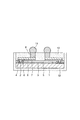
図1はこの発明の一実施形態としての半導体装置の断面図を示す。この半導体装置は、一般的にはCSP(chip size package)と呼ばれるものであり、シリコン基板(半導体基板)1を備えている。シリコン基板1の上面には所定の機能の集積回路(図示せず)が設けられ、上面周辺部にはアルミニウム系金属等からなる複数の接続パッド2が集積回路に接続されて設けられている。
FIG. 1 is a sectional view of a semiconductor device as an embodiment of the present invention. This semiconductor device is generally called a CSP (chip size package) and includes a silicon substrate (semiconductor substrate) 1. An integrated circuit (not shown) having a predetermined function is provided on the upper surface of the
接続パッド2の中央部を除くシリコン基板1の上面には酸化シリコンや窒化シリコン等からなる絶縁膜3が設けられ、接続パッド2の中央部は絶縁膜3に設けられた開口部4を介して露出されている。絶縁膜3の上面にはエポキシ系樹脂やポリイミド系樹脂等からなる保護膜(絶縁膜)5が設けられている。この場合、絶縁膜3の開口部4に対応する部分における保護膜5には開口部6が設けられている。
An
保護膜5の上面には銅等からなる下地金属層7が設けられている。下地金属層7の上面全体には銅からなる配線8が設けられている。下地金属層7を含む配線8の一端部は、絶縁膜3及び保護膜5の開口部4、6を介して接続パッド2に接続されている。配線8の接続パッド部上面には高さ80〜150μmの銅からなる柱状電極9が設けられている。
A
配線8を含む保護膜5の上面には、後述する第1の封止材料からなる第1の封止膜10がその上面が柱状電極9の上面と面一となるように設けられている。柱状電極9の上面には半田ボール11が設けられている。シリコン基板1、絶縁膜3、保護膜5及び第1の封止膜10の周側面とシリコン基板1の下面には、後述する第2の封止材料からなる第2の封止膜12が設けられている。
A
次に、第1、第2の封止膜10、12の材料について説明する。第1、第2の封止膜10、12の材料は、エポキシ系樹脂、ポリイミド系樹脂、アクリル系樹脂、シリコーン系樹脂、ゴム系樹脂、ビスマレイミド系樹脂等の有機材料のいずれであってもよいが、第1、第2の封止膜10、12にそれぞれ要求される特性がやや異なるため、それに適した材料であることが望ましい。
Next, materials of the first and
すなわち、第1の封止膜10は、塵埃、湿気、機械的破損等の環境に対する保護効果を増大するためのものであるが、配線8及び柱状電極9の腐食あるいはそれらの間でのショートが発生しないようにする必要がある。このため、第1の封止膜10を形成するための第1の封止材料としては、Naイオン、Kイオン、CaイオンおよびClイオンの各不純物濃度を10ppm以下とかなり低くした比較的高価なものを用いる。また、半導体装置の製造において、半導体層や接続パッド2を含む導電層と共にクリーンルーム内で形成される絶縁膜3および保護膜5中のNaイオン、Kイオン、CaイオンおよびClイオンの各不純物濃度は、10ppm以下である。
In other words, the
一方、第2の封止膜12は、特に機械的破損に対する保護効果を増大するためのものであるが、下地金属層7を含む配線8及び柱状電極9の腐食あるいはそれらの間でのショートが発生しないようにする必要性はあまりない。このため、第2の封止膜12を形成するための第2の封止材料としては、Naイオン、Kイオン、CaイオンおよびClイオンの合計不純物濃度が多少高くてもよく、この合計不純物濃度を100ppm以上とある程度高くした比較的安価なものを用いる。
On the other hand, the
また、第1、第2の封止膜10、12とシリコン基板1との間の熱膨張係数差に起因する応力を緩和するために、第1、第2の封止材料中にシリカフィラー等を混入することが一般的に行なわれているが、この場合も、第1、第2の封止膜10、12にそれぞれ要求される特性がやや異なるため、それに適した混入量であることが望ましい。
Moreover, in order to relieve the stress caused by the difference in thermal expansion coefficient between the first and
すなわち、第1の封止膜10は、配線8及び柱状電極9を含むシリコン基板1上を覆うものであるため、高い信頼性が要求され、シリコン基板1との熱膨張係数差が小さい方が望ましい。このため、第1の封止膜10を形成するための第1の封止材料としては、シリカフィラー等の混入量を比較的多くして熱膨張係数をシリコン基板1の熱膨張係数(3.5ppm/℃)に近づけ、熱膨張係数20ppm/℃未満としたものを用いる。
That is, since the
一方、第2の封止膜12は、シリコン基板1、絶縁膜3、保護膜5及び第1の封止膜10の周側面とシリコン基板1の下面を覆うものであるため、第1の封止膜10ほどの高い信頼性を必要とせず、シリカフィラー等の混入により硬くなりすぎてクラックが発生しやすくなるのを避けるために、第1の封止膜10よりもある程度軟らかいものの方が望ましい。このため、第2の封止膜12を形成するための第2の封止材料としては、シリカフィラー等の混入量を比較的少なくし、熱膨張係数20ppm/℃以上としたものを用いる。
On the other hand, the
以上の結果、第1の封止膜10は、イオン不純物濃度10ppm以下で熱膨張係数20ppm/℃未満の比較的高価な第1の封止材料によって形成されている。第2の封止膜12は、イオン不純物濃度100ppm以上で熱膨張係数20ppm/℃以上の比較的安価な第2の封止材料によって形成されている。したがって、比較的高価な第1の封止材料のみを用いる場合と比較して、比較的安価な第2の封止材料を用いる分だけ、封止材料費を低減することができる。
As a result, the
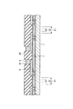
(製造方法の第1の例)
次に、図1に示す半導体装置の製造方法の第1の例について説明する。まず、図2に示すように、ウエハ状態のシリコン基板1上にアルミニウム系金属等からなる接続パッド2、酸化シリコンや窒化シリコン等からなる絶縁膜3及びエポキシ系樹脂やポリイミド系樹脂等からなる保護膜5が設けられ、接続パッド2の中央部が絶縁膜3及び保護膜5に形成された開口部4、6を介して露出されたものを用意する。
(First example of manufacturing method)
Next, a first example of the method for manufacturing the semiconductor device shown in FIG. 1 will be described. First, as shown in FIG. 2, a
上記において、ウエハ状態のシリコン基板1には、各半導体装置が形成される領域に所定の機能の集積回路が形成され、接続パッド2は、それぞれ、対応する領域に形成された集積回路に電気的に接続されている。なお、図2において、符号21で示す領域は第1のダイシングストリートに対応する領域であり、符号22で示す領域は第2のダイシングストリートに対応する領域である。この場合、第2のダイシングストリート22は、第1のダイシングストリート21の幅方向中央部に対応する領域となっている。
In the above, on the
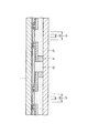
次に、図3に示すように、絶縁膜3及び保護膜5の開口部4、6を介して露出された接続パッド2の上面を含む保護膜5の上面全体に下地金属層7を形成する。この場合、下地金属層7は、無電解メッキにより形成された銅層のみであってもよく、またスパッタにより形成された銅層のみであってもよく、さらにスパッタにより形成されたチタン等の薄膜層上にスパッタにより銅層を形成したものであってもよい。
Next, as shown in FIG. 3, a
次に、下地金属層7の上面にメッキレジスト膜23をパターン形成する。この場合、配線8形成領域に対応する部分におけるメッキレジスト膜23には開口部24が形成されている。次に、下地金属層7をメッキ電流路として銅の電解メッキを行なうことにより、メッキレジスト膜23の開口部24内の下地金属層7の上面に配線8を形成する。次に、メッキレジスト膜23を剥離する。
Next, a plating resist
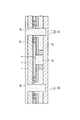
次に、図4に示すように、配線8を含む下地金属層7の上面にメッキレジスト膜25をパターン形成する。この場合、柱状電極9形成領域に対応する部分におけるメッキレジスト膜25には開口部26が形成されている。次に、下地金属層7をメッキ電流路として銅の電解メッキを行なうことにより、メッキレジスト膜25の開口部26内の配線8の接続パッド部上面に柱状電極9を形成する。次に、メッキレジスト膜25を剥離し、次いで、配線8をマスクとして下地金属層7の不要な部分をエッチングして除去すると、図5に示すように、配線8下にのみ下地金属層7が残存される。
Next, as shown in FIG. 4, a plating resist
次に、図6に示すように、スクリーン印刷法、スピンコート法、ダイコート法等により、柱状電極9及び配線8を含む保護膜5の上面全体に第1の封止材料からなる第1の封止膜10をその厚さが柱状電極9の高さよりも厚くなるように形成する。したがって、この状態では、柱状電極9の上面は第1の封止膜10によって覆われている。
Next, as shown in FIG. 6, the first sealing material made of the first sealing material is formed on the entire upper surface of the
次に、第1の封止膜10及び柱状電極9の上面側を適宜に研磨し、図7に示すように、柱状電極9の上面を露出させ、且つ、この露出された柱状電極9の上面を含む第1の封止膜10の上面を平坦化する。ここで、柱状電極9の上面側を適宜に研磨するのは、電解メッキにより形成される柱状電極9の高さにばらつきがあるため、このばらつきを解消して、柱状電極9の高さを均一にするためである。
Next, the upper surface side of the
次に、図7に示すものの上下を反転し、図8に示すように、柱状電極9の下面を含む第1の封止膜10の下面を第1のダイシングフィルム27の上面に貼り付ける。次に、図9に示すように、第1のダイシングストリート21に沿って、ダイシング法やレーザーカット法等により、シリコン基板1、絶縁膜3、保護膜5及び第1の封止膜10をフルカットする。この場合、第1のダイシングフィルム27の厚さ方向中間までカットする。すると、ウエハ状態のシリコン基板1は個々のチップに分離されるが、各チップが第1のダイシングフィルム27に貼り付けられているので、第1のダイシングフィルム27の上面を含む各チップ間つまり第1のダイシングストリート21に対応する領域には溝28が形成されている。
7 is turned upside down, and the lower surface of the
次に、図10に示すように、スクリーン印刷法、スピンコート法、ダイコート法等により、溝28内を含むシリコン基板1の上面全体に第2の封止材料からなる第2の封止膜12をその上面が平坦となるように形成する。この状態では、シリコン基板1、絶縁膜3、保護膜5及び第1の封止膜10の周側面は、溝28内に形成された第2の封止膜12によって覆われている。また、シリコン基板1は個々のチップに分離されているので、シリコン基板1が反りにくいようにすることができる。なお、第1のダイシングフィルム27をその周囲方向に引っ張って拡張し、これにより溝28の幅を広げ、この状態で溝28内に第2の封止材料を塗布すると、溝28内に第2の封止材料を充填しやすくすることができる。
Next, as shown in FIG. 10, the
次に、図10に示すものの上下を反転し、次いで、第1のダイシングフィルム27を剥離すると、図11に示すようになる。この状態では、各チップ間及び各シリコン基板1の下面に第2の封止膜12が形成されているので、各チップは一体化されている。また、符号12aで示すように、図10に示す第1のダイシングフィルム27に形成された溝28内に形成された第2の封止膜12が第1の封止膜10の上面から突出されている。次に、この突出部12aを研磨して除去すると、図12に示すようになる。
Next, when the one shown in FIG. 10 is turned upside down and then the
次に、図13に示すように、柱状電極9の上面に半田ボール11を形成する。次に、第2の封止膜12の下面を第2のダイシングフィルム29の上面に貼り付ける。次に、図14に示すように、第2のダイシングストリート22に沿って、ダイシング法やレーザーカット法等により、溝28内に形成された第2の封止膜12の幅方向中央部をフルカットする。次に、第1、第2の封止膜12等を含むシリコン基板1を第2のダイシングフィルム29から剥離すると、図1に示す半導体装置が複数個得られる。
Next, as shown in FIG. 13,
(製造方法の第2の例)
次に、図1に示す半導体装置の製造方法の第2の例について説明する。この場合、図10に示す工程後に、図15に示すように、第2のダイシングストリート22に沿って、ダイシング法やレーザーカット法等により、溝28内に形成された第2の封止膜12の幅方向中央部をフルカットし、溝31を形成する。この状態では、第2の封止膜12等を含むシリコン基板1は溝31により個々のチップに分離されるが、第1のダイシングフィルム27に貼り付けられているので、ばらばらとなることはない。
(Second example of manufacturing method)
Next, a second example of the method for manufacturing the semiconductor device shown in FIG. 1 will be described. In this case, after the step shown in FIG. 10, as shown in FIG. 15, the
次に、図16に示すように、第2の封止膜12の上面にサポートフィルム32を貼り付ける。次に、図16に示すものの上下を反転し、次いで、第1のダイシングフィルム27を剥離すると、図17に示すようになる。この状態では、符号12bで示すように、図15に示す第1のダイシングフィルム27に形成された溝28内に形成された第2の封止膜12が第1の封止膜10の上面から突出されている。次に、この突出部12bを研磨して除去すると、図18に示すようになる。
Next, as shown in FIG. 16, a
次に、図19に示すように、柱状電極9の上面に半田ボール11を形成する。この状態では、第1、第2の封止膜10、12等を含むシリコン基板1は、サポートフィルム32に貼り付けられているが、溝31により個々のチップに分離されている。そこで、次に、第1、第2の封止膜10、12等を含むシリコン基板1をサポートフィルム32から剥離すると、図1に示す半導体装置が複数個得られる。
Next, as shown in FIG. 19,
(製造方法の第3の例)
次に、図1に示す半導体装置の製造方法の第3の例について説明する。この場合、図7に示す工程後に、図20に示すように、シリコン基板1の下面を第1のダイシングフィルム41の上面に貼り付ける。次に、図21に示すように、第1のダイシングストリート21に沿って、ダイシング法やレーザーカット法等により、第1の封止膜10、保護膜5、絶縁膜3及びシリコン基板1をフルカットする。この場合も、ダイシングフィルム41の厚さ方向中間までカットする。すると、ウエハ状態のシリコン基板1は個々のチップに分離されるが、各チップが第1のダイシングフィルム41に貼り付けられているので、第1のダイシングフィルム41の上面を含む各チップ間つまり第1のダイシングストリート21に対応する領域には溝42が形成されている。
(Third example of manufacturing method)
Next, a third example of the method for manufacturing the semiconductor device shown in FIG. 1 will be described. In this case, after the step shown in FIG. 7, the lower surface of the
次に、図22に示すように、柱状電極9の上面を含む第1の封止膜10の上面に第2のダイシングフィルム43を貼り付ける。次に、図22に示すものの上下を反転し、次いで、第1のダイシングフィルム41を剥離すると、図23に示すようになる。次に、図24に示すように、スクリーン印刷法、スピンコート法、ダイコート法等により、溝42内を含むシリコン基板1の上面全体に第2の封止材料からなる第2の封止膜12をその上面が平坦となるように形成する。
Next, as shown in FIG. 22, a
この状態では、シリコン基板1、絶縁膜3、保護膜5及び第1の封止膜10の周側面は、溝42内に形成された第2の封止膜12によって覆われている。また、シリコン基板1は個々のチップに分離されているので、シリコン基板1が反りにくいようにすることができる。なお、第2のダイシングフィルム43をその周囲方向に引っ張って拡張し、これにより溝42の幅を広げ、この状態で溝42内に第2の封止材料を塗布すると、溝42内に第2の封止材料を充填しやすくすることができる。
In this state, the peripheral side surfaces of the
次に、図25に示すように、第2のダイシングストリート22に沿って、ダイシング法やレーザーカット法等により、溝42内に形成された第2の封止膜12の幅方向中央部をフルカットする。次に、図25に示すものの上下を反転し、次いで、図26に示すように、第2の封止膜12の下面をサポートフィルム44の上面に貼り付ける。次に、ダイシングフィルム43を剥離すると、図18に示す場合と同じとなる。以下の工程は、上記製造方法の第2の例の場合と同じであるので、その説明を省略する。ところで、この製造方法の場合には、例えば、図17に示すような突出部12bが形成されないため、このような突出部12bを除去するための研磨工程は不要となる。
Next, as shown in FIG. 25, the center in the width direction of the
1 シリコン基板
2 接続パッド
3 絶縁膜
5 保護膜
7 下地金属層
8 配線
9 柱状電極
10 第1の封止膜
11 半田ボール
12 第2の封止膜
21、22 ダイシングストリート
27、29 ダイシングフィルム
DESCRIPTION OF
Claims (8)
Priority Applications (5)
| Application Number | Priority Date | Filing Date | Title |
|---|---|---|---|
| JP2005100737A JP4003780B2 (en) | 2004-09-17 | 2005-03-31 | Semiconductor device and manufacturing method thereof |
| US11/226,769 US7417330B2 (en) | 2004-09-17 | 2005-09-14 | Semiconductor device packaged into chip size and manufacturing method thereof |
| TW094131762A TW200614404A (en) | 2004-09-17 | 2005-09-15 | Semiconductor device and manufacturing method thereof |
| KR1020050086569A KR100727519B1 (en) | 2004-09-17 | 2005-09-16 | Semiconductor device packaged into chip size and manufacturing method thereof |
| US12/218,685 US7867826B2 (en) | 2004-09-17 | 2008-07-17 | Semiconductor device packaged into chip size and manufacturing method thereof |
Applications Claiming Priority (2)
| Application Number | Priority Date | Filing Date | Title |
|---|---|---|---|
| JP2004270646 | 2004-09-17 | ||
| JP2005100737A JP4003780B2 (en) | 2004-09-17 | 2005-03-31 | Semiconductor device and manufacturing method thereof |
Publications (2)
| Publication Number | Publication Date |
|---|---|
| JP2006114867A JP2006114867A (en) | 2006-04-27 |
| JP4003780B2 true JP4003780B2 (en) | 2007-11-07 |
Family
ID=36073083
Family Applications (1)
| Application Number | Title | Priority Date | Filing Date |
|---|---|---|---|
| JP2005100737A Expired - Fee Related JP4003780B2 (en) | 2004-09-17 | 2005-03-31 | Semiconductor device and manufacturing method thereof |
Country Status (4)
| Country | Link |
|---|---|
| US (2) | US7417330B2 (en) |
| JP (1) | JP4003780B2 (en) |
| KR (1) | KR100727519B1 (en) |
| TW (1) | TW200614404A (en) |
Families Citing this family (66)
| Publication number | Priority date | Publication date | Assignee | Title |
|---|---|---|---|---|
| JP4193897B2 (en) | 2006-05-19 | 2008-12-10 | カシオ計算機株式会社 | Semiconductor device and manufacturing method thereof |
| JP4812525B2 (en) * | 2006-06-12 | 2011-11-09 | パナソニック株式会社 | Semiconductor device, semiconductor device mounting body, and semiconductor device manufacturing method |
| JP5119756B2 (en) * | 2006-06-30 | 2013-01-16 | 株式会社デンソー | Wiring board |
| JP2008098529A (en) * | 2006-10-13 | 2008-04-24 | Toshiba Corp | Semiconductor device, and manufacturing method thereof |
| US8749065B2 (en) * | 2007-01-25 | 2014-06-10 | Tera Probe, Inc. | Semiconductor device comprising electromigration prevention film and manufacturing method thereof |
| JP2008227398A (en) * | 2007-03-15 | 2008-09-25 | Sanken Electric Co Ltd | Method of manufacturing semiconductor device |
| TWI341577B (en) * | 2007-03-27 | 2011-05-01 | Unimicron Technology Corp | Semiconductor chip embedding structure |
| US8445325B2 (en) | 2007-05-04 | 2013-05-21 | Stats Chippac, Ltd. | Package-in-package using through-hole via die on saw streets |
| US7723159B2 (en) * | 2007-05-04 | 2010-05-25 | Stats Chippac, Ltd. | Package-on-package using through-hole via die on saw streets |
| US7829998B2 (en) | 2007-05-04 | 2010-11-09 | Stats Chippac, Ltd. | Semiconductor wafer having through-hole vias on saw streets with backside redistribution layer |
| US7838424B2 (en) * | 2007-07-03 | 2010-11-23 | Taiwan Semiconductor Manufacturing Company, Ltd. | Enhanced reliability of wafer-level chip-scale packaging (WLCSP) die separation using dry etching |
| JP2009049218A (en) * | 2007-08-21 | 2009-03-05 | Nec Electronics Corp | Semiconductor device, and manufacturing method of semiconductor device |
| US8587124B2 (en) * | 2007-09-21 | 2013-11-19 | Teramikros, Inc. | Semiconductor device having low dielectric insulating film and manufacturing method of the same |
| US20090079072A1 (en) * | 2007-09-21 | 2009-03-26 | Casio Computer Co., Ltd. | Semiconductor device having low dielectric insulating film and manufacturing method of the same |
| JP2009146988A (en) * | 2007-12-12 | 2009-07-02 | Fujitsu Ltd | Method of singulating circuit board and package circuit board |
| JP4666028B2 (en) * | 2008-03-31 | 2011-04-06 | カシオ計算機株式会社 | Semiconductor device |
| JP4538764B2 (en) * | 2008-07-24 | 2010-09-08 | カシオ計算機株式会社 | Semiconductor device and manufacturing method thereof |
| US9235876B2 (en) | 2009-03-02 | 2016-01-12 | Flir Systems, Inc. | Row and column noise reduction in thermal images |
| US10757308B2 (en) | 2009-03-02 | 2020-08-25 | Flir Systems, Inc. | Techniques for device attachment with dual band imaging sensor |
| USD765081S1 (en) | 2012-05-25 | 2016-08-30 | Flir Systems, Inc. | Mobile communications device attachment with camera |
| US9986175B2 (en) | 2009-03-02 | 2018-05-29 | Flir Systems, Inc. | Device attachment with infrared imaging sensor |
| US10244190B2 (en) | 2009-03-02 | 2019-03-26 | Flir Systems, Inc. | Compact multi-spectrum imaging with fusion |
| US9517679B2 (en) | 2009-03-02 | 2016-12-13 | Flir Systems, Inc. | Systems and methods for monitoring vehicle occupants |
| US9756264B2 (en) | 2009-03-02 | 2017-09-05 | Flir Systems, Inc. | Anomalous pixel detection |
| US9948872B2 (en) | 2009-03-02 | 2018-04-17 | Flir Systems, Inc. | Monitor and control systems and methods for occupant safety and energy efficiency of structures |
| US9635285B2 (en) | 2009-03-02 | 2017-04-25 | Flir Systems, Inc. | Infrared imaging enhancement with fusion |
| WO2012170949A2 (en) | 2011-06-10 | 2012-12-13 | Flir Systems, Inc. | Non-uniformity correction techniques for infrared imaging devices |
| US9208542B2 (en) | 2009-03-02 | 2015-12-08 | Flir Systems, Inc. | Pixel-wise noise reduction in thermal images |
| US9473681B2 (en) | 2011-06-10 | 2016-10-18 | Flir Systems, Inc. | Infrared camera system housing with metalized surface |
| US9843742B2 (en) | 2009-03-02 | 2017-12-12 | Flir Systems, Inc. | Thermal image frame capture using de-aligned sensor array |
| US9998697B2 (en) | 2009-03-02 | 2018-06-12 | Flir Systems, Inc. | Systems and methods for monitoring vehicle occupants |
| US9451183B2 (en) | 2009-03-02 | 2016-09-20 | Flir Systems, Inc. | Time spaced infrared image enhancement |
| US9674458B2 (en) | 2009-06-03 | 2017-06-06 | Flir Systems, Inc. | Smart surveillance camera systems and methods |
| US10091439B2 (en) | 2009-06-03 | 2018-10-02 | Flir Systems, Inc. | Imager with array of multiple infrared imaging modules |
| US9292909B2 (en) | 2009-06-03 | 2016-03-22 | Flir Systems, Inc. | Selective image correction for infrared imaging devices |
| US9843743B2 (en) | 2009-06-03 | 2017-12-12 | Flir Systems, Inc. | Infant monitoring systems and methods using thermal imaging |
| US9756262B2 (en) | 2009-06-03 | 2017-09-05 | Flir Systems, Inc. | Systems and methods for monitoring power systems |
| US9716843B2 (en) | 2009-06-03 | 2017-07-25 | Flir Systems, Inc. | Measurement device for electrical installations and related methods |
| US9819880B2 (en) | 2009-06-03 | 2017-11-14 | Flir Systems, Inc. | Systems and methods of suppressing sky regions in images |
| US9207708B2 (en) | 2010-04-23 | 2015-12-08 | Flir Systems, Inc. | Abnormal clock rate detection in imaging sensor arrays |
| US9706138B2 (en) | 2010-04-23 | 2017-07-11 | Flir Systems, Inc. | Hybrid infrared sensor array having heterogeneous infrared sensors |
| US9918023B2 (en) | 2010-04-23 | 2018-03-13 | Flir Systems, Inc. | Segmented focal plane array architecture |
| US9848134B2 (en) | 2010-04-23 | 2017-12-19 | Flir Systems, Inc. | Infrared imager with integrated metal layers |
| JP2012009816A (en) * | 2010-05-28 | 2012-01-12 | Casio Comput Co Ltd | Semiconductor device and method of manufacturing the same |
| JP2012039005A (en) * | 2010-08-10 | 2012-02-23 | Toshiba Corp | Semiconductor device and method of manufacturing the same |
| US10389953B2 (en) | 2011-06-10 | 2019-08-20 | Flir Systems, Inc. | Infrared imaging device having a shutter |
| KR101808375B1 (en) | 2011-06-10 | 2017-12-12 | 플리어 시스템즈, 인크. | Low power and small form factor infrared imaging |
| EP2719166B1 (en) | 2011-06-10 | 2018-03-28 | Flir Systems, Inc. | Line based image processing and flexible memory system |
| US9706137B2 (en) | 2011-06-10 | 2017-07-11 | Flir Systems, Inc. | Electrical cabinet infrared monitor |
| US10169666B2 (en) | 2011-06-10 | 2019-01-01 | Flir Systems, Inc. | Image-assisted remote control vehicle systems and methods |
| US9961277B2 (en) | 2011-06-10 | 2018-05-01 | Flir Systems, Inc. | Infrared focal plane array heat spreaders |
| US9900526B2 (en) | 2011-06-10 | 2018-02-20 | Flir Systems, Inc. | Techniques to compensate for calibration drifts in infrared imaging devices |
| US10841508B2 (en) | 2011-06-10 | 2020-11-17 | Flir Systems, Inc. | Electrical cabinet infrared monitor systems and methods |
| US9143703B2 (en) | 2011-06-10 | 2015-09-22 | Flir Systems, Inc. | Infrared camera calibration techniques |
| US10079982B2 (en) | 2011-06-10 | 2018-09-18 | Flir Systems, Inc. | Determination of an absolute radiometric value using blocked infrared sensors |
| US10051210B2 (en) | 2011-06-10 | 2018-08-14 | Flir Systems, Inc. | Infrared detector array with selectable pixel binning systems and methods |
| US9235023B2 (en) | 2011-06-10 | 2016-01-12 | Flir Systems, Inc. | Variable lens sleeve spacer |
| US9509924B2 (en) | 2011-06-10 | 2016-11-29 | Flir Systems, Inc. | Wearable apparatus with integrated infrared imaging module |
| US9058653B1 (en) | 2011-06-10 | 2015-06-16 | Flir Systems, Inc. | Alignment of visible light sources based on thermal images |
| US9635220B2 (en) | 2012-07-16 | 2017-04-25 | Flir Systems, Inc. | Methods and systems for suppressing noise in images |
| US9811884B2 (en) | 2012-07-16 | 2017-11-07 | Flir Systems, Inc. | Methods and systems for suppressing atmospheric turbulence in images |
| KR101790090B1 (en) * | 2013-05-02 | 2017-10-25 | 후지필름 가부시키가이샤 | Etching method, etching liquid and etching liquid kit to be used in said method, and semiconductor substrate product manufacturing method |
| US9973692B2 (en) | 2013-10-03 | 2018-05-15 | Flir Systems, Inc. | Situational awareness by compressed display of panoramic views |
| US11297264B2 (en) | 2014-01-05 | 2022-04-05 | Teledyne Fur, Llc | Device attachment with dual band imaging sensor |
| US20180096909A1 (en) * | 2016-10-05 | 2018-04-05 | Nxp B.V. | Semiconductor device having two encapsulants |
| US10522440B2 (en) * | 2017-11-07 | 2019-12-31 | Taiwan Semiconductor Manufacturing Co., Ltd. | Package structure and method of manufacturing the same |
Family Cites Families (26)
| Publication number | Priority date | Publication date | Assignee | Title |
|---|---|---|---|---|
| JPS57113235A (en) * | 1980-12-29 | 1982-07-14 | Nec Corp | Semiconductor device |
| JPH07100766B2 (en) * | 1987-06-25 | 1995-11-01 | ソマール株式会社 | Epoxy resin powder coating composition |
| JP2643714B2 (en) * | 1992-02-07 | 1997-08-20 | 信越化学工業株式会社 | Liquid epoxy resin composition and cured product |
| JP3388369B2 (en) | 1994-01-31 | 2003-03-17 | 日本テキサス・インスツルメンツ株式会社 | Semiconductor package equipment |
| JPH08335653A (en) * | 1995-04-07 | 1996-12-17 | Nitto Denko Corp | Semiconductor device, its production and tape carrier for semiconductor device used for production of the semiconductor device |
| JPH1095910A (en) * | 1996-09-26 | 1998-04-14 | Fuji Electric Co Ltd | Unsaturated polyester resin composition for semiconductor sealing use and molding thereof |
| JP3671563B2 (en) * | 1996-12-09 | 2005-07-13 | 株式会社デンソー | Semiconductor device having a structure in which a mold IC is fixed to a case |
| JP3658160B2 (en) * | 1997-11-17 | 2005-06-08 | キヤノン株式会社 | Molding machine |
| JP3291289B2 (en) * | 2000-01-19 | 2002-06-10 | サンユレック株式会社 | Electronic component manufacturing method |
| US6744124B1 (en) | 1999-12-10 | 2004-06-01 | Siliconix Incorporated | Semiconductor die package including cup-shaped leadframe |
| JP3955712B2 (en) | 2000-03-03 | 2007-08-08 | 株式会社ルネサステクノロジ | Semiconductor device |
| JP3455948B2 (en) | 2000-05-19 | 2003-10-14 | カシオ計算機株式会社 | Semiconductor device and manufacturing method thereof |
| US6391687B1 (en) | 2000-10-31 | 2002-05-21 | Fairchild Semiconductor Corporation | Column ball grid array package |
| JP2003060130A (en) * | 2001-08-08 | 2003-02-28 | Seiko Epson Corp | Semiconductor device, sealing method therefor and mounting method using the device |
| US6620651B2 (en) | 2001-10-23 | 2003-09-16 | National Starch And Chemical Investment Holding Corporation | Adhesive wafers for die attach application |
| JP2003174111A (en) | 2001-12-06 | 2003-06-20 | Sanyo Electric Co Ltd | Semiconductor device |
| JP2003197802A (en) | 2001-12-25 | 2003-07-11 | Kyocera Corp | Vessel for receiving electronic component |
| JP2003273279A (en) * | 2002-03-18 | 2003-09-26 | Mitsubishi Electric Corp | Semiconductor device and its manufacturing method |
| JP2003309228A (en) * | 2002-04-18 | 2003-10-31 | Oki Electric Ind Co Ltd | Semiconductor device and manufacturing method therefor |
| JP4243075B2 (en) * | 2002-06-13 | 2009-03-25 | パナソニック株式会社 | Semiconductor device and manufacturing method thereof |
| US6770971B2 (en) * | 2002-06-14 | 2004-08-03 | Casio Computer Co., Ltd. | Semiconductor device and method of fabricating the same |
| JP2004221417A (en) * | 2003-01-16 | 2004-08-05 | Casio Comput Co Ltd | Semiconductor device and its producing method |
| KR100495007B1 (en) * | 2003-02-17 | 2005-06-14 | 삼성전자주식회사 | Wafer level vacuum packaging method using Si wafer |
| US6777263B1 (en) * | 2003-08-21 | 2004-08-17 | Agilent Technologies, Inc. | Film deposition to enhance sealing yield of microcap wafer-level package with vias |
| JP3915992B2 (en) * | 2004-06-08 | 2007-05-16 | ローム株式会社 | Manufacturing method of surface mount type electronic components |
| JP4271625B2 (en) * | 2004-06-30 | 2009-06-03 | 株式会社フジクラ | Semiconductor package and manufacturing method thereof |
-
2005
- 2005-03-31 JP JP2005100737A patent/JP4003780B2/en not_active Expired - Fee Related
- 2005-09-14 US US11/226,769 patent/US7417330B2/en not_active Expired - Fee Related
- 2005-09-15 TW TW094131762A patent/TW200614404A/en unknown
- 2005-09-16 KR KR1020050086569A patent/KR100727519B1/en not_active IP Right Cessation
-
2008
- 2008-07-17 US US12/218,685 patent/US7867826B2/en not_active Expired - Fee Related
Also Published As
| Publication number | Publication date |
|---|---|
| KR20060051364A (en) | 2006-05-19 |
| TW200614404A (en) | 2006-05-01 |
| US7867826B2 (en) | 2011-01-11 |
| US7417330B2 (en) | 2008-08-26 |
| TWI296139B (en) | 2008-04-21 |
| US20080286903A1 (en) | 2008-11-20 |
| JP2006114867A (en) | 2006-04-27 |
| KR100727519B1 (en) | 2007-06-14 |
| US20060060984A1 (en) | 2006-03-23 |
Similar Documents
| Publication | Publication Date | Title |
|---|---|---|
| JP4003780B2 (en) | Semiconductor device and manufacturing method thereof | |
| JP5183708B2 (en) | Semiconductor device and manufacturing method thereof | |
| KR100659625B1 (en) | Semiconductor device and method for manufacturing the same | |
| KR100589570B1 (en) | Method for manufacturing semiconductor device | |
| JP2009181981A (en) | Manufacturing process of semiconductor device, and the semiconductor device | |
| US20060141750A1 (en) | Semiconductor integrated device and method for manufacturing same | |
| JP2006229113A (en) | Semiconductor device and its fabrication process | |
| TW201542049A (en) | Substrate with electrical interconnector structure and manufacturing method thereof | |
| JP2002231854A (en) | Semiconductor device and its manufacturing method | |
| JP2010225648A (en) | Semiconductor device and method of manufacturing the same | |
| JP2008130886A (en) | Manufacturing method of semiconductor device | |
| JP2006173548A (en) | Semiconductor apparatus and manufacturing method thereof | |
| JP4913563B2 (en) | Manufacturing method of semiconductor device | |
| JP4492621B2 (en) | Semiconductor device and manufacturing method thereof | |
| CN109192706B (en) | Chip packaging structure and chip packaging method | |
| JP2008244383A (en) | Semiconductor device and its manufacturing method | |
| JP5004907B2 (en) | Manufacturing method of semiconductor device | |
| JP2008218494A (en) | Semiconductor device and its manufacturing method | |
| JP2005183518A (en) | Semiconductor device and its manufacturing method, circuit board and electronic equipment | |
| JP2007281289A (en) | Electronic component and manufacturing method thereof | |
| JP4986417B2 (en) | Semiconductor device and manufacturing method of semiconductor device | |
| JP2005183868A (en) | Semiconductor device and its packaging structure | |
| JP2013065582A (en) | Semiconductor wafer, semiconductor device and semiconductor device manufacturing method | |
| JP5095991B2 (en) | Manufacturing method of semiconductor device | |
| JP2008283216A (en) | Semiconductor device, and manufacturing method thereof |
Legal Events
| Date | Code | Title | Description |
|---|---|---|---|
| RD02 | Notification of acceptance of power of attorney |
Free format text: JAPANESE INTERMEDIATE CODE: A7422 Effective date: 20060213 |
|
| RD04 | Notification of resignation of power of attorney |
Free format text: JAPANESE INTERMEDIATE CODE: A7424 Effective date: 20060310 |
|
| A977 | Report on retrieval |
Free format text: JAPANESE INTERMEDIATE CODE: A971007 Effective date: 20070720 |
|
| TRDD | Decision of grant or rejection written | ||
| A01 | Written decision to grant a patent or to grant a registration (utility model) |
Free format text: JAPANESE INTERMEDIATE CODE: A01 Effective date: 20070731 |
|
| A61 | First payment of annual fees (during grant procedure) |
Free format text: JAPANESE INTERMEDIATE CODE: A61 Effective date: 20070813 |
|
| R150 | Certificate of patent or registration of utility model |
Free format text: JAPANESE INTERMEDIATE CODE: R150 |
|
| FPAY | Renewal fee payment (event date is renewal date of database) |
Free format text: PAYMENT UNTIL: 20100831 Year of fee payment: 3 |
|
| FPAY | Renewal fee payment (event date is renewal date of database) |
Free format text: PAYMENT UNTIL: 20100831 Year of fee payment: 3 |
|
| FPAY | Renewal fee payment (event date is renewal date of database) |
Free format text: PAYMENT UNTIL: 20110831 Year of fee payment: 4 |
|
| FPAY | Renewal fee payment (event date is renewal date of database) |
Free format text: PAYMENT UNTIL: 20120831 Year of fee payment: 5 |
|
| FPAY | Renewal fee payment (event date is renewal date of database) |
Free format text: PAYMENT UNTIL: 20120831 Year of fee payment: 5 |
|
| FPAY | Renewal fee payment (event date is renewal date of database) |
Free format text: PAYMENT UNTIL: 20120831 Year of fee payment: 5 |
|
| S111 | Request for change of ownership or part of ownership |
Free format text: JAPANESE INTERMEDIATE CODE: R313111 |
|
| FPAY | Renewal fee payment (event date is renewal date of database) |
Free format text: PAYMENT UNTIL: 20120831 Year of fee payment: 5 |
|
| R350 | Written notification of registration of transfer |
Free format text: JAPANESE INTERMEDIATE CODE: R350 |
|
| FPAY | Renewal fee payment (event date is renewal date of database) |
Free format text: PAYMENT UNTIL: 20120831 Year of fee payment: 5 |
|
| FPAY | Renewal fee payment (event date is renewal date of database) |
Free format text: PAYMENT UNTIL: 20130831 Year of fee payment: 6 |
|
| R250 | Receipt of annual fees |
Free format text: JAPANESE INTERMEDIATE CODE: R250 |
|
| R250 | Receipt of annual fees |
Free format text: JAPANESE INTERMEDIATE CODE: R250 |
|
| LAPS | Cancellation because of no payment of annual fees |