JP4001453B2 - Droplet discharge head, method for manufacturing the same, image forming apparatus, and droplet discharge apparatus - Google Patents
Droplet discharge head, method for manufacturing the same, image forming apparatus, and droplet discharge apparatus Download PDFInfo
- Publication number
- JP4001453B2 JP4001453B2 JP2000219803A JP2000219803A JP4001453B2 JP 4001453 B2 JP4001453 B2 JP 4001453B2 JP 2000219803 A JP2000219803 A JP 2000219803A JP 2000219803 A JP2000219803 A JP 2000219803A JP 4001453 B2 JP4001453 B2 JP 4001453B2
- Authority
- JP
- Japan
- Prior art keywords
- droplet discharge
- diaphragm
- discharge head
- liquid chamber
- concentration
- Prior art date
- Legal status (The legal status is an assumption and is not a legal conclusion. Google has not performed a legal analysis and makes no representation as to the accuracy of the status listed.)
- Expired - Fee Related
Links
Images


Description
【0001】
【産業上の利用分野】
本発明は液滴吐出ヘッド及びその製造方法、画像形成装置、液滴吐出装置に関する
【0002】
【従来の技術】
プリンタ、ファクシミリ、複写装置等の画像記録装置或いは画像形成装置として用いるインクジェット記録装置において使用する液滴吐出ヘッドであるインクジェットヘッドとしては、インク滴を吐出するノズルと、このノズルが連通する液室(加圧液室、圧力室、吐出室、インク流路等とも称される。)と、液室内のインクを加圧する圧力を発生する圧力発生手段とを備えて、圧力発生手段で発生した圧力で液室インクを加圧することによってノズルからインク滴を吐出させる。
【0003】
従来のインクジェットヘッドとしては、圧電素子を用いて液室の壁面を形成している振動板を変形変位させることでインク滴を吐出させるピエゾ型のもの、液室内に配設した発熱抵抗体を用いてインクの膜沸騰でバブルを発生させてインク滴を吐出させるバブル型のもの、液室の壁面を形成する振動板(又はこれと一体の電極)と電極を用いて静電力で振動板を変形変位させることでインク滴を吐出させる静電型のものなどがある。
【0004】
上述したピエゾ型あるいは静電型のように振動板を用いるインクジェットヘッドにあっては、振動板の機械的変位特性はインク摘吐出特性に大きく影響し、振動板の薄膜化、高精度化が必要になる。
【0005】
そこで、従来のインクジェットヘッドにおいては、特開平6−23986号公報、特開平6−71882号公報あるいは特開平9−267479公報などに記載されているように、振動板を形成するシリコン基板にボロンを拡散した高濃度ボロン拡散層を形成し、このシリコン基板を異方性エッチングすることにより、高濃度ボロン拡散層でエッチングストップすることから、高濃度ボロン拡散層による振動板を形成するようにしている。
【0006】
このように、シリコン基板に振動板となる高濃度ボロン層を形成する方法としては、板状の拡散源(BNやB2O3)を用いた固体拡散法、Br3を拡散する気相拡散法又はボロンを高エネルギーで注入するイオン注入法或いはB2O3を有機溶媒に分散させウエハ上にスピンコートする塗布拡散法などが知られている。
【0007】
【発明が解決しようとする課題】
ところが、上述した固体拡散法、気相拡散法及び塗布拡散法にあっては、シリコン基板の表面(電極表面と対向することになる面)からボロンを拡散するので、振動板を形成したときに振動板の厚さ方向では液室と反対側の表面に高濃度領域(ピーク濃度領域)が発生し易くなる。また、イオン注入法にあっても、振動板の厚さや装置上のスペースに制限があるので、同様に、液室と反対側の表面にピーク濃度領域ができやすい。
【0008】
ところで、ボロンドープ層は、ボロン濃度が高くなればなる程、引張り応力が強くなるため、上述したようにピーク濃度領域が液室と反対側表面に位置していると、振動板には液室側に凸状に反ろうとする力が作用することとなる。
【0009】
このように、従来のインクジェットヘッドにあっては、振動板に液室側に反らす方向で作用する引張り応力がかかっているため、振動板を電極側に所定量変位させるための駆動電圧が高くなり、また、応力に逆らって変形させることから振動板の耐久性(繰り返し振動特性)が低くなるという課題がある。
【0010】
本発明は上記の課題に鑑みてなされたものであり、振動板の耐久性を向上して、信頼性を向上した液滴吐出ヘッド及びその製造方法、同ヘッドを備える画像形成装置、液滴吐出装置を提供することを目的とする。
【0011】
【課題を解決するための手段】
上記の課題を解決するため、本発明に係る液滴吐出ヘッドは、振動板がP型不純物シリコン層からなり、P型不純物シリコン層のP型不純物濃度は、振動板の内部にピークを持ち、振動板の厚さ方向において、ピーク部から液室方向及び液室と逆方向に向かってそれぞれ低濃度になり、振動板の厚さ方向において、振動板の液室と反対側表面部で最小となる、分布を有する構成としたものである。本発明に係る画像形成装置、液滴吐出装置は、本発明に係る液滴吐出ヘッドを備えているものである。
【0012】
ここで、振動板の液室と反対側の表面のP型不純物濃度が1*1020(atom/cm3)を越えないことが好ましい。
【0013】
さらに、高濃度P型不純物としては高濃度ボロンを用いることができる。また、液滴吐出ヘッドとしては、振動板と対向する電極を有し、振動板を静電力で変形変位させて液滴を吐出させるものであることが好ましい。
【0014】
本発明に係る液滴吐出ヘッドの製造方法は、本発明に係る液滴吐出ヘッドの製造方法であって、シリコン基板にボロンを拡散した後、ボロン拡散層の表面を酸化する構成としたものである。ここで、シリコン基板にボロンを拡散した後、ボロン拡散層の表面を研磨処理し、次いでこのボロン拡散層の表面を酸化することが好ましい。
【0015】
【発明の実施の形態】
以下、本発明の実施の形態を添付図面を参照して説明する。図1は本発明を適用した静電型インクジェットヘッドの分解斜視説明図、図2は同ヘッドの透過状態で示す上面説明図、図3は同ヘッドの液室長辺方向に沿う模式的断面説明図、図4は同ヘッドの液室短辺方向に沿う模式的断面説明図である。
【0016】
このインクジェットヘッドは、第一基板である振動板/液室基板1と、振動板/液室基板1の下側に設けた第二基板である電極基板3と、振動板/液室基板1の上側に設けた第三基板であるノズル板4とを重ねて接合した積層構造体であり、これらにより、複数のノズル5、各ノズル5が連通するインク流路である液室6、液室6に流体抵抗部7を介して連通する共通インク室8などを形成している。
【0017】
振動板/液室基板1には、液室6及びこの液室6の底部となる壁面を形成する振動板10、各液室6を隔てる隔壁11を形成する凹部、共通インク室8を形成する凹部などを形成している。この振動板/液室基板1は、シリコン基板に振動板となる厚み(深さ)に高濃度不純物であるボロンを拡散し、この高濃度ボロンドープ層をエッチングストップ層として異方性エッチングを行うことにより液室6となる凹部等を形成するときに所望の厚さの振動板5を得たものである。なお、高濃度P型不純物としては、ボロンの他、ガリウム、アルミニウム等も用いることができる。
【0018】
なお、振動板/液室基板1の全面には、インクジェット駆動時に絶縁破壊やショートが起こるのを防止するため熱酸化により0.1μmのSiO2などの絶縁膜を成膜している。
【0019】
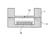
電極基板3には、凹部14を形成して、この凹部14の底面に振動板10に所定のギャップ16を置いて対向する電極15を形成し、この電極15と振動板10によって、振動板15を変位させて液室6の内容積を変化させるアクチュエータ部を構成している。この電極基板3の電極15上には振動板10との接触によって電極15が破損するのを防止するため、例えば0.1μm厚のSiO2などの絶縁層17を成膜している。なお、電極15を電極基板3の端部付近まで延設して外部駆動回路と接続手段を介して接続するための電極パッド部15aを形成している。
【0020】
この電極基板3は、ガラス基板、また表面に熱酸化膜3aを形成したSi基板上に、HF水溶液などでエッチングにより凹部14を形成し、この凹部14に窒化チタンなどの高耐熱性を有する電極材料をスパッタ、CVD、蒸着などの成膜技術で所望の厚さに成膜し、その後、フォトレジストを形成してエッチングすることにより、凹部14にのみ電極15を形成したものである。この電極基板3と振動板/液室基板1とは陽極接合、直接接合などのプロセスで接合している。
【0021】
ここでは、電極15は、シリコン基板にエッチングで形成した深さ0.3μmの凹部14内に窒化チタンを0.1μmの厚さにスパッタし形成している。したがって、このヘッドにおいては、電極基板3と振動板/液室基板1とを接合した後のギャップ16の長さ(振動板10と電極15との間隔)は、0.2μmとなっている。
【0022】
また、ノズル板4は、厚さ50μmのステンレス材(SUS)を用いて、ノズル5、液体抵抗部7及び共通インク液室へ外部からインクを供給するためのインク供給口19を形成している。
【0023】
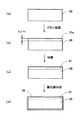
次に本発明に係るインクジェットヘッドの製造工程の第1実施形態について図5及び図6をも参照して説明する。
まず、図5(a)に示すような結晶面方位(110)の厚さ500μmのSi基板20を用いて、このSi基板20の表面に固体拡散法によりボロンを拡散することにより、同図(b)に示すように高濃度ボロン拡散層21aを形成する。
【0024】
より具体的には、Si基板20と固体拡散源(BNやB2O3)を対向させて750℃の温度の炉の中にセットする。この炉の中には0.25%の酸素を混入して窒素を流した状態にしておく。そして、その炉の温度を7℃/分のレートで1150℃の温度まで上昇させ、その状態で50分間保持した後、同じく7℃/分のレートで750℃の温度まで下げることにより、同図(b)に示すように、高濃度ボロン拡散層21が形成される。
【0025】
なお、この他BBr3を用いた気相拡散法、ボロンを高エネルギーで注入するイオン注入法又はB2O3を有機溶媒に分散させウエハ上にスピンコートする塗布拡散法でも、高濃度ボロン拡散層21aを形成できる。
【0026】
その後、Si基板20表面に形成されたB2O3層をフッ酸により除去することにより高濃度ボロンドープ層が形成される。
【0027】
この段階で得られた高濃度ボロンドープ層21a(Si基板20表面から厚さ方向に2μmの範囲)は、図7に短破線aで示すように表面(液室側と反対側の表面)が濃度の最も高くなる濃度分布を有している。
【0028】
そこで、次に、Si基板20表面を酸化することにより同図(c)に示すように酸化膜22を形成する。ここでは、酸化条件を、O2ガス6sccm、H2ガス9sccm、900℃−60分として約2000Åの厚さの酸化膜22を形成した。その後、同図(d)に示すようにSi基板20表面に形成した酸化膜22をフッ酸により除去することによりSi基板表面層が形成した。
【0029】
このときSi基板20表面から酸化膜22によってボロンが吸い出されるので、Si基板20の表面をなす高濃度ボロン拡散層21は、図7に実線bで示すように、振動板厚さ方向で内部に高濃度ボロンのピーク濃度を有する濃度分布となる。
【0030】
その後、ボロンの拡散により荒れている、Si基板20表面を直接接合できるようにするため、CMP(chemical-mechanical-polishing)によって表面粗さRa=0.5nm以下の表面性を有する高濃度ボロン拡散層21を得た。このCMPではSi基板20の最表層を1000Å以下の研磨量で面内均一に研磨できるので、高濃度ボロン拡散層21の変化は微量である。この場合、その研磨量を見込んで、ボロンを拡散させる拡散条件とSi基板20表面を酸化させる酸化条件を決定すればよい。
【0031】
次に、上述したようにして得られたシリコン基板20を図6(a)に示すように別途製作した電極基板3上に直接接合する。ここでは、減圧下でプリボンドされたものに温度900℃、1時間の熱処理を行って接合した。
【0032】
そして、同図(b)に示すように、厚さ500μmのSi基板40の上部表面を研磨して、厚さ100μmにした後、同図(c)に示すように、接合された電極基板3とSi基板20の全面にLP−CVDによりシリコン窒化膜24を成膜する。
【0033】
次いで、Si基板20上に形成されたシリコン窒化膜24上にレジストをコーティングし、露光、現象を行って液室6及び共通インク室8などに対応するレジストパターンを形成する。このとき、電極基板3の電極15と液室6のレジストパターンとが一致するようにIR光によりアライメントする。次に、Si基板20上のシリコン窒化膜24をドライエッチにより除去し、レジストを除去することにより、同図(d)に示すように、シリコン窒化膜24のパターン25を形成する。
【0034】
そして、KOH(10wt%)水溶液に浸し、Si基板20をエッチングすると、このときパターニングした側の開口部からエッチングが進みボロン濃度が1E20/cm3である深さに達した時、エッチングがストップ(エッチレートが極端に下がり)し、同図(e)に示すように液室6となる凹部と高濃度ボロンドープシリコン(高濃度ボロン拡散層21)からなる振動板10が形成される。これにノズル板4を接合することにより前述のようなインクジェットヘッドが得られる。
【0035】
このインクジェットヘッドにおける振動板10は、上述したように振動板10の厚さ方向でが図7に実線bで示すように振動板内部にピーク濃度を持ち、液室6側と液室6と反対側である電極15側に向かってそれぞれ低濃度になる高濃度ボロンの濃度勾配を有している。
【0036】
したがって、振動板10に作用する高濃度ボロンによる引っ張り応力は振動板10の内部が最も強くなるので、振動板10を液室6側に凸状に反らせようとする力が緩和され、振動板10を電極15側に変形変位させるために必要な駆動電圧が低くなって低電圧駆動が可能になり、しかも耐久性(繰り返し振動特性)も向上する。
【0037】
そこで、振動板10の電極15側表面の高濃度ボロンの濃度(単位はatom/cm3)と耐久性についての評価試験を行った。
実施例1:KOH水溶液を用いた異方性エッチングにより、前述した製造方法を用いて、図8に実線bで示すように電極側表面濃度が1.00E+20の振動板を製作した。なお、同図は、図9に示すように振動板10の電極15側表面を「0μm」として振動板厚さ方向に向かう濃度のプロフィルを示している(前述した図7も同様である。)。
【0038】
実施例2:実施例1と同様にして、図8に一点鎖線cで示すように電極側表面濃度が1E18の振動板を製作した。
実施例3:実施例1と同様にして、同図に二点鎖線dで示すように電極側表面濃度が1.00E+19の振動板を製作した。
【0039】
比較例1:KOH水溶液を用いた異方性エッチングにより、従来と同様にして同図に短破線aで示すように電極側表面にピーク濃度がある振動板を製作した。
【0040】
そして、これらの実施例1〜3及び比較例1の各振動板を有するインクジェットヘッドを駆動周波数10kHzで駆動して、特性劣化を生じる駆動回数を測定することで、耐久性(繰り返し振動特性)を評価した。この結果を図10に示している。
【0041】
同図から分かるように、比較例1では1.0*109回以下で特性劣化を生じたのに対し、実施例1のものでは1.0*109回以上5.0*109回まで、実施例2のものでは1.0*1010回以上、実施例3のものでは5.0*109回以上1.0*1010回までの駆動回数でも特性劣化を生じなかった。
【0042】
したがって、電極15側表面の高濃度ボロンの濃度が1*1020を越えない濃度にすることで、振動板10の応力をより緩和することができて、低電圧駆動化、耐久性の向上を図れる。より好ましくは、電極15側表面の高濃度ボロン濃度の8*1019を越えない濃度にすることで、一層耐久性の向上を図ることができる。
【0043】
次に、振動板10の液室6側表面の高濃度ボロンの濃度と電極15側表面の高濃度ボロンの濃度と関係についての評価試験を行った。
実施例4:EDP(エチレンジアミンピロカテコール)水溶液を用いた異方性エッチングにより、前述した製造方法を用いて、図11に実線bで示すように液室側表面濃度が電極側表面濃度に対して1E20以上高い振動板を製作した。
【0044】
実施例5:実施例4と同様にして、同図に長破線cで示すように液室側表面濃度が電極側表面濃度に対して略3E19高い振動板を製作した。
実施例6:実施例4と同様にして、同図に一点鎖線dで示すように液室側表面濃度と電極側表面濃度が略同じ振動板を製作した。
【0045】
実施例7:実施例4と同様にして、同図に二点鎖線eで示すように液室側表面濃度に対して電極側表面濃度が略3E19低い振動板を製作した。
実施例8:実施例4と同様にして、同図に長一点鎖線fで示すように液室側表面濃度に対して電極側表面濃度が略1E20低い振動板を製作した。
【0046】
比較例2:EDP(エチレンジアミンピロカテコール)水溶液を用いた異方性エッチングにより、従来と同様にして同図に短破線aで示すように電極側表面にピーク濃度がある振動板を製作した。
【0047】
そして、これらの実施例4〜8及び比較例2の各振動板を有するインクジェットヘッドを駆動周波数10kHzで駆動して、特性劣化を生じる駆動回数を測定することで、耐久性(繰り返し振動特性)を評価した。この結果を図12に示している。
【0048】
同図から分かるように、比較例2では1.0*109回以下で特性劣化を生じたのに対し、実施例4のものでは1.0*109回以上5.0*109回まで、実施例5〜7のものでは1.0*1010回以上、実施例8のものでは5.0*109以上1.0*1010回までの駆動回数でも特性劣化を生じなかった。
【0049】
したがって、振動板10の液室6側表面の高濃度ボロンの濃度と電極15側表面の高濃度ボロンの濃度との差が1*1020を越えないようにすることで耐久性が向上し、更に、その濃度の差を3*1019を越えないようにすることで更に耐久性が向上する。
【0050】
次に、本発明に係るインクジェットヘッドの製造方法の第2実施形態における高濃度ボロン拡散層の形成工程について図13をも参照して説明する。
この実施形態においては、同図(a)、(b)に示すように前述した図5(a)、(b)で説明したと同様な工程でシリコン基板20の表面に高濃度ボロン拡散層21aを形成した後、図13(c)に示すようにCMPによって高濃度ボロン拡散層21aの表面を研磨する。
【0051】
その後、Si基板20表面を酸化することにより同図(d)に示すようにシリコン基板20表面に高濃度ボロン拡散層21表面を含めて酸化膜25を形成する。その後は、図6で説明したと同様の工程を経てインクジェットヘッドを製作できる。
【0052】
すなわち、シリコン基板20に高濃度ボロンを拡散することによりB2O3層が形成され、そのB2O3層の下にボロンとシリコンの化合物層が形成される。そのため、図5(c)に示すようにこの化合物層を酸化して得られる酸化膜22の表面性は粗く、振動板/液室基板1との直接接合が困難であり、また、この酸化膜22はB2O3を含むために、絶縁耐圧が低く絶縁膜としては使用できないので、前述したように、酸化膜22を除去した後直接接合が可能なように研磨を行っている。
【0053】
これに対して、この実施形態では、先ず、CMPによる研磨を行ってボロンとシリコンの化合物層を除去するので、直接接合が可能な表面性を持つシリコン面(高濃度ボロン拡散層21表面)を得ることができる。そして、このシリコン表面を酸化して得られる酸化膜26の表面性は表面粗さRa=0.5nm以下であるので、酸化膜26を残したまま電極基板と直接接合することができるようになる。しかも、この酸化膜26はB2O3の含有量が少なく、絶縁耐圧が高く、かつ電極上に電荷が残留することを抑制するので、耐久性の向上とともに安定した駆動を行うことができる。
【0054】
なお、上記各実施形態においては本発明を静電型インクジェットヘッドに適用した例で説明したが、ピエゾ型インクジェットヘッドにも同様に適用することができ、またインク滴を吐出するインクジェットヘッド以外にも、例えば液体レジストを吐出するための液滴吐出ヘッドなどにも同様に適用することができる。また、本発明に係る液滴吐出ヘッドは、前述したようにプリンタ、ファクシミリ、複写装置等の画像記録装置或いは画像形成装置に備えることができ、これらの画像形成装置で液体を吐出するための液滴吐出装置として備えることもできる。
【0055】
【発明の効果】
以上説明したように、本発明に係る液滴吐出ヘッドによれば、振動板がP型不純物シリコン層からなり、P型不純物シリコン層のP型不純物濃度は、振動板の内部にピークを持ち、振動板の厚さ方向において、ピーク部から液室方向及び液室と逆方向に向かってそれぞれ低濃度になり、振動板の厚さ方向において、振動板の液室と反対側表面部で最小となる、分布を有する構成としたので、振動板の応力を緩和でき、低電圧駆動化及び耐久性(繰り返し振動特性)の向上を図ることができる。そして、本発明に係る画像形成装置、液滴吐出装置によれば、本発明に係る液滴吐出ヘッドを備えているので、低電圧駆動、耐久性の向上を図れる。
【0057】
また、振動板の液室と反対側の表面のP型不純物濃度が1*1020(atom/cm3)を越えないようにすることで、一層確実に振動板の応力を抑制でき、一層低電圧駆動化耐久性の向上を図れる。
【0059】
このヘッドを振動板と対向する電極を有し、振動板を静電力で変形変位させて液滴を吐出させる構成にすることで、信頼性の高い、優れた静電型液滴吐出ヘッドを得ることができる。
【0060】
本発明に係る液滴吐出ヘッドの製造方法によれば、シリコン基板にボロンを拡散した後、ボロン拡散層の表面を酸化するので、容易に本発明に係る液滴吐出ヘッドを得ることができる。この場合、また、シリコン基板にボロンを拡散した後、ボロン拡散層の表面を研磨処理し、次いでこのボロン拡散層の表面を酸化することで、信頼性の向上及び残留電荷の低減による安定駆動が可能な液滴吐出ヘッドを得ることができる。
【図面の簡単な説明】
【図1】本発明を適用した静電型インクジェットヘッドの分解斜視説明図
【図2】同ヘッドの透過状態で示す上面説明図
【図3】同ヘッドの液室長辺方向に沿う模式的断面説明図
【図4】同ヘッドの液室短辺方向に沿う模式的断面説明図
【図5】本発明を適用したインクジェットヘッドの製造方法の第1実施形態における高濃度ボロン拡散層の形成工程を説明する説明図
【図6】同第1実施形態におけるヘッドの製作工程を説明する説明図
【図7】図5(b)及び(e)の段階における高濃度ボロン拡散層の濃度分布図
【図8】振動板の電極側表面の高濃度ボロンの濃度と耐久性の評価試験の説明に供する濃度分布図
【図9】濃度分布図の説明に供する説明図
【図10】図8の各濃度分布を有する振動板の耐久性評価試験結果を説明する説明図
【図11】振動板の液室側表面の濃度と電極側表面の濃度との差と耐久性の評価試験の説明に供する濃度分布図
【図12】図11の各濃度分布を有する振動板の耐久性評価試験結果を説明する説明図
【図13】本発明を適用したインクジェットヘッドの製造方法の第2実施形態における高濃度ボロン拡散層の形成工程を説明する説明図
【符号の説明】
1…振動板/液室基板、3…電極基板、4…ノズル板、5…ノズル、6…液室、10…振動板、15…電極、20…Si基板、21…高濃度ボロン拡散層、22、26…酸化膜、23…シリコン窒化膜。[0001]
[Industrial application fields]
The present invention relates to a droplet discharge head, a manufacturing method thereof , an image forming apparatus, and a droplet discharge device.
[Prior art]
An ink jet head, which is a liquid droplet ejection head used in an image recording apparatus such as a printer, a facsimile machine, a copying apparatus, or an image forming apparatus, includes a nozzle that ejects ink droplets and a liquid chamber in which the nozzle communicates ( A pressure liquid chamber, a pressure chamber, a discharge chamber, an ink flow path, etc.) and a pressure generating means for generating pressure to pressurize the ink in the liquid chamber. An ink droplet is ejected from the nozzle by pressurizing the liquid chamber ink.
[0003]
As a conventional ink jet head, a piezoelectric type that discharges ink droplets by deforming and displacing a diaphragm that forms the wall surface of the liquid chamber using a piezoelectric element, or a heating resistor disposed in the liquid chamber is used. A bubble type that generates bubbles by ink film boiling and ejects ink droplets. A diaphragm that forms the wall of the liquid chamber (or an electrode integrated with it) and an electrode are used to deform the diaphragm with electrostatic force. There is an electrostatic type that discharges ink droplets by being displaced.
[0004]
In an inkjet head using a diaphragm such as the piezo type or the electrostatic type described above, the mechanical displacement characteristics of the diaphragm greatly affect the ink picking and discharging characteristics, and it is necessary to make the diaphragm thinner and more accurate. become.
[0005]
Therefore, in the conventional ink-jet head, as described in JP-A-6-23986, JP-A-6-71882, JP-A-9-267479, etc., boron is formed on the silicon substrate on which the diaphragm is formed. A diffused high-concentration boron diffusion layer is formed, and this silicon substrate is anisotropically etched to stop etching at the high-concentration boron diffusion layer, so that a diaphragm with the high-concentration boron diffusion layer is formed. .
[0006]
As described above, as a method for forming a high-concentration boron layer serving as a vibration plate on a silicon substrate, a solid diffusion method using a plate-like diffusion source (BN or B 2 O 3 ), or a vapor phase diffusion for diffusing Br 3 is used. There are known a method, an ion implantation method in which boron is implanted with high energy, or a coating diffusion method in which B 2 O 3 is dispersed in an organic solvent and spin-coated on a wafer.
[0007]
[Problems to be solved by the invention]
However, in the above-described solid diffusion method, vapor phase diffusion method, and coating diffusion method, boron is diffused from the surface of the silicon substrate (the surface that faces the electrode surface), so when the diaphragm is formed. In the thickness direction of the diaphragm, a high concentration region (peak concentration region) is likely to occur on the surface opposite to the liquid chamber. Even in the ion implantation method, the thickness of the diaphragm and the space on the apparatus are limited. Similarly, a peak concentration region is easily formed on the surface opposite to the liquid chamber.
[0008]
By the way, since the tensile stress becomes stronger as the boron concentration becomes higher in the boron doped layer, as described above, when the peak concentration region is located on the surface opposite to the liquid chamber, the vibration plate has a liquid chamber side. Therefore, a force to warp in a convex shape is applied.
[0009]
As described above, in the conventional ink jet head, since the tensile stress acting in the direction in which the diaphragm is warped toward the liquid chamber is applied, the drive voltage for displacing the diaphragm to the electrode side by a predetermined amount increases. Moreover, since the deformation is performed against the stress, there is a problem that the durability (repetitive vibration characteristics) of the diaphragm is lowered.
[0010]
The present invention has been made in view of the above problems, and has improved the durability of the diaphragm and improved the reliability of the droplet discharge head and the manufacturing method thereof, the image forming apparatus including the head, the droplet discharge An object is to provide an apparatus .
[0011]
[Means for Solving the Problems]
In order to solve the above problems, in the droplet discharge head according to the present invention, the vibration plate is made of a P-type impurity silicon layer, and the P-type impurity concentration of the P-type impurity silicon layer has a peak inside the vibration plate, In the thickness direction of the diaphragm, the concentration decreases from the peak portion toward the liquid chamber direction and the direction opposite to the liquid chamber, respectively, and in the thickness direction of the diaphragm, the minimum is the surface portion on the side opposite to the liquid chamber of the diaphragm. This is a configuration having a distribution . The image forming apparatus and the droplet discharge device according to the present invention include the droplet discharge head according to the present invention.
[0012]
Here, it is preferable that P-type impurity concentration in the liquid chamber and the opposite surface of the vibration plate does not exceed 1 * 10 20 (atom / cm 3).
[0013]
Furthermore , high-concentration boron can be used as the high-concentration P-type impurity. Further, it is preferable that the droplet discharge head has an electrode opposed to the diaphragm and discharges the droplet by deforming and displacing the diaphragm with an electrostatic force.
[0014]
A method for manufacturing a droplet discharge head according to the present invention is a method for manufacturing a droplet discharge head according to the present invention, wherein boron is diffused into a silicon substrate and then the surface of the boron diffusion layer is oxidized. is there. Here, after boron is diffused into the silicon substrate, it is preferable to polish the surface of the boron diffusion layer and then oxidize the surface of the boron diffusion layer.
[0015]
DETAILED DESCRIPTION OF THE INVENTION
Embodiments of the present invention will be described below with reference to the accompanying drawings. FIG. 1 is an exploded perspective view of an electrostatic ink jet head to which the present invention is applied, FIG. 2 is a top view of the head in a transparent state, and FIG. 3 is a schematic cross-sectional view of the head along the liquid chamber long side direction. FIG. 4 is a schematic cross-sectional explanatory diagram along the liquid chamber short side direction of the head.
[0016]
This inkjet head includes a vibration plate /
[0017]
On the vibration plate /
[0018]
Note that an insulating film such as 0.1 μm of SiO 2 is formed on the entire surface of the diaphragm /
[0019]
A
[0020]
The
[0021]
Here, the
[0022]
Further, the
[0023]
Next, a first embodiment of an ink jet head manufacturing process according to the present invention will be described with reference to FIGS.
First, by using a
[0024]
More specifically, the
[0025]
In addition, high-concentration boron diffusion can also be achieved by vapor phase diffusion using BBr 3 , ion implantation in which boron is implanted at high energy, or coating diffusion in which B 2 O 3 is dispersed in an organic solvent and spin-coated on the wafer.
[0026]
Thereafter, the B 2 O 3 layer formed on the surface of the
[0027]
The high-concentration boron-doped
[0028]
Therefore, next, the surface of the
[0029]
At this time, since boron is sucked out from the surface of the
[0030]
Thereafter, in order to directly bond the surface of the
[0031]
Next, the
[0032]
Then, as shown in FIG. 4B, the upper surface of the Si substrate 40 having a thickness of 500 μm is polished to a thickness of 100 μm, and then bonded to the
[0033]
Next, a resist is coated on the
[0034]
Then, when the
[0035]
As described above, the
[0036]
Accordingly, the tensile stress caused by the high-concentration boron acting on the
[0037]
Therefore, an evaluation test was performed on the concentration (unit: atom / cm 3 ) and durability of high-concentration boron on the
Example 1 A diaphragm having an electrode-side surface concentration of 1.00E + 20 as shown by a solid line b in FIG. 8 was manufactured by anisotropic etching using an aqueous KOH solution and using the manufacturing method described above. FIG. 9 shows a concentration profile in the direction of the diaphragm thickness with the
[0038]
Example 2 In the same manner as in Example 1, a diaphragm having an electrode-side surface concentration of 1E18 as shown by a one-dot chain line c in FIG.
Example 3 In the same manner as in Example 1, a diaphragm having an electrode-side surface concentration of 1.00E + 19 as shown by a two-dot chain line d in the same drawing was manufactured.
[0039]
Comparative Example 1: A diaphragm having a peak concentration on the surface on the electrode side as shown by a short broken line a in the same drawing was manufactured by anisotropic etching using a KOH aqueous solution as in the prior art.
[0040]
And the durability (repetitive vibration characteristics) is measured by driving the inkjet head having the diaphragms of Examples 1 to 3 and Comparative Example 1 at a driving frequency of 10 kHz, and measuring the number of driving times that causes characteristic deterioration. evaluated. The result is shown in FIG.
[0041]
As can be seen from the figure, in Comparative Example 1, the characteristic deterioration occurred in 1.0 * 10 9 times or less, whereas in Example 1, 1.0 * 10 9 times or more and 5.0 * 10 9 times. In the second example, the characteristics were not deteriorated even when the number of driving times was 1.0 * 10 10 times or more in the example 2, and 5.0 * 10 9 times or more and 1.0 * 10 10 times in the example 3.
[0042]
Therefore, by setting the concentration of the high-concentration boron on the surface on the
[0043]
Next, an evaluation test was performed on the relationship between the high concentration boron concentration on the
Example 4: By anisotropic etching using an EDP (ethylenediamine pyrocatechol) aqueous solution, using the manufacturing method described above, as shown by the solid line b in FIG. A diaphragm higher than 1E20 was manufactured.
[0044]
Example 5 In the same manner as in Example 4, a diaphragm having a liquid chamber side surface concentration approximately 3E19 higher than the electrode side surface concentration was manufactured as indicated by a long broken line c in FIG.
Example 6 In the same manner as in Example 4, as shown by the alternate long and short dash line d in the same drawing, a diaphragm having substantially the same liquid chamber side surface concentration and electrode side surface concentration was manufactured.
[0045]
Example 7 In the same manner as in Example 4, a diaphragm having an electrode-side surface concentration approximately 3E19 lower than the liquid chamber-side surface concentration was manufactured as indicated by a two-dot chain line e in FIG.
Example 8 In the same manner as in Example 4, a diaphragm having an electrode-side surface concentration approximately 1E20 lower than the liquid chamber-side surface concentration was manufactured as indicated by a long and short dashed line f in FIG.
[0046]
Comparative Example 2: A diaphragm having a peak concentration on the electrode-side surface as shown by a short broken line a in the same drawing was manufactured by anisotropic etching using an EDP (ethylenediamine pyrocatechol) aqueous solution in the same manner as before.
[0047]
Then, the durability (repetitive vibration characteristics) is measured by driving the inkjet head having the diaphragms of Examples 4 to 8 and Comparative Example 2 at a driving frequency of 10 kHz, and measuring the number of driving times that causes characteristic deterioration. evaluated. The result is shown in FIG.
[0048]
As can be seen from the figure, in Comparative Example 2, the characteristic deterioration occurred in 1.0 * 10 9 times or less, while in Example 4, 1.0 * 10 9 times or more and 5.0 * 10 9 times. Up to 1.0 * 10 10 times or more in Examples 5 to 7 and no deterioration in characteristics even in the case of Example 8 from 5.0 * 10 9 to 1.0 * 10 10 times. .
[0049]
Therefore, durability is improved by preventing the difference between the high concentration boron concentration on the
[0050]
Next, a process for forming a high-concentration boron diffusion layer in the second embodiment of the method for manufacturing an inkjet head according to the present invention will be described with reference to FIG.
In this embodiment, as shown in FIGS. 5A and 5B, the high-concentration
[0051]
Thereafter, the surface of the
[0052]
That is, a B 2 O 3 layer is formed by diffusing high-concentration boron in the
[0053]
In contrast, in this embodiment, since the compound layer of boron and silicon is first removed by polishing by CMP, a silicon surface (surface of the high-concentration boron diffusion layer 21) having a surface property capable of direct bonding is formed. Obtainable. Since the surface property of the
[0054]
In each of the above-described embodiments, the present invention has been described with reference to an example in which the present invention is applied to an electrostatic inkjet head. However, the present invention can be applied to a piezo inkjet head in the same manner, and other than an inkjet head that ejects ink droplets. For example, the present invention can be similarly applied to a droplet discharge head for discharging a liquid resist. Further, as described above, the liquid droplet ejection head according to the present invention can be provided in an image recording apparatus or an image forming apparatus such as a printer, a facsimile machine, a copying apparatus, etc., and a liquid for ejecting liquid by these image forming apparatuses. It can also be provided as a droplet discharge device.
[0055]
【The invention's effect】
As described above, according to the droplet discharge head according to the present invention, the diaphragm is made of the P-type impurity silicon layer, and the P-type impurity concentration of the P-type impurity silicon layer has a peak inside the diaphragm, In the thickness direction of the diaphragm, the concentration decreases from the peak portion toward the liquid chamber direction and the direction opposite to the liquid chamber, respectively, and in the thickness direction of the diaphragm, the minimum is the surface portion on the side opposite to the liquid chamber of the diaphragm. Since the configuration has a distribution, the stress of the diaphragm can be relieved, and low voltage driving and durability (repetitive vibration characteristics) can be improved. In addition, according to the image forming apparatus and the droplet discharge device according to the present invention, since the droplet discharge head according to the present invention is provided, low voltage drive and durability can be improved.
[0057]
In addition, by preventing the P-type impurity concentration on the surface of the diaphragm opposite to the liquid chamber from exceeding 1 * 10 20 (atoms / cm 3 ), the stress on the diaphragm can be suppressed more reliably, and the The voltage drive durability can be improved.
[0059]
This head has an electrode facing the diaphragm, and the diaphragm is deformed and displaced by electrostatic force to eject droplets, thereby obtaining a highly reliable and excellent electrostatic droplet discharge head. be able to.
[0060]
According to the method for manufacturing a droplet discharge head according to the present invention, since the surface of the boron diffusion layer is oxidized after diffusing boron into the silicon substrate, the droplet discharge head according to the present invention can be easily obtained. In this case, after boron is diffused into the silicon substrate, the surface of the boron diffusion layer is polished, and then the surface of the boron diffusion layer is oxidized, thereby improving the reliability and stable driving by reducing the residual charge. A possible droplet discharge head can be obtained.
[Brief description of the drawings]
FIG. 1 is an exploded perspective view of an electrostatic ink jet head to which the present invention is applied. FIG. 2 is a top view of the head in a transparent state. FIG. 3 is a schematic cross-sectional view along the liquid chamber long side direction. FIG. 4 is a schematic cross-sectional explanatory view along the direction of the short side of the liquid chamber of the head. FIG. 5 illustrates a process for forming a high-concentration boron diffusion layer in the first embodiment of a method for manufacturing an inkjet head to which the present invention is applied. FIG. 6 is an explanatory diagram for explaining the manufacturing process of the head according to the first embodiment. FIG. 7 is a concentration distribution diagram of the high-concentration boron diffusion layer at the stage of FIGS. 5B and 5E. ] Concentration distribution diagram for explaining the evaluation test of the concentration and durability of high-concentration boron on the electrode side surface of the diaphragm [FIG. 9] An explanatory diagram for explaining the concentration distribution diagram [FIG. 10] Each concentration distribution of FIG. Explanation of the results of the durability evaluation test of
DESCRIPTION OF
Claims (8)
前記振動板がP型不純物シリコン層からなり、
前記P型不純物シリコン層のP型不純物濃度は、前記振動板の内部にピークを持ち、前記振動板の厚さ方向において、ピーク部から液室方向及び液室と逆方向に向かってそれぞれ低濃度になり、前記振動板の厚さ方向において、前記振動板の液室と反対側表面部で最小となる、分布を有する
ことを特徴とする液滴吐出ヘッド。A liquid droplet that ejects liquid droplets from the nozzle by displacing and deforming the vibration plate, comprising a nozzle that ejects liquid droplets, a liquid chamber that communicates with the nozzle, and a diaphragm that forms a wall surface of the liquid chamber In the discharge head,
The diaphragm is made of a P-type impurity silicon layer,
The P-type impurity concentration of the P-type impurity silicon layer has a peak inside the diaphragm, and is low in the thickness direction of the diaphragm from the peak portion toward the liquid chamber and in the opposite direction to the liquid chamber. The droplet discharge head according to claim 1, wherein the droplet discharge head has a distribution that is minimized at a surface portion opposite to the liquid chamber of the diaphragm in the thickness direction of the diaphragm .
Priority Applications (1)
| Application Number | Priority Date | Filing Date | Title |
|---|---|---|---|
| JP2000219803A JP4001453B2 (en) | 2000-07-19 | 2000-07-19 | Droplet discharge head, method for manufacturing the same, image forming apparatus, and droplet discharge apparatus |
Applications Claiming Priority (1)
| Application Number | Priority Date | Filing Date | Title |
|---|---|---|---|
| JP2000219803A JP4001453B2 (en) | 2000-07-19 | 2000-07-19 | Droplet discharge head, method for manufacturing the same, image forming apparatus, and droplet discharge apparatus |
Publications (3)
| Publication Number | Publication Date |
|---|---|
| JP2002036541A JP2002036541A (en) | 2002-02-05 |
| JP2002036541A5 JP2002036541A5 (en) | 2006-03-02 |
| JP4001453B2 true JP4001453B2 (en) | 2007-10-31 |
Family
ID=18714518
Family Applications (1)
| Application Number | Title | Priority Date | Filing Date |
|---|---|---|---|
| JP2000219803A Expired - Fee Related JP4001453B2 (en) | 2000-07-19 | 2000-07-19 | Droplet discharge head, method for manufacturing the same, image forming apparatus, and droplet discharge apparatus |
Country Status (1)
| Country | Link |
|---|---|
| JP (1) | JP4001453B2 (en) |
Families Citing this family (1)
| Publication number | Priority date | Publication date | Assignee | Title |
|---|---|---|---|---|
| JP2005219426A (en) | 2004-02-09 | 2005-08-18 | Ricoh Co Ltd | Liquid discharge head, liquid cartridge, liquid discharge device, image forming device and liquid discharge head manufacturing method |
-
2000
- 2000-07-19 JP JP2000219803A patent/JP4001453B2/en not_active Expired - Fee Related
Also Published As
| Publication number | Publication date |
|---|---|
| JP2002036541A (en) | 2002-02-05 |
Similar Documents
| Publication | Publication Date | Title |
|---|---|---|
| US7121650B2 (en) | Piezoelectric ink-jet printhead | |
| JP2006069152A (en) | Inkjet head and its manufacturing process | |
| JP4001453B2 (en) | Droplet discharge head, method for manufacturing the same, image forming apparatus, and droplet discharge apparatus | |
| JP2001260355A (en) | Ink jet head and method of manufacture | |
| JP2003011365A (en) | Ink jet head and its manufacturing method | |
| JP6608181B2 (en) | Method for manufacturing liquid discharge head | |
| JP4070175B2 (en) | Droplet ejection head, inkjet recording apparatus, image forming apparatus, and apparatus for ejecting droplets | |
| JP2001260367A (en) | Method for manufacturing liquid drop discharge head | |
| JP5807362B2 (en) | Method for manufacturing liquid jet head | |
| JP3963341B2 (en) | Droplet discharge head | |
| JP2003011359A (en) | Ink jet head and its manufacturing method | |
| JP2001171111A (en) | Method for manufacturing ink jet head | |
| JP2007038452A (en) | Electrostatic actuator, its manufacturing method, liquid droplet delivering head, its manufacturing method, device and liquid droplet delivering apparatus | |
| JP2002248763A (en) | Ink-jet head and production method therefor | |
| JP4306364B2 (en) | Droplet discharge head manufacturing method, droplet discharge head, and printer including the discharge head | |
| JP2002144589A (en) | Ink jet head | |
| JP4120317B2 (en) | Inkjet head manufacturing method | |
| JP2002086738A (en) | Method of making liquid jet head | |
| JP2002160361A (en) | Ink drop ejecting head | |
| JP4307745B2 (en) | Droplet discharge head and inkjet recording apparatus | |
| JP2001347658A (en) | Electrostatic actuator, its manufacturing method and liquid drop discharge head | |
| JP2005028644A (en) | Inkjet head, manufacturing method therefor, and inkjet recording apparatus | |
| JP4100447B2 (en) | Silicon substrate having recess and inkjet head | |
| JP3642271B2 (en) | Inkjet head manufacturing method | |
| KR100400228B1 (en) | Inkjet printhead and manufacturing method thereof |
Legal Events
| Date | Code | Title | Description |
|---|---|---|---|
| A621 | Written request for application examination |
Free format text: JAPANESE INTERMEDIATE CODE: A621 Effective date: 20041125 |
|
| A521 | Written amendment |
Free format text: JAPANESE INTERMEDIATE CODE: A523 Effective date: 20060108 |
|
| A977 | Report on retrieval |
Free format text: JAPANESE INTERMEDIATE CODE: A971007 Effective date: 20070215 |
|
| A131 | Notification of reasons for refusal |
Free format text: JAPANESE INTERMEDIATE CODE: A131 Effective date: 20070223 |
|
| A521 | Written amendment |
Free format text: JAPANESE INTERMEDIATE CODE: A523 Effective date: 20070421 |
|
| A131 | Notification of reasons for refusal |
Free format text: JAPANESE INTERMEDIATE CODE: A131 Effective date: 20070608 |
|
| A521 | Written amendment |
Free format text: JAPANESE INTERMEDIATE CODE: A523 Effective date: 20070723 |
|
| TRDD | Decision of grant or rejection written | ||
| A01 | Written decision to grant a patent or to grant a registration (utility model) |
Free format text: JAPANESE INTERMEDIATE CODE: A01 Effective date: 20070814 |
|
| A61 | First payment of annual fees (during grant procedure) |
Free format text: JAPANESE INTERMEDIATE CODE: A61 Effective date: 20070814 |
|
| FPAY | Renewal fee payment (prs date is renewal date of database) |
Free format text: PAYMENT UNTIL: 20100824 Year of fee payment: 3 |
|
| R150 | Certificate of patent (=grant) or registration of utility model |
Free format text: JAPANESE INTERMEDIATE CODE: R150 |
|
| FPAY | Renewal fee payment (prs date is renewal date of database) |
Free format text: PAYMENT UNTIL: 20100824 Year of fee payment: 3 |
|
| FPAY | Renewal fee payment (prs date is renewal date of database) |
Free format text: PAYMENT UNTIL: 20110824 Year of fee payment: 4 |
|
| FPAY | Renewal fee payment (prs date is renewal date of database) |
Free format text: PAYMENT UNTIL: 20110824 Year of fee payment: 4 |
|
| FPAY | Renewal fee payment (prs date is renewal date of database) |
Free format text: PAYMENT UNTIL: 20120824 Year of fee payment: 5 |
|
| FPAY | Renewal fee payment (prs date is renewal date of database) |
Free format text: PAYMENT UNTIL: 20120824 Year of fee payment: 5 |
|
| FPAY | Renewal fee payment (prs date is renewal date of database) |
Free format text: PAYMENT UNTIL: 20130824 Year of fee payment: 6 |
|
| LAPS | Cancellation because of no payment of annual fees |