JP4000000B2 - Magnetic random access memory and manufacturing method thereof - Google Patents
Magnetic random access memory and manufacturing method thereof Download PDFInfo
- Publication number
- JP4000000B2 JP4000000B2 JP2002118215A JP2002118215A JP4000000B2 JP 4000000 B2 JP4000000 B2 JP 4000000B2 JP 2002118215 A JP2002118215 A JP 2002118215A JP 2002118215 A JP2002118215 A JP 2002118215A JP 4000000 B2 JP4000000 B2 JP 4000000B2
- Authority
- JP
- Japan
- Prior art keywords
- write
- random access
- magnetic random
- access memory
- line
- Prior art date
- Legal status (The legal status is an assumption and is not a legal conclusion. Google has not performed a legal analysis and makes no representation as to the accuracy of the status listed.)
- Expired - Fee Related
Links
Images


Landscapes
- Semiconductor Memories (AREA)
- Hall/Mr Elements (AREA)
- Mram Or Spin Memory Techniques (AREA)
Description
【0001】
【発明の属する技術分野】
本発明は、トンネル型磁気抵抗(Tunneling Magneto Resistive)効果により“1”,“0”−情報を記憶するTMR素子を利用してメモリセルを構成した磁気ランダムアクセスメモリ(MRAM: Magnetic Random Access Memory)に関する。
【0002】
【従来の技術】
近年、新たな原理により情報を記憶するメモリが数多く提案されているが、そのうちの一つに、Roy Scheuerlein et.al.によって提案されたトンネル型磁気抵抗(Tunneling Magneto Resistive: 以後、TMRと表記する。) 効果を利用したメモリがある(例えば、ISSCC2000 Technical Digest p.128「A 10ns Read and Write Non-Volatile Memory Array Using a Magnetic Tunnel Junction and FET Switch in each Cell」を参照)。
【0003】
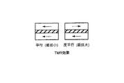
磁気ランダムアクセスメモリは、TMR素子により“1”,“0”−情報を記憶する。TMR素子は、図96に示すように、2つの磁性層(強磁性層)により絶縁層(トンネルバリア)を挟んだ構造を有する。TMR素子に記憶される情報は、2つの磁性層のスピンの向きが平行か又は反平行かによって判断される。
【0004】
ここで、図97に示すように、平行とは、2つの磁性層のスピンの向き(磁化の方向)が同じであることを意味し、反平行とは、2つの磁性層のスピンの向きが逆向きであることを意味する(矢印の向きがスピンの向きを示している。)。
【0005】
なお、通常、2つの磁性層の一方側には、反強磁性層が配置される。反強磁性層は、一方側の磁性層のスピンの向きを固定し、他方側のスピンの向きのみを変えることにより情報を容易に書き換えるための部材である。
【0006】
スピンの向きが固定された磁性層は、固定層又はピン層と呼ばれる。また、書き込みデータに応じて、スピンの向きを自由に変えることができる磁性層は、自由層又は記憶層と呼ばれる。
【0007】
図97に示すように、2つの磁性層のスピンの向きが平行となった場合、これら2つの磁性層に挟まれた絶縁層(トンネルバリア)のトンネル抵抗は、最も低くなる。この状態が“1”−状態である。また、2つの磁性層のスピンの向きが反平行となった場合、これら2つの磁性層に挟まれた絶縁層(トンネルバリア)のトンネル抵抗は、最も高くなる。この状態が“0”−状態である。
【0008】
次に、図98を参照しつつ、TMR素子に対する書き込み動作原理について簡単に説明する。
【0009】
TMR素子は、互いに交差する書き込みワード線とデータ選択線(読み出し/書き込みビット線)との交点に配置される。そして、書き込みは、書き込みワード線及びデータ選択線に電流を流し、両配線に流れる電流により作られる磁界を用いて、TMR素子のスピンの向きを平行又は反平行にすることにより達成される。
【0010】
例えば、TMR素子の磁化容易軸がX方向であり、X方向に書き込みワード線が延び、X方向に直交するY方向にデータ選択線が延びている場合、書き込み時には、書き込みワード線に、一方向に向かう電流を流し、データ選択線に、書き込みデータに応じて、一方向又は他方向に向かう電流を流す。
【0011】
データ選択線に一方向に向かう電流を流すとき、TMR素子のスピンの向きは、平行(“1”−状態)となる。一方、データ選択線に他方向に向かう電流を流すとき、TMR素子のスピンの向きは、反平行(“0”−状態)となる。
【0012】
TMR素子のスピンの向きが変わるしくみは、次の通りである。
【0013】
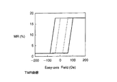
図99のTMR曲線に示すように、TMR素子の長辺(Easy-Axis)方向に磁界Hxをかけると、TMR素子の抵抗値は、例えば、17%程度変化する。この変化率、即ち、変化の前後の抵抗値の比は、MR比と呼ばれる。
【0014】
なお、MR比は、磁性層の性質により変化する。現在では、MR比が50%程度のTMR素子も得られている。
【0015】
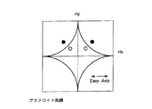
TMR素子には、Easy-Axis方向の磁界HxとHard-Axis方向の磁界Hyとの合成磁界がかかる。図100の実線に示すように、Hard-Axis方向の磁界Hyの大きさによって、TMR素子の抵抗値を変えるために必要なEasy-Axis方向の磁界Hxの大きさも変化する。この現象を利用することにより、アレイ状に配置されるメモリセルのうち、選択された書き込みワード線及び選択されたデータ選択線の交点に存在するTMR素子のみにデータを書き込むことができる。
【0016】
この様子をさらに図100のアステロイド曲線を用いて説明する。
TMR素子のアステロイド曲線は、例えば、図100の実線で示すようになる。即ち、Easy-Axis方向の磁界HxとHard-Axis方向の磁界Hyとの合成磁界の大きさがアステロイド曲線(実線)の外側(例えば、黒丸の位置)にあれば、磁性層のスピンの向きを反転させることができる。
【0017】
逆に、Easy-Axis方向の磁界HxとHard-Axis方向の磁界Hyとの合成磁界の大きさがアステロイド曲線(実線)の内側(例えば、白丸の位置)にある場合には、磁性層のスピンの向きを反転させることはできない。
【0018】
従って、Easy-Axis方向の磁界Hxの大きさとHard-Axis方向の磁界Hyの大きさを変え、合成磁界の大きさのHx−Hy平面内における位置を変えることにより、TMR素子に対するデータの書き込みを制御できる。
【0019】
なお、読み出しは、選択されたTMR素子に電流を流し、そのTMR素子の抵抗値を検出することにより容易に行うことができる。
【0020】
例えば、TMR素子に直列にスイッチ素子を接続し、選択された読み出しワード線に接続されるスイッチ素子のみをオン状態として電流経路を作る。その結果、選択されたTMR素子のみに電流が流れるため、そのTMR素子のデータを読み出すことができる。
【0021】
【発明が解決しようとする課題】
磁気ランダムアクセスメモリにおいては、上述ように、データ書き込みは、書き込みワード線とデータ選択線(読み出し/書き込みビット線)に,それぞれ、書き込み電流を流し、これにより発生する合成磁界をTMR素子に作用させることにより行う。
【0022】
従って、データ書き込みを効率よく行うためには、この合成磁界を、効率よく、TMR素子に与えることが重要となる。合成磁界が効率よくTMR素子に印加されれば、書き込み動作の信頼性が向上し、さらに、書き込み電流を減らし、低消費電力化を実現することができる。
【0023】
しかし、書き込みワード線及びデータ選択線にそれぞれ流れる書き込み電流により発生する合成磁界を、効率よく、TMR素子に作用させるために有効なデバイス構造については、十分に検討されていない。即ち、このようなデバイス構造は、実際に、合成磁界が効率よくTMR素子に加わることはもちろん、簡単に製造できるか否かという製造プロセスの面からも検討される必要がある。
【0024】
本発明は、このような問題を解決するためになされたもので、その目的は、磁気ランダムアクセスメモリにおいて、書き込み動作時、合成磁界を、効率よく、TMR素子に作用させることができるデバイス構造及びその製造方法を提案することにある。
【0025】
【課題を解決するための手段】
(1) ▲1▼ 本発明の磁気ランダムアクセスメモリは、半導体基板の上部に形成され、磁気抵抗効果を利用してデータを記憶するメモリセルと、前記メモリセルの直下に配置され、第1方向に延びる第1書き込み線と、前記メモリセルの直上に配置され、前記第1方向に交差する第2方向に延びる第2書き込み線と、前記第1書き込み線の側面を覆い、前記第1書き込み線の上面よりも下部に窪んでいる第1ヨーク材とを備える。
【0026】
前記第1ヨーク材は、前記第1書き込み線の側面のみを覆っている。前記第1ヨーク材は、前記第1書き込み線の下面を覆っている。
【0027】
本発明の磁気ランダムアクセスメモリは、前記第2書き込み線の表面の一部を覆う第2ヨーク材をさらに備える。前記第2ヨーク材は、前記第2書き込み線の上面及び側面を覆っている。前記第2ヨーク材は、前記第2書き込み線の上面のみを覆っている。前記第2ヨーク材は、前記第2書き込み線の側面のみを覆っている。
【0028】
前記第1及び第2書き込み線のうちの1つは、前記メモリセルに電気的に接続され、読み出しビット線としても機能する。
【0029】
▲2▼ 本発明の磁気ランダムアクセスメモリは、半導体基板の上部に形成され、磁気抵抗効果を利用してデータを記憶するメモリセルと、前記メモリセルの直下に配置され、第1方向に延びる第1書き込み線と、前記メモリセルの直上に配置され、前記第1方向に交差する第2方向に延びる第2書き込み線と、前記第2書き込み線の側面を覆い、前記第2書き込み線の下面よりも上部に窪んでいる第1ヨーク材とを備える。
【0030】
前記第1ヨーク材は、前記第2書き込み線の側面のみを覆っている。前記第1ヨーク材は、前記第2書き込み線の上面を覆っている。
【0031】
本発明の磁気ランダムアクセスメモリは、前記第1書き込み線の表面の一部を覆う第2ヨーク材をさらに備える。前記第2ヨーク材は、前記第1書き込み線の下面及び側面を覆っている。前記第2ヨーク材は、前記第1書き込み線の下面のみを覆っている。前記第2ヨーク材は、前記第1書き込み線の側面のみを覆っている。
【0032】
前記第1及び第2書き込み線のうちの1つは、前記メモリセルに電気的に接続され、読み出しビット線としても機能する。
【0033】
▲3▼ 本発明の磁気ランダムアクセスメモリは、半導体基板の上部に積み重ねられ、磁気抵抗効果を利用してデータを記憶する第1及び第2メモリセルと、前記第1及び第2メモリセルの間に配置され、第1方向に延びる第1書き込み線と、前記第1書き込み線の側面のみを覆い、前記第1書き込み線の上面よりも下部に窪み、前記第1書き込み線の下面よりも上部に窪んでいる第1ヨーク材とを備える。
【0034】
前記第2メモリセルは、前記第1メモリセルよりも上に配置される。本発明の磁気ランダムアクセスメモリは、前記第1メモリセルの直下に配置され、前記第1方向に交差する第2方向に延びる第2書き込み線と、前記第2メモリセルの直上に配置され、前記第2方向に延びる第3書き込み線とをさらに備える。
【0035】
本発明の磁気ランダムアクセスメモリは、前記第2書き込み線の側面のみを覆い、前記第2書き込み線の上面よりも下部に窪んでいる第2ヨーク材と、前記第3書き込み線の側面のみを覆い、前記第3書き込み線の下面よりも上部に窪んでいる第3ヨーク材とをさらに備える。
【0036】
前記第1書き込み線は、前記第1及び第2メモリセルから離れている。前記第1書き込み線は、前記第1及び第2メモリセルに接触している。
【0037】
▲4▼ 本発明の磁気ランダムアクセスメモリは、半導体基板の上部において前記半導体基板の表面に平行な方向に並んで配置され、磁気抵抗効果を利用してデータを記憶する複数のメモリセルと、前記複数のメモリセルに共有され、第1方向に延びる第1書き込み線と、前記複数のメモリセルに個別に設けられ、前記第1方向に交差する第2方向に延びる複数の第2書き込み線と、前記第1書き込み線の側面のみを覆い、前記第1書き込み線の前記複数のメモリセル側の面よりも前記複数のメモリセル側に対し反対側に窪んでいる第1ヨーク材と、前記複数の第2書き込み線の側面のみを覆い、前記第2書き込み線の前記複数のメモリセル側の面よりも前記複数のメモリセル側に対し反対側に窪んでいる第2ヨーク材とを備える。
【0038】
前記第1書き込み線は、前記複数のメモリセルの直上に配置され、前記複数のメモリセルの一端に接触している。前記複数のメモリセルの他端は、共通接続されている。前記複数の第2書き込み線は、前記複数のメモリセルの直下に配置され、前記複数のメモリセルから離れている。
【0039】
前記第1書き込み線は、前記複数のメモリセルの直上に配置され、前記複数のメモリセルから離れている。前記複数の第2書き込み線は、前記複数のメモリセルの直下に配置され、前記複数のメモリセルの一端に接触している。前記複数のメモリセルの他端は、共通接続されている。
【0040】
(2) ▲1▼ 本発明の磁気ランダムアクセスメモリの製造方法は、半導体基板の上部に絶縁層を形成する工程と、前記絶縁層に配線溝を形成する工程と、前記配線溝の底部及び側壁部にヨーク材を形成する工程と、前記配線溝内に導電材を満たして書き込み線を形成する工程と、前記ヨーク材の一部をエッチングして前記ヨーク材を前記書き込み線の上面よりも下部に窪ませる工程と、前記書き込み線の直上にTMR素子を形成する工程とを備える。
【0041】
前記ヨーク材は、CVD法により、前記絶縁層上並びに前記配線溝の底部上及び側壁部上に形成された後、CMP法により、前記配線溝の底部及び側壁部に残存させられる。
【0042】
前記導電材は、CVD法により、前記絶縁層上及び前記配線溝内に形成された後、CMP法により、前記配線溝内のみに残存させられる。
【0043】
▲2▼ 本発明の磁気ランダムアクセスメモリの製造方法は、半導体基板の上部に絶縁層を形成する工程と、前記絶縁層に配線溝を形成する工程と、前記配線溝の側壁部のみにヨーク材を形成する工程と、前記配線溝内に導電材を満たして書き込み線を形成する工程と、前記ヨーク材の一部をエッチングして前記ヨーク材を前記書き込み線の上面よりも下部に窪ませる工程と、前記書き込み線の直上にTMR素子を形成する工程とを備える。
【0044】
前記ヨーク材は、CVD法により、前記絶縁層上並びに前記配線溝の底部上及び側壁部上に形成された後、RIE法により、前記配線溝の側壁部のみに残存させられる。
【0045】
前記導電材は、CVD法により、前記絶縁層上及び前記配線溝内に形成された後、CMP法により、前記配線溝内のみに残存させられる。
【0046】
▲3▼ 本発明の磁気ランダムアクセスメモリの製造方法は、半導体基板の上部にTMR素子を形成する工程と、前記TMR素子上に第1絶縁層を形成する工程と、前記TMR素子上の前記第1絶縁層に配線溝を形成する工程と、前記配線溝の側壁部のみに第2絶縁層を形成する工程と、前記配線溝内に導電材を満たして書き込み線を形成する工程と、前記第2絶縁層の一部をエッチングして前記第2絶縁層を前記書き込み線の下面近傍のみに残存させる工程と、前記第2絶縁層が取り除かれた前記配線溝の側壁部にヨーク材を形成する工程とを備える。
【0047】
前記ヨーク材は、前記配線溝の側壁部に形成されると同時に、前記書き込み線の上面にも形成される。
【0048】
前記ヨーク材は、CVD法により、前記配線溝の側壁部、前記第1絶縁層上及び前記書き込み線上に形成された後、CMP法により、前記配線溝の側壁部に残存させられる。
【0049】
前記ヨーク材は、CVD法により、前記配線溝の側壁部、前記第1絶縁層上及び前記書き込み線上に形成された後、RIE法により、前記配線溝の側壁部に残存させられる。
【0050】
前記ヨーク材は、CVD法により、前記配線溝の側壁部、前記第1絶縁層上及び前記書き込み線上に形成された後、RIE法により、前記配線溝の側壁部及び前記書き込み線上に残存させられる。
【0051】
前記第2絶縁層のエッチング量は、前記ヨーク材の下面が前記書き込み線の上面と下面との間に配置されることを条件に決定される。
【0052】
前記導電材は、CVD法により、前記絶縁層上及び前記配線溝内に形成された後、CMP法により、前記配線溝内のみに残存させられる。
【0053】
▲4▼ 本発明の磁気ランダムアクセスメモリの製造方法は、半導体基板の上部にTMR素子を形成する工程と、前記TMR素子上に絶縁層を形成する工程と、前記TMR素子上の前記絶縁層に配線溝を形成する工程と、前記配線溝内に導電材を満たして書き込み線を形成する工程と、前記絶縁層の一部をエッチングして前記絶縁層を前記書き込み線の下面近傍のみに残存させる工程と、前記絶縁層が取り除かれることにより露出した前記書き込み線の側面にヨーク材を形成する工程とを備える。
【0054】
前記ヨーク材は、CVD法により、前記絶縁層上並びに前記書き込み線の上面及び側面に形成された後、RIE法により、前記書き込み線の側面のみに残存させられる。
【0055】
前記絶縁層のエッチング量は、前記ヨーク材の下面が前記書き込み線の上面と下面との間に配置されることを条件に決定される。
【0056】
前記導電材は、CVD法により、前記絶縁層上及び前記配線溝内に形成された後、CMP法により、前記配線溝内のみに残存させられる。
【0057】
【発明の実施の形態】
以下、図面を参照しながら、本発明の磁気ランダムアクセスメモリの例について詳細に説明する。
【0058】
1. 参考例1
まず、本発明の磁気ランダムアクセスメモリの例を説明するに当たり、その前提となるデバイス構造について説明する。
【0059】
なお、このデバイス構造は、本発明の磁気ランダムアクセスメモリの例を簡単に説明することを目的に示すもので、本発明が、このデバイス構造に限定されるというものではない。
【0060】
図1及び図2は、それぞれ、本発明の磁気ランダムアクセスメモリの例の前提となるデバイス構造を示している。
【0061】
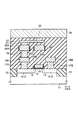
半導体基板(例えば、p型シリコン基板、p型ウェル領域など)11内には、STI( Shallow Trench Isolation )構造を有する素子分離絶縁層12が形成される。素子分離絶縁層12により取り囲まれた領域は、読み出し選択スイッチ(例えば、MOSトランジスタ、ダイオードなど)が形成される素子領域となる。
【0062】
図1のデバイス構造では、読み出し選択スイッチは、MOSトランジスタ(nチャネル型MOSトランジスタ)から構成される。半導体基板11上には、ゲート絶縁層13、ゲート電極14及び側壁絶縁層15が形成される。ゲート電極14は、X方向に延びており、読み出し動作時に、読み出しセル(TMR素子)を選択するための読み出しワード線として機能する。
【0063】
半導体基板11内には、ソース領域(例えば、n型拡散層)16−S及びドレイン領域(例えば、n型拡散層)16−Dが形成される。ゲート電極(読み出しワード線)14は、ソース領域16−Sとドレイン領域16−Dの間のチャネル領域上に配置される。
【0064】
図2のデバイス構造では、読み出し選択スイッチは、ダイオードから構成される。半導体基板11内には、カソード領域(例えば、n型拡散層)16a及びアノード領域(例えば、p型拡散層)16bが形成される。
【0065】
第1金属配線層を構成する金属層のうちの1つは、複数のコンタクトプラグを縦に積み重ねるための中間層18Aとして機能し、他の1つは、ソース線18B(図1の場合)又は読み出しワード線18B(図2の場合)として機能する。
【0066】
図1のデバイス構造の場合、中間層18Aは、コンタクトプラグ17Aにより、読み出し選択スイッチ(MOSトランジスタ)のドレイン領域16−Dに電気的に接続される。ソース線18Bは、コンタクトプラグ17Bにより、読み出し選択スイッチのソース領域16−Sに電気的に接続される。ソース線18Bは、ゲート電極(読み出しワード線)14と同様に、X方向に延びている。
【0067】
図2のデバイス構造の場合、中間層18Aは、コンタクトプラグ17Aにより、読み出し選択スイッチ(ダイオード)のアノード領域16bに電気的に接続される。読み出しワード線18Bは、コンタクトプラグ17Bにより、読み出し選択スイッチのカソード領域16aに電気的に接続される。読み出しワード線18Bは、X方向に延びている。
【0068】
第2金属配線層を構成する金属層のうちの1つは、複数のコンタクトプラグを縦に積み重ねるための中間層20Aとして機能し、他の1つは、書き込みワード線20Bとして機能する。中間層20Aは、コンタクトプラグ19により、中間層18Aに電気的に接続される。書き込みワード線20Bは、例えば、X方向に延びている。
【0069】
第3金属配線層を構成する金属層のうちの1つは、TMR素子23の下部電極22として機能する。下部電極22は、コンタクトプラグ21により、中間層20Aに電気的に接続される。TMR素子23は、下部電極22上に搭載される。ここで、TMR素子23は、書き込みワード線20Bの直上に配置されると共に、X方向に長い長方形状(磁化容易軸がX方向)に形成される。
【0070】
第4金属配線層を構成する金属層のうちの1つは、データ選択線(読み出し/書き込みビット線)24として機能する。データ選択線24は、TMR素子23に電気的に接続されると共に、Y方向に延びている。
【0071】
なお、TMR素子23の構造に関しては、特に、限定されない。図96に示すような構造であってもよいし、その他の構造であってもよい。また、TMR素子23は、複数ビットのデータを記憶できる多値記憶型であっても構わない。
【0072】
TMR素子23の強磁性層としては、特に制限はないが、例えば、Fe,Co,Ni又はこれらの合金、スピン分極率の大きいマグネタイト、CrO2,RXMnO3−y(R: 希土類、X: Ca,Ba,Sr)などの酸化物の他、NiMnSb,PtMnSbなどのホイスラー合金などを用いることができる。
【0073】
強磁性層には、Ag,Cu,Au,Al,Mg,Si,Bi,Ta,B,C,O,N,Pd,Pt,Zr,Ir,W,Mo,Nbなどの非磁性元素が多少含まれていても、強磁性を失わないかぎり、全く問題ない。
【0074】
強磁性層の厚さは、あまりに薄いと、超常磁性となってしまう。そこで、強磁性層の厚さは、少なくとも超常磁性とならない程度の厚さが必要である。具体的には、強磁性層の厚さは、0.1nm以上、好ましくは、0.4nm以上100nm以下に設定される。
【0075】
TMR素子23の反磁性層としては、例えば、Fe−Mn,Pt−Mn,Pt−Cr−Mn,Ni−Mn,Ir−Mn,NiO,Fe2O3などを用いることができる。
【0076】
TMR素子23の絶縁層(トンネルバリア)としては、例えば、Al2O3,SiO2,MgO,AlN,Bi2O3,MgF2,CaF2,SrTiO2,AlLaO3などの誘電体を使用することができる。これらは、酸素欠損、窒素欠損、フッ素欠損などが存在していてもかまわない。
【0077】
絶縁層(トンネルバリア)の厚さは、できるだけ薄い方がよいが、特に、その機能を実現するための決まった制限はない。但し、製造上、絶縁層の厚さは、10nm以下に設定される。
【0078】
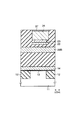
2. 参考例2
次に、参考例1のデバイス構造に対して、TMR素子に磁界を効率よく集中させるために提案されたデバイス構造について説明する。
【0079】
図3乃至図6は、本発明の磁気ランダムアクセスメモリの例の前提となるデバイス構造を示している。なお、図3及び図5は、Y方向の断面であり、図4は、図3のTMR素子部のX方向の断面であり、図6は、図5のTMR素子部のX方向の断面である。X方向とY方向は、互いに直交する。
【0080】
半導体基板(例えば、p型シリコン基板、p型ウェル領域など)11内には、STI( Shallow Trench Isolation )構造を有する素子分離絶縁層12が形成される。素子分離絶縁層12により取り囲まれた領域は、読み出し選択スイッチ(例えば、MOSトランジスタ)が形成される素子領域となる。
【0081】
本例のデバイス構造では、読み出し選択スイッチは、MOSトランジスタ(nチャネル型MOSトランジスタ)から構成される。半導体基板11上には、ゲート絶縁層13、ゲート電極14及び側壁絶縁層15が形成される。ゲート電極14は、X方向に延びており、読み出し動作時に、読み出しセル(TMR素子)を選択するための読み出しワード線として機能する。
【0082】
半導体基板11内には、ソース領域(例えば、n型拡散層)16−S及びドレイン領域(例えば、n型拡散層)16−Dが形成される。ゲート電極(読み出しワード線)14は、ソース領域16−Sとドレイン領域16−Dの間のチャネル領域上に配置される。
【0083】
第1金属配線層を構成する金属層のうちの1つは、複数のコンタクトプラグを縦に積み重ねるための中間層18Aとして機能し、他の1つは、ソース線18Bとして機能する。
【0084】
中間層18Aは、コンタクトプラグ17Aにより、読み出し選択スイッチ(MOSトランジスタ)のドレイン領域16−Dに電気的に接続される。ソース線18Bは、コンタクトプラグ17Bにより、読み出し選択スイッチのソース領域16−Sに電気的に接続される。ソース線18Bは、例えば、ゲート電極(読み出しワード線)14と同様に、X方向に延びている。
【0085】
第2金属配線層を構成する金属層のうちの1つは、複数のコンタクトプラグを縦に積み重ねるための中間層20Aとして機能し、他の1つは、書き込みワード線20Bとして機能する。中間層20Aは、コンタクトプラグ19により、中間層18Aに電気的に接続される。書き込みワード線20Bは、例えば、ゲート電極(読み出しワード線)14と同様に、X方向に延びている。
【0086】
本例のデバイス構造では、中間層20A及び書き込みワード線20Bの下面及び側面は、高い透磁率を有する材料、即ち、ヨーク材( yoke material )25A,25Bにより覆われている。ここで使用されるヨーク材25A,25Bは、導電性を有するものに限定される。
【0087】
磁束は、高い透磁率を有する材料に集中する性質があるため、この高い透磁率を有する材料を磁力線の牽引役として使用すれば、書き込み動作時、書き込みワード線20Bに流れる書き込み電流により発生する磁界Hyを、TMR素子23に、効率よく、集中させることができる。
【0088】
本願の目的を達成するには、ヨーク材は、書き込みワード線20Bの下面及び側面を覆っていれば、十分である。但し、実際は、ヨーク材は、中間層20Aの下面及び側面にも形成される。これは、第2金属配線層としての中間層20A及び書き込みワード線20Bが同時に形成されることに起因する。
【0089】
第3金属配線層を構成する金属層のうちの1つは、TMR素子23の下部電極22として機能する。下部電極22は、コンタクトプラグ21により、中間層20Aに電気的に接続される。TMR素子23は、下部電極22上に搭載される。ここで、TMR素子23は、書き込みワード線20Bの直上に配置されると共に、X方向に長い長方形状(磁化容易軸がX方向)に形成される。
【0090】
第4金属配線層を構成する金属層のうちの1つは、データ選択線(読み出し/書き込みビット線)24として機能する。データ選択線24は、TMR素子23に電気的に接続されると共に、Y方向に延びている。
【0091】
本例のデバイス構造では、データ選択線24の上面及び側面は、高い透磁率を有する材料、即ち、ヨーク材26,27により覆われている。ここで使用されるヨーク材26,27としては、図3及び図4に示すように、導電性を有する材料から構成することができるし、また、図5及び図6に示すように、絶縁性を有する材料から構成することもできる。
【0092】
磁束は、上述のように、高い透磁率を有する材料に集中する性質があるため、この高い透磁率を有する材料を磁力線の牽引役として使用すれば、書き込み動作時、データ選択線24に流れる書き込み電流により発生する磁界Hxを、TMR素子23に、効率よく、集中させることができる。
【0093】
なお、TMR素子23の構造に関しては、特に、限定されない。図96に示すような構造であってもよいし、その他の構造であってもよい。また、TMR素子23は、複数ビットのデータを記憶できる多値記憶型であっても構わない。
【0094】
このようなデバイス構造においては、TMR素子23の直下に配置される書き込みワード線20Bに対しては、その下面及び側面にヨーク材25Bが形成される。また、TMR素子23の直上に配置されるデータ選択線(読み出し/書き込みビット線)24に対しては、その上面及び側面にヨーク材226,27が形成される。
【0095】
この場合、書き込みワード線20B及びヨーク材25Bは、ダマシンプロセス( damascene process )を採用して形成するのが好都合である。逆に言うと、書き込みワード線20B及びヨーク材25Bを、RIEプロセス( Reactive Ion Etching process )を採用して形成することは、プロセスが非常に複雑となるため、現実的に不可能となる。
【0096】
一方、データ選択線24及びヨーク材26,27は、ダマシンプロセス及びRIEプロセスのいずれを採用してもよい。
【0097】
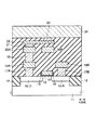
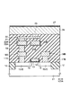
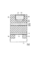
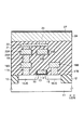
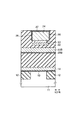
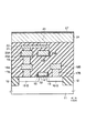
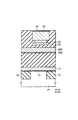
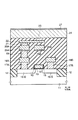
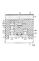
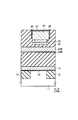
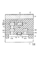
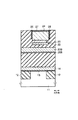
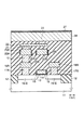
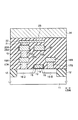
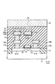
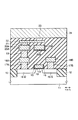
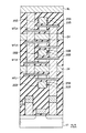
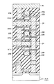
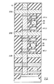
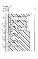
3. 実施例1
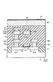
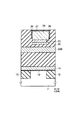
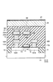
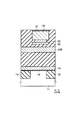
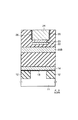
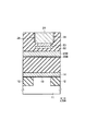
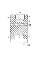
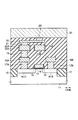
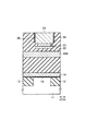
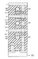
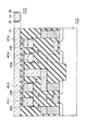
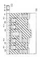
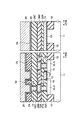
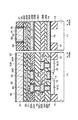
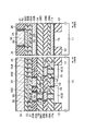
図7乃至図10は、本発明の磁気ランダムアクセスメモリの実施例1に関わるデバイス構造を示している。なお、図7及び図9は、Y方向の断面であり、図8は、図7のTMR素子部のX方向の断面であり、図10は、図9のTMR素子部のX方向の断面である。X方向とY方向は、互いに直交する。
【0098】
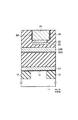
本例のデバイス構造の特徴は、TMR素子23の直下に配置される書き込みワード線20Bに関しては、その下面及び側面をヨーク材25Bで覆い、TMR素子23の直上に配置されるデータ選択線(読み出し/書き込みビット線)24に関しては、その上面及び側面をヨーク材26,27で覆った点にある。
【0099】
さらに、TMR素子23の直下に配置される書き込みワード線20Bの側面に配置されるヨーク材25Bに関しては、書き込み線20Bの上面よりも下部に窪んだ構造を有する点に特徴を有する。
【0100】
半導体基板(例えば、p型シリコン基板、p型ウェル領域など)11内には、STI( Shallow Trench Isolation )構造を有する素子分離絶縁層12が形成される。素子分離絶縁層12により取り囲まれた領域は、読み出し選択スイッチが形成される素子領域となる。
【0101】
本例のデバイス構造では、読み出し選択スイッチは、MOSトランジスタ(nチャネル型MOSトランジスタ)から構成される。半導体基板11上には、ゲート絶縁層13、ゲート電極14及び側壁絶縁層15が形成される。ゲート電極14は、X方向に延びており、読み出し動作時に、読み出しセル(TMR素子)を選択するための読み出しワード線として機能する。
【0102】
半導体基板11内には、ソース領域(例えば、n型拡散層)16−S及びドレイン領域(例えば、n型拡散層)16−Dが形成される。ゲート電極(読み出しワード線)14は、ソース領域16−Sとドレイン領域16−Dの間のチャネル領域上に配置される。
【0103】
第1金属配線層を構成する金属層のうちの1つは、複数のコンタクトプラグを縦に積み重ねるための中間層18Aとして機能し、他の1つは、ソース線18Bとして機能する。
【0104】
中間層18Aは、コンタクトプラグ17Aにより、読み出し選択スイッチ(MOSトランジスタ)のドレイン領域16−Dに電気的に接続される。ソース線18Bは、コンタクトプラグ17Bにより、読み出し選択スイッチのソース領域16−Sに電気的に接続される。ソース線18Bは、例えば、ゲート電極(読み出しワード線)14と同様に、X方向に延びている。
【0105】
第2金属配線層を構成する金属層のうちの1つは、複数のコンタクトプラグを縦に積み重ねるための中間層20Aとして機能し、他の1つは、書き込みワード線20Bとして機能する。中間層20Aは、コンタクトプラグ19により、中間層18Aに電気的に接続される。書き込みワード線20Bは、例えば、ゲート電極(読み出しワード線)14と同様に、X方向に延びている。
【0106】
本例のデバイス構造では、中間層20A及び書き込みワード線20Bの下面及び側面は、高い透磁率を有する材料、即ち、ヨーク材( yoke material )25A,25Bにより覆われている。ここで使用されるヨーク材25A,25Bは、導電性を有するものに限定される。
【0107】
また、中間層20A及び書き込みワード線20Bの側面に配置されるヨーク材25A,25Bに関しては、中間層20A及び書き込みワード線20Bの上面よりも下部に窪んでいる。つまり、ヨーク材25A,25BがTMR素子23に近付き過ぎることがないため、書き込みワード線20BとTMR素子23とが短絡する可能性を低くできる。
【0108】
なお、磁束は、高い透磁率を有する材料に集中する性質があるため、この高い透磁率を有する材料を磁力線の牽引役として使用すれば、書き込み動作時、書き込みワード線20Bに流れる書き込み電流により発生する磁界Hyを、TMR素子23に、効率よく、集中させることができる。
【0109】
本願の目的を達成するには、ヨーク材は、書き込みワード線20Bの下面及び側面を覆っていれば、十分である。但し、実際は、ヨーク材は、中間層20Aの下面及び側面にも形成される。これは、第2金属配線層としての中間層20A及び書き込みワード線20Bが同時に形成されることに起因する。
【0110】
第3金属配線層を構成する金属層のうちの1つは、TMR素子23の下部電極22として機能する。下部電極22は、コンタクトプラグ21により、中間層20Aに電気的に接続される。TMR素子23は、下部電極22上に搭載される。ここで、TMR素子23は、書き込みワード線20Bの直上に配置されると共に、X方向に長い長方形状(磁化容易軸がX方向)に形成される。
【0111】
第4金属配線層を構成する金属層のうちの1つは、データ選択線(読み出し/書き込みビット線)24として機能する。データ選択線24は、TMR素子23に電気的に接続されると共に、Y方向に延びている。
【0112】
本例のデバイス構造では、データ選択線24の上面及び側面は、高い透磁率を有する材料、即ち、ヨーク材26,27により覆われている。ここで使用されるヨーク材26,27としては、図7及び図8に示すように、導電性を有する材料から構成することができるし、また、図9及び図10に示すように、絶縁性を有する材料から構成することもできる。
【0113】
なお、磁束は、上述のように、高い透磁率を有する材料に集中する性質があるため、この高い透磁率を有する材料を磁力線の牽引役として使用すれば、書き込み動作時、データ選択線24に流れる書き込み電流により発生する磁界Hxを、TMR素子23に、効率よく、集中させることができる。
【0114】
TMR素子23の構造に関しては、特に、限定されない。図96に示すような構造であってもよいし、その他の構造であってもよい。また、TMR素子23は、複数ビットのデータを記憶できる多値記憶型であっても構わない。
【0115】
このようなデバイス構造においては、TMR素子23の直下に配置される書き込みワード線20Bに対しては、その下面及び側面にヨーク材25Bが形成される。また、TMR素子23の直上に配置されるデータ選択線(読み出し/書き込みビット線)24に対しては、その上面及び側面にヨーク材26,27が形成される。さらに、書き込みワード線20Bの側面のヨーク材25Bについては、書き込みワード線20Bの上面よりも下部に窪んでいる。
【0116】
従って、書き込みワード線20B及びデータ選択線24に流れる書き込み電流により発生する磁界を、効率よく、TMR素子23に印加することができる。
【0117】
なお、本例では、データ選択線24に対しては、その上面及び側面にヨーク材26,27を形成したが、これに限られず、以下のようにしても構わない。
【0118】
例えば、データ選択線24に対しては、図11乃至図14に示すように、その上面のみにヨーク材27を形成してもよいし、また、図15乃至図18に示すように、その側面のみにヨーク材26を形成してもよい。
【0119】
また、書き込みワード線20B及びヨーク材25Bは、ダマシンプロセス( damascene process )を採用して形成するのが好都合である。逆に言うと、書き込みワード線20B及びヨーク材25Bを、RIEプロセス( Reactive Ion Etching process )を採用して形成することは、プロセスが非常に複雑となるため、現実的に不可能となる。
【0120】
また、データ選択線24及びヨーク材26,27については、ダマシンプロセス及びRIEプロセスのいずれを採用してもよい。
【0121】
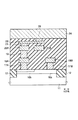
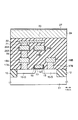
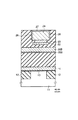
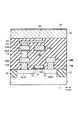
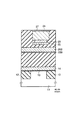
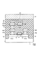
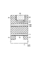
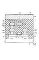
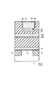
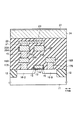
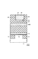
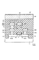
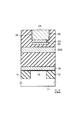
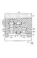
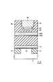
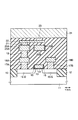
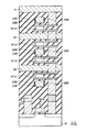
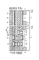
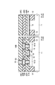
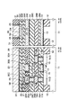
4. 実施例2
図19乃至図22は、本発明の磁気ランダムアクセスメモリの実施例2に関わるデバイス構造を示している。なお、図19及び図21は、Y方向の断面であり、図20は、図19のTMR素子部のX方向の断面であり、図22は、図21のTMR素子部のX方向の断面である。X方向とY方向は、互いに直交する。
【0122】
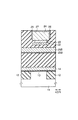
本例のデバイス構造の特徴は、TMR素子23の直下に配置される書き込みワード線20Bに関しては、その下面及び側面をヨーク材25Bで覆い、TMR素子23の直上に配置されるデータ選択線(読み出し/書き込みビット線)24に関しては、その上面及び側面をヨーク材26,27で覆った点にある。
【0123】
さらに、TMR素子23の直上に配置されるデータ選択線24の側面に配置されるヨーク材26に関しては、データ選択線24の下面よりも上部に窪んだ構造を有する点に特徴を有する。
【0124】
半導体基板(例えば、p型シリコン基板、p型ウェル領域など)11内には、STI( Shallow Trench Isolation )構造を有する素子分離絶縁層12が形成される。素子分離絶縁層12により取り囲まれた領域は、読み出し選択スイッチが形成される素子領域となる。
【0125】
本例のデバイス構造では、読み出し選択スイッチは、MOSトランジスタ(nチャネル型MOSトランジスタ)から構成される。半導体基板11上には、ゲート絶縁層13、ゲート電極14及び側壁絶縁層15が形成される。ゲート電極14は、X方向に延びており、読み出し動作時に、読み出しセル(TMR素子)を選択するための読み出しワード線として機能する。
【0126】
半導体基板11内には、ソース領域(例えば、n型拡散層)16−S及びドレイン領域(例えば、n型拡散層)16−Dが形成される。ゲート電極(読み出しワード線)14は、ソース領域16−Sとドレイン領域16−Dの間のチャネル領域上に配置される。
【0127】
第1金属配線層を構成する金属層のうちの1つは、複数のコンタクトプラグを縦に積み重ねるための中間層18Aとして機能し、他の1つは、ソース線18Bとして機能する。
【0128】
中間層18Aは、コンタクトプラグ17Aにより、読み出し選択スイッチ(MOSトランジスタ)のドレイン領域16−Dに電気的に接続される。ソース線18Bは、コンタクトプラグ17Bにより、読み出し選択スイッチのソース領域16−Sに電気的に接続される。ソース線18Bは、例えば、ゲート電極(読み出しワード線)14と同様に、X方向に延びている。
【0129】
第2金属配線層を構成する金属層のうちの1つは、複数のコンタクトプラグを縦に積み重ねるための中間層20Aとして機能し、他の1つは、書き込みワード線20Bとして機能する。中間層20Aは、コンタクトプラグ19により、中間層18Aに電気的に接続される。書き込みワード線20Bは、例えば、ゲート電極(読み出しワード線)14と同様に、X方向に延びている。
【0130】
本例のデバイス構造では、中間層20A及び書き込みワード線20Bの下面及び側面は、高い透磁率を有する材料、即ち、ヨーク材( yoke material )25A,25Bにより覆われている。ここで使用されるヨーク材25A,25Bは、導電性を有するものに限定される。
【0131】
なお、磁束は、高い透磁率を有する材料に集中する性質があるため、この高い透磁率を有する材料を磁力線の牽引役として使用すれば、書き込み動作時、書き込みワード線20Bに流れる書き込み電流により発生する磁界Hyを、TMR素子23に、効率よく、集中させることができる。
【0132】
本願の目的を達成するには、ヨーク材は、書き込みワード線20Bの下面及び側面を覆っていれば、十分である。但し、実際は、ヨーク材は、中間層20Aの下面及び側面にも形成される。これは、第2金属配線層としての中間層20A及び書き込みワード線20Bが同時に形成されることに起因する。
【0133】
第3金属配線層を構成する金属層のうちの1つは、TMR素子23の下部電極22として機能する。下部電極22は、コンタクトプラグ21により、中間層20Aに電気的に接続される。TMR素子23は、下部電極22上に搭載される。ここで、TMR素子23は、書き込みワード線20Bの直上に配置されると共に、X方向に長い長方形状(磁化容易軸がX方向)に形成される。
【0134】
第4金属配線層を構成する金属層のうちの1つは、データ選択線(読み出し/書き込みビット線)24として機能する。データ選択線24は、TMR素子23に電気的に接続されると共に、Y方向に延びている。
【0135】
本例のデバイス構造では、データ選択線24の上面及び側面は、高い透磁率を有する材料、即ち、ヨーク材26,27により覆われている。ここで使用されるヨーク材26,27としては、図19及び図20に示すように、導電性を有する材料から構成することができるし、また、図21及び図22に示すように、絶縁性を有する材料から構成することもできる。
【0136】
また、データ選択線24の側面に配置されるヨーク材26に関しては、データ選択線24の下面よりも上部に窪んでいる。つまり、ヨーク材26がTMR素子23に近付き過ぎることがない。
【0137】
なお、磁束は、上述のように、高い透磁率を有する材料に集中する性質があるため、この高い透磁率を有する材料を磁力線の牽引役として使用すれば、書き込み動作時、データ選択線24に流れる書き込み電流により発生する磁界Hxを、TMR素子23に、効率よく、集中させることができる。
【0138】
TMR素子23の構造に関しては、特に、限定されない。図96に示すような構造であってもよいし、その他の構造であってもよい。また、TMR素子23は、複数ビットのデータを記憶できる多値記憶型であっても構わない。
【0139】
このようなデバイス構造においては、TMR素子23の直下に配置される書き込みワード線20Bに対しては、その下面及び側面にヨーク材25Bが形成される。また、TMR素子23の直上に配置されるデータ選択線(読み出し/書き込みビット線)24に対しては、その上面及び側面にヨーク材26,27が形成される。さらに、データ選択線24の側面のヨーク材26については、データ選択線24の下面よりも上部に窪んでいる。
【0140】
従って、書き込みワード線20B及びデータ選択線24に流れる書き込み電流により発生する磁界を、効率よく、TMR素子23に印加することができる。
【0141】
なお、本例では、書き込みワード線20Bに対しては、その下面及び側面にヨーク材25Bを形成したが、これに限られず、以下のようにしても構わない。
【0142】
例えば、書き込みワード線20Bに対しては、図23乃至図26に示すように、その下面のみにヨーク材25Bを形成してもよいし、また、図27乃至図30に示すように、その側面のみにヨーク材25Bを形成してもよい。
【0143】
また、書き込みワード線20B及びヨーク材25Bは、ダマシンプロセス( damascene process )を採用して形成するのが好都合である。逆に言うと、書き込みワード線20B及びヨーク材25Bを、RIEプロセス( Reactive Ion Etching process )を採用して形成することは、プロセスが非常に複雑となるため、現実的に不可能となる。
【0144】
また、データ選択線24及びヨーク材26,27についても、ダマシンプロセスを採用して形成するのが好都合である。逆に言うと、データ選択線24及びヨーク材26,27を、RIEプロセスを採用して形成することは、プロセスが非常に複雑となるため、現実的に不可能となる。
【0145】
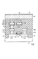
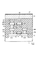
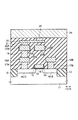
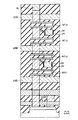
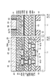
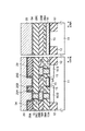
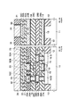
5. 実施例3
図31乃至図34は、本発明の磁気ランダムアクセスメモリの実施例3に関わるデバイス構造を示している。なお、図31及び図33は、Y方向の断面であり、図32は、図31のTMR素子部のX方向の断面であり、図34は、図33のTMR素子部のX方向の断面である。X方向とY方向は、互いに直交する。
【0146】
本例のデバイス構造の特徴は、TMR素子23の直下に配置される書き込みワード線20Bに関しては、その下面及び側面をヨーク材25Bで覆い、TMR素子23の直上に配置されるデータ選択線(読み出し/書き込みビット線)24に関しては、その上面及び側面をヨーク材26,27で覆った点にある。
【0147】
さらに、TMR素子23の直下に配置される書き込みワード線20Bの側面に配置されるヨーク材25Bに関しては、書き込み線20Bの上面よりも下部に窪んだ構造を有する点、また、TMR素子23の直上に配置されるデータ選択線24の側面に配置されるヨーク材26に関しては、データ選択線24の下面よりも上部に窪んだ構造を有する点に特徴を有する。
【0148】
半導体基板(例えば、p型シリコン基板、p型ウェル領域など)11内には、STI( Shallow Trench Isolation )構造を有する素子分離絶縁層12が形成される。素子分離絶縁層12により取り囲まれた領域は、読み出し選択スイッチが形成される素子領域となる。
【0149】
本例のデバイス構造では、読み出し選択スイッチは、MOSトランジスタ(nチャネル型MOSトランジスタ)から構成される。半導体基板11上には、ゲート絶縁層13、ゲート電極14及び側壁絶縁層15が形成される。ゲート電極14は、X方向に延びており、読み出し動作時に、読み出しセル(TMR素子)を選択するための読み出しワード線として機能する。
【0150】
半導体基板11内には、ソース領域(例えば、n型拡散層)16−S及びドレイン領域(例えば、n型拡散層)16−Dが形成される。ゲート電極(読み出しワード線)14は、ソース領域16−Sとドレイン領域16−Dの間のチャネル領域上に配置される。
【0151】
第1金属配線層を構成する金属層のうちの1つは、複数のコンタクトプラグを縦に積み重ねるための中間層18Aとして機能し、他の1つは、ソース線18Bとして機能する。
【0152】
中間層18Aは、コンタクトプラグ17Aにより、読み出し選択スイッチ(MOSトランジスタ)のドレイン領域16−Dに電気的に接続される。ソース線18Bは、コンタクトプラグ17Bにより、読み出し選択スイッチのソース領域16−Sに電気的に接続される。ソース線18Bは、例えば、ゲート電極(読み出しワード線)14と同様に、X方向に延びている。
【0153】
第2金属配線層を構成する金属層のうちの1つは、複数のコンタクトプラグを縦に積み重ねるための中間層20Aとして機能し、他の1つは、書き込みワード線20Bとして機能する。中間層20Aは、コンタクトプラグ19により、中間層18Aに電気的に接続される。書き込みワード線20Bは、例えば、ゲート電極(読み出しワード線)14と同様に、X方向に延びている。
【0154】
本例のデバイス構造では、中間層20A及び書き込みワード線20Bの下面及び側面は、高い透磁率を有する材料、即ち、ヨーク材( yoke material )25A,25Bにより覆われている。ここで使用されるヨーク材25A,25Bは、導電性を有するものに限定される。
【0155】
また、中間層20A及び書き込みワード線20Bの側面に配置されるヨーク材25A,25Bに関しては、中間層20A及び書き込みワード線20Bの上面よりも下部に窪んでいる。つまり、ヨーク材25A,25BがTMR素子23に近付き過ぎることがないため、書き込みワード線20BとTMR素子23とが短絡する可能性を低くできる。
【0156】
なお、磁束は、高い透磁率を有する材料に集中する性質があるため、この高い透磁率を有する材料を磁力線の牽引役として使用すれば、書き込み動作時、書き込みワード線20Bに流れる書き込み電流により発生する磁界Hyを、TMR素子23に、効率よく、集中させることができる。
【0157】
本願の目的を達成するには、ヨーク材は、書き込みワード線20Bの下面及び側面を覆っていれば、十分である。但し、実際は、ヨーク材は、中間層20Aの下面及び側面にも形成される。これは、第2金属配線層としての中間層20A及び書き込みワード線20Bが同時に形成されることに起因する。
【0158】
第3金属配線層を構成する金属層のうちの1つは、TMR素子23の下部電極22として機能する。下部電極22は、コンタクトプラグ21により、中間層20Aに電気的に接続される。TMR素子23は、下部電極22上に搭載される。ここで、TMR素子23は、書き込みワード線20Bの直上に配置されると共に、X方向に長い長方形状(磁化容易軸がX方向)に形成される。
【0159】
第4金属配線層を構成する金属層のうちの1つは、データ選択線(読み出し/書き込みビット線)24として機能する。データ選択線24は、TMR素子23に電気的に接続されると共に、Y方向に延びている。
【0160】
本例のデバイス構造では、データ選択線24の上面及び側面は、高い透磁率を有する材料、即ち、ヨーク材26,27により覆われている。ここで使用されるヨーク材26,27としては、図31及び図32に示すように、導電性を有する材料から構成することができるし、また、図33及び図34に示すように、絶縁性を有する材料から構成することもできる。
【0161】
また、データ選択線24の側面に配置されるヨーク材26に関しては、データ選択線24の下面よりも上部に窪んでいる。つまり、ヨーク材26がTMR素子23に近付き過ぎることがない。
【0162】
なお、磁束は、上述のように、高い透磁率を有する材料に集中する性質があるため、この高い透磁率を有する材料を磁力線の牽引役として使用すれば、書き込み動作時、データ選択線24に流れる書き込み電流により発生する磁界Hxを、TMR素子23に、効率よく、集中させることができる。
【0163】
TMR素子23の構造に関しては、特に、限定されない。図96に示すような構造であってもよいし、その他の構造であってもよい。また、TMR素子23は、複数ビットのデータを記憶できる多値記憶型であっても構わない。
【0164】
このようなデバイス構造においては、TMR素子23の直下に配置される書き込みワード線20Bに対しては、その下面及び側面にヨーク材25Bが形成される。また、TMR素子23の直上に配置されるデータ選択線(読み出し/書き込みビット線)24に対しては、その上面及び側面にヨーク材26,27が形成される。さらに、書き込みワード線20Bの側面のヨーク材25Bについては、書き込みワード線20Bの上面よりも下部に窪み、データ選択線24の側面のヨーク材26については、データ選択線24の下面よりも上部に窪んでいる。
【0165】
従って、書き込みワード線20B及びデータ選択線24に流れる書き込み電流により発生する磁界を、効率よく、TMR素子23に印加することができる。
【0166】
なお、書き込みワード線20B及びヨーク材25Bは、ダマシンプロセス( damascene process )を採用して形成するのが好都合である。逆に言うと、書き込みワード線20B及びヨーク材25Bを、RIEプロセス( Reactive Ion Etching process )を採用して形成することは、プロセスが非常に複雑となるため、現実的に不可能となる。
【0167】
また、データ選択線24及びヨーク材26,27についても、ダマシンプロセスを採用して形成するのが好都合である。逆に言うと、データ選択線24及びヨーク材26,27を、RIEプロセスを採用して形成することは、プロセスが非常に複雑となるため、現実的に不可能となる。
【0168】
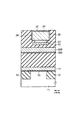
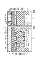
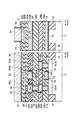
6. 実施例4
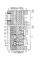
図35乃至図38は、本発明の磁気ランダムアクセスメモリの実施例4に関わるデバイス構造を示している。なお、図35及び図37は、Y方向の断面であり、図36は、図35のTMR素子部のX方向の断面であり、図38は、図37のTMR素子部のX方向の断面である。X方向とY方向は、互いに直交する。
【0169】
本例のデバイス構造の特徴は、TMR素子23の直下に配置される書き込みワード線20Bに関しては、その側面のみをヨーク材25Bで覆い、TMR素子23の直上に配置されるデータ選択線(読み出し/書き込みビット線)24に関しては、その上面及び側面をヨーク材26,27で覆った点にある。
【0170】
さらに、TMR素子23の直下に配置される書き込みワード線20Bの側面に配置されるヨーク材25Bに関しては、書き込み線20Bの上面よりも下部に窪んだ構造を有する点に特徴を有する。
【0171】
半導体基板(例えば、p型シリコン基板、p型ウェル領域など)11内には、STI( Shallow Trench Isolation )構造を有する素子分離絶縁層12が形成される。素子分離絶縁層12により取り囲まれた領域は、読み出し選択スイッチが形成される素子領域となる。
【0172】
本例のデバイス構造では、読み出し選択スイッチは、MOSトランジスタ(nチャネル型MOSトランジスタ)から構成される。半導体基板11上には、ゲート絶縁層13、ゲート電極14及び側壁絶縁層15が形成される。ゲート電極14は、X方向に延びており、読み出し動作時に、読み出しセル(TMR素子)を選択するための読み出しワード線として機能する。
【0173】
半導体基板11内には、ソース領域(例えば、n型拡散層)16−S及びドレイン領域(例えば、n型拡散層)16−Dが形成される。ゲート電極(読み出しワード線)14は、ソース領域16−Sとドレイン領域16−Dの間のチャネル領域上に配置される。
【0174】
第1金属配線層を構成する金属層のうちの1つは、複数のコンタクトプラグを縦に積み重ねるための中間層18Aとして機能し、他の1つは、ソース線18Bとして機能する。
【0175】
中間層18Aは、コンタクトプラグ17Aにより、読み出し選択スイッチ(MOSトランジスタ)のドレイン領域16−Dに電気的に接続される。ソース線18Bは、コンタクトプラグ17Bにより、読み出し選択スイッチのソース領域16−Sに電気的に接続される。ソース線18Bは、例えば、ゲート電極(読み出しワード線)14と同様に、X方向に延びている。
【0176】
第2金属配線層を構成する金属層のうちの1つは、複数のコンタクトプラグを縦に積み重ねるための中間層20Aとして機能し、他の1つは、書き込みワード線20Bとして機能する。中間層20Aは、コンタクトプラグ19により、中間層18Aに電気的に接続される。書き込みワード線20Bは、例えば、ゲート電極(読み出しワード線)14と同様に、X方向に延びている。
【0177】
本例のデバイス構造では、中間層20A及び書き込みワード線20Bの側面は、高い透磁率を有する材料、即ち、ヨーク材( yoke material )25A,25Bにより覆われている。ここで使用されるヨーク材25A,25Bは、図35及び図36に示すように、導電性を有する材料から構成することができるし、また、図37及び図38に示すように、絶縁性を有する材料から構成することもできる。
【0178】
また、中間層20A及び書き込みワード線20Bの側面に配置されるヨーク材25A,25Bに関しては、中間層20A及び書き込みワード線20Bの上面よりも下部に窪んでいる。つまり、ヨーク材25A,25BがTMR素子23に近付き過ぎることがないため、書き込みワード線20BとTMR素子23とが短絡する可能性を低くできる。
【0179】
なお、磁束は、高い透磁率を有する材料に集中する性質があるため、この高い透磁率を有する材料を磁力線の牽引役として使用すれば、書き込み動作時、書き込みワード線20Bに流れる書き込み電流により発生する磁界Hyを、TMR素子23に、効率よく、集中させることができる。
【0180】
本願の目的を達成するには、ヨーク材は、書き込みワード線20Bの側面を覆っていれば、十分である。但し、実際は、ヨーク材は、中間層20Aの側面にも形成される。これは、第2金属配線層としての中間層20A及び書き込みワード線20Bが同時に形成されることに起因する。
【0181】
第3金属配線層を構成する金属層のうちの1つは、TMR素子23の下部電極22として機能する。下部電極22は、コンタクトプラグ21により、中間層20Aに電気的に接続される。TMR素子23は、下部電極22上に搭載される。ここで、TMR素子23は、書き込みワード線20Bの直上に配置されると共に、X方向に長い長方形状(磁化容易軸がX方向)に形成される。
【0182】
第4金属配線層を構成する金属層のうちの1つは、データ選択線(読み出し/書き込みビット線)24として機能する。データ選択線24は、TMR素子23に電気的に接続されると共に、Y方向に延びている。
【0183】
本例のデバイス構造では、データ選択線24の上面及び側面は、高い透磁率を有する材料、即ち、ヨーク材26,27により覆われている。ここで使用されるヨーク材26,27としては、図35及び図36に示すように、導電性を有する材料から構成することができるし、また、図37及び図38に示すように、絶縁性を有する材料から構成することもできる。
【0184】
なお、磁束は、上述のように、高い透磁率を有する材料に集中する性質があるため、この高い透磁率を有する材料を磁力線の牽引役として使用すれば、書き込み動作時、データ選択線24に流れる書き込み電流により発生する磁界Hxを、TMR素子23に、効率よく、集中させることができる。
【0185】
TMR素子23の構造に関しては、特に、限定されない。図96に示すような構造であってもよいし、その他の構造であってもよい。また、TMR素子23は、複数ビットのデータを記憶できる多値記憶型であっても構わない。
【0186】
このようなデバイス構造においては、TMR素子23の直下に配置される書き込みワード線20Bに対しては、その側面にヨーク材25Bが形成される。また、TMR素子23の直上に配置されるデータ選択線(読み出し/書き込みビット線)24に対しては、その上面及び側面にヨーク材26,27が形成される。さらに、書き込みワード線20Bの側面のヨーク材25Bについては、書き込みワード線20Bの上面よりも下部に窪んでいる。
【0187】
従って、書き込みワード線20B及びデータ選択線24に流れる書き込み電流により発生する磁界を、効率よく、TMR素子23に印加することができる。
【0188】
なお、本例では、データ選択線24に対しては、その上面及び側面にヨーク材26,27を形成したが、これに限られず、以下のようにしても構わない。
【0189】
例えば、データ選択線24に対しては、図39乃至図42に示すように、その上面のみにヨーク材27を形成してもよいし、また、図43乃至図46に示すように、その側面のみにヨーク材26を形成してもよい。
【0190】
また、書き込みワード線20B及びヨーク材25Bは、ダマシンプロセス( damascene process )を採用して形成するのが好都合である。逆に言うと、書き込みワード線20B及びヨーク材25Bを、RIEプロセス( Reactive Ion Etching process )を採用して形成することは、プロセスが非常に複雑となるため、現実的に不可能となる。
【0191】
また、データ選択線24及びヨーク材26,27については、ダマシンプロセス及びRIEプロセスのいずれを採用してもよい。
【0192】
7. 実施例5
図47乃至図50は、本発明の磁気ランダムアクセスメモリの実施例5に関わるデバイス構造を示している。なお、図47及び図49は、Y方向の断面であり、図48は、図47のTMR素子部のX方向の断面であり、図50は、図49のTMR素子部のX方向の断面である。X方向とY方向は、互いに直交する。
【0193】
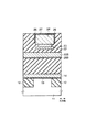
本例のデバイス構造の特徴は、TMR素子23の直下に配置される書き込みワード線20Bに関しては、その下面及び側面をヨーク材25Bで覆い、TMR素子23の直上に配置されるデータ選択線(読み出し/書き込みビット線)24に関しては、その側面のみをヨーク材26で覆った点にある。
【0194】
さらに、TMR素子23の直上に配置されるデータ選択線24の側面に配置されるヨーク材26に関しては、データ選択線24の下面よりも上部に窪んだ構造を有する点に特徴を有する。
【0195】
半導体基板(例えば、p型シリコン基板、p型ウェル領域など)11内には、STI( Shallow Trench Isolation )構造を有する素子分離絶縁層12が形成される。素子分離絶縁層12により取り囲まれた領域は、読み出し選択スイッチが形成される素子領域となる。
【0196】
本例のデバイス構造では、読み出し選択スイッチは、MOSトランジスタ(nチャネル型MOSトランジスタ)から構成される。半導体基板11上には、ゲート絶縁層13、ゲート電極14及び側壁絶縁層15が形成される。ゲート電極14は、X方向に延びており、読み出し動作時に、読み出しセル(TMR素子)を選択するための読み出しワード線として機能する。
【0197】
半導体基板11内には、ソース領域(例えば、n型拡散層)16−S及びドレイン領域(例えば、n型拡散層)16−Dが形成される。ゲート電極(読み出しワード線)14は、ソース領域16−Sとドレイン領域16−Dの間のチャネル領域上に配置される。
【0198】
第1金属配線層を構成する金属層のうちの1つは、複数のコンタクトプラグを縦に積み重ねるための中間層18Aとして機能し、他の1つは、ソース線18Bとして機能する。
【0199】
中間層18Aは、コンタクトプラグ17Aにより、読み出し選択スイッチ(MOSトランジスタ)のドレイン領域16−Dに電気的に接続される。ソース線18Bは、コンタクトプラグ17Bにより、読み出し選択スイッチのソース領域16−Sに電気的に接続される。ソース線18Bは、例えば、ゲート電極(読み出しワード線)14と同様に、X方向に延びている。
【0200】
第2金属配線層を構成する金属層のうちの1つは、複数のコンタクトプラグを縦に積み重ねるための中間層20Aとして機能し、他の1つは、書き込みワード線20Bとして機能する。中間層20Aは、コンタクトプラグ19により、中間層18Aに電気的に接続される。書き込みワード線20Bは、例えば、ゲート電極(読み出しワード線)14と同様に、X方向に延びている。
【0201】
本例のデバイス構造では、中間層20A及び書き込みワード線20Bの下面及び側面は、高い透磁率を有する材料、即ち、ヨーク材( yoke material )25A,25Bにより覆われている。ここで使用されるヨーク材25A,25Bは、導電性を有するものに限定される。
【0202】
なお、磁束は、高い透磁率を有する材料に集中する性質があるため、この高い透磁率を有する材料を磁力線の牽引役として使用すれば、書き込み動作時、書き込みワード線20Bに流れる書き込み電流により発生する磁界Hyを、TMR素子23に、効率よく、集中させることができる。
【0203】
本願の目的を達成するには、ヨーク材は、書き込みワード線20Bの下面及び側面を覆っていれば、十分である。但し、実際は、ヨーク材は、中間層20Aの下面及び側面にも形成される。これは、第2金属配線層としての中間層20A及び書き込みワード線20Bが同時に形成されることに起因する。
【0204】
第3金属配線層を構成する金属層のうちの1つは、TMR素子23の下部電極22として機能する。下部電極22は、コンタクトプラグ21により、中間層20Aに電気的に接続される。TMR素子23は、下部電極22上に搭載される。ここで、TMR素子23は、書き込みワード線20Bの直上に配置されると共に、X方向に長い長方形状(磁化容易軸がX方向)に形成される。
【0205】
第4金属配線層を構成する金属層のうちの1つは、データ選択線(読み出し/書き込みビット線)24として機能する。データ選択線24は、TMR素子23に電気的に接続されると共に、Y方向に延びている。
【0206】
本例のデバイス構造では、データ選択線24の側面は、高い透磁率を有する材料、即ち、ヨーク材26により覆われている。ここで使用されるヨーク材26としては、図47及び図48に示すように、導電性を有する材料から構成することができるし、また、図49及び図50に示すように、絶縁性を有する材料から構成することもできる。
【0207】
また、データ選択線24の側面に配置されるヨーク材26に関しては、データ選択線24の下面よりも上部に窪んでいる。つまり、ヨーク材26がTMR素子23に近付き過ぎることがない。
【0208】
なお、磁束は、上述のように、高い透磁率を有する材料に集中する性質があるため、この高い透磁率を有する材料を磁力線の牽引役として使用すれば、書き込み動作時、データ選択線24に流れる書き込み電流により発生する磁界Hxを、TMR素子23に、効率よく、集中させることができる。
【0209】
TMR素子23の構造に関しては、特に、限定されない。図96に示すような構造であってもよいし、その他の構造であってもよい。また、TMR素子23は、複数ビットのデータを記憶できる多値記憶型であっても構わない。
【0210】
このようなデバイス構造においては、TMR素子23の直下に配置される書き込みワード線20Bに対しては、その下面及び側面にヨーク材25Bが形成される。また、TMR素子23の直上に配置されるデータ選択線(読み出し/書き込みビット線)24に対しては、その側面のみにヨーク材26が形成される。さらに、データ選択線24の側面のヨーク材26については、データ選択線24の下面よりも上部に窪んでいる。
【0211】
従って、書き込みワード線20B及びデータ選択線24に流れる書き込み電流により発生する磁界を、効率よく、TMR素子23に印加することができる。
【0212】
なお、本例では、書き込みワード線20Bに対しては、その下面及び側面にヨーク材25Bを形成したが、これに限られず、以下のようにしても構わない。
【0213】
例えば、書き込みワード線20Bに対しては、図51乃至図54に示すように、その下面のみにヨーク材25Bを形成してもよいし、また、図55乃至図58に示すように、その側面のみにヨーク材25Bを形成してもよい。
【0214】
また、書き込みワード線20B及びヨーク材25Bは、ダマシンプロセス( damascene process )を採用して形成するのが好都合である。逆に言うと、書き込みワード線20B及びヨーク材25Bを、RIEプロセス( Reactive Ion Etching process )を採用して形成することは、プロセスが非常に複雑となるため、現実的に不可能となる。
【0215】
また、データ選択線24及びヨーク材26についても、ダマシンプロセスを採用して形成するのが好都合である。逆に言うと、データ選択線24及びヨーク材26を、RIEプロセスを採用して形成することは、プロセスが非常に複雑となるため、現実的に不可能となる。
【0216】
8. 実施例6
図59乃至図62は、本発明の磁気ランダムアクセスメモリの実施例6に関わるデバイス構造を示している。なお、図59及び図61は、Y方向の断面であり、図60は、図59のTMR素子部のX方向の断面であり、図62は、図61のTMR素子部のX方向の断面である。X方向とY方向は、互いに直交する。
【0217】
本例のデバイス構造の特徴は、TMR素子23の直下に配置される書き込みワード線20Bに関しては、その側面のみをヨーク材25Bで覆い、TMR素子23の直上に配置されるデータ選択線(読み出し/書き込みビット線)24に関しては、その側面のみをヨーク材26で覆った点にある。
【0218】
さらに、TMR素子23の直下に配置される書き込みワード線20Bの側面に配置されるヨーク材25Bに関しては、書き込み線20Bの上面よりも下部に窪んだ構造を有する点、また、TMR素子23の直上に配置されるデータ選択線24の側面に配置されるヨーク材26に関しては、データ選択線24の下面よりも上部に窪んだ構造を有する点に特徴を有する。
【0219】
半導体基板(例えば、p型シリコン基板、p型ウェル領域など)11内には、STI( Shallow Trench Isolation )構造を有する素子分離絶縁層12が形成される。素子分離絶縁層12により取り囲まれた領域は、読み出し選択スイッチが形成される素子領域となる。
【0220】
本例のデバイス構造では、読み出し選択スイッチは、MOSトランジスタ(nチャネル型MOSトランジスタ)から構成される。半導体基板11上には、ゲート絶縁層13、ゲート電極14及び側壁絶縁層15が形成される。ゲート電極14は、X方向に延びており、読み出し動作時に、読み出しセル(TMR素子)を選択するための読み出しワード線として機能する。
【0221】
半導体基板11内には、ソース領域(例えば、n型拡散層)16−S及びドレイン領域(例えば、n型拡散層)16−Dが形成される。ゲート電極(読み出しワード線)14は、ソース領域16−Sとドレイン領域16−Dの間のチャネル領域上に配置される。
【0222】
第1金属配線層を構成する金属層のうちの1つは、複数のコンタクトプラグを縦に積み重ねるための中間層18Aとして機能し、他の1つは、ソース線18Bとして機能する。
【0223】
中間層18Aは、コンタクトプラグ17Aにより、読み出し選択スイッチ(MOSトランジスタ)のドレイン領域16−Dに電気的に接続される。ソース線18Bは、コンタクトプラグ17Bにより、読み出し選択スイッチのソース領域16−Sに電気的に接続される。ソース線18Bは、例えば、ゲート電極(読み出しワード線)14と同様に、X方向に延びている。
【0224】
第2金属配線層を構成する金属層のうちの1つは、複数のコンタクトプラグを縦に積み重ねるための中間層20Aとして機能し、他の1つは、書き込みワード線20Bとして機能する。中間層20Aは、コンタクトプラグ19により、中間層18Aに電気的に接続される。書き込みワード線20Bは、例えば、ゲート電極(読み出しワード線)14と同様に、X方向に延びている。
【0225】
本例のデバイス構造では、中間層20A及び書き込みワード線20Bの側面は、高い透磁率を有する材料、即ち、ヨーク材( yoke material )25A,25Bにより覆われている。ここで使用されるヨーク材25A,25Bは、図59及び図60に示すように、導電性を有する材料から構成することができるし、また、図61及び図62に示すように、絶縁性を有する材料から構成することもできる。
【0226】
また、中間層20A及び書き込みワード線20Bの側面に配置されるヨーク材25A,25Bに関しては、中間層20A及び書き込みワード線20Bの上面よりも下部に窪んでいる。つまり、ヨーク材25A,25BがTMR素子23に近付き過ぎることがないため、書き込みワード線20BとTMR素子23とが短絡する可能性を低くできる。
【0227】
なお、磁束は、高い透磁率を有する材料に集中する性質があるため、この高い透磁率を有する材料を磁力線の牽引役として使用すれば、書き込み動作時、書き込みワード線20Bに流れる書き込み電流により発生する磁界Hyを、TMR素子23に、効率よく、集中させることができる。
【0228】
本願の目的を達成するには、ヨーク材は、書き込みワード線20Bの側面を覆っていれば、十分である。但し、実際は、ヨーク材は、中間層20Aの側面にも形成される。これは、第2金属配線層としての中間層20A及び書き込みワード線20Bが同時に形成されることに起因する。
【0229】
第3金属配線層を構成する金属層のうちの1つは、TMR素子23の下部電極22として機能する。下部電極22は、コンタクトプラグ21により、中間層20Aに電気的に接続される。TMR素子23は、下部電極22上に搭載される。ここで、TMR素子23は、書き込みワード線20Bの直上に配置されると共に、X方向に長い長方形状(磁化容易軸がX方向)に形成される。
【0230】
第4金属配線層を構成する金属層のうちの1つは、データ選択線(読み出し/書き込みビット線)24として機能する。データ選択線24は、TMR素子23に電気的に接続されると共に、Y方向に延びている。
【0231】
本例のデバイス構造では、データ選択線24の側面は、高い透磁率を有する材料、即ち、ヨーク材26により覆われている。ここで使用されるヨーク材26としては、図59及び図60に示すように、導電性を有する材料から構成することができるし、また、図61及び図62に示すように、絶縁性を有する材料から構成することもできる。
【0232】
また、データ選択線24の側面に配置されるヨーク材26に関しては、データ選択線24の下面よりも上部に窪んでいる。つまり、ヨーク材26がTMR素子23に近付き過ぎることがない。
【0233】
なお、磁束は、上述のように、高い透磁率を有する材料に集中する性質があるため、この高い透磁率を有する材料を磁力線の牽引役として使用すれば、書き込み動作時、データ選択線24に流れる書き込み電流により発生する磁界Hxを、TMR素子23に、効率よく、集中させることができる。
【0234】
TMR素子23の構造に関しては、特に、限定されない。図96に示すような構造であってもよいし、その他の構造であってもよい。また、TMR素子23は、複数ビットのデータを記憶できる多値記憶型であっても構わない。
【0235】
このようなデバイス構造においては、TMR素子23の直下に配置される書き込みワード線20Bに対しては、その側面のみにヨーク材25Bが形成される。また、TMR素子23の直上に配置されるデータ選択線(読み出し/書き込みビット線)24に対しては、その側面のみにヨーク材26が形成される。さらに、書き込みワード線20Bの側面のヨーク材25Bについては、書き込みワード線20Bの上面よりも下部に窪み、データ選択線24の側面のヨーク材26については、データ選択線24の下面よりも上部に窪んでいる。
【0236】
従って、書き込みワード線20B及びデータ選択線24に流れる書き込み電流により発生する磁界を、効率よく、TMR素子23に印加することができる。
【0237】
なお、書き込みワード線20B及びヨーク材25Bは、ダマシンプロセス( damascene process )を採用して形成するのが好都合である。逆に言うと、書き込みワード線20B及びヨーク材25Bを、RIEプロセス( Reactive Ion Etching process )を採用して形成することは、プロセスが非常に複雑となるため、現実的に不可能となる。
【0238】
また、データ選択線24及びヨーク材26についても、ダマシンプロセスを採用して形成するのが好都合である。逆に言うと、データ選択線24及びヨーク材26を、RIEプロセスを採用して形成することは、プロセスが非常に複雑となるため、現実的に不可能となる。
【0239】
9. 実施例7〜12
次に、実施例4〜6に関わるデバイス構造の改良例としての実施例7〜12について説明する。
【0240】
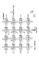
これら実施例7〜12のデバイス構造の特徴は、TMR素子を複数段に積み重ねた場合(実施例7〜10)又は複数個のTMR素子を横方向に並べた場合(実施例11,12)に、複数のTMR素子で1つの書き込み線を共有し、かつ、その書き込み線の側面を高透磁率を有するヨーク材で覆った点にある。
【0241】
(1) 実施例7
図63及び図64は、本発明の磁気ランダムアクセスメモリの実施例7に関わるデバイス構造を示している。
【0242】
本例のデバイス構造では、半導体基板11上に、2つのTMR素子23が積み重ねられており、これら2つのTMR素子23は、1つのデータ選択線(読み出し/書き込みビット線)24を共有している。
【0243】
データ選択線24は、2つのTMR素子の間に配置され、Y方向に延びている。また、1つのTMR素子23は、データ選択線24の下面に接触し、他の1つのTMR素子23は、データ選択線24の上面に接触している。データ選択線24の側面は、高透磁率を有するヨーク材26により覆われている。
【0244】
ヨーク材26は、データ選択線24の上面よりも下部に窪み、かつ、データ選択線24の下面よりも上部に窪んでいる。
【0245】
書き込み動作時には、データ選択線24に書き込み電流が流れる。この書き込み電流により発生した磁界は、ヨーク材26により、効率よく、TMR素子23に印加される。
【0246】
TMR素子23の直下又は直上には、Y方向に直交するX方向に延びる書き込みワード線20Bが配置される。書き込みワード線20Bの側面は、高透磁率を有するヨーク材25Bにより覆われている。
【0247】
ヨーク材25Bは、書き込みワード線20Bの上面よりも下部に窪み、かつ、書き込みワード線20Bの下面よりも上部に窪んでいる。
【0248】
書き込み動作時には、書き込みワード線20Bに書き込み電流が流れる。この書き込み電流により発生した磁界は、ヨーク材25Bにより、効率よく、TMR素子23に印加される。
【0249】
なお、ヨーク材25B,26は、図63に示すように、導電材から構成されていてもよいし、図64に示すように、絶縁材から構成されていてもよい。
【0250】
(2) 実施例8
図65及び図66は、本発明の磁気ランダムアクセスメモリの実施例8に関わるデバイス構造を示している。
【0251】
本例のデバイス構造では、半導体基板11上に、4つのTMR素子23が積み重ねられている。これらTMR素子23のうちの2つは、1つの書き込みワード線20B、又は、1つのデータ選択線(読み出し/書き込みビット線)24を共有している。
【0252】
データ選択線24は、2つのTMR素子23の間に配置され、Y方向に延びている。また、1つのTMR素子23は、データ選択線24の下面に接触し、他の1つのTMR素子23は、データ選択線24の上面に接触している。データ選択線24の側面は、高透磁率を有するヨーク材26により覆われている。
【0253】
ヨーク材26は、データ選択線24の上面よりも下部に窪み、かつ、データ選択線24の下面よりも上部に窪んでいる。
【0254】
書き込み動作時には、データ選択線24に書き込み電流が流れる。この書き込み電流により発生した磁界は、ヨーク材26により、効率よく、TMR素子23に印加される。
【0255】
上段のデータ選択線24の下面に接触しているTMR素子23と下段のデータ選択線24の上面に接触しているTMR素子23との間には、Y方向に直交するX方向に延びる1つの書き込みワード線20Bが配置される。この書き込みワード線20Bは、これら2つのTMR素子に共有される。書き込みワード線20Bの側面は、高透磁率を有するヨーク材25Bにより覆われている。
【0256】
また、上段のデータ選択線24の上面に接触しているTMR素子23の直上及び下段のデータ選択線24の下面に接触しているTMR素子23の直下には、それぞれ、X方向に延びる書き込みワード線20Bが配置される。書き込みワード線20Bの側面は、高透磁率を有するヨーク材25Bにより覆われている。
【0257】
ヨーク材25Bは、書き込みワード線20Bの上面よりも下部に窪み、かつ、書き込みワード線20Bの下面よりも上部に窪んでいる。
【0258】
書き込み動作時には、書き込みワード線20Bに書き込み電流が流れる。この書き込み電流により発生した磁界は、ヨーク材25Bにより、効率よく、TMR素子23に印加される。
【0259】
なお、ヨーク材25B,26は、図65に示すように、導電材から構成されていてもよいし、図66に示すように、絶縁材から構成されていてもよい。
【0260】
(3) 実施例9
図67乃至図70は、本発明の磁気ランダムアクセスメモリの実施例9に関わるデバイス構造を示している。
【0261】
本例のデバイス構造では、半導体基板11上に、直列接続された4つのTMR素子23が積み重ねられている。これら直列接続されたTMR素子23の一端は、読み出し選択スイッチRSWに接続され、他端は、読み出しビット線BLに接続される。これらTMR素子23のうちの2つは、1つの書き込みワード線20B、又は、1つの書き込みビット線24を共有している。
【0262】
書き込みビット線24は、2つのTMR素子23の間に配置され、Y方向に延びている。書き込みビット線24の側面は、高透磁率を有するヨーク材26により覆われている。ヨーク材26は、書き込みビット線24の上面よりも下部に窪み、かつ、書き込みビット線24の下面よりも上部に窪んでいる。
【0263】
書き込み動作時には、書き込みビット線24に書き込み電流が流れる。この書き込み電流により発生した磁界は、ヨーク材26により、効率よく、TMR素子23に印加される。
【0264】
書き込みワード線20Bは、2つのTMR素子23の間に配置され、Y方向に直交するX方向に延びている。書き込みワード線20Bの側面は、高透磁率を有するヨーク材25Bにより覆われている。また、書き込みワード線20Bは、TMR素子23の直下又は直上に配置され、X方向に延びている。書き込みワード線20Bの側面は、高透磁率を有するヨーク材25Bにより覆われている。
【0265】
ヨーク材25Bは、書き込みワード線20Bの上面よりも下部に窪み、かつ、書き込みワード線20Bの下面よりも上部に窪んでいる。
【0266】
書き込み動作時には、書き込みワード線20Bに書き込み電流が流れる。この書き込み電流により発生した磁界は、ヨーク材25Bにより、効率よく、TMR素子23に印加される。
【0267】
なお、ヨーク材25B,26は、図67及び図68に示すように、導電材から構成されていてもよいし、図69及び図70に示すように、絶縁材から構成されていてもよい。
【0268】
(4) 実施例10
図71乃至図74は、本発明の磁気ランダムアクセスメモリの実施例10に関わるデバイス構造を示している。
【0269】
本例のデバイス構造では、半導体基板11上に、並列接続された4つのTMR素子23が積み重ねられている。これら並列接続されたTMR素子23の一端は、読み出し選択スイッチRSWに接続され、他端は、読み出しビット線BLに接続される。これらTMR素子23のうちの2つは、1つの書き込みワード線20B、又は、1つの書き込みビット線24を共有している。
【0270】
書き込みビット線24は、2つのTMR素子23の間に配置され、Y方向に延びている。書き込みビット線24の側面は、高透磁率を有するヨーク材26により覆われている。ヨーク材26は、書き込みビット線24の上面よりも下部に窪み、かつ、書き込みビット線24の下面よりも上部に窪んでいる。
【0271】
書き込み動作時には、書き込みビット線24に書き込み電流が流れる。この書き込み電流により発生した磁界は、ヨーク材26により、効率よく、TMR素子23に印加される。
【0272】
書き込みワード線20Bは、2つのTMR素子23の間に配置され、Y方向に直交するX方向に延びている。書き込みワード線20Bの側面は、高透磁率を有するヨーク材25Bにより覆われている。また、書き込みワード線20Bは、TMR素子23の直下又は直上に配置され、X方向に延びている。書き込みワード線20Bの側面は、高透磁率を有するヨーク材25Bにより覆われている。
【0273】
ヨーク材25Bは、書き込みワード線20Bの上面よりも下部に窪み、かつ、書き込みワード線20Bの下面よりも上部に窪んでいる。
【0274】
書き込み動作時には、書き込みワード線20Bに書き込み電流が流れる。この書き込み電流により発生した磁界は、ヨーク材25Bにより、効率よく、TMR素子23に印加される。
【0275】
なお、ヨーク材25B,26は、図71及び図72に示すように、導電材から構成されていてもよいし、図73及び図74に示すように、絶縁材から構成されていてもよい。
【0276】
(5) 実施例11
図75及び図76は、本発明の磁気ランダムアクセスメモリの実施例11に関わるデバイス構造を示している。
【0277】
本例のデバイス構造では、半導体基板11上において、横方向(半導体基板の表面に平行な方向)に複数(本例では、4つ)のTMR素子23が配置されている。これらTMR素子23の一端は、読み出し選択スイッチRSWに共通に接続され、他端は、データ選択線(読み出し/書き込みビット線)24に共通に接続される。これらTMR素子23は、1つのデータ選択線(読み出し/書き込みビット線)24を共有している。
【0278】
データ選択線24は、複数のTMR素子23の直上に配置され、Y方向に延びている。データ選択線24の側面は、高透磁率を有するヨーク材26により覆われている。ヨーク材26は、データ選択線24の下面よりも上部に窪んでいる。書き込み動作時には、データ選択線24に書き込み電流が流れる。この書き込み電流により発生した磁界は、ヨーク材26により、効率よく、TMR素子23に印加される。
【0279】
書き込みワード線20Bは、TMR素子23の直下に配置され、Y方向に直交するX方向に延びている。書き込みワード線20Bの側面は、高透磁率を有するヨーク材25Bにより覆われている。ヨーク材25Bは、書き込みワード線20Bの上面よりも下部に窪んでいる。
【0280】
書き込み動作時には、書き込みワード線20Bに書き込み電流が流れる。この書き込み電流により発生した磁界は、ヨーク材25Bにより、効率よく、TMR素子23に印加される。
【0281】
なお、ヨーク材25B,26は、図75に示すように、導電材から構成されていてもよいし、図76に示すように、絶縁材から構成されていてもよい。
【0282】
(6) 実施例12
図77及び図78は、本発明の磁気ランダムアクセスメモリの実施例12に関わるデバイス構造を示している。
【0283】
本例のデバイス構造では、半導体基板11上において、横方向(半導体基板の表面に平行な方向)に複数(本例では、4つ)のTMR素子23が配置されている。これらTMR素子23の一端は、読み出し選択スイッチRSWに共通に接続され、他端は、それぞれ独立に、データ選択線(読み出しビット線/書き込みワード線)20Bに接続される。
【0284】
これらTMR素子23は、1つの書き込みビット線24を共有している。書き込みビット線24は、複数のTMR素子23の直上に配置され、Y方向に延びている。書き込みビット線24の側面は、高透磁率を有するヨーク材26により覆われている。ヨーク材26は、データ選択線24の下面よりも上部に窪んでいる。書き込み動作時には、書き込みビット線24に書き込み電流が流れる。この書き込み電流により発生した磁界は、ヨーク材26により、効率よく、TMR素子23に印加される。
【0285】
データ選択線20Bは、TMR素子23の直下に配置され、Y方向に直交するX方向に延びている。データ選択線20Bの側面は、高透磁率を有するヨーク材25Bにより覆われている。ヨーク材25Bは、書き込みワード線20Bの上面よりも下部に窪んでいる。
【0286】
書き込み動作時には、データ選択線20Bに書き込み電流が流れる。この書き込み電流により発生した磁界は、ヨーク材25Bにより、効率よく、TMR素子23に印加される。
【0287】
なお、ヨーク材25B,26は、図77に示すように、導電材から構成されていてもよいし、図78に示すように、絶縁材から構成されていてもよい。
【0288】
10. メモリセルアレイ構造
参考例1,2及び実施例1〜12に関わるデバイス構造により実現されるメモリセルアレイ構造(回路構造)の例について説明する。
【0289】
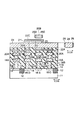
図79は、磁気ランダムアクセスメモリのメモリセルアレイ構造の主要部を示している。
【0290】
このセルアレイ構造は、TMR素子の磁化容易軸がY方向を向いていることを前提とするため、書き込みワード線に流れる書き込み電流の向きが、書き込みデータに応じて変化する。
【0291】
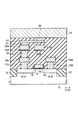
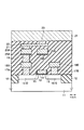
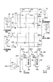
制御信号φ1,φ31,φ32,φ33は、NチャネルMOSトランジスタQN1,QN31,QN32,QN33のオン/オフを制御して、データ選択線(読み出し/書き込みビット線)BL1,BL2,BL3に電流を流すか否かを決定する。データ選択線BL1,BL2,BL3の一端(NチャネルMOSトランジスタQN1側)には、電流駆動電源40が接続される。電流駆動電源40は、データ選択線BL1,BL2,BL3の一端の電位をVyにする。
【0292】
NチャネルMOSトランジスタQN31,QN32,QN33は、データ選択線BL1,BL2,BL3の他端と接地点Vssとの間に接続される。
【0293】
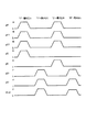
書き込み動作時においては、制御信号φ1が“H”レベルとなり、かつ、制御信号φ31,φ32,φ33のうちの1つが“H”レベルとなる。例えば、メモリセルMC1のTMR素子に対してデータ書き込みを行う場合には、図80のタイミングチャートに示すように、制御信号φ1,φ31が“H”レベルとなるため、データ選択線BL1に電流が流れる。この時、制御信号φ41,φ42,φ43は、“L”レベルとなっている。
【0294】
また、Vx1は、“1”−書き込みのための電流駆動電源電位であり、Vx2は、“0”−書き込みのための電流駆動電源電位である。
【0295】
例えば、“1”−書き込み時には、図80に示すように、制御信号φ5,φ11が“H”レベルになる。この時、制御信号φ6,φ12は、“L”レベルとなっている。このため、書き込みワード線WWL1には、左から右(電流駆動電源41から接地点)に向かって電流が流れる。従って、データ選択線BL1と書き込みワード線WWL1の交点に配置されるメモリセルMC1のTMR素子に“1”−データが書き込まれる。
【0296】
また、“0”−書き込み時には、図80に示すように、制御信号φ6,φ11が“H”レベルになる。この時、制御信号φ5,φ12は、“L”レベルとなっている。このため、書き込みワード線WWL1には、右から左(接地点Vssから電流駆動電源42)に向かって電流が流れる。従って、データ選択線BL1と書き込みワード線WWL1の交点に配置されるメモリセルMC1のTMR素子に“0”−データが書き込まれる。
【0297】
このように、書き込み動作時において、制御信号φ1は、全てのデータ選択線に駆動電流を供給するために用いられ、制御信号φ31,φ32,φ33は、駆動電流を流すデータ選択線を選択するために用いられる。なお、本例では、データ選択線に流れる駆動電流の向きは、一定である。制御信号φ5,φ6は、書き込みワード線に流れる電流の向き(書き込みデータに対応)を制御するために用いられ、制御信号φ11,φ12は、駆動電流を流す書き込みワード線を選択するために用いられる。
【0298】
本例では、説明を簡単にするため、3×2のメモリセルアレイを前提としている。書き込みワード線WWL1,WWL2とデータ選択線BL1,BL2,BL3の交点には、それぞれ、メモリセル(TMR素子)が配置される。ここで、メモリセルMC1に記憶されたデータを読み出すためには、制御信号φ21,φ22,φ41,φ42,φ43を、以下のように制御する。
【0299】
即ち、読み出し動作時には、読み出しワード線RWL1に与える制御信号φ21を“H”レベルにし、読み出しワード線RWL1に繋がるNチャネルMOSトランジスタをオン状態とする。この時、他の読み出しワード線RWL2に与える制御信号φ22は、“L”レベルとなっている。
【0300】
また、制御信号φ41を“H”レベルとし、他の制御信号φ42,φ43を“L”レベルとすると、読み出し電源43から、メモリセルMC1(NチャネルMOSトランジスタ及びTMR素子)、データ選択線BL1、NチャネルMOSトランジスタQN41及び検出抵抗Rsを経由して、接地点に向かって、駆動電流が流れる。
【0301】
このため、検出抵抗Rsの両端には、メモリセルMC1のデータ値に応じた検出電圧Voが発生する。この検出電圧Voを、例えば、センスアンプS/Aにより検出することにより、メモリセル(TMR素子)のデータを読み出すことができる。
【0302】
11. 製造方法
次に、参考例1,2及び実施例1〜12に関わるデバイス構造のうち、主なものについて、その製造方法を詳細に説明する。
【0303】
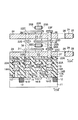
(1) 実施例3に関わるデバイス構造の製造方法
まず、図81に示すように、PEP( Photo Engraving Process )法、CVD( Chemical Vapour Deposition )法、CMP( Chemical Mechanical Polishing )法などの周知の方法を用いて、半導体基板11内に、STI構造の素子分離絶縁層12を形成する。
【0304】
また、素子分離絶縁層12に取り囲まれた素子領域内に、読み出し選択スイッチとしてのMOSトランジスタを形成する。
【0305】
MOSトランジスタは、CVD法、PEP法及びRIE( Reactive Ion Etching )法により、ゲート絶縁層13及びゲート電極(読み出しワード線)14を形成した後、イオン注入法により、ソース領域16−S及びドレイン領域16−Dを形成することにより、容易に形成できる。なお、ゲート電極14の側壁部には、CVD法及びRIE法により、側壁絶縁層15を形成してもよい。
【0306】
この後、CVD法により、MOSトランジスタを完全に覆う絶縁層28Aを形成する。また、CMP法を用いて、絶縁層28Aの表面を平坦化する。PEP法及びRIE法を用いて、絶縁層28A内に、MOSトランジスタのソース拡散層16−S及びドレイン拡散層16−Dに達するコンタクトホールを形成する。
【0307】
スパッタ法により、絶縁層28A上及びコンタクトホールの内面上に、バリアメタル(例えば、Ta(15nm)とTaN(15nm)の積層)51を形成する。続けて、絶縁層28A上に、コンタクトホールを完全に満たす導電材(例えば、不純物を含む導電性ポリシリコン膜、金属膜など)を形成する。そして、CMP法により、導電材及びバリアメタル51を研磨し、コンタクトプラグ17A,17Bを形成する。
【0308】
CVD法を用いて、絶縁層28A上に、絶縁層28Bを形成する。PEP法及びRIE法を用いて、絶縁層28B内に、配線溝を形成する。スパッタ法により、絶縁層28B上及び配線溝の内面上に、バリアメタル(例えば、TaとTaNの積層)52を形成する。続けて、スパッタ法により、絶縁層28B上に、配線溝を完全に満たす導電材(例えば、アルミニウム、銅などの金属膜)を形成する。この後、CMPにより、導電材及びバリアメタル52を研磨し、中間層18A及びソース線18Bを形成する。
【0309】
続けて、CVD法を用いて、絶縁層28B上に、絶縁層28Cを形成する。PEP法及びRIE法を用いて、絶縁層28C内に、バイアホール(via hole)を形成する。スパッタ法により、絶縁層28C上及びバイアホールの内面上に、バリアメタル(例えば、TaとTaNの積層)53を形成する。続けて、スパッタ法により、絶縁層28C上に、バイアホールを完全に満たす導電材(例えば、アルミニウム、銅などの金属膜)を形成する。この後、CMP法により、導電材及びバリアメタル53を研磨し、バイアプラグ19を形成する。
【0310】
次に、図82に示すように、CVD法を用いて、絶縁層28C上に、絶縁層29を形成する。PEP法及びRIE法を用いて、絶縁層29内に、配線溝を形成する。スパッタ法を用いて、絶縁層29上及び配線溝内に、高透磁率を有するヨーク材(例えば、NiFe)25を、約20nmの厚さで形成する。
【0311】
また、スパッタ法により、絶縁層28C上及びバイアホールの内面上に、バリアメタル(例えば、TaとTaNの積層)54を形成する。続けて、スパッタ法を用いて、配線溝を完全に満たす導電材(例えば、アルミニウム、銅、又は、これらの合金(AlCu)など)20を形成する。
【0312】
なお、導電材を銅(Cu)から構成する場合、この導電層は、例えば、まず、80nm程度のCuシード層を形成した後に、メッキ法により、Cuシード層上に、十分に厚い(例えば、約800nm)Cu層を積み重ねる、という方法で形成することができる。
【0313】
この後、CMPにより、導電材20及びバリアメタル54を研磨すると、中間層20A及び書き込みワード線20Bが形成される(図83を参照)。
【0314】
本例では、図83に示すように、導電材20A,20Bを配線溝内のみに残した後、図82のヨーク材25をエッチング又はCMP法により研磨する。ヨーク材25A,25Bは、その上面が、絶縁層29の上面(又は導電材20A,20Bの上面)よりも下部に配置されるような条件で研磨される。このような工程を経ることにより、書き込みワード線20Bの上面よりも下部に窪んだヨーク材25Bが形成される。
【0315】
次に、図83に示すように、CVD法を用いて、絶縁層29上に、絶縁層30Aを形成する。PEP法及びRIE法を用いて、絶縁層30A内に、バイアホールを形成する。スパッタ法により、絶縁層30A上及びバイアホールの内面上に、バリアメタル(例えば、TaN(10nm))55を形成する。続けて、CVD法により、絶縁層30A上に、バイアホールを完全に満たす導電材(例えば、タングステンなどの金属膜)を形成する。この後、CMP法により、導電材及びバリアメタル55を研磨し、バイアプラグ21を形成する。
【0316】
ここで、絶縁層30Aの厚さ(又はバイアプラグ21の高さ)は、書き込みワード線20BとTMR素子23との距離を決定する。磁界の強さは、距離に反比例して減少していくため、TMR素子を書き込みワード線20Bにできるだけ近づけ、小さな駆動電流によりデータの書き換えが行えるようにすることが望ましい。よって、絶縁層30Aの厚さは、できるだけ薄くする。
【0317】
CVD法を用いて、絶縁層30A上に、絶縁層30Bを形成する。PEP法及びRIE法を用いて、絶縁層30B内に、配線溝を形成する。スパッタ法により、絶縁層30B上に、配線溝を完全に満たす導電材(例えば、Taなどの金属膜)を、約50nmの厚さで形成する。この後、CMPにより導電材を研磨し、ローカルインターコネクト線(TMR素子の下部電極)22を形成する。
【0318】
スパッタ法を用いて、ローカルインターコネクト線22上に、例えば、NiFe(約5nm)、IrMn(約12nm)、CoFe(約3nm)、AlOx(約1.2nm)、CoFe(約5nm)及びNiFe(約15nm)を、順次、形成する。この後、これら積層膜をパターニングし、TMR素子23を形成する。
【0319】
また、CVD法を用いて、TMR素子23を覆う絶縁層30Cを形成した後、例えば、CMP法によりTMR素子23上の絶縁層30Cを除去し、この絶縁層30CがTMR素子23の側面のみを覆うようにする。
【0320】
次に、図84に示すように、CVD法を用いて、絶縁層30C上に、絶縁層31を形成する。PEP法及びRIE法を用いて、TMR素子23上の絶縁層31に配線溝を形成する。
【0321】
CVD法及びRIE法を用いて、絶縁層31の配線溝の側壁部に、絶縁層31とは異なる絶縁層50を形成する。この後、スパッタ法により、絶縁31上及び配線溝の内面上に、バリアメタル(例えば、Ti(25nm)とTiN(25nm)の積層)56を形成する。続けて、スパッタ法により、絶縁層31上に、配線溝を完全に満たす導電材(例えば、AlCu(650nm))を形成する。そして、CMPにより、導電材及びバリアメタル56を研磨し、データ選択線(読み出し/書き込みビット線)24を形成する。
【0322】
次に、図85に示すように、RIE法などのエッチング方法を用いて、絶縁層50のみを選択的にエッチングする。絶縁層50は、データ選択線24の下面近傍のみに残存させる。この後、CVD法を用いて、絶縁層50が除去された部分を満たすようなヨーク材(例えば、NiFe)26を、約50nmの厚さで形成する。このヨーク材26は、データ選択線24上及び絶縁層31上にも形成される。
【0323】
次に、図86に示すように、PEP法及びRIE法を用いて、ヨーク材26をパターニングする。その結果、ヨーク材26は、データ選択線24の上面及び側面を覆い、かつ、データ選択線24の下面よりも上部に窪んだ構造となる。
【0324】
以上の工程により、実施例3(図15及び図16)に関わる磁気ランダムアクセスメモリが完成する。
【0325】
なお、本例の製造方法では、金属配線20A,20B,24は、ダマシンプロセスにより形成されたが、例えば、RIEプロセスにより、金属配線20A,20B,24を形成することも可能である。
【0326】
また、本例の製造方法では、ヨーク材25A,25Bを形成した後にバリアメタル54を形成したが、これに代えて、例えば、バリアメタル54を形成した後にヨーク材25A,25Bを形成してもよい。
【0327】
(2) 実施例6に関わるデバイス構造の製造方法
まず、図87に示すように、PEP( Photo Engraving Process )法、CVD( Chemical Vapour Deposition )法、CMP( Chemical Mechanical Polishing )法などの周知の方法を用いて、半導体基板11内に、STI構造の素子分離絶縁層12を形成する。
【0328】
また、素子分離絶縁層12に取り囲まれた素子領域内に、読み出し選択スイッチとしてのMOSトランジスタを形成する。
【0329】
MOSトランジスタは、CVD法、PEP法及びRIE( Reactive Ion Etching )法により、ゲート絶縁層13及びゲート電極(読み出しワード線)14を形成した後、イオン注入法により、ソース領域16−S及びドレイン領域16−Dを形成することにより、容易に形成できる。なお、ゲート電極14の側壁部には、CVD法及びRIE法により、側壁絶縁層15を形成してもよい。
【0330】
この後、CVD法により、MOSトランジスタを完全に覆う絶縁層28Aを形成する。また、CMP法を用いて、絶縁層28Aの表面を平坦化する。PEP法及びRIE法を用いて、絶縁層28A内に、MOSトランジスタのソース拡散層16−S及びドレイン拡散層16−Dに達するコンタクトホールを形成する。
【0331】
スパッタ法により、絶縁層28A上及びコンタクトホールの内面上に、バリアメタル(例えば、Ta(15nm)とTaN(15nm)の積層)51を形成する。続けて、絶縁層28A上に、コンタクトホールを完全に満たす導電材(例えば、不純物を含む導電性ポリシリコン膜、金属膜など)を形成する。そして、CMP法により、導電材及びバリアメタル51を研磨し、コンタクトプラグ17A,17Bを形成する。
【0332】
CVD法を用いて、絶縁層28A上に、絶縁層28Bを形成する。PEP法及びRIE法を用いて、絶縁層28B内に、配線溝を形成する。スパッタ法により、絶縁層28B上及び配線溝の内面上に、バリアメタル(例えば、TaとTaNの積層)52を形成する。続けて、スパッタ法により、絶縁層28B上に、配線溝を完全に満たす導電材(例えば、アルミニウム、銅などの金属膜)を形成する。この後、CMPにより、導電材及びバリアメタル52を研磨し、中間層18A及びソース線18Bを形成する。
【0333】
続けて、CVD法を用いて、絶縁層28B上に、絶縁層28Cを形成する。PEP法及びRIE法を用いて、絶縁層28C内に、バイアホール(via hole)を形成する。スパッタ法により、絶縁層28C上及びバイアホールの内面上に、バリアメタル(例えば、TaとTaNの積層)53を形成する。続けて、スパッタ法により、絶縁層28C上に、バイアホールを完全に満たす導電材(例えば、アルミニウム、銅などの金属膜)を形成する。この後、CMP法により、導電材及びバリアメタル53を研磨し、バイアプラグ19を形成する。
【0334】
次に、図88に示すように、CVD法を用いて、絶縁層28C上に、絶縁層29を形成する。PEP法及びRIE法を用いて、絶縁層29内に、配線溝を形成する。スパッタ法を用いて、絶縁層29上及び配線溝内に、高透磁率を有するヨーク材(例えば、NiFe)25A,25Bを、約20nmの厚さで形成する。この後、RIE法を用いて、ヨーク材25A,25Bをエッチングすると、このヨーク材25A,25Bは、配線溝の側壁部のみに残存する。
【0335】
スパッタ法により、絶縁層29上及び配線溝の内面上に、バリアメタル(例えば、TaとTaNの積層)54を形成する。続けて、スパッタ法を用いて、絶縁層29上に、配線溝を完全に満たす導電材(例えば、アルミニウム、銅などの金属膜)20を形成する。この後、CMPにより、導電材20及びバリアメタル54を研磨すると、中間層20A及び書き込みワード線20Bが形成される(図89を参照)。
【0336】
ここで、本例では、図89に示すように、導電材20A,20Bを配線溝内のみに残した後、ヨーク材25A,25Bをエッチング又はCMP法により研磨する。ヨーク材25A,25Bは、その上面が、絶縁層29の上面(又は導電材20A,20Bの上面)よりも下部に配置されるような条件で研磨される。このような工程を経ることにより、書き込みワード線20Bの上面よりも下部に窪んだヨーク材25Bが形成される。
【0337】
次に、図89に示すように、CVD法を用いて、絶縁層29上に、絶縁層30Aを形成する。PEP法及びRIE法を用いて、絶縁層30A内に、バイアホールを形成する。スパッタ法により、絶縁層30A上及びバイアホールの内面上に、バリアメタル(例えば、TaとTaNの積層)55を形成する。続けて、CVD法により、絶縁層30A上に、バイアホールを完全に満たす導電材(例えば、タングステンなどの金属膜)を形成する。この後、CMP法により、導電材及びバリアメタル55を研磨し、バイアプラグ21を形成する。
【0338】
ここで、絶縁層30Aの厚さ(又はバイアプラグ21の高さ)は、書き込みワード線20BとTMR素子23との距離を決定する。磁界の強さは、距離に反比例して減少していくため、TMR素子を書き込みワード線20Bにできるだけ近づけ、小さな駆動電流によりデータの書き換えが行えるようにすることが望ましい。よって、絶縁層30Aの厚さは、できるだけ薄くする。
【0339】
CVD法を用いて、絶縁層30A上に、絶縁層30Bを形成する。PEP法及びRIE法を用いて、絶縁層30B内に、配線溝を形成する。スパッタ法により、絶縁層30B上に、配線溝を完全に満たす導電材(例えば、Taなどの金属膜)を形成する。この後、CMPにより導電材を研磨し、ローカルインターコネクト線(TMR素子の下部電極)22を形成する。
【0340】
CVD法を用いて、ローカルインターコネクト線22上に、例えば、NiFe(約5nm)、IrMn(約12nm)、CoFe(約3nm)、AlOx(約1.2nm)、CoFe(約5nm)及びNiFe(約15nm)を、順次、形成する。この後、これら積層膜をパターニングし、TMR素子23を形成する。
【0341】
また、CVD法を用いて、TMR素子23を覆う絶縁層30Cを形成した後、例えば、CMP法によりTMR素子23上の絶縁層30Cを除去し、この絶縁層30CがTMR素子23の側面のみを覆うようにする。
【0342】
次に、図90に示すように、CVD法を用いて、絶縁層30C上に、絶縁層31を形成する。PEP法及びRIE法を用いて、TMR素子23上の絶縁層31に配線溝を形成する。
【0343】
CVD法及びRIE法を用いて、絶縁層31の配線溝の側壁部に、絶縁層31とは異なる絶縁層50を形成する。この後、スパッタ法により、絶縁層31上及び配線溝の内面上に、バリアメタル(例えば、Ti(25nm)とTiN(25nm)の積層)56を形成する。続けて、スパッタ法により、絶縁層31上に、配線溝を完全に満たす導電材(例えば、AlCu(650nm))を形成する。そして、CMPにより、導電材及びバリアメタル56を研磨し、データ選択線(読み出し/書き込みビット線)24を形成する。
【0344】
次に、図91に示すように、RIE法などのエッチング方法を用いて、絶縁層50のみを選択的にエッチングする。絶縁層50は、データ選択線24の下面近傍のみに残存させる。この後、CVD法を用いて、絶縁層50が除去された部分を満たすようなヨーク材26を形成する。このヨーク材26は、データ選択線24上及び絶縁層31上にも形成される。
【0345】
次に、図92に示すように、CMP法又はRIE法を用いて、ヨーク材26をエッチングする。その結果、データ選択線24上及び絶縁層31上のヨーク材26は、除去され、ヨーク材26は、データ選択線24の側面のみを覆い、かつ、データ選択線24の下面よりも上部に窪んだ構造となる。
【0346】
以上の工程により、実施例6(図59及び図60)に関わる磁気ランダムアクセスメモリが完成する。
【0347】
なお、本例の製造方法では、金属配線20A,20B,24は、ダマシンプロセスにより形成されたが、例えば、RIEプロセスにより、金属配線20A,20B,24を形成することも可能である。
【0348】
また、本例の製造方法では、ヨーク材25A,25Bを形成した後にバリアメタル54を形成したが、これに代えて、例えば、バリアメタル54を形成した後にヨーク材25A,25Bを形成してもよい。
【0349】
ところで、データ選択線24の側面を覆うヨーク材26については、以下に示すような方法で形成することもできる。
【0350】
まず、図93に示すように、CVD法を用いて、絶縁層30C上に、絶縁層31を形成する。PEP法及びRIE法を用いて、TMR素子23上の絶縁層31に配線溝を形成する。この後、スパッタ法により、絶縁層31上及び配線溝の内面上に、バリアメタル(例えば、Ti(25nm)とTiN(25nm)の積層)56を形成する。続けて、スパッタ法により、絶縁層31上に、配線溝を完全に満たす導電材(例えば、AlCu(650nm))を形成する。そして、CMPにより、導電材及びバリアメタル56を研磨し、データ選択線(読み出し/書き込みビット線)24を形成する。
【0351】
次に、図94に示すように、RIE法などのエッチング方法を用いて、絶縁層31のみを選択的にエッチングする。絶縁層31は、データ選択線24の下面近傍のみに残存させる。
【0352】
次に、図95に示すように、CVD法を用いて、絶縁層31上並びにデータ選択線24の側面上及び上面上に、ヨーク材(例えば、NiFe)26を、約50nmの厚さで形成する。そして、RIE法により、このヨーク材26をエッチングすると、データ選択線24上及び絶縁層31上のヨーク材26は、除去され、ヨーク材26は、データ選択線24の側面のみを覆い、かつ、データ選択線24の下面よりも上部に窪んだ構造となる。
【0353】
以上の工程により、実施例6(図59及び図60)に関わる磁気ランダムアクセスメモリが完成する。
【0354】
12. その他
参考例1,2及び実施例1−6並びに製造方法の説明においては、1つのTMR素子と1つの読み出し選択スイッチ(MOSトランジスタ)によりメモリセルが構成され、書き込みワード線とデータ選択線(読み出し/書き込みビット線)を有する磁気ランダムアクセスメモリを例に説明した。
【0355】
しかし、本発明は、当然に、このようなセルアレイ構造の磁気ランダムアクセスメモリに限定されるものではなく、例えば、実施例7−12にも示したように、それらのデバイス構造も含めて、全ての磁気ランダムアクセスメモリに適用可能である。
【0356】
例えば、読み出し選択スイッチを有しない磁気ランダムアクセスメモリ、読み出しビット線と書き込みビットを別々に設けた磁気ランダムアクセスメモリ、1つのTMR素子に複数ビットを記憶させるようにした磁気ランダムアクセスメモリなどにも適用できる。
【0357】
【発明の効果】
以上、説明したように、本発明の磁気ランダムアクセスメモリによれば、書き込みワード線及び書き込みビット線の表面の一部に、高透磁率を有するヨーク材を設け、かつ、そのヨーク材をTMR素子側に対し反対側に窪ませたことにより、書き込みワード線とTMR素子との短絡の可能性を低くでき、書き込み動作時、合成磁界を、効率よく、TMR素子に作用させることができる。
【図面の簡単な説明】
【図1】本発明の磁気ランダムアクセスメモリの参考例1を示す断面図。
【図2】本発明の磁気ランダムアクセスメモリの参考例1を示す断面図。
【図3】本発明の磁気ランダムアクセスメモリの参考例2を示す断面図。
【図4】本発明の磁気ランダムアクセスメモリの参考例2を示す断面図。
【図5】本発明の磁気ランダムアクセスメモリの参考例2を示す断面図。
【図6】本発明の磁気ランダムアクセスメモリの参考例2を示す断面図。
【図7】本発明の磁気ランダムアクセスメモリの実施例1を示す断面図。
【図8】本発明の磁気ランダムアクセスメモリの実施例1を示す断面図。
【図9】本発明の磁気ランダムアクセスメモリの実施例1を示す断面図。
【図10】本発明の磁気ランダムアクセスメモリの実施例1を示す断面図。
【図11】実施例1の変形例を示す断面図。
【図12】実施例1の変形例を示す断面図。
【図13】実施例1の変形例を示す断面図。
【図14】実施例1の変形例を示す断面図。
【図15】実施例1の変形例を示す断面図。
【図16】実施例1の変形例を示す断面図。
【図17】実施例1の変形例を示す断面図。
【図18】実施例1の変形例を示す断面図。
【図19】本発明の磁気ランダムアクセスメモリの実施例2を示す断面図。
【図20】本発明の磁気ランダムアクセスメモリの実施例2を示す断面図。
【図21】本発明の磁気ランダムアクセスメモリの実施例2を示す断面図。
【図22】本発明の磁気ランダムアクセスメモリの実施例2を示す断面図。
【図23】実施例2の変形例を示す断面図。
【図24】実施例2の変形例を示す断面図。
【図25】実施例2の変形例を示す断面図。
【図26】実施例2の変形例を示す断面図。
【図27】実施例2の変形例を示す断面図。
【図28】実施例2の変形例を示す断面図。
【図29】実施例2の変形例を示す断面図。
【図30】実施例2の変形例を示す断面図。
【図31】本発明の磁気ランダムアクセスメモリの実施例3を示す断面図。
【図32】本発明の磁気ランダムアクセスメモリの実施例3を示す断面図。
【図33】本発明の磁気ランダムアクセスメモリの実施例3を示す断面図。
【図34】本発明の磁気ランダムアクセスメモリの実施例3を示す断面図。
【図35】本発明の磁気ランダムアクセスメモリの実施例4を示す断面図。
【図36】本発明の磁気ランダムアクセスメモリの実施例4を示す断面図。
【図37】本発明の磁気ランダムアクセスメモリの実施例4を示す断面図。
【図38】本発明の磁気ランダムアクセスメモリの実施例4を示す断面図。
【図39】実施例4の変形例を示す断面図。
【図40】実施例4の変形例を示す断面図。
【図41】実施例4の変形例を示す断面図。
【図42】実施例4の変形例を示す断面図。
【図43】実施例4の変形例を示す断面図。
【図44】実施例4の変形例を示す断面図。
【図45】実施例4の変形例を示す断面図。
【図46】実施例4の変形例を示す断面図。
【図47】本発明の磁気ランダムアクセスメモリの実施例5を示す断面図。
【図48】本発明の磁気ランダムアクセスメモリの実施例5を示す断面図。
【図49】本発明の磁気ランダムアクセスメモリの実施例5を示す断面図。
【図50】本発明の磁気ランダムアクセスメモリの実施例5を示す断面図。
【図51】実施例5の変形例を示す断面図。
【図52】実施例5の変形例を示す断面図。
【図53】実施例5の変形例を示す断面図。
【図54】実施例5の変形例を示す断面図。
【図55】実施例5の変形例を示す断面図。
【図56】実施例5の変形例を示す断面図。
【図57】実施例5の変形例を示す断面図。
【図58】実施例5の変形例を示す断面図。
【図59】本発明の磁気ランダムアクセスメモリの実施例6を示す断面図。
【図60】本発明の磁気ランダムアクセスメモリの実施例6を示す断面図。
【図61】本発明の磁気ランダムアクセスメモリの実施例6を示す断面図。
【図62】本発明の磁気ランダムアクセスメモリの実施例6を示す断面図。
【図63】本発明の磁気ランダムアクセスメモリの実施例7を示す断面図。
【図64】本発明の磁気ランダムアクセスメモリの実施例7を示す断面図。
【図65】本発明の磁気ランダムアクセスメモリの実施例8を示す断面図。
【図66】本発明の磁気ランダムアクセスメモリの実施例8を示す断面図。
【図67】本発明の磁気ランダムアクセスメモリの実施例9を示す断面図。
【図68】本発明の磁気ランダムアクセスメモリの実施例9を示す断面図。
【図69】本発明の磁気ランダムアクセスメモリの実施例9を示す断面図。
【図70】本発明の磁気ランダムアクセスメモリの実施例9を示す断面図。
【図71】本発明の磁気ランダムアクセスメモリの実施例10を示す断面図。
【図72】本発明の磁気ランダムアクセスメモリの実施例10を示す断面図。
【図73】本発明の磁気ランダムアクセスメモリの実施例10を示す断面図。
【図74】本発明の磁気ランダムアクセスメモリの実施例10を示す断面図。
【図75】本発明の磁気ランダムアクセスメモリの実施例11を示す断面図。
【図76】本発明の磁気ランダムアクセスメモリの実施例11を示す断面図。
【図77】本発明の磁気ランダムアクセスメモリの実施例12を示す断面図。
【図78】本発明の磁気ランダムアクセスメモリの実施例12を示す断面図。
【図79】本発明の磁気ランダムアクセスメモリのセルアレイの構造例を示す回路図。
【図80】図79のセルアレイの動作波形を示す図。
【図81】実施例3のデバイス構造の製造方法の一工程を示す断面図。
【図82】実施例3のデバイス構造の製造方法の一工程を示す断面図。
【図83】実施例3のデバイス構造の製造方法の一工程を示す断面図。
【図84】実施例3のデバイス構造の製造方法の一工程を示す断面図。
【図85】実施例3のデバイス構造の製造方法の一工程を示す断面図。
【図86】実施例3のデバイス構造の製造方法の一工程を示す断面図。
【図87】実施例6のデバイス構造の製造方法の一工程を示す断面図。
【図88】実施例6のデバイス構造の製造方法の一工程を示す断面図。
【図89】実施例6のデバイス構造の製造方法の一工程を示す断面図。
【図90】実施例6のデバイス構造の製造方法の一工程を示す断面図。
【図91】実施例6のデバイス構造の製造方法の一工程を示す断面図。
【図92】実施例6のデバイス構造の製造方法の一工程を示す断面図。
【図93】実施例6のデバイス構造の製造方法の一工程を示す断面図。
【図94】実施例6のデバイス構造の製造方法の一工程を示す断面図。
【図95】実施例6のデバイス構造の製造方法の一工程を示す断面図。
【図96】TMR素子の構造例を示す図。
【図97】TMR素子の2つの状態を示す図。
【図98】磁気ランダムアクセスメモリの書き込み動作原理を示す図。
【図99】TMR曲線を示す図。
【図100】アステロイド曲線を示す図。
【符号の説明】
11 :半導体基板、
12 :素子分離絶縁層、
13 :ゲート絶縁層、
14 :ゲート電極(読み出しワード線)、
15 :側壁絶縁層、
16−S :ソース領域、
16−D :ドレイン領域、
17A,17B :コンタクトプラグ、
18A,20A :中間層、
18B :ソース線(読み出しワード線)、
19,21 :バイアプラグ、
20B :書き込みワード線、
22 :下部電極、
23 :TMR素子、
24 :データ選択線(読み出し/書き込みビット線)、
25,25A,25B,26,27 :ヨーク材、
28A〜28C,29,30A〜30C,31,50 :絶縁層、
40,41,42 :電流駆動電源、
43 :読み出し電源、
44 :検出回路。[0001]
BACKGROUND OF THE INVENTION
The present invention relates to a magnetic random access memory (MRAM) in which a memory cell is configured using a TMR element that stores “1”, “0” -information by a tunneling magnetoresistive effect. About.
[0002]
[Prior art]
In recent years, many memories that store information based on a new principle have been proposed, one of which is the tunneling magnetoresistive (Tunneling Magneto Resistive: TMR) proposed by Roy Scheuerlein et.al. .) There is a memory using the effect (for example, see ISSCC2000 Technical Digest p.128 “A 10ns Read and Write Non-Volatile Memory Array Using a Magnetic Tunnel Junction and FET Switch in each Cell”).
[0003]
The magnetic random access memory stores “1”, “0” -information by the TMR element. As shown in FIG. 96, the TMR element has a structure in which an insulating layer (tunnel barrier) is sandwiched between two magnetic layers (ferromagnetic layers). Information stored in the TMR element is determined by whether the spin directions of the two magnetic layers are parallel or antiparallel.
[0004]
Here, as shown in FIG. 97, parallel means that the spin directions (magnetization directions) of the two magnetic layers are the same, and antiparallel means that the spin directions of the two magnetic layers are the same. It means that the direction is opposite (the direction of the arrow indicates the direction of the spin).
[0005]
Normally, an antiferromagnetic layer is disposed on one side of the two magnetic layers. The antiferromagnetic layer is a member for easily rewriting information by fixing the spin direction of the magnetic layer on one side and changing only the spin direction on the other side.
[0006]
A magnetic layer whose spin direction is fixed is called a fixed layer or a pinned layer. A magnetic layer whose spin direction can be freely changed according to write data is called a free layer or a storage layer.
[0007]
As shown in FIG. 97, when the spin directions of the two magnetic layers are parallel, the tunnel resistance of the insulating layer (tunnel barrier) sandwiched between these two magnetic layers is the lowest. This state is “1” -state. When the spin directions of the two magnetic layers are antiparallel, the tunnel resistance of the insulating layer (tunnel barrier) sandwiched between these two magnetic layers is the highest. This state is a “0” -state.
[0008]
Next, the write operation principle for the TMR element will be briefly described with reference to FIG.
[0009]
The TMR element is arranged at an intersection of a write word line and a data selection line (read / write bit line) that intersect each other. Writing is achieved by passing a current through the write word line and the data selection line and making the spin direction of the TMR element parallel or anti-parallel using a magnetic field generated by the current flowing through both wirings.
[0010]
For example, when the easy axis of the TMR element is in the X direction, the write word line extends in the X direction, and the data selection line extends in the Y direction orthogonal to the X direction, the write word line is unidirectional during writing. A current flowing in one direction or the other direction is caused to flow in the data selection line in accordance with write data.
[0011]
When a current flowing in one direction is applied to the data selection line, the spin direction of the TMR element is parallel ("1" -state). On the other hand, when a current flowing in the other direction is passed through the data selection line, the spin direction of the TMR element is antiparallel ("0" -state).
[0012]
The mechanism for changing the spin direction of the TMR element is as follows.
[0013]
As shown in the TMR curve of FIG. 99, when a magnetic field Hx is applied in the long-side (Easy-Axis) direction of the TMR element, the resistance value of the TMR element changes by about 17%, for example. This rate of change, that is, the ratio of resistance values before and after the change is called the MR ratio.
[0014]
Note that the MR ratio varies depending on the properties of the magnetic layer. At present, a TMR element having an MR ratio of about 50% is also obtained.
[0015]
The TMR element is subjected to a combined magnetic field of a magnetic field Hx in the Easy-Axis direction and a magnetic field Hy in the Hard-Axis direction. As indicated by the solid line in FIG. 100, the magnitude of the magnetic field Hx in the Easy-Axis direction required to change the resistance value of the TMR element also changes depending on the magnitude of the magnetic field Hy in the Hard-Axis direction. By utilizing this phenomenon, data can be written only to the TMR element existing at the intersection of the selected write word line and the selected data selection line among the memory cells arranged in an array.
[0016]
This state will be further described using the asteroid curve in FIG.
The asteroid curve of the TMR element is, for example, as shown by the solid line in FIG. That is, if the magnitude of the combined magnetic field of the magnetic field Hx in the Easy-Axis direction and the magnetic field Hy in the Hard-Axis direction is outside the asteroid curve (solid line) (for example, the position of the black circle), the spin direction of the magnetic layer Can be reversed.
[0017]
Conversely, if the magnitude of the combined magnetic field of the magnetic field Hx in the Easy-Axis direction and the magnetic field Hy in the Hard-Axis direction is inside the asteroid curve (solid line) (for example, the position of the white circle), The direction of the spin cannot be reversed.
[0018]
Therefore, data is written to the TMR element by changing the magnitude of the magnetic field Hx in the Easy-Axis direction and the magnitude of the magnetic field Hy in the Hard-Axis direction and changing the position of the synthesized magnetic field in the Hx-Hy plane. Can be controlled.
[0019]
Reading can be easily performed by passing a current through the selected TMR element and detecting the resistance value of the TMR element.
[0020]
For example, a switch element is connected in series to the TMR element, and only the switch element connected to the selected read word line is turned on to create a current path. As a result, a current flows only in the selected TMR element, so that data of the TMR element can be read.
[0021]
[Problems to be solved by the invention]
In the magnetic random access memory, as described above, in the data write, a write current is supplied to the write word line and the data selection line (read / write bit line), and the resultant magnetic field is applied to the TMR element. By doing.
[0022]
Therefore, in order to efficiently perform data writing, it is important to efficiently apply this synthesized magnetic field to the TMR element. If the combined magnetic field is efficiently applied to the TMR element, the reliability of the write operation can be improved, the write current can be reduced, and the power consumption can be reduced.
[0023]
However, a device structure effective for causing a combined magnetic field generated by a write current flowing in each of a write word line and a data selection line to efficiently act on a TMR element has not been sufficiently studied. That is, such a device structure actually needs to be examined from the viewpoint of the manufacturing process of whether or not it can be easily manufactured as well as the combined magnetic field is efficiently applied to the TMR element.
[0024]
The present invention has been made to solve such a problem, and an object of the present invention is to provide a device structure capable of efficiently applying a combined magnetic field to a TMR element during a write operation in a magnetic random access memory. The manufacturing method is proposed.
[0025]
[Means for Solving the Problems]
(1) (1) A magnetic random access memory according to the present invention is formed on a semiconductor substrate and stores data using a magnetoresistive effect, and is arranged immediately below the memory cell in a first direction. A first write line extending to the memory cell; a second write line disposed immediately above the memory cell; extending in a second direction intersecting the first direction; and covering a side surface of the first write line; And a first yoke material that is recessed below the upper surface.
[0026]
The first yoke material covers only the side surface of the first write line. The first yoke material covers the lower surface of the first write line.
[0027]
The magnetic random access memory according to the present invention further comprises a second yoke material covering a part of the surface of the second write line. The second yoke material covers the upper and side surfaces of the second write line. The second yoke material covers only the upper surface of the second write line. The second yoke material covers only the side surface of the second write line.
[0028]
One of the first and second write lines is electrically connected to the memory cell and also functions as a read bit line.
[0029]
(2) A magnetic random access memory according to the present invention is formed on an upper portion of a semiconductor substrate, stores a memory cell using a magnetoresistive effect, and is disposed immediately below the memory cell and extends in a first direction. One write line, a second write line that is disposed immediately above the memory cell and extends in a second direction intersecting the first direction, covers a side surface of the second write line, and from a lower surface of the second write line And a first yoke material recessed in the upper part.
[0030]
The first yoke material covers only the side surface of the second write line. The first yoke material covers the upper surface of the second write line.
[0031]
The magnetic random access memory according to the present invention further includes a second yoke material covering a part of the surface of the first write line. The second yoke material covers the lower surface and the side surface of the first write line. The second yoke material covers only the lower surface of the first write line. The second yoke material covers only the side surface of the first write line.
[0032]
One of the first and second write lines is electrically connected to the memory cell and also functions as a read bit line.
[0033]
(3) A magnetic random access memory according to the present invention is stacked on top of a semiconductor substrate and stores data using a magnetoresistive effect between the first and second memory cells. The first write line extending in the first direction and covering only the side surface of the first write line, recessed below the upper surface of the first write line, and above the lower surface of the first write line And a recessed first yoke material.
[0034]
The second memory cell is disposed above the first memory cell. The magnetic random access memory according to the present invention is disposed immediately below the first memory cell, and is disposed immediately above the second memory cell, a second write line extending in a second direction intersecting the first direction, A third write line extending in the second direction.
[0035]
The magnetic random access memory according to the present invention covers only the side surface of the second write line, covers only the second yoke material recessed below the upper surface of the second write line, and the side surface of the third write line. And a third yoke material recessed above the lower surface of the third write line.
[0036]
The first write line is separated from the first and second memory cells. The first write line is in contact with the first and second memory cells.
[0037]
(4) A magnetic random access memory according to the present invention is arranged on a semiconductor substrate in a direction parallel to the surface of the semiconductor substrate, and stores a plurality of memory cells using the magnetoresistance effect, A first write line shared by a plurality of memory cells and extending in a first direction; a plurality of second write lines provided individually in the plurality of memory cells and extending in a second direction intersecting the first direction; A first yoke material that covers only a side surface of the first write line and is recessed to an opposite side of the plurality of memory cell sides than the plurality of memory cell side surfaces of the first write line; A second yoke material that covers only the side surface of the second write line and that is recessed on the opposite side of the plurality of memory cell sides than the plurality of memory cell side surfaces of the second write line.
[0038]
The first write line is disposed immediately above the plurality of memory cells and is in contact with one end of the plurality of memory cells. The other ends of the plurality of memory cells are commonly connected. The plurality of second write lines are arranged immediately below the plurality of memory cells and are separated from the plurality of memory cells.
[0039]
The first write line is disposed immediately above the plurality of memory cells and is separated from the plurality of memory cells. The plurality of second write lines are arranged immediately below the plurality of memory cells and are in contact with one end of the plurality of memory cells. The other ends of the plurality of memory cells are commonly connected.
[0040]
(2) (1) A method for manufacturing a magnetic random access memory according to the present invention includes a step of forming an insulating layer on an upper portion of a semiconductor substrate, a step of forming a wiring groove in the insulating layer, a bottom portion and a side wall of the wiring groove. Forming a yoke material in a portion, filling a conductive material in the wiring groove to form a write line, etching a part of the yoke material, and lowering the yoke material below the upper surface of the write line And a step of forming a TMR element immediately above the write line.
[0041]
The yoke material is formed on the insulating layer and on the bottom and side walls of the wiring groove by a CVD method, and then left on the bottom and side walls of the wiring groove by a CMP method.
[0042]
The conductive material is formed on the insulating layer and in the wiring groove by a CVD method, and then left only in the wiring groove by a CMP method.
[0043]
(2) A method of manufacturing a magnetic random access memory according to the present invention includes a step of forming an insulating layer on a semiconductor substrate, a step of forming a wiring groove in the insulating layer, and a yoke material only on a side wall portion of the wiring groove. Forming a write line by filling the wiring groove with a conductive material, and etching the part of the yoke material so that the yoke material is recessed below the upper surface of the write line. And a step of forming a TMR element immediately above the write line.
[0044]
The yoke material is formed on the insulating layer and on the bottom and side walls of the wiring groove by a CVD method, and is then left only on the side walls of the wiring groove by an RIE method.
[0045]
The conductive material is formed on the insulating layer and in the wiring groove by a CVD method, and then left only in the wiring groove by a CMP method.
[0046]
(3) A method of manufacturing a magnetic random access memory according to the present invention includes a step of forming a TMR element on a semiconductor substrate, a step of forming a first insulating layer on the TMR element, and the first step on the TMR element. Forming a wiring groove in one insulating layer; forming a second insulating layer only on a side wall portion of the wiring groove; filling a conductive material in the wiring groove to form a write line; (2) etching a part of the insulating layer to leave the second insulating layer only in the vicinity of the lower surface of the write line; and forming a yoke material on the side wall of the wiring trench from which the second insulating layer has been removed. A process.
[0047]
The yoke material is formed on the upper surface of the write line at the same time as being formed on the side wall of the wiring groove.
[0048]
The yoke material is formed on the side wall portion of the wiring groove, the first insulating layer, and the writing line by a CVD method, and then left on the side wall portion of the wiring groove by a CMP method.
[0049]
The yoke material is formed on the side wall of the wiring groove, the first insulating layer, and the writing line by a CVD method, and then left on the side wall of the wiring groove by an RIE method.
[0050]
The yoke material is formed on the sidewall portion of the wiring groove, the first insulating layer, and the writing line by a CVD method, and then left on the sidewall portion of the wiring groove and the writing line by an RIE method. .
[0051]
The etching amount of the second insulating layer is determined on condition that the lower surface of the yoke material is disposed between the upper surface and the lower surface of the write line.
[0052]
The conductive material is formed on the insulating layer and in the wiring groove by a CVD method, and then left only in the wiring groove by a CMP method.
[0053]
(4) A method for manufacturing a magnetic random access memory according to the present invention comprises a step of forming a TMR element on a semiconductor substrate, a step of forming an insulating layer on the TMR element, and a step of forming an insulating layer on the TMR element. Forming a wiring trench; filling the wiring trench with a conductive material to form a write line; and etching a portion of the insulating layer to leave the insulating layer only near the lower surface of the write line. And a step of forming a yoke material on the side surface of the write line exposed by removing the insulating layer.
[0054]
The yoke material is formed on the insulating layer and on the upper and side surfaces of the write line by the CVD method, and is then left only on the side surface of the write line by the RIE method.
[0055]
The etching amount of the insulating layer is determined on the condition that the lower surface of the yoke material is disposed between the upper surface and the lower surface of the write line.
[0056]
The conductive material is formed on the insulating layer and in the wiring groove by a CVD method, and then left only in the wiring groove by a CMP method.
[0057]
DETAILED DESCRIPTION OF THE INVENTION
Hereinafter, an example of the magnetic random access memory of the present invention will be described in detail with reference to the drawings.
[0058]
1. Reference example 1
First, in explaining an example of the magnetic random access memory of the present invention, a device structure as a premise thereof will be explained.
[0059]
This device structure is shown for the purpose of simply explaining an example of the magnetic random access memory of the present invention, and the present invention is not limited to this device structure.
[0060]
1 and 2 each show a device structure as a premise of an example of the magnetic random access memory of the present invention.
[0061]
An element
[0062]
In the device structure of FIG. 1, the read selection switch is composed of a MOS transistor (n-channel MOS transistor). On the
[0063]
In the
[0064]
In the device structure of FIG. 2, the read selection switch is formed of a diode. In the
[0065]
One of the metal layers constituting the first metal wiring layer functions as an
[0066]
In the device structure of FIG. 1, the
[0067]
In the device structure of FIG. 2, the
[0068]
One of the metal layers constituting the second metal wiring layer functions as an
[0069]
One of the metal layers constituting the third metal wiring layer functions as the
[0070]
One of the metal layers constituting the fourth metal wiring layer functions as a data selection line (read / write bit line) 24. The
[0071]
The structure of the
[0072]
The ferromagnetic layer of the
[0073]
The ferromagnetic layer contains some nonmagnetic elements such as Ag, Cu, Au, Al, Mg, Si, Bi, Ta, B, C, O, N, Pd, Pt, Zr, Ir, W, Mo, and Nb. Even if it is included, there is no problem as long as ferromagnetism is not lost.
[0074]
If the ferromagnetic layer is too thin, it becomes superparamagnetic. Therefore, the thickness of the ferromagnetic layer needs to be at least thick enough not to be superparamagnetic. Specifically, the thickness of the ferromagnetic layer is set to 0.1 nm or more, preferably 0.4 nm to 100 nm.
[0075]
Examples of the diamagnetic layer of the
[0076]
As an insulating layer (tunnel barrier) of the
[0077]
The thickness of the insulating layer (tunnel barrier) is preferably as thin as possible, but there is no particular limitation for realizing the function. However, for manufacturing, the thickness of the insulating layer is set to 10 nm or less.
[0078]
2. Reference example 2
Next, the device structure proposed for efficiently concentrating the magnetic field on the TMR element with respect to the device structure of Reference Example 1 will be described.
[0079]
3 to 6 show a device structure as a premise of the example of the magnetic random access memory of the present invention. 3 and 5 are cross sections in the Y direction, FIG. 4 is a cross section in the X direction of the TMR element portion in FIG. 3, and FIG. 6 is a cross section in the X direction of the TMR element portion in FIG. is there. The X direction and the Y direction are orthogonal to each other.
[0080]
An element
[0081]
In the device structure of this example, the read selection switch is composed of a MOS transistor (n-channel MOS transistor). On the
[0082]
In the
[0083]
One of the metal layers constituting the first metal wiring layer functions as an
[0084]
The
[0085]
One of the metal layers constituting the second metal wiring layer functions as an
[0086]
In the device structure of this example, the lower surface and side surfaces of the
[0087]
Since the magnetic flux has a property of being concentrated on a material having a high magnetic permeability, if this material having a high magnetic permeability is used as a pulling force for a magnetic field line, a magnetic field generated by a write current flowing in the
[0088]
In order to achieve the object of the present application, it is sufficient that the yoke material covers the lower surface and the side surface of the
[0089]
One of the metal layers constituting the third metal wiring layer functions as the
[0090]
One of the metal layers constituting the fourth metal wiring layer functions as a data selection line (read / write bit line) 24. The
[0091]
In the device structure of this example, the upper surface and the side surface of the
[0092]
As described above, the magnetic flux has a property of being concentrated on a material having a high magnetic permeability. Therefore, if this material having a high magnetic permeability is used as a pulling force for a magnetic field line, a write that flows in the
[0093]
The structure of the
[0094]
In such a device structure, the
[0095]
In this case, it is convenient to form the
[0096]
On the other hand, the
[0097]
3. Example 1
7 to 10 show a device structure according to the first embodiment of the magnetic random access memory of the present invention. 7 and 9 are cross sections in the Y direction, FIG. 8 is a cross section in the X direction of the TMR element portion in FIG. 7, and FIG. 10 is a cross section in the X direction of the TMR element portion in FIG. is there. The X direction and the Y direction are orthogonal to each other.
[0098]
The feature of the device structure of this example is that the
[0099]
Further, the
[0100]
An element
[0101]
In the device structure of this example, the read selection switch is composed of a MOS transistor (n-channel MOS transistor). On the
[0102]
In the
[0103]
One of the metal layers constituting the first metal wiring layer functions as an
[0104]
The
[0105]
One of the metal layers constituting the second metal wiring layer functions as an
[0106]
In the device structure of this example, the lower surface and side surfaces of the
[0107]
Further, the
[0108]
Since the magnetic flux has a property of being concentrated on a material having a high magnetic permeability, if this material having a high magnetic permeability is used as a pulling force for a magnetic field line, it is generated by a write current flowing through the
[0109]
In order to achieve the object of the present application, it is sufficient that the yoke material covers the lower surface and the side surface of the
[0110]
One of the metal layers constituting the third metal wiring layer functions as the
[0111]
One of the metal layers constituting the fourth metal wiring layer functions as a data selection line (read / write bit line) 24. The
[0112]
In the device structure of this example, the upper surface and the side surface of the
[0113]
Note that, as described above, the magnetic flux has a property of being concentrated on a material having a high magnetic permeability. Therefore, if this material having a high magnetic permeability is used as a pulling force for the magnetic field lines, the
[0114]
The structure of the
[0115]
In such a device structure, the
[0116]
Therefore, the magnetic field generated by the write current flowing through the
[0117]
In this example, the
[0118]
For example, the
[0119]
Further, it is convenient to form the
[0120]
For the
[0121]
4). Example 2
19 to 22 show a device structure according to
[0122]
The feature of the device structure of this example is that the
[0123]
Furthermore, the
[0124]
An element
[0125]
In the device structure of this example, the read selection switch is composed of a MOS transistor (n-channel MOS transistor). On the
[0126]
In the
[0127]
One of the metal layers constituting the first metal wiring layer functions as an
[0128]
The
[0129]
One of the metal layers constituting the second metal wiring layer functions as an
[0130]
In the device structure of this example, the lower surface and side surfaces of the
[0131]
Since the magnetic flux has a property of being concentrated on a material having a high magnetic permeability, if this material having a high magnetic permeability is used as a pulling force for a magnetic field line, it is generated by a write current flowing through the
[0132]
In order to achieve the object of the present application, it is sufficient that the yoke material covers the lower surface and the side surface of the
[0133]
One of the metal layers constituting the third metal wiring layer functions as the
[0134]
One of the metal layers constituting the fourth metal wiring layer functions as a data selection line (read / write bit line) 24. The
[0135]
In the device structure of this example, the upper surface and the side surface of the
[0136]
Further, the
[0137]
As described above, the magnetic flux has a property of being concentrated on a material having a high magnetic permeability. Therefore, if this material having a high magnetic permeability is used as a pulling force for the magnetic field lines, the
[0138]
The structure of the
[0139]
In such a device structure, the
[0140]
Therefore, the magnetic field generated by the write current flowing through the
[0141]
In this example, the
[0142]
For example, with respect to the
[0143]
Further, it is convenient to form the
[0144]
Further, it is convenient to form the
[0145]
5). Example 3
31 to 34 show a device structure according to the third embodiment of the magnetic random access memory of the present invention. 31 and 33 are cross sections in the Y direction, FIG. 32 is a cross section in the X direction of the TMR element portion in FIG. 31, and FIG. 34 is a cross section in the X direction of the TMR element portion in FIG. is there. The X direction and the Y direction are orthogonal to each other.
[0146]
The feature of the device structure of this example is that the
[0147]
Further, the
[0148]
An element
[0149]
In the device structure of this example, the read selection switch is composed of a MOS transistor (n-channel MOS transistor). On the
[0150]
In the
[0151]
One of the metal layers constituting the first metal wiring layer functions as an
[0152]
The
[0153]
One of the metal layers constituting the second metal wiring layer functions as an
[0154]
In the device structure of this example, the lower surface and side surfaces of the
[0155]
Further, the
[0156]
Since the magnetic flux has a property of being concentrated on a material having a high magnetic permeability, if this material having a high magnetic permeability is used as a pulling force for a magnetic field line, it is generated by a write current flowing through the
[0157]
In order to achieve the object of the present application, it is sufficient that the yoke material covers the lower surface and the side surface of the
[0158]
One of the metal layers constituting the third metal wiring layer functions as the
[0159]
One of the metal layers constituting the fourth metal wiring layer functions as a data selection line (read / write bit line) 24. The
[0160]
In the device structure of this example, the upper surface and the side surface of the
[0161]
Further, the
[0162]
Note that, as described above, the magnetic flux has a property of being concentrated on a material having a high magnetic permeability. Therefore, if this material having a high magnetic permeability is used as a pulling force for the magnetic field lines, the
[0163]
The structure of the
[0164]
In such a device structure, the
[0165]
Therefore, the magnetic field generated by the write current flowing through the
[0166]
The
[0167]
Further, it is convenient to form the
[0168]
6). Example 4
35 to 38 show a device structure according to the fourth embodiment of the magnetic random access memory of the present invention. 35 and 37 are cross sections in the Y direction, FIG. 36 is a cross section in the X direction of the TMR element portion of FIG. 35, and FIG. 38 is a cross section in the X direction of the TMR element portion of FIG. is there. The X direction and the Y direction are orthogonal to each other.
[0169]
A feature of the device structure of this example is that, with respect to the
[0170]
Further, the
[0171]
An element
[0172]
In the device structure of this example, the read selection switch is composed of a MOS transistor (n-channel MOS transistor). On the
[0173]
In the
[0174]
One of the metal layers constituting the first metal wiring layer functions as an
[0175]
The
[0176]
One of the metal layers constituting the second metal wiring layer functions as an
[0177]
In the device structure of this example, the side surfaces of the
[0178]
Further, the
[0179]
Since the magnetic flux has a property of being concentrated on a material having a high magnetic permeability, if this material having a high magnetic permeability is used as a pulling force for a magnetic field line, it is generated by a write current flowing through the
[0180]
In order to achieve the object of the present application, it is sufficient that the yoke material covers the side surface of the
[0181]
One of the metal layers constituting the third metal wiring layer functions as the
[0182]
One of the metal layers constituting the fourth metal wiring layer functions as a data selection line (read / write bit line) 24. The
[0183]
In the device structure of this example, the upper surface and the side surface of the
[0184]
Note that, as described above, the magnetic flux has a property of being concentrated on a material having a high magnetic permeability. Therefore, if this material having a high magnetic permeability is used as a pulling force for the magnetic field lines, the
[0185]
The structure of the
[0186]
In such a device structure, the
[0187]
Therefore, the magnetic field generated by the write current flowing through the
[0188]
In this example, the
[0189]
For example, the
[0190]
Further, it is convenient to form the
[0191]
For the
[0192]
7). Example 5
47 to 50 show a device structure according to the fifth embodiment of the magnetic random access memory of the present invention. 47 and 49 are cross sections in the Y direction, FIG. 48 is a cross section in the X direction of the TMR element portion in FIG. 47, and FIG. 50 is a cross section in the X direction of the TMR element portion in FIG. is there. The X direction and the Y direction are orthogonal to each other.
[0193]
The feature of the device structure of this example is that the
[0194]
Furthermore, the
[0195]
An element
[0196]
In the device structure of this example, the read selection switch is composed of a MOS transistor (n-channel MOS transistor). On the
[0197]
In the
[0198]
One of the metal layers constituting the first metal wiring layer functions as an
[0199]
The
[0200]
One of the metal layers constituting the second metal wiring layer functions as an
[0201]
In the device structure of this example, the lower surface and side surfaces of the
[0202]
Since the magnetic flux has a property of being concentrated on a material having a high magnetic permeability, if this material having a high magnetic permeability is used as a pulling force for a magnetic field line, it is generated by a write current flowing through the
[0203]
In order to achieve the object of the present application, it is sufficient that the yoke material covers the lower surface and the side surface of the
[0204]
One of the metal layers constituting the third metal wiring layer functions as the
[0205]
One of the metal layers constituting the fourth metal wiring layer functions as a data selection line (read / write bit line) 24. The
[0206]
In the device structure of this example, the side surface of the
[0207]
Further, the
[0208]
Note that, as described above, the magnetic flux has a property of being concentrated on a material having a high magnetic permeability. Therefore, if this material having a high magnetic permeability is used as a pulling force for the magnetic field lines, the
[0209]
The structure of the
[0210]
In such a device structure, the
[0211]
Therefore, the magnetic field generated by the write current flowing through the
[0212]
In this example, the
[0213]
For example, the
[0214]
Further, it is convenient to form the
[0215]
The
[0216]
8). Example 6
59 to 62 show a device structure according to the sixth embodiment of the magnetic random access memory of the present invention. 59 and 61 are cross sections in the Y direction, FIG. 60 is a cross section in the X direction of the TMR element portion of FIG. 59, and FIG. 62 is a cross section in the X direction of the TMR element portion of FIG. is there. The X direction and the Y direction are orthogonal to each other.
[0217]
The device structure of the present example is characterized in that, with respect to the
[0218]
Further, the
[0219]
An element
[0220]
In the device structure of this example, the read selection switch is composed of a MOS transistor (n-channel MOS transistor). On the
[0221]
In the
[0222]
One of the metal layers constituting the first metal wiring layer functions as an
[0223]
The
[0224]
One of the metal layers constituting the second metal wiring layer functions as an
[0225]
In the device structure of this example, the side surfaces of the
[0226]
Further, the
[0227]
Since the magnetic flux has a property of being concentrated on a material having a high magnetic permeability, if this material having a high magnetic permeability is used as a pulling force for a magnetic field line, it is generated by a write current flowing through the
[0228]
In order to achieve the object of the present application, it is sufficient that the yoke material covers the side surface of the
[0229]
One of the metal layers constituting the third metal wiring layer functions as the
[0230]
One of the metal layers constituting the fourth metal wiring layer functions as a data selection line (read / write bit line) 24. The
[0231]
In the device structure of this example, the side surface of the
[0232]
Further, the
[0233]
Note that, as described above, the magnetic flux has a property of being concentrated on a material having a high magnetic permeability. Therefore, if this material having a high magnetic permeability is used as a pulling force for the magnetic field lines, the
[0234]
The structure of the
[0235]
In such a device structure, the
[0236]
Therefore, the magnetic field generated by the write current flowing through the
[0237]
The
[0238]
The
[0239]
9. Examples 7-12
Next, Examples 7 to 12 as examples of improving the device structure related to Examples 4 to 6 will be described.
[0240]
The characteristics of the device structures of Examples 7 to 12 are as follows when TMR elements are stacked in a plurality of stages (Examples 7 to 10) or when a plurality of TMR elements are arranged in a horizontal direction (Examples 11 and 12). A plurality of TMR elements share one write line, and the side surface of the write line is covered with a yoke material having a high magnetic permeability.
[0241]
(1) Example 7
63 and 64 show a device structure according to Embodiment 7 of the magnetic random access memory of the present invention.
[0242]
In the device structure of this example, two
[0243]
The
[0244]
The
[0245]
During the write operation, a write current flows through the
[0246]
A
[0247]
The
[0248]
During a write operation, a write current flows through the
[0249]
The
[0250]
(2) Example 8
65 and 66 show a device structure according to the eighth embodiment of the magnetic random access memory of the present invention.
[0251]
In the device structure of this example, four
[0252]
The
[0253]
The
[0254]
During the write operation, a write current flows through the
[0255]
Between the
[0256]
Write words extending in the X direction are directly above the
[0257]
The
[0258]
During a write operation, a write current flows through the
[0259]
The
[0260]
(3) Example 9
67 to 70 show the device structure according to Embodiment 9 of the magnetic random access memory of the present invention.
[0261]
In the device structure of this example, four
[0262]
The
[0263]
During the write operation, a write current flows through the
[0264]
The
[0265]
The
[0266]
During a write operation, a write current flows through the
[0267]
The
[0268]
(4) Example 10
71 to 74 show a device structure according to
[0269]
In the device structure of this example, four
[0270]
The
[0271]
During the write operation, a write current flows through the
[0272]
The
[0273]
The
[0274]
During a write operation, a write current flows through the
[0275]
The
[0276]
(5) Example 11
75 and 76 show a device structure according to
[0277]
In the device structure of this example, a plurality (four in this example) of
[0278]
The
[0279]
The
[0280]
During a write operation, a write current flows through the
[0281]
The
[0282]
(6) Example 12
77 and 78 show a device structure according to
[0283]
In the device structure of this example, a plurality (four in this example) of
[0284]
These
[0285]
The
[0286]
During the write operation, a write current flows through the
[0287]
The
[0288]
10. Memory cell array structure
An example of a memory cell array structure (circuit structure) realized by the device structures related to Reference Examples 1 and 2 and Examples 1 to 12 will be described.
[0289]
FIG. 79 shows the main part of the memory cell array structure of the magnetic random access memory.
[0290]
Since this cell array structure is based on the premise that the easy axis of the TMR element is in the Y direction, the direction of the write current flowing in the write word line changes according to the write data.
[0291]
Control signals φ1, φ31, φ32, and φ33 control on / off of N-channel MOS transistors QN1, QN31, QN32, and QN33, and allow current to flow through data selection lines (read / write bit lines) BL1, BL2, and BL3. Decide whether or not. A current
[0292]
N channel MOS transistors QN31, QN32, QN33 are connected between the other ends of data select lines BL1, BL2, BL3 and ground point Vss.
[0293]
During the write operation, the control signal φ1 is at the “H” level, and one of the control signals φ31, φ32, and φ33 is at the “H” level. For example, when data is written to the TMR element of the memory cell MC1, as shown in the timing chart of FIG. 80, since the control signals φ1 and φ31 are at “H” level, a current is supplied to the data selection line BL1. Flowing. At this time, the control signals φ41, φ42, and φ43 are at the “L” level.
[0294]
Vx1 is a current driving power supply potential for “1” -writing, and Vx2 is a current driving power supply potential for “0” -writing.
[0295]
For example, at the time of “1” -writing, as shown in FIG. 80, the control signals φ5 and φ11 are set to the “H” level. At this time, the control signals φ6 and φ12 are at the “L” level. Therefore, a current flows through the write word line WWL1 from the left to the right (from the current
[0296]
Further, at the time of “0” -writing, as shown in FIG. 80, the control signals φ6 and φ11 are set to the “H” level. At this time, the control signals φ5 and φ12 are at the “L” level. Therefore, a current flows through the write word line WWL1 from right to left (from the ground point Vss to the current drive power supply 42). Accordingly, “0” -data is written to the TMR element of the memory cell MC1 arranged at the intersection of the data selection line BL1 and the write word line WWL1.
[0297]
As described above, in the write operation, the control signal φ1 is used to supply a drive current to all the data selection lines, and the control signals φ31, φ32, and φ33 are used to select a data selection line through which the drive current flows. Used for. In this example, the direction of the drive current flowing through the data selection line is constant. Control signals φ5 and φ6 are used to control the direction of current flowing through the write word line (corresponding to write data), and control signals φ11 and φ12 are used to select the write word line through which the drive current flows. .
[0298]
In this example, a 3 × 2 memory cell array is assumed for the sake of simplicity. Memory cells (TMR elements) are arranged at the intersections of the write word lines WWL1, WWL2 and the data selection lines BL1, BL2, BL3, respectively. Here, in order to read data stored in the memory cell MC1, the control signals φ21, φ22, φ41, φ42, and φ43 are controlled as follows.
[0299]
That is, during the read operation, the control signal φ21 applied to the read word line RWL1 is set to the “H” level, and the N-channel MOS transistor connected to the read word line RWL1 is turned on. At this time, the control signal φ22 applied to the other read word line RWL2 is at the “L” level.
[0300]
When the control signal φ41 is set to the “H” level and the other control signals φ42 and φ43 are set to the “L” level, the memory cell MC1 (N channel MOS transistor and TMR element), the data selection line BL1, A drive current flows through the N-channel MOS transistor QN41 and the detection resistor Rs toward the ground point.
[0301]
For this reason, a detection voltage Vo corresponding to the data value of the memory cell MC1 is generated at both ends of the detection resistor Rs. By detecting the detection voltage Vo by, for example, the sense amplifier S / A, data of the memory cell (TMR element) can be read.
[0302]
11. Production method
Next, the manufacturing method will be described in detail for the main device structures related to Reference Examples 1 and 2 and Examples 1 to 12.
[0303]
(1) Device structure manufacturing method related to Example 3
First, as shown in FIG. 81, an STI structure is formed in a
[0304]
Further, a MOS transistor as a read selection switch is formed in the element region surrounded by the element
[0305]
In the MOS transistor, a
[0306]
Thereafter, an insulating
[0307]
A barrier metal (for example, a laminate of Ta (15 nm) and TaN (15 nm)) 51 is formed on the insulating
[0308]
The insulating
[0309]
Subsequently, the insulating
[0310]
Next, as shown in FIG. 82, the insulating
[0311]
Also, a barrier metal (for example, a stacked layer of Ta and TaN) 54 is formed on the insulating
[0312]
In the case where the conductive material is made of copper (Cu), for example, the conductive layer is first formed with a sufficiently thick Cu seed layer by plating after forming a Cu seed layer of about 80 nm (for example, (About 800 nm) can be formed by stacking Cu layers.
[0313]
Thereafter, when the
[0314]
In this example, as shown in FIG. 83, after the
[0315]
Next, as shown in FIG. 83, an insulating
[0316]
Here, the thickness of the insulating
[0317]
The insulating
[0318]
For example, NiFe (about 5 nm), IrMn (about 12 nm), CoFe (about 3 nm), AlOx (about 1.2 nm), CoFe (about 5 nm), and NiFe (about 5 nm) are formed on the
[0319]
Further, after forming the insulating
[0320]
Next, as shown in FIG. 84, the insulating
[0321]
An insulating
[0322]
Next, as shown in FIG. 85, only the insulating
[0323]
Next, as shown in FIG. 86, the
[0324]
Through the above steps, the magnetic random access memory according to the third embodiment (FIGS. 15 and 16) is completed.
[0325]
In the manufacturing method of this example, the
[0326]
In the manufacturing method of this example, the
[0327]
(2) Device structure manufacturing method related to Example 6
First, as shown in FIG. 87, a well-known method such as a PEP (Photo Engraving Process) method, a CVD (Chemical Vapor Deposition) method, or a CMP (Chemical Mechanical Polishing) method is used. An element
[0328]
Further, a MOS transistor as a read selection switch is formed in the element region surrounded by the element
[0329]
In the MOS transistor, a
[0330]
Thereafter, an insulating
[0331]
A barrier metal (for example, a laminate of Ta (15 nm) and TaN (15 nm)) 51 is formed on the insulating
[0332]
The insulating
[0333]
Subsequently, the insulating
[0334]
Next, as shown in FIG. 88, an insulating
[0335]
A barrier metal (for example, a stacked layer of Ta and TaN) 54 is formed on the insulating
[0336]
In this example, as shown in FIG. 89, after the
[0337]
Next, as shown in FIG. 89, an insulating
[0338]
Here, the thickness of the insulating
[0339]
The insulating
[0340]
Using the CVD method, for example, NiFe (about 5 nm), IrMn (about 12 nm), CoFe (about 3 nm), AlOx (about 1.2 nm), CoFe (about 5 nm) and NiFe (about 5 nm) are formed on the
[0341]
Further, after forming the insulating
[0342]
Next, as shown in FIG. 90, the insulating
[0343]
An insulating
[0344]
Next, as shown in FIG. 91, only the insulating
[0345]
Next, as shown in FIG. 92, the
[0346]
Through the above steps, the magnetic random access memory according to the sixth embodiment (FIGS. 59 and 60) is completed.
[0347]
In the manufacturing method of this example, the
[0348]
Further, in the manufacturing method of this example, the
[0349]
Incidentally, the
[0350]
First, as shown in FIG. 93, the insulating
[0351]
Next, as shown in FIG. 94, only the insulating
[0352]
Next, as shown in FIG. 95, a yoke material (for example, NiFe) 26 is formed with a thickness of about 50 nm on the insulating
[0353]
Through the above steps, the magnetic random access memory according to the sixth embodiment (FIGS. 59 and 60) is completed.
[0354]
12 Other
In Reference Examples 1 and 2 and Examples 1-6 and the description of the manufacturing method, one TMR element and one read selection switch (MOS transistor) constitute a memory cell, and a write word line and a data selection line (read / read) A magnetic random access memory having a write bit line) has been described as an example.
[0355]
However, as a matter of course, the present invention is not limited to such a magnetic random access memory having a cell array structure. For example, as shown in Examples 7-12, all the device structures including those device structures are included. It can be applied to a magnetic random access memory.
[0356]
For example, magnetic random access memory that does not have a read selection switch, magnetic random access memory in which read bit lines and write bits are provided separately, and magnetic random access memory in which multiple bits are stored in one TMR element it can.
[0357]
【The invention's effect】
As described above, according to the magnetic random access memory of the present invention, the yoke material having a high magnetic permeability is provided on a part of the surface of the write word line and the write bit line, and the yoke material is used as the TMR element. The depression on the opposite side with respect to the side can reduce the possibility of short circuit between the write word line and the TMR element, and the combined magnetic field can be efficiently applied to the TMR element during the write operation.
[Brief description of the drawings]
FIG. 1 is a cross-sectional view showing Reference Example 1 of a magnetic random access memory according to the present invention.
FIG. 2 is a sectional view showing Reference Example 1 of the magnetic random access memory according to the present invention.
FIG. 3 is a sectional view showing Reference Example 2 of the magnetic random access memory according to the present invention.
FIG. 4 is a sectional view showing Reference Example 2 of the magnetic random access memory according to the present invention.
FIG. 5 is a sectional view showing Reference Example 2 of the magnetic random access memory according to the present invention.
FIG. 6 is a sectional view showing Reference Example 2 of the magnetic random access memory according to the present invention.
FIG. 7 is a sectional view showing Example 1 of the magnetic random access memory of the present invention.
FIG. 8 is a sectional view showing Example 1 of a magnetic random access memory according to the present invention.
FIG. 9 is a cross-sectional
FIG. 10 is a sectional view showing Example 1 of a magnetic random access memory according to the present invention.
FIG. 11 is a cross-sectional view showing a modification of the first embodiment.
12 is a cross-sectional view showing a modified example of
FIG. 13 is a cross-sectional view showing a modified example of the first embodiment.
FIG. 14 is a cross-sectional view showing a modification of the first embodiment.
FIG. 15 is a cross-sectional view showing a modification of the first embodiment.
FIG. 16 is a sectional view showing a modification of the first embodiment.
FIG. 17 is a cross-sectional view showing a modification of the first embodiment.
FIG. 18 is a cross-sectional view showing a modification of the first embodiment.
FIG. 19 is a sectional view showing Example 2 of a magnetic random access memory according to the present invention.
FIG. 20 is a sectional view showing Example 2 of the magnetic random access memory according to the present invention.
FIG. 21 is a cross-sectional view showing a magnetic random access memory according to a second embodiment of the present invention.
FIG. 22 is a sectional view showing Example 2 of the magnetic random access memory according to the present invention.
FIG. 23 is a sectional view showing a modification of the second embodiment.
FIG. 24 is a cross-sectional view showing a modification of the second embodiment.
FIG. 25 is a sectional view showing a modification of the second embodiment.
FIG. 26 is a sectional view showing a modification of the second embodiment.
FIG. 27 is a cross-sectional view showing a modification of the second embodiment.
FIG. 28 is a sectional view showing a modification of the second embodiment.
FIG. 29 is a cross-sectional view showing a modification of the second embodiment.
30 is a cross-sectional view showing a modified example of
FIG. 31 is a sectional view showing Example 3 of the magnetic random access memory according to the present invention.
FIG. 32 is a sectional view showing Example 3 of the magnetic random access memory according to the present invention.
FIG. 33 is a sectional view showing Example 3 of the magnetic random access memory according to the present invention.
FIG. 34 is a sectional view showing Example 3 of the magnetic random access memory according to the present invention.
FIG. 35 is a sectional view showing Example 4 of the magnetic random access memory of the present invention.
FIG. 36 is a sectional view showing Example 4 of the magnetic random access memory of the present invention.
FIG. 37 is a sectional view showing Example 4 of the magnetic random access memory according to the present invention.
FIG. 38 is a sectional view showing Example 4 of the magnetic random access memory of the present invention.
FIG. 39 is a sectional view showing a modification of the fourth embodiment.
40 is a cross-sectional view showing a modified example of Embodiment 4. FIG.
FIG. 41 is a cross-sectional view showing a modification of the fourth embodiment.
FIG. 42 is a cross-sectional view showing a modified example of the fourth embodiment.
FIG. 43 is a cross-sectional view showing a modification of the fourth embodiment.
FIG. 44 is a cross-sectional view showing a modification of the fourth embodiment.
45 is a cross-sectional view showing a modified example of Embodiment 4. FIG.
FIG. 46 is a cross-sectional view showing a modification of the fourth embodiment.
FIG. 47 is a sectional view showing Example 5 of the magnetic random access memory of the present invention.
FIG. 48 is a sectional view showing Example 5 of the magnetic random access memory according to the present invention.
FIG. 49 is a sectional view showing Example 5 of the magnetic random access memory according to the present invention.
FIG. 50 is a sectional view showing Example 5 of the magnetic random access memory according to the present invention.
FIG. 51 is a cross-sectional view showing a modified example of the fifth embodiment.
FIG. 52 is a cross-sectional view showing a modification of the fifth embodiment.
FIG. 53 is a sectional view showing a modification of the fifth embodiment.
FIG. 54 is a cross-sectional view showing a modified example of the fifth embodiment.
FIG. 55 is a sectional view showing a modification of the fifth embodiment.
FIG. 56 is a sectional view showing a modification of the fifth embodiment.
FIG. 57 is a sectional view showing a modification of the fifth embodiment.
FIG. 58 is a sectional view showing a modification of the fifth embodiment.
FIG. 59 is a sectional view showing Example 6 of the magnetic random access memory of the present invention.
FIG. 60 is a sectional view showing Example 6 of the magnetic random access memory according to the present invention.
FIG. 61 is a sectional view showing Example 6 of the magnetic random access memory of the present invention.
FIG. 62 is a sectional view showing Example 6 of the magnetic random access memory of the present invention.
FIG. 63 is a sectional view showing Example 7 of the magnetic random access memory of the present invention.
FIG. 64 is a sectional view showing Example 7 of the magnetic random access memory of the present invention.
FIG. 65 is a sectional view showing Example 8 of the magnetic random access memory according to the present invention.
FIG. 66 is a sectional view showing Example 8 of the magnetic random access memory of the present invention.
FIG. 67 is a sectional view showing Example 9 of the magnetic random access memory of the present invention.
FIG. 68 is a sectional view showing Example 9 of the magnetic random access memory according to the present invention.
FIG. 69 is a cross-sectional view showing Embodiment 9 of the magnetic random access memory of the present invention.
FIG. 70 is a sectional view showing Example 9 of the magnetic random access memory of the present invention.
71 is a cross-sectional
FIG. 72 is a sectional view showing Example 10 of the magnetic random access memory according to the present invention.
FIG. 73 is a cross-sectional
74 is a sectional view showing Example 10 of the magnetic random access memory according to the present invention; FIG.
75 is a cross-sectional view showing Example 11 of the magnetic random access memory of the present invention. FIG.
FIG. 76 is a sectional view showing Example 11 of the magnetic random access memory according to the present invention.
77 is a sectional view showing Example 12 of the magnetic random access memory of the present invention. FIG.
78 is a cross-sectional
FIG. 79 is a circuit diagram showing a structural example of a cell array of the magnetic random access memory of the present invention.
80 is a diagram showing operation waveforms of the cell array in FIG. 79;
81 is a cross-sectional view showing one step in a method for manufacturing a device structure of Example 3. FIG.
82 is a cross-sectional view showing one step in a method of manufacturing a device structure of Example 3. FIG.
83 is a cross-sectional view showing one step in a method for manufacturing a device structure of Example 3. FIG.
84 is a cross-sectional view showing one step in a method for manufacturing a device structure of Example 3. FIG.
FIG. 85 is a cross-sectional view showing one step in a method for manufacturing a device structure of Example 3.
86 is a cross-sectional view showing one step in a method for manufacturing a device structure of Example 3. FIG.
87 is a cross-sectional view showing one step in a method for manufacturing a device structure of Example 6. FIG.
88 is a cross-sectional view showing one step in a method for manufacturing a device structure of Example 6. FIG.
FIG. 89 is a cross-sectional view showing a step of a method for manufacturing a device structure in Example 6.
90 is a cross-sectional view showing one step of a device structure manufacturing method in Example 6. FIG.
91 is a cross-sectional view showing one step in a method for manufacturing a device structure of Example 6. FIG.
92 is a cross-sectional view showing one step in a method for manufacturing a device structure of Example 6. FIG.
93 is a cross-sectional view showing one step in a method for manufacturing a device structure of Example 6. FIG.
94 is a cross-sectional view showing one step in a method for manufacturing a device structure of Example 6. FIG.
FIG. 95 is a cross-sectional view showing one process in a method for producing a device structure of Example 6.
FIG. 96 is a diagram showing a structural example of a TMR element.
FIG. 97 is a diagram showing two states of the TMR element.
FIG. 98 is a view showing the write operation principle of the magnetic random access memory.
FIG. 99 is a diagram showing a TMR curve.
FIG. 100 shows an asteroid curve.
[Explanation of symbols]
11: Semiconductor substrate,
12: element isolation insulating layer,
13: Gate insulating layer,
14: Gate electrode (read word line),
15: Side wall insulating layer,
16-S: source region,
16-D: drain region,
17A, 17B: contact plug,
18A, 20A: intermediate layer,
18B: source line (read word line),
19, 21: Via plug,
20B: write word line,
22: Lower electrode,
23: TMR element,
24: Data selection line (read / write bit line),
25, 25A, 25B, 26, 27: yoke material,
28A-28C, 29, 30A-30C, 31, 50: insulating layer,
40, 41, 42: current drive power supply,
43: Reading power supply,
44: Detection circuit.
Claims (33)
Priority Applications (2)
| Application Number | Priority Date | Filing Date | Title |
|---|---|---|---|
| JP2002118215A JP4000000B2 (en) | 2002-04-19 | 2002-04-19 | Magnetic random access memory and manufacturing method thereof |
| US10/418,047 US6873023B2 (en) | 2002-04-18 | 2003-04-18 | Magnetic random access memory |
Applications Claiming Priority (1)
| Application Number | Priority Date | Filing Date | Title |
|---|---|---|---|
| JP2002118215A JP4000000B2 (en) | 2002-04-19 | 2002-04-19 | Magnetic random access memory and manufacturing method thereof |
Publications (2)
| Publication Number | Publication Date |
|---|---|
| JP2003318366A JP2003318366A (en) | 2003-11-07 |
| JP4000000B2 true JP4000000B2 (en) | 2007-10-31 |
Family
ID=29535179
Family Applications (1)
| Application Number | Title | Priority Date | Filing Date |
|---|---|---|---|
| JP2002118215A Expired - Fee Related JP4000000B2 (en) | 2002-04-18 | 2002-04-19 | Magnetic random access memory and manufacturing method thereof |
Country Status (1)
| Country | Link |
|---|---|
| JP (1) | JP4000000B2 (en) |
Families Citing this family (2)
| Publication number | Priority date | Publication date | Assignee | Title |
|---|---|---|---|---|
| JP2005340366A (en) | 2004-05-25 | 2005-12-08 | Toshiba Corp | Magnetic storage device and manufacturing method thereof |
| US8508987B2 (en) | 2009-05-27 | 2013-08-13 | Renesas Electronics Corporation | Semiconductor device |
-
2002
- 2002-04-19 JP JP2002118215A patent/JP4000000B2/en not_active Expired - Fee Related
Also Published As
| Publication number | Publication date |
|---|---|
| JP2003318366A (en) | 2003-11-07 |
Similar Documents
| Publication | Publication Date | Title |
|---|---|---|
| JP3906139B2 (en) | Magnetic random access memory | |
| JP4149647B2 (en) | Semiconductor memory device and manufacturing method thereof | |
| JP5288529B2 (en) | Magnetic memory element | |
| US6803615B1 (en) | Magnetic tunnel junction MRAM with improved stability | |
| US6538920B2 (en) | Cladded read conductor for a pinned-on-the-fly soft reference layer | |
| US6351410B1 (en) | Ferromagnetic tunnel junction random access memory, spin valve random access memory, single ferromagnetic layer random access memory, and memory cell array using the same | |
| US6956765B2 (en) | Magneto-resistance effect element, magnetic memory and magnetic head | |
| US7772630B2 (en) | Magnetic switching element of a magnetic memory cell having a ferromagnetic layer formed between a gate insulating film and a magnetic semiconductor layer | |
| US6169688B1 (en) | Magnetic storage device using unipole currents for selecting memory cells | |
| US6946712B2 (en) | Magnetic memory device using SOI substrate | |
| US20060233017A1 (en) | Data read method of magnetic random access memory | |
| US7266011B2 (en) | Magneto-resistance effect element and magnetic memory | |
| JP2002246567A (en) | Magnetic random access memory | |
| KR100542849B1 (en) | Magnetic memory device, manufacturing method thereof and data reading method thereof | |
| US20080241598A1 (en) | Magnetic random access memory having magnetoresistive element with nonmagnetic metal layer | |
| JP3898556B2 (en) | Magnetic random access memory | |
| JP3980990B2 (en) | Magnetic memory | |
| US6873023B2 (en) | Magnetic random access memory | |
| JP4000000B2 (en) | Magnetic random access memory and manufacturing method thereof | |
| JP2003309251A (en) | Magnetic random access memory | |
| KR20010100817A (en) | Magnetic memory device | |
| JP2003318365A (en) | Magnetic random access memory |
Legal Events
| Date | Code | Title | Description |
|---|---|---|---|
| A977 | Report on retrieval |
Free format text: JAPANESE INTERMEDIATE CODE: A971007 Effective date: 20070402 |
|
| A131 | Notification of reasons for refusal |
Free format text: JAPANESE INTERMEDIATE CODE: A131 Effective date: 20070529 |
|
| A521 | Request for written amendment filed |
Free format text: JAPANESE INTERMEDIATE CODE: A523 Effective date: 20070713 |
|
| TRDD | Decision of grant or rejection written | ||
| A01 | Written decision to grant a patent or to grant a registration (utility model) |
Free format text: JAPANESE INTERMEDIATE CODE: A01 Effective date: 20070807 |
|
| A61 | First payment of annual fees (during grant procedure) |
Free format text: JAPANESE INTERMEDIATE CODE: A61 Effective date: 20070810 |
|
| FPAY | Renewal fee payment (event date is renewal date of database) |
Free format text: PAYMENT UNTIL: 20100817 Year of fee payment: 3 |
|
| FPAY | Renewal fee payment (event date is renewal date of database) |
Free format text: PAYMENT UNTIL: 20100817 Year of fee payment: 3 |
|
| FPAY | Renewal fee payment (event date is renewal date of database) |
Free format text: PAYMENT UNTIL: 20100817 Year of fee payment: 3 |
|
| FPAY | Renewal fee payment (event date is renewal date of database) |
Free format text: PAYMENT UNTIL: 20110817 Year of fee payment: 4 |
|
| FPAY | Renewal fee payment (event date is renewal date of database) |
Free format text: PAYMENT UNTIL: 20110817 Year of fee payment: 4 |
|
| FPAY | Renewal fee payment (event date is renewal date of database) |
Free format text: PAYMENT UNTIL: 20120817 Year of fee payment: 5 |
|
| FPAY | Renewal fee payment (event date is renewal date of database) |
Free format text: PAYMENT UNTIL: 20120817 Year of fee payment: 5 |
|
| FPAY | Renewal fee payment (event date is renewal date of database) |
Free format text: PAYMENT UNTIL: 20130817 Year of fee payment: 6 |
|
| LAPS | Cancellation because of no payment of annual fees |