JP3996765B2 - Thin film capacitor manufacturing method - Google Patents
Thin film capacitor manufacturing method Download PDFInfo
- Publication number
- JP3996765B2 JP3996765B2 JP2001395376A JP2001395376A JP3996765B2 JP 3996765 B2 JP3996765 B2 JP 3996765B2 JP 2001395376 A JP2001395376 A JP 2001395376A JP 2001395376 A JP2001395376 A JP 2001395376A JP 3996765 B2 JP3996765 B2 JP 3996765B2
- Authority
- JP
- Japan
- Prior art keywords
- layer
- thin film
- electrode layer
- upper electrode
- dielectric layer
- Prior art date
- Legal status (The legal status is an assumption and is not a legal conclusion. Google has not performed a legal analysis and makes no representation as to the accuracy of the status listed.)
- Expired - Fee Related
Links
Images


Description
【0001】
【発明の属する技術分野】
本発明は、誘電体層を薄膜技法により形成した薄膜コンデンサに関するものであり、特に自己共振周波数が高く、高周波においても損失が小さい低容量の薄膜コンデンサの製造方法に関する。
【0002】
【従来技術】
コンデンサの一つにコンデンサの構成要素である電極層および誘電体層が薄膜で形成された薄膜コンデンサがある。これは通常、電気絶縁性の支持基板上に薄膜状の下部電極層、誘電体層、上部電極層がこの順に積層している。このような薄膜コンデンサでは下部電極層、上部電極層が夫々スパッタ、真空蒸着などで形成されており、誘電体層もスパッタ、ゾルゲル法等で形成されている。このような薄膜コンデンサの製造では、通常、以下のようにフォトリソグラフィの手法が用いられる。先ず、絶縁性支持基板上の全面に下部電極層となる導体層を形成した後、必要部のみをレジストで覆い、その後、ウエットエッチング又は、ドライエッチングで不要部を除去して、所定形状の下部電極層を形成する。次に、支持基板上に薄膜誘電体層となる誘電体層を全面に形成し、下部電極層同様に、不要部を除去して所定形状の薄膜誘電体層を形成する。最後に上部電極層となる導体層を全面に形成し、不要部を除去して所定形状の上部電極層を形成する。また、保護層やハンダバンプを形成することにより、表面実装が可能になる。また、薄膜誘電体層の材料として、(BaxSr1-x)yTi1-yO3から成る誘電体材料を用いて、上部電極層と下部電極層との間に所定電位を与えて、誘電体層の誘電率を変化させて、容量を制御するチューナブル薄膜コンデンサも同様な構造である。
【0003】
薄膜コンデンサを、例えば、高周波回路でコンデンサとして用いるためには、自己共振周波数が使用される周波数よりも高周波側に位置する必要がある。このような薄膜コンデンサは下部電極層、上部電極層でのインダクタンスを小さくすることで可能であり、インダクタンスの小さな薄膜コンデンサは例えば特開平8−241830公報に開示されている。
【0004】
【発明が解決しようとする課題】
上述のように薄膜コンデンサを、高周波回路でコンデンサとして用いるためには、自己共振周波数が使用される周波数よりも高周波側に位置する必要があり、インダクタンスが小さいことが必要であるが、同時に下部電極層、上部電極層の損失も低い必要がある。これは、共振点がコンデンサを使用する周波数より高周波側にあっても、共振点近傍の周波数ではコンデンサに起因するインピーダンスが小さくなっているため、損失が大きいコンデンサでは抵抗成分が支配的になる。このため、下部電極層、上部電極層による損失を低減するためには、抵抗率の小さな金属を用い、且つ下部電極層、上部電極層をできる限り厚くする必要がある。
【0005】
また、コンデンサの容量を小さくすることにより、自己共振周波数をさらに高周波側にずらすことが可能となり、共振の影響による損失の増加を低減できる。コンデンサの容量を小さくすることは、下部電極層と上部電極層に挟持された薄膜誘電体層からなる容量発生領域の平面積を小さくすることが必要となるが、コンデンサの平面積を小さくすることにより、コンデンサを構成する誘電体部分にリーク特性を劣化させる段差が生じ信頼性が低下したり、製造工程において位置合わせの精度が厳しくなり、結果として歩留の低下につながる。
【0006】
また、前述の電極層による損失を低減させるために電極層を厚くすることは段差をさらに増大させることになる。
【0007】
また、従来の薄膜コンデンサでは、低融点の金属が電極として用いられていたり、高融点の金属が用いられている場合でも微構造が考慮されておらず、密着性が悪くなり、結果として信頼性、耐湿性に劣ることになっている。
【0008】
本発明は上述の問題点に鑑みて案出されたものであり、その目的は、下部電極層、上部電極の電極損失が小さく、且つ容量発生領域の平面積を位置合わせの精度を必要とすることなく精度よく形成することができ、工程を簡略化し、薄膜コンデンサを提供することにある。
【0009】
さらに、段差をなくし、信頼性を向上し、基板、電極、誘電体の密着性を向上し、耐湿性を向上した、薄膜コンデンサを提供することにある。
【0010】
【課題を解決するための手段】
本発明の薄膜コンデンサの製造方法は、下部電極層、薄膜誘電体層、上部電極層を同一バッチで支持基板全面に形成した後、前記上部電極層上に所定形状のレジスト層を形成し、同一レジスト層を用いて、前記上部電極層、前記薄膜誘電体層の一部を順次アルゴンエッチング等により、エッチングを行なうことで前記薄膜誘電体層、前記上部電極層を平面積および形状の等しいものに形成する薄膜コンデンサの製造方法であって、前記下部電極層を150℃以上前記薄膜誘電体層の成膜温度より低温で成膜した後に、前記薄膜誘電体層の成膜温度に加熱して、前記薄膜誘電体層の成膜開始まで一定時間保持してアニールすることで平坦な下部電極層を得ることを特徴とするものである。
【0011】
また、下部電極層が、前記薄膜誘電体層の直下に上部電極層および薄膜誘電体層と形状および平面積が等しい突起部を有している。
【0012】
また、前記下部電極層の突起部、前記薄膜誘電体層、前記上部電極層の周囲に絶縁体層が配置されている。
また、前記薄膜誘電体層が、少なくともBa、Sr、Tiを含有するペロブスカイト型酸化物結晶からなる。
また、前記薄膜誘電体層は、下部電極及び上部電極層との界面に夫々SiOxまたはSiNxの少なくとも1つから成る誘電体層を介在させている。
また、前記絶縁体層がSiOxまたはSiNxから構成されている。
また、前記下部電極層として平坦なPtまたはPdを用いられている。
また、前記下部電極層は、Au、Ag、Cuのいずれから成り、且つ前記支持基板及び誘電体層との界面にPtまたはPdのいずれかの1層を介在させている。
また、前記下部電極層は、PtまたはPdのいずれかとAu合金とから成っている。
また、前記上部電極層は、薄膜誘電体層側からPtまたはPdのいずれかの層とAuとからなる2層構造で構成されている。
上部電極層は、前記薄膜誘電体側からPtまたはPd のいずれかの金属層と、Cu、Agのいずれかの金属層と、Auからなる金属層の3層構造である。
【0014】
また、下部電極層または上部電極層を構成する金属層の内、少なくともPtまたはPdからなる金属層を薄膜誘電体層の成膜温度より低温で成膜した後に、薄膜誘電体薄層の成膜温度に加熱することにより、平坦な電極を得ることを特徴とする薄膜コンデンサの製造方法である。
【0015】
また、所定形状の下部電極層、薄膜誘電体層、上部電極層を作製した後、支持基板全面に絶縁層をスパッタ等で成膜し、上部電極よりも大きな窓を有するレジスト膜を用いてエッチングを行なうことにより、所定形状の絶縁層を得ることを特徴とする薄膜コンデンサの製造方法。
【0016】
所定形状の下部電極層、薄膜誘電体層、上部電極層を作製した後、基板全面に絶縁層をスパッタ等で成膜し、上部電極層が露出するまでエッチングを行なうことにより、レジスト層を用いずに所定形状の絶縁層を得ることを特徴とする薄膜コンデンサの製造方法である。また、下部電極層、薄膜誘電体層、上部電極層を作製した後、支持基板全面に絶縁層をスパッタ等で成膜し、エッチングを、上部電極層上の絶縁層とその周囲の絶縁層とが分断された時点で止め、上部電極層上の絶縁層を除去することを特徴とする薄膜コンデンサの製造方法である。
【0017】
これにより上部電極、下部電極の厚みを厚くすることができ、電極による損失を小さくすることが出来る。また、薄膜誘電体層が上部電極層の直下にのみ存在し、薄膜誘電体層と上部電極層の形状および平面積が等しいことから、コンデンサ素子の容量を正確に制御することが出来る。
【0018】
また、前記下部電極層が、前記薄膜誘電体層の直下に上部電極層および薄膜誘電体層と形状および平面積が等しい突起部を有することにより、コンデンサ素子の容量をさらに正確に制御できる。
【0019】
さらに、以上のような構造においては、下部電極層、薄膜誘電体層、上部電極層を支持基板全面に形成した後、上部電極層上に所定形状のレジスト層を形成し、同一レジスト層を用いて、上部電極層、薄膜誘電体層を順次アルゴンエッチング等により、物理的にエッチングを行なうことで平面積および形状の等しい下部電極層の突起部、薄膜誘電体層、上部電極層を形成することができ、下部電極層、誘電体層、上部電極層の形成が、1バッチでスパッタ成膜できることになる。下部電極形成後、誘電体形成後も大気中に曝す必要が無いため、膜表面に水分、油脂等の付着が起こることがなくなり、電極、誘電体間の密着が大幅に改善することができ、密着が改善できることから耐湿性が向上し、コンデンサ素子としての信頼性も向上する。また、スパッタが1バッチになること、および上部電極層と薄膜誘電体層のエッチングに同一レジストを用いることが出来るので、薄膜コンデンサ製造工程が大幅に簡略化される。
【0020】
また、前記下部電極層の突起部、前記薄膜誘電体層、前記上部電極層の周囲に、絶縁体層が配置されていることにより、誘電体層が直接絶縁体層に取り囲まれることになる。これにより、誘電体側面が誘電体との密着性がよい絶縁体層に封止されることになり、誘電体側面の耐湿性が向上し、コンデンサ素子としての信頼性も向上する。
【0021】
この様な絶縁体層は所定形状の下部電極層、薄膜誘電体層、上部電極層を作製した後、基板全面に絶縁層をスパッタ等で成膜し、上部電極よりも大きな窓を有するレジスト膜を用いてエッチングを行なうことにより作製が可能である。
【0022】
さらに、所定形状の下部電極層、薄膜誘電体層、上部電極層を作製した後、基板全面に絶縁層をスパッタ等で成膜し、物理的にエッチングを行なうことにより、レジスト層を用いずに所定形状の絶縁層を得ることによっても作製が可能である。
【0023】
また、前記薄膜誘電体層が少なくともBa、Sr、Tiを含有するペロブスカイト型酸化物結晶からなることを特徴とする薄膜コンデンサであることから、誘電体自体の損失も低減できるようになり、さらに、外部電圧の印加によって誘電率を変化することが出来るチューナブル薄膜コンデンサとすることも出来る。特に、下部電極層、上部電極層に直流バイアスを印加するが、容量発生領域部分での電極の厚みを厚くすることにより、バイアスの偏りがなく、安定した誘電率の制御が可能となる。
【0024】
また、D1をSiOxまたはSiNx、D2を(BaxSr1-x)yTi1-yO3としたときに、前記薄膜誘電体層として下部電極側からD1/D2/D1の3層構造を用いることにより、金属層よりもさらに密着性のよいSiOxまたはSiNxの様な絶縁層により(BaxSr1-x)yTi1-yO3の上下を挟み込むことになり、さらに耐湿性が向上し、コンデンサ素子としての信頼性が向上できる。
【0025】
また、前記絶縁体層がSiOxまたはSiNxからなることにより、薄膜誘電体層の耐湿性が向上し、さらに、これらの低誘電率の絶縁体層が薄膜誘電体層の側面に位置することから、浮遊容量の発生を小さく抑えることが出来る。
【0026】
また、前記下部電極層として平坦なPtまたはPdを用いることにより、薄膜誘電体層との密着性が向上し、薄膜誘電体層の凹凸が小さくなるため、破壊電圧が高く、リーク電流が小さくなり、信頼性の向上に繋がる。また、これらの金属は高融点であることから直後に成膜を行なう薄膜誘電体層を高温で成膜できるようになり、緻密で、酸素欠陥が少なく、損失が小さな薄膜誘電体層を成膜することができる。さらに、チューナブル薄膜コンデンサの作製においては、誘電率の変化率の大きな薄膜誘電体を成膜することができる。
【0027】
また、Me1をPtまたはPdとし、Me2をAu、Ag、Cuの何れかとしたときに、前記下部電極層として支持基板側からMe1/Me2/Me1の3層構造を用いることとし、少なくとも薄膜誘電体側のMe1層が平坦であることにより、緻密で、酸素欠陥が少なく、損失が小さな薄膜誘電体層を成膜することができ、チューナブル薄膜コンデンサの作製においては、誘電率の変化率の大きな薄膜誘電体を成膜することができることに加えて、支持基板、薄膜誘電体層と密着性が良く、しかも安価で、抵抗率が小さい電極層を作製することが可能になる。
また、MeをPtまたはPdとしたときに、下部電極層として平坦なMe−Au合金を用いることにより、より安定して、支持基板、薄膜誘電体層と密着性が良く、しかも安価で、抵抗率が小さい電極層を作製することが可能になる。
【0028】
また、MeをPtまたはPdとしたときに、前記上部電極層として薄膜誘電体層側からMe/Auの2層構造を用いることにより、薄膜誘電体層とは密着性が良く、絶縁体層とは密着性が悪い上部電極層を作製できる。上述の方法で絶縁層を作製する時に、密着性の悪い上部電極上の絶縁層は完全に除去できることになる。さらに、抵抗率の低い上部電極層を作製することが出来るため、薄膜コンデンサとしての損失を小さくすることが出来る。
【0029】
また、Me1をPtまたはPd、Me2をCu、Agとしたときに、上部電極層として誘電体側からMe1/Me2/Auの3層構造を用いることにより、安価に抵抗率の低い上部電極層を作製することが出来る。
【0030】
電極層を構成する金属層の内、少なくともPt、Pd層を薄膜誘電体層の成膜温度より低温で成膜した後に、薄膜誘電体薄層の成膜温度に加熱して、薄膜誘電体層の成膜開始まで一定時間保持することにより、平坦な電極を得ることができるが、この方法では、一旦金属層を成膜したあとに、チャンバーから試料を取り出してアニールを行なうことが必要でなくなり、同一バッチで成膜、アニールが可能となる。
【0031】
【発明の実施の形態】
以下、本発明の薄膜コンデンサを図面に基づいて詳説する。
【0032】
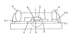
図1は、本発明の薄膜コンデンサの断面を示すものである。図2は図1中丸印部分の容量発生領域部分の拡大断面図であり、図3は保護膜を省略した状態の平面図である。
【0033】
図において1は支持基板であり、2は下部電極層であり、3は薄膜誘電体層であり、4は上部電極層であり、6は上部引出し電極であり、7は保護層であり、8、9は端子部である。また、薄膜誘電体層3および上部電極層4の周囲には、絶縁体層5が配置される。
【0034】
支持基板1はアルミナなどのセラミック基板、サファイアなどの単結晶基板などである。そして、支持基板1の表面には、下部電極層2が形成されている。下部電極層2、薄膜誘電体層3、上部電極層4は支持基板上の全面に同一バッチで形成され、全層のスパッタ終了後に、先ず薄膜誘電体層3および上部電極層4が所定形状のレジスト層を用いて同一形状に物理的にエッチングされ、その後に下部電極層2が所定形状のレジスト層を用いて物理的または化学的にエッチングされる。
【0035】
下部電極層2は、薄膜誘電体層3の形成に高温スパッタが必要となるため、高融点でしかも貴金属であるPtなどである。この下部電極層2は、例えば、基板温度150℃から600℃で形成されている。その後、薄膜誘電体層3のスパッタ温度である700〜900℃へ加熱され、スパッタ開始まで一定時間保持することにより平坦な薄膜となる。尚、図1中、符号21は、下部電極層2の一部を端子部9が形成される部位にまで延出される端子配置部である。
【0036】
この下部電極層2の厚みは、端子部9から容量発生領域までの抵抗成分、下部電極層2の連続性(いずれも厚みが厚い方が望ましい)及び支持基板1との密着性(厚みが相対的に薄い方が望ましい)を考慮して決定され、例えば、0.1〜10μmとなっている。例えば、0.1μmよりも小さくなると、電極自身の抵抗が大きくなると同時に、電極の連続性がなくなり、信頼性が劣るようになる。一方、10μm以上にすると支持基板1との密着信頼性が低下する。
【0037】
尚、下部電極層2を構成する金属材料は、高融点の貴金属Pt、Pd以外に、Au、Ag、Cuなどを適用した3層構造とすることも可能である。
【0038】
薄膜誘電体層3は、少なくともBa、Sr、Tiを含有するペロブスカイト型酸化物結晶粒子から成る高誘電率の誘電体層である。この薄膜誘電体層3は、上述の下部電極層2の表面に形成されている。例えば、ペロブスカイト型酸化物結晶粒子が得られる誘電体をターゲットとして、スパッタリングを行なう。例えば、基板温度を800℃として、厚みを考慮した時間だけ成膜を行う。高温でスパッタを行なうことにより、スパッタ後の熱処理を行なうこと無く、高誘電率で損失の低い薄膜誘電体層が得られる。
【0039】
上部電極層4の材料としては電極の抵抗を下げるため、抵抗率の小さなAuが望ましく、その他に、Ag、Cuなども使用できるが、薄膜誘電体層との密着性向上のためにはPt、Pdなどの高融点貴金属が望ましい。この上部電極層4の厚みは0.1〜10μmとなっている。厚みの下限については下部電極層2と同様に、電極自身の抵抗を考慮して設定される。また、厚みの上限については密着性の低下を考慮して設定される。尚、図1中において、符号61、62は、上部電極層4の一部が延出または同一工程で形成されるものであり、端子部8、9が形成される部位にまで延出される端子配置部である。
本発明の薄膜コンデンサにおいては、上述の様に、下部電極層2、薄膜誘電体層3、上部電極層4を同一バッチでスパッタ成膜でき、大気に曝すこと無く上部電極層まで成膜できるので、下部電極層−薄膜誘電体層間、薄膜誘電体層−上部電極層間に油脂等の、余分な付着が起こらないので、密着性が大幅に改善され、下部電極層−薄膜誘電体層間、薄膜誘電体層−上部電極層間への水分等の浸入を防止することができ、耐湿性を大幅に改善することができる。
【0040】
絶縁層5は、下部電極層2の突起部、薄膜誘電体層3、上部電極層4の周囲に形成されるものであり、材料は、SiO2、Si3N4等のセラミックスなどである。
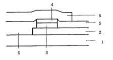
このような絶縁層5は、例えば、下部電極層2、上部電極層4及び支持基板1上に形成され、上部電極層4の上面のみが露出するように、ドライエッチングで不要部分を除去する。成膜、エッチングの様子を図4に示す。絶縁層5をスパッタで成膜する場合、スパッタでは、ターゲットのある一点から色々な方向にターゲット構成物質が放出されるので、基板上のある一点には色々な方向から飛来したターゲット構成物質が堆積していくことになる。ところが、ドライエッチングでは並行に置かれたエッチング装置の電極間で加速されたイオンにより、エッチングが行なわれるため、膜に垂直方向にエッチングが進行する。本発明においては上部電極層の最上面には絶縁層との密着性が悪いAuを用いており、エッチング中に上部電極層上の絶縁層とその周囲の絶縁層が完全に分断された時点で上部電極層上の絶縁層が自動的に除去できる。何らかの原因で除去できない場合は超音波洗浄または300℃程度の加熱で完全に除去することができる。この様な方法ではレジスト層のサイズ、位置合わせの精度は重要ではなく、上部電極よりも大きな窓を持つレジスト層を用いればよい。また、全くレジストを用いなくても同様の加工が可能である。エッチング時に上部電極層、および薄膜誘電体層の周囲の絶縁層もエッチングされ、浮遊容量発生の原因になるので初期の絶縁層の厚みは厚い方が望ましい。
【0041】
尚、絶縁層5は、少なくとも端子部8、9が形成される端子配置部を露出するように形成されている。
【0042】
上部引出し電極層6は上部電極層と端子配置部を連結させるために形成される。上部引出し電極には、Ag、Cu、などの安価で低抵抗な金属を用いることができる。サイズは浮遊容量と抵抗を考慮して決定する。
【0043】
また、保護膜7は、端子配置部61、62を露出するように形成されている。保護膜としては、SiO2,SiN,BCB(ベンゾシクロブテン)、ポリイミドなどが好適である。また、これらの材料の多層構造にしても良い。この保護膜6は、外部からの機械的な衝撃からの保護の他、湿度による劣化、薬品の汚染、酸化等を防止する役割を持っている。
【0044】
また、端子部8、9は、半田ボールや金属バンプなどが例示できる。また、金属ワイヤーのファーストボンディングを行い、所定長さで切断することにより、金などのバンプを形成しても構わない。
【0045】
以上のように、上述の薄膜コンデンサにおいて、容量発生領域は、下部電極層2と上部電極層4とに挟持された薄膜誘電体層3部分であり、同一レジスト層を用いて上部電極層と、薄膜誘電体層をエッチングすることで形成される。この時点では、支持基板1上には、下部電極層2、薄膜誘電体層3、上部電極層4が全面に形成されているだけであり、制約事項がない状態で精度よく下部電極層2の突起部、薄膜誘電体層3、上部電極層4を形成することができる。従って、容量発生領域の平面積を小さくすることも容易となり、高周波回路に用いるコンデンサを簡単に達成できることになる。
【0046】
しかも、薄膜誘電体層3を平坦な下部電極層2の段差の全くない面に被着形成できるため、薄膜誘電体層3中に段切れが発生したり、また、上部電極層4中に段切れが発生することが皆無となる。
【0047】
尚、絶縁層5が存在するために、下部電極層2と上部電極層4との間で、不要な容量成分が発生する可能性があるものの、容量発生領域の下部電極層2と上部電極層4との間隔に比較して、容量発生領域の周囲の下部電極層2と上部引出し電極6との間隔が非常に広いため、ここで発生する容量は、容量発生領域の容量に比較して無視できる。仮に、容量発生領域の周囲に発生する不要な容量をさらに小さくするためには、絶縁層を厚くすればよいが、その為には上部電極層も厚くする必要がある。
【0048】
特に、薄膜誘電体層3に(BaxSr1-x)TiO3などのように、下部電極層2と上部電極層4との間に直流バアイスを印加して、薄膜誘電体層3の誘電率を変化させ、もって、容量特性を調整できるチューナブル薄膜コンデンサにおいては、上部電極層4、下部電極層2での抵抗成分を小さくすることができるため、(薄膜誘電体層3中に段切れが発生することが皆無とすることができるため)薄膜誘電体層3にかかる電圧のバラツキを防止でき、安定したチューナビリティーが得られるものとなる。
【0049】
【実施例】
支持基板1としてサファイアR基板上に、下部電極層2としてPtを、基板温度500℃でスパッタ法により形成した。薄膜誘電体層3として(Ba0.5Sr0.5)TiO3からなるターゲットを用いて同一バッチで成膜した。これは、基板温度は800℃、成膜時間は15分で成膜を行なった。成膜開始前にPt電極の平坦化のためのアニールとして800℃で15分間保持した。その上に上部電極層4としてPtおよびAu電極層を同一バッチで形成し、取り出し後10μmφのレジスト層を形成し、ECR装置により上部電極層と薄膜誘電体層をエッチングし、再度下部電極用のレジスト層を形成し、ECRでエッチングし薄膜コンデンサを形成した。レジスト層剥離後、SiO2層をスパッタで600℃で成膜し、レジスト層を剥離後、ECRで15分程度エッチングし、上部電極層上のSiO2層のみを除去した。部分的に除去されていない上部電極層上のSiO2層については純水中で超音波洗浄することにより完全に除去した。最後に上部取り出し電極としてAuをスパッタ成膜し、不要部をエッチングで除去した。
インピーダンスアナライザによる測定の結果、容量は約1pFであり、ピコアンペアメーターによる測定の結果、リーク電流は10-12Aのオーダーであり、容量が小さく、リーク特性の良い薄膜キャパシタが得られた。
【0050】
即ち、各電極層、薄膜誘電体層で段切れがなく、また、電極部分の損失が低下し、高周波領域でも安定した容量素子として用いることができることを確認した。
【0051】
【発明の効果】
本発明の薄膜コンデンサの製造方法は、下部電極層、薄膜誘電体層、上部電極層を同一バッチで支持基板全面に形成した後、上部電極層上に所定形状のレジスト層を形成し、同一レジスト層を用いて、上部電極層、薄膜誘電体層の一部を順次アルゴンエッチング等により、エッチングを行なうことで薄膜誘電体層、上部電極層を平面積および形状の等しいものに形成する薄膜コンデンサの製造方法であって、下部電極層を150℃以上前記薄膜誘電体層の成膜温度より低温で成膜した後に、前記薄膜誘電体層の成膜温度に加熱して、前記薄膜誘電体層の成膜開始まで一定時間保持してアニールすることで平坦な下部電極層を得ることを特徴とするものである。そして、薄膜誘電体層を取り囲むように絶縁層が形成されている。
【0052】
これにより、薄膜誘電体層及び上部電極層で段切れがなく、また、容量発生領域の上部電極層、下部電極層の厚みを極力厚くすることが可能となり、電極損失を有効に抑えることができる薄膜コンデンサとなる。
【0053】
特に、上部電極層の平面積によってコンデンサの容量がほぼ決定されるため、フォトリソグラフィの工程において位置合わせの精度を全く必要とせず、安定した容量特性を確実に得ることができる。
【0054】
特に、下部電極層、上部電極に直流バイアスを印加して、薄膜誘電体層の誘電率を変化させるチューナブル薄膜コンデンサにおいては、電極内で電位バラツキを抑えることができる。
【図面の簡単な説明】
【図1】本発明の薄膜コンデンサの製造方法で作製した薄膜コンデンサの断面図である。
【図2】本発明の薄膜コンデンサの製造方法で作製した薄膜コンデンサの主要部分の断面図である。
【図3】本発明の薄膜コンデンサの製造方法で作製した、保護膜、端子部を省略した状態の薄膜コンデンサの平面図である。
【図4】本発明の絶縁層の成膜、エッチング工程の説明図である。[0001]
BACKGROUND OF THE INVENTION
The present invention relates to a thin film capacitor in which a dielectric layer is formed by a thin film technique, and more particularly to a method for manufacturing a low-capacity thin film capacitor having a high self-resonance frequency and low loss even at a high frequency.
[0002]
[Prior art]
One type of capacitor is a thin film capacitor in which an electrode layer and a dielectric layer, which are constituent elements of the capacitor, are formed of a thin film. In general, a thin film-like lower electrode layer, a dielectric layer, and an upper electrode layer are laminated in this order on an electrically insulating support substrate. In such a thin film capacitor, the lower electrode layer and the upper electrode layer are formed by sputtering, vacuum deposition, or the like, respectively, and the dielectric layer is also formed by sputtering, sol-gel method, or the like. In manufacturing such a thin film capacitor, a photolithography technique is usually used as follows. First, after forming a conductor layer to be a lower electrode layer on the entire surface of the insulating support substrate, only necessary portions are covered with a resist, and then unnecessary portions are removed by wet etching or dry etching to form a lower portion of a predetermined shape. An electrode layer is formed. Next, a dielectric layer to be a thin film dielectric layer is formed on the entire surface of the support substrate, and unnecessary portions are removed to form a thin film dielectric layer having a predetermined shape in the same manner as the lower electrode layer. Finally, a conductor layer to be an upper electrode layer is formed on the entire surface, and unnecessary portions are removed to form an upper electrode layer having a predetermined shape. Also, surface mounting is possible by forming a protective layer and solder bumps. In addition, as a material of the thin film dielectric layer, a dielectric material made of (Ba x Sr 1-x ) y Ti 1-y O 3 is used, and a predetermined potential is applied between the upper electrode layer and the lower electrode layer. A tunable thin film capacitor that controls the capacitance by changing the dielectric constant of the dielectric layer has the same structure.
[0003]
In order to use a thin film capacitor as a capacitor in a high frequency circuit, for example, the self-resonant frequency needs to be located on the high frequency side from the frequency used. Such a thin film capacitor can be obtained by reducing the inductance in the lower electrode layer and the upper electrode layer. A thin film capacitor having a small inductance is disclosed in, for example, Japanese Patent Application Laid-Open No. 8-241830.
[0004]
[Problems to be solved by the invention]
As described above, in order to use a thin film capacitor as a capacitor in a high frequency circuit, the self-resonant frequency needs to be located on the high frequency side with respect to the frequency used, and it is necessary that the inductance is small. The loss of the layer and the upper electrode layer must also be low. This is because even if the resonance point is on the higher frequency side than the frequency at which the capacitor is used, the impedance due to the capacitor is small at the frequency near the resonance point, so that the resistance component is dominant in the capacitor having a large loss. Therefore, in order to reduce the loss due to the lower electrode layer and the upper electrode layer, it is necessary to use a metal having a low resistivity and to make the lower electrode layer and the upper electrode layer as thick as possible.
[0005]
In addition, by reducing the capacitance of the capacitor, the self-resonant frequency can be shifted to the higher frequency side, and the increase in loss due to the influence of resonance can be reduced. To reduce the capacitance of the capacitor, it is necessary to reduce the plane area of the capacitance generation region composed of the lower electrode layer and the thin film dielectric layer sandwiched between the upper electrode layer, but to reduce the capacitor plane area. As a result, a step that degrades the leakage characteristics is generated in the dielectric portion constituting the capacitor, and the reliability is lowered. In addition, the accuracy of alignment in the manufacturing process becomes strict, resulting in a decrease in yield.
[0006]
Further, increasing the thickness of the electrode layer in order to reduce the loss due to the electrode layer described above further increases the level difference.
[0007]
Also, in conventional thin film capacitors, even when a low melting point metal is used as an electrode or a high melting point metal is used, the microstructure is not taken into account, resulting in poor adhesion, resulting in reliability. It is supposed to be inferior in moisture resistance.
[0008]
The present invention has been devised in view of the above-mentioned problems, and its purpose is that the electrode loss of the lower electrode layer and the upper electrode is small, and the plane area of the capacitance generation region needs to be aligned accurately. An object of the present invention is to provide a thin film capacitor that can be formed with high accuracy without any problems, simplifies the process.
[0009]
It is another object of the present invention to provide a thin film capacitor that eliminates a step, improves reliability, improves adhesion between a substrate, an electrode, and a dielectric, and has improved moisture resistance.
[0010]
[Means for Solving the Problems]
In the method of manufacturing a thin film capacitor of the present invention, a lower electrode layer, a thin film dielectric layer, and an upper electrode layer are formed in the same batch on the entire surface of the support substrate, and then a resist layer having a predetermined shape is formed on the upper electrode layer. Using the resist layer, the upper electrode layer and a part of the thin film dielectric layer are sequentially etched by argon etching or the like so that the thin film dielectric layer and the upper electrode layer have the same plane area and shape. In the method of manufacturing a thin film capacitor to be formed, after the lower electrode layer is formed at a temperature lower than the film formation temperature of the thin film dielectric layer by 150 ° C. or more , the film is heated to the film formation temperature of the thin film dielectric layer, A flat lower electrode layer is obtained by annealing for a certain period of time until the thin film dielectric layer starts to be formed .
[0011]
Further, the lower electrode layer has a protrusion having the same shape and area as the upper electrode layer and the thin film dielectric layer immediately below the thin film dielectric layer.
[0012]
An insulating layer is disposed around the protrusion of the lower electrode layer, the thin film dielectric layer, and the upper electrode layer.
The thin film dielectric layer is made of a perovskite oxide crystal containing at least Ba, Sr, and Ti .
The thin film dielectric layer has a dielectric layer made of at least one of SiOx or SiNx interposed at the interface between the lower electrode and the upper electrode layer.
Further, the insulator layer is made of SiOx or SiNx.
Further, flat Pt or Pd is used as the lower electrode layer.
The lower electrode layer is made of any of Au, Ag, and Cu, and one layer of either Pt or Pd is interposed at the interface between the support substrate and the dielectric layer.
The lower electrode layer is made of either Pt or Pd and an Au alloy.
The upper electrode layer has a two-layer structure composed of either Pt or Pd and Au from the thin film dielectric layer side.
The upper electrode layer has a three-layer structure of either a Pt or Pd metal layer, a Cu or Ag metal layer, and a metal layer made of Au from the thin film dielectric side.
[0014]
In addition, after forming a metal layer comprising at least Pt or Pd out of the metal layer constituting the lower electrode layer or the upper electrode layer at a temperature lower than the film formation temperature of the thin film dielectric layer, the thin film dielectric thin layer is formed. A thin film capacitor manufacturing method characterized in that a flat electrode is obtained by heating to a temperature.
[0015]
In addition, after preparing the lower electrode layer, thin film dielectric layer, and upper electrode layer having a predetermined shape, an insulating layer is formed on the entire surface of the support substrate by sputtering or the like, and etched using a resist film having a window larger than the upper electrode. A method for manufacturing a thin film capacitor, characterized in that an insulating layer having a predetermined shape is obtained.
[0016]
The lower electrode layer of a predetermined shape, the thin-film dielectric layer was fabricated upper electrode layer, the entire surface of the substrate to the insulating layer is deposited by sputtering or the like, by performing the error etching to the upper electrode layer is exposed, the resist layer A thin film capacitor manufacturing method characterized by obtaining an insulating layer having a predetermined shape without using it. In addition, after the lower electrode layer, the thin film dielectric layer, and the upper electrode layer are formed, an insulating layer is formed on the entire surface of the support substrate by sputtering or the like, and etching is performed between the insulating layer on the upper electrode layer and the surrounding insulating layer. The method of manufacturing a thin film capacitor is characterized in that the insulating layer on the upper electrode layer is removed at the time when is divided.
[0017]
Thereby, the thickness of the upper electrode and the lower electrode can be increased, and the loss due to the electrodes can be reduced. Further, since the thin film dielectric layer exists only directly below the upper electrode layer, and the shape and the planar area of the thin film dielectric layer and the upper electrode layer are equal, the capacitance of the capacitor element can be accurately controlled.
[0018]
In addition, since the lower electrode layer has a protrusion having a shape and a planar area equal to those of the upper electrode layer and the thin film dielectric layer immediately below the thin film dielectric layer, the capacitance of the capacitor element can be controlled more accurately.
[0019]
Furthermore, in the above structure, after forming the lower electrode layer, the thin film dielectric layer, and the upper electrode layer on the entire surface of the support substrate, a resist layer having a predetermined shape is formed on the upper electrode layer, and the same resist layer is used. Then, the upper electrode layer and the thin film dielectric layer are physically etched sequentially by argon etching or the like to form the protrusions of the lower electrode layer, the thin film dielectric layer, and the upper electrode layer having the same flat area and shape. The lower electrode layer, the dielectric layer, and the upper electrode layer can be formed by sputtering in one batch. After forming the lower electrode, it is not necessary to expose to the atmosphere after forming the dielectric, so that adhesion of moisture, fats and oils will not occur on the film surface, and adhesion between the electrode and dielectric can be greatly improved, Since adhesion can be improved, moisture resistance is improved, and reliability as a capacitor element is also improved. Moreover, since the same resist can be used for one batch of sputtering and etching of the upper electrode layer and the thin film dielectric layer, the thin film capacitor manufacturing process is greatly simplified.
[0020]
In addition, since the insulator layer is disposed around the protrusion of the lower electrode layer, the thin film dielectric layer, and the upper electrode layer, the dielectric layer is directly surrounded by the insulator layer. As a result, the dielectric side surface is sealed with an insulating layer having good adhesion to the dielectric, so that the moisture resistance of the dielectric side surface is improved and the reliability as a capacitor element is improved.
[0021]
Such an insulating layer is a resist film having a lower electrode layer, a thin film dielectric layer, and an upper electrode layer having a predetermined shape, and then an insulating layer is formed on the entire surface of the substrate by sputtering or the like, and has a window larger than the upper electrode. It can be manufactured by performing etching using.
[0022]
Furthermore, after forming a lower electrode layer, a thin film dielectric layer, and an upper electrode layer having a predetermined shape, an insulating layer is formed on the entire surface of the substrate by sputtering or the like, and physically etched without using a resist layer. Fabrication is also possible by obtaining an insulating layer having a predetermined shape.
[0023]
Further, since the thin film dielectric layer is a thin film capacitor characterized by comprising a perovskite oxide crystal containing at least Ba, Sr, and Ti, the loss of the dielectric itself can be reduced. A tunable thin film capacitor whose dielectric constant can be changed by applying an external voltage can also be used. In particular, a DC bias is applied to the lower electrode layer and the upper electrode layer, but by increasing the thickness of the electrode in the capacity generation region, there is no bias bias and stable dielectric constant control is possible.
[0024]
When D1 is SiO x or SiN x and D2 is (Ba x Sr 1-x ) y Ti 1-y O 3 , three layers of D1 / D2 / D1 are formed as the thin film dielectric layer from the lower electrode side. By using the structure, the upper and lower sides of (Ba x Sr 1-x ) y Ti 1-y O 3 are sandwiched by an insulating layer such as SiO x or SiN x that has better adhesion than the metal layer. The moisture resistance is improved and the reliability as a capacitor element can be improved.
[0025]
Further, since the insulator layer is made of SiO x or SiN x , the moisture resistance of the thin film dielectric layer is improved, and furthermore, these low dielectric constant insulator layers are located on the side surfaces of the thin film dielectric layer. Therefore, the generation of stray capacitance can be reduced.
[0026]
Further, by using flat Pt or Pd as the lower electrode layer, the adhesion with the thin film dielectric layer is improved, and the unevenness of the thin film dielectric layer is reduced, so that the breakdown voltage is high and the leakage current is reduced. , Leading to improved reliability. In addition, since these metals have a high melting point, a thin film dielectric layer can be formed immediately after film formation at a high temperature, forming a thin film dielectric layer that is dense, has few oxygen defects, and has low loss. can do. Further, in the production of a tunable thin film capacitor, a thin film dielectric having a large change rate of dielectric constant can be formed.
[0027]
In addition, when Me1 is Pt or Pd and Me2 is either Au, Ag, or Cu, a three-layer structure of Me1 / Me2 / Me1 from the support substrate side is used as the lower electrode layer, and at least the thin film dielectric side The flat Me1 layer enables the formation of a thin film dielectric layer that is dense, has few oxygen defects, and has a small loss. In addition to being able to form a dielectric, it is possible to produce an electrode layer that has good adhesion to the support substrate and the thin film dielectric layer, is inexpensive, and has a low resistivity.
Also, when Me is Pt or Pd, by using a flat Me-Au alloy as the lower electrode layer, it is more stable and has good adhesion to the support substrate and the thin film dielectric layer. An electrode layer with a low rate can be manufactured.
[0028]
In addition, when Me is Pt or Pd, the upper electrode layer uses a two-layer structure of Me / Au from the thin film dielectric layer side, so that it has good adhesion to the thin film dielectric layer, and the insulator layer and Can produce an upper electrode layer with poor adhesion. When the insulating layer is manufactured by the above-described method, the insulating layer on the upper electrode having poor adhesion can be completely removed. Further, since the upper electrode layer having a low resistivity can be manufactured, the loss as a thin film capacitor can be reduced.
[0029]
In addition, when Me1 is Pt or Pd, Me2 is Cu, and Ag, the upper electrode layer is made of a three-layer structure of Me1 / Me2 / Au from the dielectric side as the upper electrode layer. I can do it.
[0030]
After forming at least the Pt and Pd layers of the metal layer constituting the electrode layer at a temperature lower than the film formation temperature of the thin film dielectric layer, the film is heated to the film formation temperature of the thin film dielectric layer to form the thin film dielectric layer Although a flat electrode can be obtained by holding for a certain period of time until the start of film formation , this method eliminates the need to remove the sample from the chamber and perform annealing after forming the metal layer once. Film formation and annealing can be performed in the same batch.
[0031]
DETAILED DESCRIPTION OF THE INVENTION
Hereinafter, the thin film capacitor of the present invention will be described in detail with reference to the drawings.
[0032]
FIG. 1 shows a cross section of a thin film capacitor of the present invention. FIG. 2 is an enlarged cross-sectional view of the capacitance generation region portion of the circled portion in FIG. 1, and FIG. 3 is a plan view of the state where the protective film is omitted.
[0033]
In the figure, 1 is a support substrate, 2 is a lower electrode layer, 3 is a thin film dielectric layer, 4 is an upper electrode layer, 6 is an upper lead electrode, 7 is a protective layer, 8 , 9 are terminal portions. An
[0034]
The
[0035]
The
[0036]
The thickness of the
[0037]
The metal material constituting the
[0038]
The thin
[0039]
As the material of the
In the thin film capacitor of the present invention, as described above, the
[0040]
The insulating
Such an insulating
[0041]
The insulating
[0042]
The upper
[0043]
Further, the
[0044]
The
[0045]
As described above, in the above-described thin film capacitor, the capacitance generation region is the thin
[0046]
Moreover, since the thin
[0047]
Although the insulating
[0048]
In particular, the direct current baice is applied between the
[0049]
【Example】
Pt as the
As a result of measurement with an impedance analyzer, the capacitance was about 1 pF, and as a result of measurement with a picoampere meter, a leakage current was on the order of 10 −12 A, and a thin film capacitor with small capacitance and good leakage characteristics was obtained.
[0050]
That is, it was confirmed that each electrode layer and the thin film dielectric layer had no step breakage, the loss of the electrode portion was reduced, and it could be used as a stable capacitive element even in a high frequency region.
[0051]
【The invention's effect】
In the method of manufacturing a thin film capacitor according to the present invention, a lower electrode layer, a thin film dielectric layer, and an upper electrode layer are formed in the same batch on the entire surface of a support substrate, and then a resist layer having a predetermined shape is formed on the upper electrode layer. A thin film capacitor in which a part of the upper electrode layer and the thin film dielectric layer are sequentially etched by argon etching or the like to form the thin film dielectric layer and the upper electrode layer in the same plane area and shape. In the manufacturing method, the lower electrode layer is formed at 150 ° C. or more at a temperature lower than the film formation temperature of the thin film dielectric layer, and then heated to the film formation temperature of the thin film dielectric layer, A flat lower electrode layer is obtained by annealing while holding for a certain period of time until the start of film formation. An insulating layer is formed so as to surround the thin film dielectric layer.
[0052]
As a result, the thin-film dielectric layer and the upper electrode layer are not stepped, and the thickness of the upper electrode layer and the lower electrode layer in the capacity generation region can be increased as much as possible, thereby effectively suppressing electrode loss. It becomes a thin film capacitor.
[0053]
In particular, since the capacitance of the capacitor is substantially determined by the plane area of the upper electrode layer, the alignment accuracy is not required at all in the photolithography process, and stable capacitance characteristics can be obtained with certainty.
[0054]
In particular, in a tunable thin film capacitor that changes the dielectric constant of the thin film dielectric layer by applying a direct current bias to the lower electrode layer and the upper electrode, potential variation can be suppressed within the electrode.
[Brief description of the drawings]
FIG. 1 is a cross-sectional view of a thin film capacitor produced by the method for producing a thin film capacitor of the present invention.
FIG. 2 is a cross-sectional view of a main part of a thin film capacitor manufactured by the method for manufacturing a thin film capacitor of the present invention.
FIG. 3 is a plan view of a thin film capacitor in a state where a protective film and a terminal portion are omitted , manufactured by the method for manufacturing a thin film capacitor of the present invention.
FIG. 4 is an explanatory diagram of an insulating layer deposition and etching process according to the present invention.
Claims (6)
前記下部電極層を150℃以上前記薄膜誘電体層の成膜温度より低温で成膜した後に、前記薄膜誘電体層の成膜温度に加熱して、前記薄膜誘電体層の成膜開始まで一定時間保持してアニールすることで平坦な下部電極層を得ることを特徴とする薄膜コンデンサの製造方法。After the lower electrode layer, the thin film dielectric layer, and the upper electrode layer are formed in the same batch on the entire surface of the support substrate, a resist layer having a predetermined shape is formed on the upper electrode layer, and the upper electrode layer is formed using the same resist layer. A method of manufacturing a thin film capacitor in which a part of the thin film dielectric layer is sequentially etched to form the thin film dielectric layer and the upper electrode layer in the same plane area and shape,
After the lower electrode layer is formed at a temperature of 150 ° C. or more and lower than the film formation temperature of the thin film dielectric layer, the film is heated to the film formation temperature of the thin film dielectric layer and constant until the film formation start of the thin film dielectric layer A method for producing a thin film capacitor, characterized in that a flat lower electrode layer is obtained by annealing for a period of time.
前記下部電極層、前記薄膜誘電体層、前記上部電極層を作製した後、前記支持基板全面に絶縁層を成膜し、エッチングを、前記上部電極層上の前記絶縁層とその周囲の前記絶縁層とが分断された時点で止め、前記上部電極層上の前記絶縁層を除去することを特徴とする請求項1ないし5のいずれかに記載の薄膜コンデンサの製造方法。 After forming the lower electrode layer, the thin film dielectric layer, and the upper electrode layer, an insulating layer is formed on the entire surface of the support substrate, and etching is performed to form the insulating layer on the upper electrode layer and the insulating layer around the insulating layer. 6. The method for manufacturing a thin film capacitor according to claim 1, wherein the insulating layer on the upper electrode layer is removed when the layer is separated from the upper electrode layer.
Priority Applications (1)
| Application Number | Priority Date | Filing Date | Title |
|---|---|---|---|
| JP2001395376A JP3996765B2 (en) | 2001-12-26 | 2001-12-26 | Thin film capacitor manufacturing method |
Applications Claiming Priority (1)
| Application Number | Priority Date | Filing Date | Title |
|---|---|---|---|
| JP2001395376A JP3996765B2 (en) | 2001-12-26 | 2001-12-26 | Thin film capacitor manufacturing method |
Related Child Applications (1)
| Application Number | Title | Priority Date | Filing Date |
|---|---|---|---|
| JP2007008452A Division JP4183200B2 (en) | 2007-01-17 | 2007-01-17 | Thin film capacitor manufacturing method |
Publications (2)
| Publication Number | Publication Date |
|---|---|
| JP2003197464A JP2003197464A (en) | 2003-07-11 |
| JP3996765B2 true JP3996765B2 (en) | 2007-10-24 |
Family
ID=27601807
Family Applications (1)
| Application Number | Title | Priority Date | Filing Date |
|---|---|---|---|
| JP2001395376A Expired - Fee Related JP3996765B2 (en) | 2001-12-26 | 2001-12-26 | Thin film capacitor manufacturing method |
Country Status (1)
| Country | Link |
|---|---|
| JP (1) | JP3996765B2 (en) |
-
2001
- 2001-12-26 JP JP2001395376A patent/JP3996765B2/en not_active Expired - Fee Related
Also Published As
| Publication number | Publication date |
|---|---|
| JP2003197464A (en) | 2003-07-11 |
Similar Documents
| Publication | Publication Date | Title |
|---|---|---|
| US6806553B2 (en) | Tunable thin film capacitor | |
| JP2006196871A (en) | Thin-film capacitor, variable capacitor, and electronic component | |
| JPWO2011010638A1 (en) | Dielectric thin film element and manufacturing method thereof | |
| JPH0878283A (en) | Thin film capacitor | |
| JP2008252011A (en) | Dielectric capacitor | |
| JP2009010114A (en) | Dielectric thin-film capacitor | |
| CN107045913B (en) | Electronic component | |
| EP0107515A2 (en) | Methods of making Josephson junction devices | |
| JP3996765B2 (en) | Thin film capacitor manufacturing method | |
| US9941858B2 (en) | Electricoacoustic component with structured conductor and dielectric layer | |
| JPS59144162A (en) | Manufacture of thin film circuit | |
| JP4183200B2 (en) | Thin film capacitor manufacturing method | |
| JP3898638B2 (en) | Capacitance variable thin film capacitors and high frequency components | |
| JP2007201158A (en) | Capacitor | |
| JP3898637B2 (en) | Capacitance variable capacitor circuit, variable capacitance thin film capacitor element and high frequency component | |
| JP2003045742A (en) | Thin film capacitor | |
| WO2008026708A1 (en) | Capacitor and high frequency component | |
| JP2005136074A (en) | Capacitor, serial capacitor and variable capacitor | |
| JP4535817B2 (en) | Thin film capacitors, thin film capacitor arrays and electronic components | |
| JP3898648B2 (en) | Capacitance variable thin film capacitors and high frequency components | |
| JPH10135077A (en) | Thin film capacitor | |
| JP2003045743A (en) | Thin film capacitor | |
| JPH05326313A (en) | Capacitor and manufacture thereof | |
| JP4493405B2 (en) | Variable capacitor, circuit module and communication device | |
| JP2003109842A (en) | Thin film capacitor |
Legal Events
| Date | Code | Title | Description |
|---|---|---|---|
| A621 | Written request for application examination |
Free format text: JAPANESE INTERMEDIATE CODE: A621 Effective date: 20040607 |
|
| A977 | Report on retrieval |
Free format text: JAPANESE INTERMEDIATE CODE: A971007 Effective date: 20061110 |
|
| A131 | Notification of reasons for refusal |
Free format text: JAPANESE INTERMEDIATE CODE: A131 Effective date: 20061121 |
|
| A521 | Written amendment |
Free format text: JAPANESE INTERMEDIATE CODE: A523 Effective date: 20070117 |
|
| A131 | Notification of reasons for refusal |
Free format text: JAPANESE INTERMEDIATE CODE: A131 Effective date: 20070309 |
|
| A521 | Written amendment |
Free format text: JAPANESE INTERMEDIATE CODE: A523 Effective date: 20070508 |
|
| TRDD | Decision of grant or rejection written | ||
| A01 | Written decision to grant a patent or to grant a registration (utility model) |
Free format text: JAPANESE INTERMEDIATE CODE: A01 Effective date: 20070710 |
|
| A61 | First payment of annual fees (during grant procedure) |
Free format text: JAPANESE INTERMEDIATE CODE: A61 Effective date: 20070803 |
|
| FPAY | Renewal fee payment (event date is renewal date of database) |
Free format text: PAYMENT UNTIL: 20100810 Year of fee payment: 3 |
|
| R150 | Certificate of patent or registration of utility model |
Ref document number: 3996765 Country of ref document: JP Free format text: JAPANESE INTERMEDIATE CODE: R150 Free format text: JAPANESE INTERMEDIATE CODE: R150 |
|
| FPAY | Renewal fee payment (event date is renewal date of database) |
Free format text: PAYMENT UNTIL: 20100810 Year of fee payment: 3 |
|
| FPAY | Renewal fee payment (event date is renewal date of database) |
Free format text: PAYMENT UNTIL: 20110810 Year of fee payment: 4 |
|
| FPAY | Renewal fee payment (event date is renewal date of database) |
Free format text: PAYMENT UNTIL: 20110810 Year of fee payment: 4 |
|
| FPAY | Renewal fee payment (event date is renewal date of database) |
Free format text: PAYMENT UNTIL: 20120810 Year of fee payment: 5 |
|
| FPAY | Renewal fee payment (event date is renewal date of database) |
Free format text: PAYMENT UNTIL: 20130810 Year of fee payment: 6 |
|
| LAPS | Cancellation because of no payment of annual fees |