JP3972045B2 - Multilayer Lange coupler - Google Patents
Multilayer Lange coupler Download PDFInfo
- Publication number
- JP3972045B2 JP3972045B2 JP2005083728A JP2005083728A JP3972045B2 JP 3972045 B2 JP3972045 B2 JP 3972045B2 JP 2005083728 A JP2005083728 A JP 2005083728A JP 2005083728 A JP2005083728 A JP 2005083728A JP 3972045 B2 JP3972045 B2 JP 3972045B2
- Authority
- JP
- Japan
- Prior art keywords
- lines
- multilayer
- lange coupler
- coupled
- coupled lines
- Prior art date
- Legal status (The legal status is an assumption and is not a legal conclusion. Google has not performed a legal analysis and makes no representation as to the accuracy of the status listed.)
- Expired - Fee Related
Links
Images


Description
本発明はランゲカプラに関し、特に、複数の結合線路を2つの配線層に形成した積層型のランゲカプラに関する。 The present invention relates to a Lange coupler, and more particularly to a stacked Lange coupler in which a plurality of coupled lines are formed in two wiring layers.
従来より、高周波伝送信号を分配するための素子としてカプラが広く用いられており、中でも、ランゲカプラは広帯域特性を有するカプラとして知られている。ランゲカプラには種々のタイプが存在するが、いずれのタイプも、複数の結合線路を平行に近接配置した構造を有している(特許文献1参照)。しかしながら、通常のランゲカプラは、基板上に各結合線路が平面的に配置されていることから、結合線路間の一部接続にボンディングワイヤを使用する必要があり、このため、製造工程が複雑化するなどの問題があった。 Conventionally, a coupler has been widely used as an element for distributing a high-frequency transmission signal. Among them, a Lange coupler is known as a coupler having a broadband characteristic. There are various types of Lange couplers, but each type has a structure in which a plurality of coupled lines are arranged close to each other in parallel (see Patent Document 1). However, in the normal Lange coupler, since each coupling line is arranged in a plane on the substrate, it is necessary to use a bonding wire for partial connection between the coupling lines, which complicates the manufacturing process. There were problems such as.
このような問題を解決したランゲカプラとして、いわゆる「積層型ランゲカプラ」が知られている。積層型ランゲカプラは、複数の結合線路を2つの配線層に形成することにより、結合線路間における結合を一部立体化した構造を有している。これにより、ボンディングワイヤによる接続が不要となり、製造工程をより簡素化することが可能となる。積層型ランゲカプラとしては、例えば、特許文献2に開示されたものが知られている。
しかしながら、特許文献1,2に記載されたランゲカプラは、いずれも結合線路が基板上に露出しているため、該ランゲカプラが搭載された高周波回路全体を例えばシールドケースなどグランド電位が与えられる導電部材で覆うと、この導電部材がカプラの特性に大きな影響を与え、実際の特性が設計値から大きくずれるという問題があった。一方、シールドケースなどで覆われていない場合には、実使用時に金属板などのグランド面を近づけるとインピーダンスが変化するなど、使用環境によって特性が変動するという問題が生じてしまう。さらに、結合線路が基板上に露出しているために、放射損失が大きいという問題もあった。 However, since the Lange couplers described in Patent Documents 1 and 2 both have the coupling line exposed on the substrate, the entire high-frequency circuit on which the Lange coupler is mounted is a conductive member to which a ground potential is applied, such as a shield case. When covered, there is a problem that this conductive member greatly affects the characteristics of the coupler, and the actual characteristics deviate greatly from the design values. On the other hand, when it is not covered with a shield case or the like, there arises a problem that the characteristics fluctuate depending on the use environment, for example, the impedance changes when a ground plane such as a metal plate is brought closer to the actual use. Furthermore, since the coupled line is exposed on the substrate, there is a problem that radiation loss is large.
しかも、特許文献2に記載された積層型ランゲカプラは、結合線路が立体的に形成されていることから、結合線路間を立体的に分離する絶縁層の厚さを十分に薄くしなければ、1層目の結合線路からグランド面までの距離と、2層目の結合線路からグランド面までの距離に大きな差が生じてしまい、結合線路間の対称性が損なわれるという問題もあった。 Moreover, in the multilayer Lange coupler described in Patent Document 2, since the coupled lines are three-dimensionally formed, if the thickness of the insulating layer that three-dimensionally separates the coupled lines is not sufficiently reduced, 1 There is also a problem that a large difference occurs between the distance from the coupling line in the layer to the ground plane and the distance from the coupling line in the second layer to the ground plane, and the symmetry between the coupling lines is impaired.
本発明は、このような問題点を解決すべくなされたものであって、設計値により近い特性を得ることができ、且つ、使用環境による特性の変動が小さい積層型ランゲカプラを提供することを目的とする。 The present invention has been made to solve such problems, and an object of the present invention is to provide a multilayer Lange coupler that can obtain characteristics closer to the design value and that has less fluctuation in characteristics depending on the use environment. And
また、本発明の他の目的は、結合線路間の対称性に優れた積層型ランゲカプラを提供することである。 Another object of the present invention is to provide a stacked Lange coupler having excellent symmetry between coupled lines.
本発明による積層型ランゲカプラは、第1の配線層に形成された互いに平行な第1及び第2の結合線路であって、一端が第1のポートに共通接続され、他端が第2のポートに共通接続された第1及び第2の結合線路と、前記第1の配線層とは異なる第2の配線層に形成された互いに平行な第3及び第4の結合線路であって、一端が第3のポートに共通接続され、他端が第4のポートに共通接続された第3及び第4の結合線路と、前記第1乃至第4の結合線路を挟み込むように形成された第1及び第2のグランドパターンとを備えることを特徴とする。 The multilayer Lange coupler according to the present invention is a first and second coupled line formed in a first wiring layer and parallel to each other, one end of which is commonly connected to the first port and the other end is a second port. First and second coupled lines connected in common to each other and third and fourth coupled lines formed in a second wiring layer different from the first wiring layer and parallel to each other, one end of which The third and fourth coupling lines that are commonly connected to the third port and the other end are commonly connected to the fourth port, and the first and fourth coupling lines sandwiched between the first to fourth coupling lines And a second ground pattern.
本発明によれば、グランドパターンによって結合線路が挟み込まれた構造を有していることから、積層型ランゲカプラが搭載された高周波回路全体をシールドケースによって覆った場合であっても、このシールドケースが特性に与える影響はほとんどなく、設計値に近い特性を得ることが可能となる。しかも、実使用時に金属板などのグランド面を近づけたり遠ざけたりしても、これによりインピーダンスが変化するようなことはほとんどなく、使用環境に応じた特性の変動を抑制することが可能となる。さらに、放射損失についても低減される。 According to the present invention, since the coupling line is sandwiched by the ground pattern, even if the entire high-frequency circuit on which the multilayer Lange coupler is mounted is covered by the shield case, the shield case There is almost no influence on the characteristics, and characteristics close to the design values can be obtained. In addition, even if the ground plane such as a metal plate is brought closer or away during actual use, the impedance hardly changes by this, and it is possible to suppress fluctuations in characteristics according to the use environment. Furthermore, radiation loss is also reduced.
第1乃至第4の結合線路の長さは、いずれも伝送信号の1/4波長に相当する長さに設定されていることが好ましい。これによれば、目的とする周波数にて良好な結合特性を得ることが可能となる。 The lengths of the first to fourth coupled lines are preferably set to a length corresponding to a quarter wavelength of the transmission signal. This makes it possible to obtain good coupling characteristics at the target frequency.
第1の配線層から第1のグランドパターンまでの距離と、第2の配線層から第2のグランドパターンまでの距離は、実質的に等しいことが好ましい。これによれば、結合線路間における高い対称性を得ることが可能となり、その結果、良好な結合特性を得ることが可能となる。 It is preferable that the distance from the first wiring layer to the first ground pattern and the distance from the second wiring layer to the second ground pattern are substantially equal. According to this, it is possible to obtain high symmetry between the coupled lines, and as a result, it is possible to obtain good coupling characteristics.
また、本発明による積層型ランゲカプラは、第1及び第2の結合線路の前記一端及び他端の近傍、並びに、第3及び第4の結合線路の前記一端及び他端の近傍に、インピーダンス調整パターンが形成されていることが好ましい。これによれば、結合線路の幅などを本来の設計値とは異なる幅に設定することが可能となり、その結果、設計の自由度が増大する。 Also, the multilayer Lange coupler according to the present invention has an impedance adjustment pattern in the vicinity of the one end and the other end of the first and second coupling lines and in the vicinity of the one end and the other end of the third and fourth coupling lines. Is preferably formed. According to this, it becomes possible to set the width | variety etc. of a coupling line to the width different from the original design value, As a result, the freedom degree of design increases.
インピーダンス調整パターンは、第1及び第2の結合線路の前記一端及び他端、並びに、第3及び第4の結合線路の前記一端及び他端からみて、伝送信号の1/4波長に相当する距離以内の位置に形成されていることが好ましい。インピーダンス調整パターンをこの範囲内に形成すれば、インピーダンス調整パターンによる高い調整効果を得ることが可能となる。 The impedance adjustment pattern is a distance corresponding to a quarter wavelength of the transmission signal when viewed from the one end and the other end of the first and second coupled lines and the one end and the other end of the third and fourth coupled lines. It is preferable that it is formed in the position within. If the impedance adjustment pattern is formed within this range, a high adjustment effect by the impedance adjustment pattern can be obtained.
インピーダンス調整パターンは、オープンスタブであることが好ましい。これによれば、高いインピーダンス調整効果を最も簡単に得ることが可能となる。 The impedance adjustment pattern is preferably an open stub. According to this, a high impedance adjustment effect can be obtained most easily.
オープンスタブの長さは、伝送信号の1/4波長に相当する長さ以内に設定することが好ましい。オープンスタブの長さを上記の長さに設定すれば、積層型ランゲカプラの平面形状を必要以上に大型化することなく、高い調整効果を得ることが可能となる。 The length of the open stub is preferably set within a length corresponding to a quarter wavelength of the transmission signal. If the length of the open stub is set to the above length, a high adjustment effect can be obtained without increasing the planar shape of the multilayer Lange coupler more than necessary.
このように、本発明によれば、グランドパターンによって結合線路が挟み込まれた構造を有していることから、積層型ランゲカプラが搭載された高周波回路全体をシールドケースによって覆った場合であっても、このシールドケースが特性に与える影響はほとんどなく、設計値に近い特性を得ることが可能となる。しかも、実使用時に金属板などのグランド面を近づけたり遠ざけたりしても、これによりインピーダンスが変化するようなことはほとんどなく、使用環境に応じた特性の変動を抑制することが可能となる。さらに、放射損失についても低減される。 Thus, according to the present invention, since the coupling line is sandwiched by the ground pattern, even when the entire high-frequency circuit on which the stacked Lange coupler is mounted is covered with a shield case, The shield case has little influence on the characteristics, and it is possible to obtain characteristics close to the design values. In addition, even if the ground plane such as a metal plate is brought closer or away during actual use, the impedance hardly changes by this, and it is possible to suppress fluctuations in characteristics according to the use environment. Furthermore, radiation loss is also reduced.
特に、インピーダンス調整パターンを設ければ、結合線路の幅などを本来の設計値とは異なる幅に設定することが可能となるため、作製精度の限界により、本来の設計値では結合線路を形成困難な積層型ランゲカプラであっても、これを容易に作製することが可能となる。 In particular, if an impedance adjustment pattern is provided, it is possible to set the width of the coupled line to a width different from the original design value. Therefore, it is difficult to form the coupled line with the original design value due to the limit of manufacturing accuracy. Even a multilayer type Lange coupler can be easily manufactured.
以下、添付図面を参照しながら、本発明の好ましい実施の形態について詳細に説明する。 Hereinafter, preferred embodiments of the present invention will be described in detail with reference to the accompanying drawings.
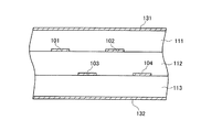
図1は、本発明の好ましい第1の実施形態にかかる積層型ランゲカプラ100の構造を示す透視平面図であり、図2は、図1に示すA−A線に沿った略断面図である。
FIG. 1 is a perspective plan view showing the structure of the multilayer Lange
図1及び図2に示すように、本実施形態による積層型ランゲカプラ100は、絶縁層111と絶縁層112との間に存在する配線層(第1の配線層)に形成された第1及び第2の結合線路101,102と、絶縁層112と絶縁層113との間に存在する配線層(第2の配線層)に形成された第3及び第4の結合線路103,104とを備えている。これら第1乃至第4の結合線路101〜104は、互いに平行に配置されており、このうち、第1及び第2の結合線路101,102の一端は第1のポート121に共通接続され、他端は第2のポート122に共通接続されている。また、第3及び第4の結合線路103,104の一端は第3のポート123に共通接続され、他端は第4のポート124に共通接続されている。
As shown in FIGS. 1 and 2, the multilayer
さらに、本実施形態による積層型ランゲカプラ100は、絶縁層111の表面に形成された第1のグランドパターン131と、絶縁層113の表面に形成された第2のグランドパターン132とを備えており、これによって、第1乃至第4の結合線路101〜104は、第1及び第2のグランドパターン131,132によって挟み込まれた構造を有している。
Furthermore, the multilayer Lange
図3は、本実施形態による積層型ランゲカプラ100の回路構成を模式的に示す図である。
FIG. 3 is a diagram schematically showing a circuit configuration of the multilayer Lange
図3に示すように、積層型ランゲカプラ100に含まれる第1乃至第4の結合線路101〜104は、第1の結合線路101、第3の結合線路103、第2の結合線路102、第4の結合線路104の順に平行配置されており、隣り合う結合線路が容量的に結合される。第1乃至第4の結合線路101〜104の長さLは互いに等しく、いずれも伝送信号の1/4波長に相当する長さに設定されている。例えば、伝送信号が24GHzである場合、絶縁層111〜113の比誘電率を6.3とすると、結合線路の長さLは約1.2mmとなる。また、第1乃至第4のポート121〜124は、1つが入力ポート、2つが出力ポートとして用いられ、残りの1つは例えば50Ωに終端される。
As shown in FIG. 3, the first to fourth coupled
第1乃至第4の結合線路101〜104の幅Wや、隣り合う結合線路間の間隔Sについても、伝送信号の周波数などに応じて設定されるが、隣り合う結合線路が異なる配線層に形成されていることから、結合線路間の間隔Sについては非常に自由度が高い。したがって、結合線路を形成する際の精度限界によって、平面的には形成不可能な狭い間隔であっても、これを実現することが可能となる。
The width W of the first to fourth coupled
上述のとおり、本実施形態による積層型ランゲカプラ100は、第1及び第2のグランドパターン131,132によって、第1乃至第4の結合線路101〜104が挟み込まれた構造を有している。つまり、各結合線路101〜104は、マイクロストリップ線路ではなく、ストリップ線路として機能する。このため、本実施形態による積層型ランゲカプラ100が搭載された高周波回路全体をシールドケースによって覆った場合であっても、このシールドケースが特性に与える影響はほとんどなく、設計値に近い特性を得ることが可能となる。しかも、実使用時に金属板などのグランド面を近づけたり遠ざけたりしても、これによりインピーダンスが変化するようなことはほとんどなく、使用環境に応じた特性の変動を抑制することが可能となる。さらに、第1及び第2のグランドパターン131,132によって結合線路101〜104が挟み込まれているため、放射損失についても低減される。
As described above, the multilayer Lange
ここで、第1の配線層に形成された第1及び第2の結合線路101,102から第1のグランドパターン131までの距離と、第2の配線層に形成された第3及び第4の結合線路103,104から第2のグランドパターン132までの距離は、実質的に等しいことが好ましい。これによれば、結合線路間における高い対称性を得ることが可能となり、その結果、良好な結合特性を得ることが可能となる。このことは、第1及び第2の結合線路101,102が形成された第1の配線層と、第3及び第4の結合線路103,104が形成された第2の配線層とを分離する絶縁層112の膜厚を十分に確保可能であることを意味し、これにより十分な製造マージンを確保することができるとともに、製品の信頼性を高めることが可能となる。
Here, the distance from the first and second coupled
次に、本発明の好ましい第2の実施形態について説明する。 Next, a second preferred embodiment of the present invention will be described.
図4は、本発明の好ましい第2の実施形態にかかる積層型ランゲカプラ200の構造を示す透視平面図である。図4のA−A線に沿った断面は、図2に示す構造と全く同じである。
FIG. 4 is a perspective plan view showing the structure of the
図4に示すように、本実施形態による積層型ランゲカプラ200は、第1及び第2の結合線路101,102の分岐領域近傍、並びに、第3及び第4の結合線路103,104の分岐領域近傍に、オープンスタブ型のインピーダンス調整パターン201〜204が形成されている点において、上記実施形態による積層型ランゲカプラ100と異なる。その他の点は、上記実施形態による積層型ランゲカプラ100と同じであることから、同一の構成要素には同一の符号を付し、重複する説明は省略する。
As shown in FIG. 4, the
第1及び第2の結合線路101,102の分岐領域とは、第1及び第2の結合線路101,102の一端及び他端を指し、この近傍にインピーダンス調整パターン201,202が形成されている。同様に、第3及び第4の結合線路103,104の分岐領域とは、第3及び第4の結合線路103,104の一端及び他端を指し、この近傍にインピーダンス調整パターン203,204が形成されている。
The branch region of the first and second coupled
インピーダンス調整パターン201〜204は、第1乃至第4のポート121〜124から見た各結合線路101〜104のインピーダンスを調整する役割を果たす。つまり、伝送信号の周波数が高くなるほど、結合線路101〜104の幅Wを細くする必要が生じるが、結合線路101〜104の幅Wは作製時の精度限界によって制限されるため、所定幅未満に細くすることができない。このため、目的とする周波数が非常に高い場合には、所望のインピーダンスを得ることができないケースが考えられる。特に、本発明による積層型ランゲカプラのように、第1乃至第4の結合線路の上下をグランドパターンで挟み込む構造を採用すると、グランドパターンを一方の面のみに形成する場合に比べて、結合線路幅をより細くする必要が生じることから、作製時の精度限界の影響を受けやすいものと考えられる。
The
このような場合であっても、結合線路101〜104の幅Wを敢えて理論値よりも幅広に設定し、これによる特性のずれをインピーダンス調整パターン201〜204によって補償すれば、目的とする周波数にて所望のインピーダンスを得ることが可能となる。一例として、伝送信号を24GHz、絶縁層111〜113の比誘電率を6.3とすると、インピーダンス調整パターン201〜204を設けない場合(図1参照)においては、良好な特性を得るためには結合線路101〜104の幅Wを約16μmに設定する必要があるが、インピーダンス調整パターン201〜204を設けた場合(図4参照)には、結合線路101〜104の幅Wを約60μmに設定することによって良好な特性が得られる。これにより、製造に際して要求される微細加工のレベルが緩和されることから、製造コストを削減することが可能となる。
Even in such a case, if the width W of the
インピーダンス調整パターン201〜204は、分岐領域からみて、伝送信号の1/4波長に相当する距離以内の位置に形成されていることが好ましい。インピーダンス調整パターン201〜204をこの範囲内に形成すれば、インピーダンス調整パターン201〜204による高い調整効果を得ることが可能となる。
The
また、本実施形態では、インピーダンス調整パターン201〜204として、オープンスタブ型のパターンを用いているが、これは、高い調整効果を最も簡単に得るためである。オープンスタブの長さPとしては、伝送信号の1/4波長に相当する長さ以内に設定することが好ましい。オープンスタブの長さPを上記の長さに設定すれば、積層型ランゲカプラ200の平面形状を必要以上に大型化することなく、高い調整効果を得ることが可能となる。
In the present embodiment, open stub type patterns are used as the
但し、本発明において、インピーダンス調整パターン201〜204としてオープンスタブ型のパターンを用いることは必須でなく、例えば、図5に示すようにショートスタブ型のパターンであっても構わないし、図6に示すようにポート121〜124の一部を幅広としたパターンであっても構わないし、図7に示すようにポート121〜124の一部を幅細としたパターンであっても構わない。
However, in the present invention, it is not essential to use an open stub type pattern as the
以上、本発明の好ましい実施形態について説明したが、本発明は、上記の実施形態に限定されることなく、本発明の主旨を逸脱しない範囲で種々の変更が可能であり、それらも本発明の範囲内に包含されるものであることはいうまでもない。 The preferred embodiments of the present invention have been described above, but the present invention is not limited to the above-described embodiments, and various modifications can be made without departing from the spirit of the present invention. Needless to say, it is included in the range.
100,200 積層型ランゲカプラ
101〜104 結合線路
111〜113 絶縁層
121〜124 ポート
131,132 グランドパターン
201〜204 インピーダンス調整パターン
L 結合線路の長さ
W 結合線路の幅
S 結合線路間の間隔
P オープンスタブの長さ
100,200 Multilayer Langhe couplers 101-104 Coupling lines 111-113 Insulating layers 121-124
Claims (3)
前記第1の配線層とは異なる第2の配線層に形成された互いに平行な第3及び第4の結合線路であって、一端が第3のポートに共通接続され、他端が第4のポートに共通接続された第3及び第4の結合線路と、
前記第1乃至第4の結合線路を挟み込むように形成された第1及び第2のグランドパターンとを備えることを特徴とする積層型ランゲカプラ。 First and second coupled lines formed in the first wiring layer and parallel to each other, one end commonly connected to the first port and the other end commonly connected to the second port A second coupled line;
Third and fourth coupled lines formed in a second wiring layer different from the first wiring layer and parallel to each other, one end of which is commonly connected to the third port and the other end is a fourth wiring line Third and fourth coupled lines commonly connected to the port;
A multilayer Lange coupler comprising: first and second ground patterns formed so as to sandwich the first to fourth coupled lines.
The impedance adjustment pattern has a quarter wavelength of the transmission signal when viewed from the one end and the other end of the first and second coupled lines and the one end and the other end of the third and fourth coupled lines. The multilayer Lange coupler according to claim 2, wherein the stacked Lange coupler is formed at a position within a corresponding distance.
Priority Applications (1)
| Application Number | Priority Date | Filing Date | Title |
|---|---|---|---|
| JP2005083728A JP3972045B2 (en) | 2005-03-23 | 2005-03-23 | Multilayer Lange coupler |
Applications Claiming Priority (1)
| Application Number | Priority Date | Filing Date | Title |
|---|---|---|---|
| JP2005083728A JP3972045B2 (en) | 2005-03-23 | 2005-03-23 | Multilayer Lange coupler |
Publications (2)
| Publication Number | Publication Date |
|---|---|
| JP2006270349A JP2006270349A (en) | 2006-10-05 |
| JP3972045B2 true JP3972045B2 (en) | 2007-09-05 |
Family
ID=37205859
Family Applications (1)
| Application Number | Title | Priority Date | Filing Date |
|---|---|---|---|
| JP2005083728A Expired - Fee Related JP3972045B2 (en) | 2005-03-23 | 2005-03-23 | Multilayer Lange coupler |
Country Status (1)
| Country | Link |
|---|---|
| JP (1) | JP3972045B2 (en) |
Families Citing this family (1)
| Publication number | Priority date | Publication date | Assignee | Title |
|---|---|---|---|---|
| JP2015056793A (en) * | 2013-09-12 | 2015-03-23 | 三菱電機株式会社 | Directional coupler |
-
2005
- 2005-03-23 JP JP2005083728A patent/JP3972045B2/en not_active Expired - Fee Related
Also Published As
| Publication number | Publication date |
|---|---|
| JP2006270349A (en) | 2006-10-05 |
Similar Documents
| Publication | Publication Date | Title |
|---|---|---|
| US7319370B2 (en) | 180 degrees hybrid coupler | |
| US7009467B2 (en) | Directional coupler | |
| JP3937433B2 (en) | Planar circuit-waveguide connection structure | |
| US11909088B2 (en) | Transmission line member including first and third transmission line portions connected by a second coplanar waveguide portion of reduced thickness and greater width | |
| JP4854622B2 (en) | Connection structure of rectangular waveguide section and differential line section | |
| JP2011010209A (en) | Differential signal line and wiring substrate | |
| JP6230248B2 (en) | Directional coupler | |
| WO2019216188A1 (en) | Transmission line and mounting structure therefor | |
| WO2005083832A1 (en) | Transducer circuit | |
| JP3972045B2 (en) | Multilayer Lange coupler | |
| US7688164B2 (en) | High frequency circuit board converting a transmission mode of high frequency signals | |
| JP4198912B2 (en) | Transition structure between symmetric stripline and asymmetric stripline | |
| US8154364B2 (en) | High-frequency transmission line having ground surface patterns with a plurality of notches therein | |
| JP2008219476A (en) | Transmission line conversion part, high frequency circuit and high frequency module having the same | |
| US11335987B2 (en) | Directional coupler | |
| CN113764877A (en) | Antenna device | |
| JP2008060915A (en) | Hybrid circuit | |
| JPH10256801A (en) | Microwave circuit | |
| JP2009130453A (en) | Transmission line with filter function | |
| JP4526713B2 (en) | High frequency circuit | |
| JP6919768B2 (en) | Millimeter wave module | |
| JPH09321505A (en) | Microwave circuit | |
| WO2021149605A1 (en) | Electronic apparatus | |
| JP4718510B2 (en) | 180 ° hybrid coupler | |
| JP3966235B2 (en) | Directional coupler |
Legal Events
| Date | Code | Title | Description |
|---|---|---|---|
| TRDD | Decision of grant or rejection written | ||
| A01 | Written decision to grant a patent or to grant a registration (utility model) |
Free format text: JAPANESE INTERMEDIATE CODE: A01 Effective date: 20070605 |
|
| A61 | First payment of annual fees (during grant procedure) |
Free format text: JAPANESE INTERMEDIATE CODE: A61 Effective date: 20070611 |
|
| R150 | Certificate of patent or registration of utility model |
Free format text: JAPANESE INTERMEDIATE CODE: R150 Ref document number: 3972045 Country of ref document: JP Free format text: JAPANESE INTERMEDIATE CODE: R150 |
|
| FPAY | Renewal fee payment (event date is renewal date of database) |
Free format text: PAYMENT UNTIL: 20110615 Year of fee payment: 4 |
|
| FPAY | Renewal fee payment (event date is renewal date of database) |
Free format text: PAYMENT UNTIL: 20120615 Year of fee payment: 5 |
|
| FPAY | Renewal fee payment (event date is renewal date of database) |
Free format text: PAYMENT UNTIL: 20120615 Year of fee payment: 5 |
|
| FPAY | Renewal fee payment (event date is renewal date of database) |
Free format text: PAYMENT UNTIL: 20130615 Year of fee payment: 6 |
|
| FPAY | Renewal fee payment (event date is renewal date of database) |
Free format text: PAYMENT UNTIL: 20140615 Year of fee payment: 7 |
|
| LAPS | Cancellation because of no payment of annual fees |