JP3964375B2 - Power window drive - Google Patents
Power window drive Download PDFInfo
- Publication number
- JP3964375B2 JP3964375B2 JP2003341803A JP2003341803A JP3964375B2 JP 3964375 B2 JP3964375 B2 JP 3964375B2 JP 2003341803 A JP2003341803 A JP 2003341803A JP 2003341803 A JP2003341803 A JP 2003341803A JP 3964375 B2 JP3964375 B2 JP 3964375B2
- Authority
- JP
- Japan
- Prior art keywords
- current
- voltage
- timer
- signal
- reference voltage
- Prior art date
- Legal status (The legal status is an assumption and is not a legal conclusion. Google has not performed a legal analysis and makes no representation as to the accuracy of the status listed.)
- Expired - Fee Related
Links
Images


Classifications
-
- H—ELECTRICITY
- H02—GENERATION; CONVERSION OR DISTRIBUTION OF ELECTRIC POWER
- H02H—EMERGENCY PROTECTIVE CIRCUIT ARRANGEMENTS
- H02H7/00—Emergency protective circuit arrangements specially adapted for specific types of electric machines or apparatus or for sectionalised protection of cable or line systems, and effecting automatic switching in the event of an undesired change from normal working conditions
- H02H7/08—Emergency protective circuit arrangements specially adapted for specific types of electric machines or apparatus or for sectionalised protection of cable or line systems, and effecting automatic switching in the event of an undesired change from normal working conditions for dynamo-electric motors
- H02H7/085—Emergency protective circuit arrangements specially adapted for specific types of electric machines or apparatus or for sectionalised protection of cable or line systems, and effecting automatic switching in the event of an undesired change from normal working conditions for dynamo-electric motors against excessive load
- H02H7/0851—Emergency protective circuit arrangements specially adapted for specific types of electric machines or apparatus or for sectionalised protection of cable or line systems, and effecting automatic switching in the event of an undesired change from normal working conditions for dynamo-electric motors against excessive load for motors actuating a movable member between two end positions, e.g. detecting an end position or obstruction by overload signal
-
- H—ELECTRICITY
- H02—GENERATION; CONVERSION OR DISTRIBUTION OF ELECTRIC POWER
- H02P—CONTROL OR REGULATION OF ELECTRIC MOTORS, ELECTRIC GENERATORS OR DYNAMO-ELECTRIC CONVERTERS; CONTROLLING TRANSFORMERS, REACTORS OR CHOKE COILS
- H02P29/00—Arrangements for regulating or controlling electric motors, appropriate for both AC and DC motors
- H02P29/02—Providing protection against overload without automatic interruption of supply
-
- E—FIXED CONSTRUCTIONS
- E05—LOCKS; KEYS; WINDOW OR DOOR FITTINGS; SAFES
- E05F—DEVICES FOR MOVING WINGS INTO OPEN OR CLOSED POSITION; CHECKS FOR WINGS; WING FITTINGS NOT OTHERWISE PROVIDED FOR, CONCERNED WITH THE FUNCTIONING OF THE WING
- E05F15/00—Power-operated mechanisms for wings
- E05F15/40—Safety devices, e.g. detection of obstructions or end positions
- E05F15/41—Detection by monitoring transmitted force or torque; Safety couplings with activation dependent upon torque or force, e.g. slip couplings
-
- E—FIXED CONSTRUCTIONS
- E05—LOCKS; KEYS; WINDOW OR DOOR FITTINGS; SAFES
- E05F—DEVICES FOR MOVING WINGS INTO OPEN OR CLOSED POSITION; CHECKS FOR WINGS; WING FITTINGS NOT OTHERWISE PROVIDED FOR, CONCERNED WITH THE FUNCTIONING OF THE WING
- E05F15/00—Power-operated mechanisms for wings
- E05F15/60—Power-operated mechanisms for wings using electrical actuators
- E05F15/603—Power-operated mechanisms for wings using electrical actuators using rotary electromotors
- E05F15/665—Power-operated mechanisms for wings using electrical actuators using rotary electromotors for vertically-sliding wings
- E05F15/689—Power-operated mechanisms for wings using electrical actuators using rotary electromotors for vertically-sliding wings specially adapted for vehicle windows
- E05F15/695—Control circuits therefor
-
- E—FIXED CONSTRUCTIONS
- E05—LOCKS; KEYS; WINDOW OR DOOR FITTINGS; SAFES
- E05Y—INDEXING SCHEME RELATING TO HINGES OR OTHER SUSPENSION DEVICES FOR DOORS, WINDOWS OR WINGS AND DEVICES FOR MOVING WINGS INTO OPEN OR CLOSED POSITION, CHECKS FOR WINGS AND WING FITTINGS NOT OTHERWISE PROVIDED FOR, CONCERNED WITH THE FUNCTIONING OF THE WING
- E05Y2900/00—Application of doors, windows, wings or fittings thereof
- E05Y2900/50—Application of doors, windows, wings or fittings thereof for vehicles
- E05Y2900/53—Application of doors, windows, wings or fittings thereof for vehicles characterised by the type of wing
- E05Y2900/55—Windows
-
- H—ELECTRICITY
- H02—GENERATION; CONVERSION OR DISTRIBUTION OF ELECTRIC POWER
- H02H—EMERGENCY PROTECTIVE CIRCUIT ARRANGEMENTS
- H02H3/00—Emergency protective circuit arrangements for automatic disconnection directly responsive to an undesired change from normal electric working condition with or without subsequent reconnection ; integrated protection
- H02H3/006—Calibration or setting of parameters
-
- H—ELECTRICITY
- H02—GENERATION; CONVERSION OR DISTRIBUTION OF ELECTRIC POWER
- H02H—EMERGENCY PROTECTIVE CIRCUIT ARRANGEMENTS
- H02H7/00—Emergency protective circuit arrangements specially adapted for specific types of electric machines or apparatus or for sectionalised protection of cable or line systems, and effecting automatic switching in the event of an undesired change from normal working conditions
- H02H7/08—Emergency protective circuit arrangements specially adapted for specific types of electric machines or apparatus or for sectionalised protection of cable or line systems, and effecting automatic switching in the event of an undesired change from normal working conditions for dynamo-electric motors
- H02H7/0816—Emergency protective circuit arrangements specially adapted for specific types of electric machines or apparatus or for sectionalised protection of cable or line systems, and effecting automatic switching in the event of an undesired change from normal working conditions for dynamo-electric motors concerning the starting sequence, e.g. limiting the number of starts per time unit, monitoring speed during starting
Description
本発明は、車両に搭載されるパワーウインドを駆動制御するパワーウインドの駆動装置に係り、特に、駆動初期に障害物の挟み込みが発生した際に、これを高精度に検出する技術に関する。 The present invention relates to a drive device for a power window that drives and controls a power window mounted on a vehicle, and more particularly, to a technology for detecting an obstacle with high accuracy when an obstacle is caught in the early stage of driving.
車両に搭載されるパワーウインドのウインドガラスは、駆動用モータと連結され、スイッチ操作で該駆動用モータを可逆的に回転させることにより、上昇及び下降動作が成される。また、ウインドガラスを上昇させている際に、障害物を挟み込んだ場合には、駆動用モータを停止させ、更には、駆動用モータを反転させてウインドガラスを下降させることにより、障害物及びウインドガラス自体の損傷を防止する機能を具備したものが提案され、実用に供されている。 The window glass of the power window mounted on the vehicle is connected to a drive motor, and the drive motor is moved up and down by reversibly rotating by a switch operation. In addition, when an obstacle is caught while the window glass is raised, the drive motor is stopped, and further, the drive motor is reversed and the window glass is lowered so that the obstacle glass and the window are lowered. A glass having a function of preventing damage to the glass itself has been proposed and put into practical use.
このような挟み込み防止機能を有するパワーウインドでは、駆動用モータの起動直後にて障害物の挟み込みが発生した場合には、即時に挟み込みを検知することができず、障害物に過大な荷重が加えられてしまう場合がある。 In a power window with such a pinching prevention function, if an obstacle is caught immediately after the drive motor is started, the jamming cannot be detected immediately, and an excessive load is applied to the obstacle. You might get lost.
即ち、モータを起動すると突入電流が流れ、突入電流が消滅するまでの期間は、挟み込み検知機能が働かない。また、ウインドガラスを下降させ、一旦停止させた後、ウインドガラスを上昇させる操作を行うと、上昇操作を行った直後に駆動用モータが無負荷となる状態が発生し、モータ電流が極度に小さくなる期間が存在する。そして、この期間を経過すると、今度は駆動用モータに負荷がかかり、駆動用モータに流れる電流は急増することになる。 That is, the inrush current flows when the motor is started, and the pinching detection function does not work during the period until the inrush current disappears. In addition, if the window glass is lowered and temporarily stopped and then the window glass is raised, a state in which the driving motor becomes unloaded immediately after the raising operation is performed, and the motor current is extremely small. There is a period. When this period elapses, a load is applied to the drive motor, and the current flowing through the drive motor increases rapidly.
従来におけるパワーウインドの駆動装置では、このときの電流の急増を検知してしまい、駆動用モータを停止させ、或いは反転動作させてしまうという誤反転が発生することがあった。
上述したように、従来におけるパワーウインドの駆動装置では、ウインドガラスが障害物を挟み込んだ場合においては、この挟み込みを検知してウインドガラスを停止させ、或いは反転動作が行われるので、挟み込みによるトラブルを回避することができるが、モータ駆動後の電流低下後再度電流の上昇時に、誤停止、或いは誤反転が発生するというトラブルが発生する場合があり、何とかこのようなトラブルの発生を防止したいという要望が高まりつつあった。 As described above, in the conventional power window driving device, when the window glass sandwiches an obstacle, the window glass is stopped by detecting this sandwiching or the reversing operation is performed. Although it can be avoided, there may be a problem that a false stop or false reversal occurs when the current rises again after the current drops after driving the motor, and there is a desire to somehow prevent such troubles from occurring Was growing.
この発明は、このような従来の課題を解決するためになされたものであり、その目的とするところは、駆動用モータの起動直後における誤停止の発生を阻止し、且つ、挟み込みが発生した場合には、確実にこれを検知することのできるパワーウインドの駆動装置を提供することにある。 The present invention has been made in order to solve such a conventional problem. The object of the present invention is to prevent the occurrence of an erroneous stop immediately after the start of the drive motor and the occurrence of pinching. Therefore, an object of the present invention is to provide a power window driving device capable of reliably detecting this.
上記目的を達成するため、本願請求項1に記載の発明は、車両に搭載されるパワーウインドの駆動を制御するパワーウインドの駆動装置において、前記駆動用モータに流れるモータ電流(ID)の大きさに対応したレベルとなる参照電流(Ir)を生成する参照電流生成手段を有し、前記参照電流生成手段は、前記モータ電流(ID)の変動値に対応したレベルとなる第1の電流(Ir1)を生成する第1の電流生成手段と、前記第1の電流を電圧に変換し、これを第1の電圧(Vc2)とするとき、第1の電圧の時間的な平均値から生成される基準電圧(Vc)と、前記基準電圧(Vc)から生成した電流で、前記第1の電流(Ir1)と足し合わせることにより参照電流(Ir)に等しくなる大きさとなる第2の電流(Ir3)を生成する第2の電流生成手段を備え、且つ、前記第1の電流を電圧に変換した電圧で、前記第1の電圧(Vc2)よりも大きい電圧である比較対象信号(Vins)を生成し、前記比較対象信号(Vins)と基準電圧信号(Vc)とを比較する比較手段(CMP1)と、前記比較手段による比較結果に基づき、前記駆動用モータに流れる電流に急峻な電流増加が発生したと判断された際に、前記駆動用モータを停止、或いは反転させる停止反転手段と、前記駆動用モータを起動した際には、起動開始からの2つの所定時間を計測する第1のタイマ(TM1)、及び第2のタイマ(TM2)とを有し、前記第1のタイマが作動している間、前記比較対象信号(Vins)が前記基準電圧信号(Vc)よりも大きい状態で、且つ、前記比較対象信号と基準電圧の差が第1の所定値以上になるように保持し、前記第1のタイマによる計時が終了した後、前記第2のタイマが作動している間には、前記比較対象信号と基準電圧信号の差が第2の所定値(Vclmp)となるまで単調減少させることを特徴とする。 In order to achieve the above object, the invention according to claim 1 of the present application is directed to the magnitude of the motor current (ID) flowing through the drive motor in the drive device for the power window that controls the drive of the power window mounted on the vehicle. Reference current generating means for generating a reference current (Ir) at a level corresponding to the first current (Ir1) at a level corresponding to the fluctuation value of the motor current (ID). And a first current generating means for generating the first current, and when the first current is converted into a voltage and is used as the first voltage (Vc2), it is generated from a temporal average value of the first voltage. A reference voltage (Vc) and a second current (Ir3) that is equal to the reference current (Ir) by adding the first voltage (Ir1) with the current generated from the reference voltage (Vc). Second current producing And a comparison target signal (Vins) that is a voltage obtained by converting the first current into a voltage and that is larger than the first voltage (Vc2). ) And a reference voltage signal (Vc) and a comparison means (CMP1), and based on the comparison result by the comparison means, when it is determined that a steep current increase has occurred in the current flowing through the drive motor, a stop inverting means for the drive motor stops, or reverses, when you start pre SL drive motor, a first measuring two predetermined time from the start-timer (TM1), and a second A timer (TM2), and the comparison target signal (Vins) is larger than the reference voltage signal (Vc) while the first timer is operating, and the comparison target signal and the reference Voltage difference is greater than or equal to first predetermined value After the time measurement by the first timer ends, while the second timer is operating, the difference between the comparison target signal and the reference voltage signal is a second predetermined value ( Vclmp) is monotonously decreased until Vclmp).
請求項2に記載の発明は、前記第1のタイマによる計時時間は、前記駆動用モータを起動したとき、駆動用モータの突入電流がピーク値を超えて減少過程に入るまでの時間よりも長く設定することを特徴とする。 According to a second aspect of the present invention, the time measured by the first timer is longer than the time until the inrush current of the driving motor exceeds the peak value and enters the decreasing process when the driving motor is started. It is characterized by setting.
請求項3に記載の発明は、前記第1のタイマが作動している間に、前記比較対象信号が前記基準電圧信号より大きい状態で、前記比較対象信号と基準電圧信号との差が、前記第1の所定値以上になるように保持する手段は、前記基準電圧信号とグランドレベルとの間に第1の抵抗(R42)と第1の半導体素子(T41)の直列接続からなる第1の回路を有し、前記第1のタイマが作動している間、第1の半導体素子を導通させることにより実現することを特徴とする。 According to a third aspect of the present invention, in the state in which the comparison target signal is larger than the reference voltage signal while the first timer is operating, a difference between the comparison target signal and the reference voltage signal is The means for holding the first predetermined value or more is a first connection comprising a series connection of a first resistor (R42) and a first semiconductor element (T41) between the reference voltage signal and the ground level. It has a circuit and is realized by conducting the first semiconductor element while the first timer is operating.
請求項4に記載の発明は、前記第1のタイマによる計時が終了した後、前記第2のタイマが作動している間、前記比較対象信号と前記基準電圧信号との差が第2の所定値となるまで単調減少させる手段は、第2の半導体素子(T240)と、第2の抵抗(R240)との直列接続からなる第2の回路を、電源電圧と基準電圧信号との間に設置し、第2の半導体素子の制御電極に比較対象信号、または比較対象信号に所定の電圧を加算または減算した電圧を印加することを特徴とする。 According to a fourth aspect of the present invention, the difference between the comparison target signal and the reference voltage signal is a second predetermined value while the second timer is operating after the time measurement by the first timer is completed. The means for monotonously decreasing the value until the value is reached is to install a second circuit comprising a series connection of the second semiconductor element (T240) and the second resistor (R240) between the power supply voltage and the reference voltage signal. The comparison target signal or a voltage obtained by adding or subtracting a predetermined voltage to the comparison target signal is applied to the control electrode of the second semiconductor element.
請求項5に記載の発明は、前記第2の半導体素子(T240)は、NMOSトランジスタまたはNPNトランジスタで構成され、前記第1のタイマの作動が終了した後、前記比較対象信号と基準信号との差が単調減少して、前記第2の所定値(Vclmp)に収束するとき、その勾配が基準電圧生成手段に含まれるコンデンサ(C1)と第2の抵抗(R240)からなる時定数で設定されることを特徴とする。 According to a fifth aspect of the present invention, the second semiconductor element (T240) is configured by an NMOS transistor or an NPN transistor, and after the operation of the first timer is finished, the comparison target signal and the reference signal are When the difference monotonously decreases and converges to the second predetermined value (Vclmp), the gradient is set by a time constant composed of the capacitor (C1) and the second resistor (R240) included in the reference voltage generating means. It is characterized by that.
請求項6に記載の発明は、前記第1のタイマが作動している間、前記第1の回路と第2の回路を同時に作動させることを特徴とする。 The invention described in claim 6 is characterized in that the first circuit and the second circuit are simultaneously operated while the first timer is operating.
本発明に係るパワーウインドの駆動装置では、第1のタイマが作動しているときには、比較対象信号Vinsが基準電圧信号Vcよりも第1の所定値以上大きくなるように設定されるので、駆動用モータの起動時に発生する突入電流による誤動作を防止することができる。 In the power window driving device according to the present invention, when the first timer is operating, the comparison target signal Vins is set to be larger than the reference voltage signal Vc by a first predetermined value or more. It is possible to prevent a malfunction due to an inrush current generated when the motor is started.
また、第1のタイマによる計時が終了し、且つ第2のタイマが作動しているときには、比較対象信号Vinsが基準電圧信号Vcよりも第2の所定値以上大きくなるように設定されるので、駆動用モータを起動させた直後に発生する電流の上昇により、該駆動用モータが停止、或いは反転するというトラブルの発生を回避することができる。また、この期間にてウインドガラスが障害物を挟み込んだ場合には、確実にこれを検知して、駆動用モータを停止、或いは反転させることができるので、挟み込みによる障害物の損傷、及びウインドガラス自体の損傷を防止することができる。 Further, when the time measurement by the first timer is finished and the second timer is operating, the comparison target signal Vins is set to be larger than the reference voltage signal Vc by a second predetermined value or more. Occurrence of trouble that the drive motor stops or reverses due to an increase in current generated immediately after starting the drive motor can be avoided. In addition, if the window glass sandwiches an obstacle during this period, it can be detected reliably, and the drive motor can be stopped or reversed. Damage to itself can be prevented.
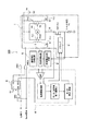
以下、本発明の実施形態を図面に基づいて説明する。図1は、本発明の一実施形態に係るパワーウインドウ駆動装置の構成を示すブロック図、図2は、具体的な構成を示す回路図(一部省略している)である。図1に示すように、該パワーウインドの駆動装置100は、ウインドガラスを駆動させるための駆動用モータM1を可逆的に回転駆動させるための駆動回路1と、参照電流生成回路2と、初期制御回路3と、基準電圧生成回路5、及び比較回路4を備えている。
Hereinafter, embodiments of the present invention will be described with reference to the drawings. FIG. 1 is a block diagram showing a configuration of a power window driving apparatus according to an embodiment of the present invention, and FIG. 2 is a circuit diagram (partially omitted) showing a specific configuration. As shown in FIG. 1, the power
更に、オア回路OR1と、フリップフロップ回路6、及び2つのアンド回路AND1,AND2を備えている。また、アンド回路AND1,AND2の出力端子は、それぞれFET(T11)、及びFET(T12)に接続されており、アンド回路AND1の出力信号が「H」レベルとなると、FET(T12)がオンとなり、アンド回路AND2の出力信号が「H」となると、FET(T11)がオンとなる。 Furthermore, an OR circuit OR1, a flip-flop circuit 6, and two AND circuits AND1 and AND2 are provided. The output terminals of the AND circuits AND1 and AND2 are connected to the FET (T11) and the FET (T12), respectively. When the output signal of the AND circuit AND1 becomes “H” level, the FET (T12) is turned on. When the output signal of the AND circuit AND2 becomes “H”, the FET (T11) is turned on.
駆動用モータM1は、2つのリレー接点RY1、RY2を介して、バッテリ電源VB、及びFET(T1)と接続され、更に、FET(T1)は、シャント抵抗Rsを介して、グランドに接続されている。 The drive motor M1 is connected to the battery power source VB and the FET (T1) via the two relay contacts RY1 and RY2, and the FET (T1) is connected to the ground via the shunt resistor Rs. Yes.
そして、ウインドガラスを上昇させるべくUp信号が入力されると、FET(T12)がオンとなり、リレー接点RY2がオンとなって、駆動用モータM1に順方向の電流が流れ、駆動用モータM1が順方向に回転して、ウインドガラスが上昇する。 When an Up signal is input to raise the window glass, the FET (T12) is turned on, the relay contact RY2 is turned on, a forward current flows through the driving motor M1, and the driving motor M1 is turned on. It rotates in the forward direction and the wind glass rises.
他方、ウインドガラスを下降させるべくDown信号が入力されると、FET(T11)がオンとなり、リレー接点RY1がオンとなって、駆動用モータM1に逆方向の電流が流れ、駆動用モータM1が逆方向に回転して、ウインドガラスが下降する。 On the other hand, when a Down signal is input to lower the window glass, the FET (T11) is turned on, the relay contact RY1 is turned on, a reverse current flows through the driving motor M1, and the driving motor M1 is turned on. Rotating in the opposite direction, the window glass descends.
また、駆動回路1は、ドライバ11を備えており、該ドライバ11により、FET(T1)のオン、オフが制御される。
Further, the drive circuit 1 includes a
図2に示すように、参照電流生成回路2は、2つのアンプAMP1,アンプAMP2と、2つのFET(T21),(T22)を備えている。アンプAMP1のマイナス側入力端子は、抵抗を介してFET(T1)とシャント抵抗Rsとの接続点(この点の電圧を、VSAとする)に接続され、プラス側入力端子は、抵抗を介して点P1(この点の電圧を、VSBとする)に接続されている。
As shown in FIG. 2, the reference
点P1は、抵抗R20を介してグランドに接続されている。なお、図2中、抵抗R20の下に記載した「300」とは、この抵抗R20が300Ωであることを示し、他の素子についても同様である。 The point P1 is connected to the ground via the resistor R20. In FIG. 2, “300” described under the resistor R20 indicates that the resistor R20 is 300Ω, and the same applies to other elements.
更に、点P1は、FET(T22)のドレイン、及びFET(T21)のドレインに接続され、FET(T22)のゲートは、アンプAMP1の出力端子に接続されている。また、FET(T22)のソース(点P4)は、抵抗R27、抵抗R24を介して、バッテリ電源VBに接続されている。 Further, the point P1 is connected to the drain of the FET (T22) and the drain of the FET (T21), and the gate of the FET (T22) is connected to the output terminal of the amplifier AMP1. The source (point P4) of the FET (T22) is connected to the battery power supply VB via the resistor R27 and the resistor R24.
また、抵抗R24と抵抗R27との接続点P2は、コンパレータCMP1のプラス側入力端子に接続されている。なお、点P2の電圧をVins(比較対象信号)とする。更に、点P4は後述するアンプAMP3のプラス側入力端子に接続されている。 The connection point P2 between the resistor R24 and the resistor R27 is connected to the plus side input terminal of the comparator CMP1. Note that the voltage at the point P2 is Vins (comparison target signal). Furthermore, the point P4 is connected to a plus side input terminal of an amplifier AMP3 described later.
FET(T21)のゲートは、アンプAMP2の出力端子に接続され、ソースは、抵抗R23を介してバッテリ電源VBに接続されている。アンプAMP2のマイナス側入力端子は、FET(T21)のソースに接続され、プラス側入力端子は、後述する初期制御回路3が有する抵抗R240に接続されている。
The gate of the FET (T21) is connected to the output terminal of the amplifier AMP2, and the source is connected to the battery power supply VB via the resistor R23. The negative input terminal of the amplifier AMP2 is connected to the source of the FET (T21), and the positive input terminal is connected to a resistor R240 included in the
初期制御回路3は、駆動用モータM1が起動した後、所定時間(例えば、50msec)オン状態となりその後オフとなるように動作する第1のタイマTM1と、同様に所定時間(例えば、200msec)オン状態となりその後オフとなるように動作する第2のタイマTM2と、FET(T41),(T42),(T241),(T240)を備えている。
The
第2のタイマTM2の出力端子は、FET(T42)のゲートに接続されており、該FET(T42)のソースは接地され、ドレインは、抵抗R242、R241を介して、バッテリ電源VBに接続されている。また、抵抗R242とR241との接続点は、FET(T241)のゲートに接続され、該FET(T241)のソースはバッテリ電源VBに接続されている。 The output terminal of the second timer TM2 is connected to the gate of the FET (T42), the source of the FET (T42) is grounded, and the drain is connected to the battery power supply VB via the resistors R242 and R241. ing. The connection point between the resistors R242 and R241 is connected to the gate of the FET (T241), and the source of the FET (T241) is connected to the battery power supply VB.
更に、FET(T241)のドレインは、抵抗R246、R247を介して、FET(T244)のソースに接続され、該FET(T244)のドレインは接地され、ゲートは点P4に接続されている。また、抵抗R247とFET(T244)との接続点は、コンデンサC24を介して接地されている。 Further, the drain of the FET (T241) is connected to the source of the FET (T244) via the resistors R246 and R247, the drain of the FET (T244) is grounded, and the gate is connected to the point P4. The connection point between the resistor R247 and the FET (T244) is grounded via the capacitor C24.
更に、抵抗R246とR247との接続点は、FET(T240;第2の半導体素子)のゲート(この点の電圧をVgとする)と接続され、該FET(T240)のドレインは、バッテリ電圧VBに接続され、ソースは抵抗R240(第2の抵抗)を介してアンプAMP2のプラス側入力端子と接続されると共に、後述する基準電圧生成回路5の、点P3とも接続されている。ここで、FET(T240)と、抵抗R240とにより、第2の回路が構成される。
Further, the connection point between the resistors R246 and R247 is connected to the gate (the voltage at this point is Vg) of the FET (T240; second semiconductor element), and the drain of the FET (T240) is connected to the battery voltage VB. The source is connected to the plus-side input terminal of the amplifier AMP2 via the resistor R240 (second resistor), and is also connected to the point P3 of the reference
第1のタイマTM1の出力端子は、FET(T41;第1の半導体素子)のゲートと接続され、該FET(T41)のソースは接地され、ドレインは、抵抗R42(第1の抵抗)を介して点P3に接続されている。ここで、FET(T41)と、抵抗R42とにより、第1の回路が構成される。 The output terminal of the first timer TM1 is connected to the gate of an FET (T41; first semiconductor element), the source of the FET (T41) is grounded, and the drain is connected via a resistor R42 (first resistor). Connected to point P3. Here, the FET (T41) and the resistor R42 constitute a first circuit.
基準電圧生成回路5は、電流源IA、IBと、アンプAMP3とコンデンサC1を備えている。アンプAMP3のプラス側入力端子は、前述した点P4と接続され、点P4における電圧Vc2が印加される。また、マイナス側入力端子(点P3)は、コンデンサC1を介して電源電圧VBと接続され、且つ、この点P3は、比較回路4が有するコンパレータCMP1のマイナス側入力端子に接続されている。
The reference
電流源IA、IBの電流値はIB=2*IAの関係を満足するように構成され、バッテリ電源VBとグランドとの間に直列接続されており、その接続点が点P3となっている。また、電流源IBは、アンプAMP3の出力端子が「L」レベルのときに電流を流し、「H」レベルのときに電流を停止する。 The current values of the current sources IA and IB are configured to satisfy the relationship of IB = 2 * IA, and are connected in series between the battery power supply VB and the ground, and the connection point is a point P3. The current source IB allows a current to flow when the output terminal of the amplifier AMP3 is at the “L” level, and stops the current when the output terminal is at the “H” level.
この際、電圧Vc2>Vcであれば、アンプAMP3の出力信号がHレベルとなって、定電流源IBは遮断され、コンデンサC1のマイナス側入力端子には、電流IAが流れ込んで電圧Vc(基準電圧信号)は上昇する。また、電圧Vc2<Vcであれば、アンプAMP3の出力信号がLレベルとなり、電流IBが流れ、コンデンサC1のマイナス側端子から(IB−IA)=IAの電流が引き出され、電圧Vcは低下する。 At this time, if the voltage Vc2> Vc, the output signal of the amplifier AMP3 becomes H level, the constant current source IB is cut off, and the current IA flows into the negative side input terminal of the capacitor C1, and the voltage Vc (reference Voltage signal) rises. If the voltage Vc2 <Vc, the output signal of the amplifier AMP3 becomes L level, the current IB flows, the current of (IB−IA) = IA is drawn from the negative terminal of the capacitor C1, and the voltage Vc decreases. .
なお、図2では、図1に示したコンパレータCMP1の出力側に設けられる電流制限回路、モータ回転数低下量検出回路、モータ停止・反転回路、及びドライバーを、省略して記載している。 In FIG. 2, the current limiting circuit, the motor rotation speed decrease detection circuit, the motor stop / inversion circuit, and the driver provided on the output side of the comparator CMP1 shown in FIG. 1 are omitted.
次に、上述のように構成された本実施形態に係るパワーウインドの駆動装置の動作について説明する。パワーウインド起動時には、駆動用モータM1に流れる電流が、図3の曲線S1にように変化する。つまり、起動直後に電流値が急増し、その後、電流値が低減し、再度上昇しながら(図中X1に示す部分)、定常電流に安定する。 Next, the operation of the power window driving apparatus according to the present embodiment configured as described above will be described. When the power window is activated, the current flowing through the drive motor M1 changes as shown by a curve S1 in FIG. That is, immediately after startup, the current value increases rapidly, and then the current value decreases and rises again (portion indicated by X1 in the figure) while stabilizing to a steady current.
本実施形態では、起動後50msec程度まで発生する突入電流による誤動作、及び起動後50〜200msec程度(図中X1に示す範囲)で発生する電流変動に起因する誤作動を防止し、且つ、ウインドガラスが障害物を挟み込んだ場合には、確実にこれを検知する。 In the present embodiment, malfunction due to an inrush current occurring up to about 50 msec after startup, and malfunction due to current fluctuation occurring in about 50 to 200 msec (range indicated by X1 in the figure) after startup are prevented. If an obstacle is caught, this is surely detected.
まず、通常時の動作について説明する。図1に示すUp信号が入力されると、アンド回路AND1の出力信号が「H」レベルとなり、FET(T12)がオンとなる。これにより、リレー設定RY2がオンとなり、バッテリ電源VB、リレー接点RY2、駆動用モータM1、リレー接点RY1、FET(T1)、シャント抵抗Rsの順で電流が流れ、駆動用モータM1が駆動して、ウインドガラスが上昇方向に駆動する。 First, the normal operation will be described. When the Up signal shown in FIG. 1 is input, the output signal of the AND circuit AND1 becomes “H” level, and the FET (T12) is turned on. As a result, the relay setting RY2 is turned on, current flows in the order of the battery power source VB, the relay contact RY2, the drive motor M1, the relay contact RY1, the FET (T1), and the shunt resistor Rs, and the drive motor M1 is driven. The wind glass is driven in the upward direction.
この際、シャント抵抗Rsの両端には、駆動用モータM1のモータ電流IDに比例した大きさの電圧が発生し、この電圧がVSAとなる。また、参照電流生成回路2の抵抗R20には、FET(T22)に流れる電流Ir1(第1の電流)と、FET(T21)に流れる電流Ir3(第2の電流)とを足し合わせた参照電流Irが流れており、この抵抗R20の両端には、参照電流Irに比例した大きさの電圧が発生し、この電圧がVSBとなる。
At this time, a voltage in proportion to the motor current ID of the driving motor M1 is generated at both ends of the shunt resistor Rs, and this voltage becomes VSA. Further, the resistor R20 of the reference
そして、アンプAMP1の出力信号は、電圧VSAと電圧VSBとの差分に比例した大きさとなり、この出力信号がFET(T22)のゲートに供給されるので、モータ電流IDに比例した大きさの参照電流Irとなるように、電流Ir1が制御される。この電流Ir1の大きさは、点P2における電圧Vinsに反映されるので、モータ電流IDが正常な値であれば(急激な電流増加がなければ)、電圧Vinsは、点P3にて発生する基準電圧Vcよりも大きくなり、コンパレータCMP1の出力信号が、通常状態を示す「H」レベルとなる。従って、比較回路4による駆動用モータM1の停止・反転動作は行われない。 The output signal of the amplifier AMP1 has a magnitude proportional to the difference between the voltage VSA and the voltage VSB, and since this output signal is supplied to the gate of the FET (T22), a reference proportional to the motor current ID is made. The current Ir1 is controlled so as to be the current Ir. Since the magnitude of the current Ir1 is reflected in the voltage Vins at the point P2, if the motor current ID is a normal value (unless there is a sudden increase in current), the voltage Vins is a reference generated at the point P3. The voltage becomes higher than the voltage Vc, and the output signal of the comparator CMP1 becomes “H” level indicating a normal state. Therefore, the stop / reverse operation of the drive motor M1 by the comparison circuit 4 is not performed.
また、駆動用モータM1に急激な電流増加が発生すると、これに伴って、参照電流Irが増大し、抵抗R24による電圧降下分が大きくなるので、点P2における電圧Vinsが低下して、基準電圧Vcを下回ることになる。すると、コンパレータCMP1の出力信号が反転して「L」レベルとなり、ドライバ回路11によりFET(T1)がオフとされる。また、比較回路4がフリップフロップ回路6にリセット信号を出力し、アンド回路AND1,AND2への出力信号を「L」レベルに切り換える。これにより、駆動用モータM1は停止する。
Further, when a sudden current increase occurs in the drive motor M1, the reference current Ir increases accordingly, and the voltage drop due to the resistor R24 increases, so the voltage Vins at the point P2 decreases and the reference voltage It will be below Vc. Then, the output signal of the comparator CMP1 is inverted and becomes “L” level, and the
これにより、ウインドガラスが上昇しているときに、障害物を挟み込み、駆動用モータM1に過電流が流れた場合には、駆動用モータM1を即時に停止させることができ、障害物の損傷或いはウインドガラス自体の損傷を防止することができる。 As a result, when an obstacle is caught when the window glass is rising and an overcurrent flows through the driving motor M1, the driving motor M1 can be stopped immediately, and the obstacle can be damaged or It is possible to prevent damage to the window glass itself.
次に、駆動用モータM1を駆動させた直後の動作について説明する。駆動直後においては、図2に示した第1のタイマTM1、第2のタイマTM2の出力信号が共に「H」レベルとなる。 Next, an operation immediately after driving the driving motor M1 will be described. Immediately after driving, the output signals of the first timer TM1 and the second timer TM2 shown in FIG. 2 are both at the “H” level.
また、駆動用モータM1の起動直後(特に、下降動作を行った後に初めて上昇させる場合)には、駆動用モータM1は一時的に無負荷状態となり、その後、負荷がかかるので、大きな電流変化が発生する。本実施形態では、この電流変化に起因する誤停止の発生を防止し、且つ、真の挟み込みが発生した場合には、これを確実に検知するように動作する。 Immediately after the driving motor M1 is started (especially when it is raised for the first time after performing the lowering operation), the driving motor M1 is temporarily in a no-load state and then loaded, so that a large current change occurs. appear. In the present embodiment, the operation is performed so as to prevent the erroneous stop due to the current change and to detect this surely when the true pinching occurs.
第1のタイマTM1がオンとなると、FET(T41)のゲートに「H」レベルの信号が供給されて、該FET(T41)がオンとなる。 When the first timer TM1 is turned on, an “H” level signal is supplied to the gate of the FET (T41), and the FET (T41) is turned on.
第2のタイマTM2がオンの場合には、FET(T42)のゲートに第2のタイマTM2の出力信号が供給され、該FET(T42)がオンとなる。これにより、FET(T241)がオンとなり、FET(T240)及び抵抗R240からなる第2の回路を作動させる。 When the second timer TM2 is on, the output signal of the second timer TM2 is supplied to the gate of the FET (T42), and the FET (T42) is turned on. As a result, the FET (T241) is turned on, and the second circuit including the FET (T240) and the resistor R240 is operated.
FET(T240)のゲートには、点P2における電圧Vinsから派生した電圧Vgが印加される。この電圧Vgは、FET(T244)、抵抗R246,R247、及びコンデンサC24からなる回路により、以下に示すように生成される。 A voltage Vg derived from the voltage Vins at the point P2 is applied to the gate of the FET (T240). This voltage Vg is generated as shown below by a circuit comprising an FET (T244), resistors R246 and R247, and a capacitor C24.
抵抗R246、R247、FET(T244)が直列に接続され、抵抗R246の一方の端子がFET(T241)のドレインに接続され、抵抗R246とR247との結合点が、FET(T240)のゲートに接続されている。 Resistors R246, R247 and FET (T244) are connected in series, one terminal of resistor R246 is connected to the drain of FET (T241), and the junction of resistors R246 and R247 is connected to the gate of FET (T240) Has been.
FET(T244)のドレインを接地し、このゲートに、参照電流生成手段2で生成された、点P4の電圧Vc2を印加する。 The drain of the FET (T244) is grounded, and the voltage Vc2 at the point P4 generated by the reference current generating means 2 is applied to this gate.
FET(T241)がオンしているとき(即ち、タイマTM2がオンのとき)、FET(T244)と抵抗(R246+R247)はソースフォロアとして動作する。FET(T240)のゲート電圧をVgとし、FET(T244)のスレッショルド電圧をVth244とすると、以下に示す(1)式が成立する。 When the FET (T241) is on (that is, when the timer TM2 is on), the FET (T244) and the resistor (R246 + R247) operate as a source follower. When the gate voltage of the FET (T240) is Vg and the threshold voltage of the FET (T244) is Vth244, the following equation (1) is established.
Vg=Vc2+Vth244
+(VB−Vth244−Vc2)×R247/(R246+R247)…(1)
一方、比較対象信号Vinsを電圧VB、及びVc2を用いて表すと、以下に示す(2)式が得られる。
Vg = Vc2 + Vth244
+ (VB−Vth244−Vc2) × R247 / (R246 + R247) (1)
On the other hand, when the comparison target signal Vins is expressed using the voltages VB and Vc2, the following equation (2) is obtained.
Vins=Vc2+(VB−Vc2)*R27/(R24+R27) …(2)
VinsとVgの電位差を、ΔVinsgとし、(2)式の両辺から(1)式の両辺を減じると、以下の(3)式が得られる。
Vins = Vc2 + (VB−Vc2) * R27 / (R24 + R27) (2)
When the potential difference between Vins and Vg is ΔVinsg and both sides of equation (1) are subtracted from both sides of equation (2), the following equation (3) is obtained.
ΔVinsg=Vins−Vg
=(VB−Vc2)*{R27/(R24+R27)
−R247/(R246+R247)}
−Vth244*{1−R247/(R246+R247)} …(3)
FET(T240)のスレッショルド電圧をVth240とし、比較対象信号VinsとFET(T240)ソース間の電位差をVclmpとすると、以下の(4)式が得られる。
ΔVinsg = Vins−Vg
= (VB-Vc2) * {R27 / (R24 + R27)
-R247 / (R246 + R247)}
-Vth244 * {1-R247 / (R246 + R247)} (3)
When the threshold voltage of the FET (T240) is Vth240 and the potential difference between the comparison target signal Vins and the source of the FET (T240) is Vclmp, the following equation (4) is obtained.
Vclmp=ΔVinsg+Vth240
=(VB−Vc2)*{R27/(R24+R27)
−R247/(R246+R247)}
−Vth244*{1−R247/(R246+R247)}
+Vth240 …(4)
ここで、Vth240=Vth244となるようにFET(T240)、FET(T244)のスレッショルド電圧を選定すると、以下の(5)式が得られる。
Vclmp = ΔVinsg + Vth240
= (VB-Vc2) * {R27 / (R24 + R27)
-R247 / (R246 + R247)}
-Vth244 * {1-R247 / (R246 + R247)}
+ Vth240 (4)
Here, when the threshold voltages of the FET (T240) and the FET (T244) are selected so that Vth240 = Vth244, the following expression (5) is obtained.
Vclmp=(VB−Vc2)*{R27/(R24+R27)
−R247/(R246+R247)}
+Vth240*R247/(R246+R247) … (5)
図2に示した例では、R24=14KΩ、R27=8.5KΩ、R246=560KΩ、R247=270KΩ、Vth=0.85Vに設定しているので、以下の(6)式が得られる。
Vclmp = (VB−Vc2) * {R27 / (R24 + R27)
-R247 / (R246 + R247)}
+ Vth240 * R247 / (R246 + R247) (5)
In the example shown in FIG. 2, since R24 = 14 KΩ, R27 = 8.5 KΩ, R246 = 560 KΩ, R247 = 270 KΩ, and Vth = 0.85 V, the following equation (6) is obtained.
Vclmp=0.052*(VB−Vc2)+0.276(V) … (6)
ここで、FET(T244)のソースとグランド間にコンデンサC24を設置している。コンデンサC24の放電は、FET(T244)を通して行われるので、放電抵抗は非常に小さい。一方、コンデンサC24の充電は抵抗値の大きい抵抗(R246+R247)を通して行われるので、その時定数は大きくなる。
Vclmp = 0.052 * (VB−Vc2) +0.276 (V) (6)
Here, a capacitor C24 is installed between the source of the FET (T244) and the ground. Since the capacitor C24 is discharged through the FET (T244), the discharge resistance is very small. On the other hand, since the capacitor C24 is charged through a resistor (R246 + R247) having a large resistance value, the time constant becomes large.
図2に示す回路では、R246=560KΩ、R247=270KΩ、C24=0.01μFとしているので、充電時定数は8.3msecとなる。従って、Vc2が脈動成分により変動したとき、その最小値に対応した電圧レベルに、FET(T244)のソースが保持される。 In the circuit shown in FIG. 2, since R246 = 560 KΩ, R247 = 270 KΩ, and C24 = 0.01 μF, the charging time constant is 8.3 msec. Therefore, when Vc2 fluctuates due to the pulsation component, the source of the FET (T244) is held at the voltage level corresponding to the minimum value.
電圧Vinsも、電圧Vc2に同期して脈動するので、電圧Vinsの最小値に対して、Vcをクランプしていることになる。挟み込み検出の閾値電圧(これを、Vjthとする)は、電圧Vinsの最小値とVcとの電位差になるので、閾値電圧Vjthに対応したクランプ電圧が実現していることになる。 Since the voltage Vins also pulsates in synchronization with the voltage Vc2, Vc is clamped with respect to the minimum value of the voltage Vins. Since the threshold voltage for pinching detection (this is referred to as Vjth) is a potential difference between the minimum value of the voltage Vins and Vc, a clamp voltage corresponding to the threshold voltage Vjth is realized.
次に、上記の内容を踏まえて、駆動用モータM1の起動直後の動作について説明する。駆動用モータM1を起動すると、第1のタイマTM1、及び第2のタイマTM2が共にスタートする。第1のタイマTM1の出力信号が「H」レベルとなることにより、FET(T41)、FET(T42)が共にオンとなり、第1の回路(T41,R42からなる回路)、及び第2の回路(T240,R240からなる回路)が同時に作動する。その結果、抵抗R240、及びR42に電流Ir4が流れ、点P3における電圧Vcは(Vins−Vclmp)を、抵抗R240とR42で分圧した電圧、即ち、(Vins−Vclmp)*R42/(R42+R240)に保持される。このときの比較対象信号Vinsは、基準電圧信号Vcよりも大きく、比較対象信号Vinsと基準電圧信号Vcの差は、以下の(7)式にて示すことができる。 Next, based on the above contents, the operation immediately after the drive motor M1 is activated will be described. When the driving motor M1 is activated, both the first timer TM1 and the second timer TM2 are started. When the output signal of the first timer TM1 becomes “H” level, both the FET (T41) and the FET (T42) are turned on, and the first circuit (the circuit composed of T41 and R42), and the second circuit (Circuit consisting of T240 and R240) operate simultaneously. As a result, the current Ir4 flows through the resistors R240 and R42, and the voltage Vc at the point P3 is a voltage obtained by dividing (Vins−Vclmp) by the resistors R240 and R42, that is, (Vins−Vclmp) * R42 / (R42 + R240). Retained. The comparison target signal Vins at this time is larger than the reference voltage signal Vc, and the difference between the comparison target signal Vins and the reference voltage signal Vc can be expressed by the following equation (7).
Vins−Vc=(Vins−Vclmp)*R240/(R240+R42)+Vclmp…(7)
その結果、2つの電圧の間には、一定値以上の電圧差が確保される。(7)式で示した電圧「Vins−Vc」が、第1の所定値である。
Vins−Vc = (Vins−Vclmp) * R240 / (R240 + R42) + Vclmp (7)
As a result, a voltage difference of a certain value or more is ensured between the two voltages. The voltage “Vins−Vc” expressed by the equation (7) is the first predetermined value.
従って、駆動用モータM1を駆動開始した後、タイマTM1の出力信号がオフとなるまで(例えば、50msecが経過するまで)の間は、第1の所定値((7)式に示す電圧)により、電圧Vinsが基準電圧Vcを下回ることを防止することができ、駆動開始時における突入電流により、駆動用モータM1の回転動作が停止するというトラブルを回避することができる。 Therefore, after the drive motor M1 is started to drive until the output signal of the timer TM1 is turned off (for example, until 50 msec elapses), the first predetermined value (the voltage shown in the equation (7)) is used. The voltage Vins can be prevented from falling below the reference voltage Vc, and the trouble that the rotational operation of the driving motor M1 stops due to the inrush current at the start of driving can be avoided.
その後、第1のタイマTM1がオフとなると(50msecが経過すると)、FET(T41)がオフとなり、電流Ir4は、コンデンサC1を充電する電流のみとなるので、該電流Ir4は急速に減少し、電圧Vinsと電圧Vcとの間の電位差は単調減少することになる。そのときの減少勾配は、「C1*R240」の大きさで規制されることになる。 After that, when the first timer TM1 is turned off (when 50 msec has elapsed), the FET (T41) is turned off, and the current Ir4 is only the current for charging the capacitor C1, so that the current Ir4 decreases rapidly, The potential difference between the voltage Vins and the voltage Vc decreases monotonously. The decreasing gradient at that time is regulated by the magnitude of “C1 * R240”.
コンデンサC1の充電が終了して、電流Ir4が零となると、電圧Vinsと電圧Vcとの間の電位差は、Vclmpに収束する。Vclmpが第2の所定値である。 When the charging of the capacitor C1 is finished and the current Ir4 becomes zero, the potential difference between the voltage Vins and the voltage Vc converges to Vclmp. Vclmp is a second predetermined value.
従って、図3の符号X1に示した領域では、電圧Vinsと電圧Vcとの間に電圧Vclmpが生じるので、通常動作による電流の増加(領域X1に示す電流増加)では、コンパレータCMP1の出力が反転することなく、「H」レベルを維持する。また、障害物の挟み込みにより、駆動用モータM1に流れるモータ電流IDが増加し、電圧Vinsが基準電圧Vcを下回ると、コンパレータCMP1の出力信号が反転して、「L」レベルとなるので、図1に示したドライバ11の制御により、FET(T1)をオフとし、駆動用モータM1を停止させる。但し、第2の所定値Vclmpを大きく設定すると誤反転防止効果は強まるが、挟み込み発生時の反転荷重は増大する。逆に、第2の所定値を小さくすると反転荷重は低下するが、図3の符号X1に示す電流変化に対する誤反転防止効果も低下するので、これらを考慮して、TM1、TM2、時定数C1*R240を設定する必要がある。
Therefore, in the region indicated by reference numeral X1 in FIG. 3, the voltage Vclmp is generated between the voltage Vins and the voltage Vc. Therefore, when the current increases due to normal operation (current increase indicated by the region X1), the output of the comparator CMP1 is inverted. Without maintaining, the “H” level is maintained. Further, when the obstacle is caught, the motor current ID flowing through the driving motor M1 increases, and when the voltage Vins falls below the reference voltage Vc, the output signal of the comparator CMP1 is inverted and becomes “L” level. Under the control of the
こうして、駆動用モータM1の起動開始後、一旦低下して再度上昇する電流による誤停止を防止することができ、且つ、この時間帯で挟み込みが発生した場合には確実にこれを検知し、駆動用モータM1を停止させることができるのである。 In this way, it is possible to prevent an erroneous stop due to a current that once decreases and then increases again after the start of the driving motor M1, and when the jamming occurs in this time zone, this is surely detected and driven. The motor M1 can be stopped.
このようにして、本実施形態に係るパワーウインドの駆動装置100では、駆動用モータM1の駆動を開始した際に、駆動開始後第1のタイマTM1で計時される時間が経過するまでの間(例えば、50msec)は、第1の所定値で設定される電位差が、電圧Vinsと電圧Vcとの間に発生するので、駆動時に発生する突入電流により、駆動用モータM1が停止するというトラブルを回避することができる。
In this way, in the power
また、第1のタイマTM1による計時が終了し、第2のタイマTM2による計時が継続している間(例えば、駆動開始後50〜200msecの間)は、第2の所定値(Vclmp)で設定される電位差が、電圧Vinsと電圧Vcとの間に発生するので、駆動初期に生じる電流の上昇(図3の符号X1に示す電流上昇)が発生した場合に、駆動用モータM1が誤停止するというトラブルを回避することができ、且つ、挟み込みが発生した場合には、確実にこれを検知して駆動用モータM1を停止させることができる。 Further, while the time measurement by the first timer TM1 ends and the time measurement by the second timer TM2 continues (for example, for 50 to 200 msec after the start of driving), the second predetermined value (Vclmp) is set. Since the potential difference generated is generated between the voltage Vins and the voltage Vc, the drive motor M1 erroneously stops when a current increase (current increase indicated by reference numeral X1 in FIG. 3) that occurs in the initial stage of driving occurs. In addition, when the jam occurs, it is possible to reliably detect this and stop the driving motor M1.
以上、本発明のパワーウインドの駆動装置を図示の実施形態に基づいて説明したが、本発明はこれに限定されるものではなく、各部の構成は、同様の機能を有する任意の構成のものに置き換えることができる。例えば、上記した実施形態では、第1のタイマTM1の計時時間を50msec、第2のタイマTM2の計時時間を200msecに設定する例を挙げたが、本発明はこれに限定されるものではなく、駆動用モータM1の特性に応じて、適切な時間を設定することができる。 As mentioned above, although the drive device of the power window of this invention was demonstrated based on embodiment of illustration, this invention is not limited to this, The structure of each part is set to the thing of the arbitrary structures which have the same function. Can be replaced. For example, in the above-described embodiment, an example is given in which the time measurement of the first timer TM1 is set to 50 msec and the time measurement of the second timer TM2 is set to 200 msec, but the present invention is not limited to this. An appropriate time can be set according to the characteristics of the driving motor M1.
パワーウインドの挟み込みを防止する上で、極めて有用である。 It is extremely useful for preventing the power window from being caught.
1 駆動回路
2 参照電流生成回路
3 初期制御回路
4 比較回路
5 基準電圧生成回路
6 フリップフロップ回路
11 ドライバ
100 パワーウインドの駆動装置
M1 駆動用モータ
DESCRIPTION OF SYMBOLS 1
M1 drive motor
Claims (6)
前記駆動用モータに流れるモータ電流(ID)の大きさに対応したレベルとなる参照電流(Ir)を生成する参照電流生成手段を有し、
前記参照電流生成手段は、前記モータ電流(ID)の変動値に対応したレベルとなる第1の電流(Ir1)を生成する第1の電流生成手段と、
前記第1の電流を電圧に変換し、これを第1の電圧(Vc2)とするとき、第1の電圧の時間的な平均値から生成される基準電圧(Vc)と、
前記基準電圧(Vc)から生成した電流で、前記第1の電流(Ir1)と足し合わせることにより参照電流(Ir)に等しくなる大きさとなる第2の電流(Ir3)を生成する第2の電流生成手段を備え、且つ、前記第1の電流を電圧に変換した電圧で、前記第1の電圧(Vc2)よりも大きい電圧である比較対象信号(Vins)を生成し、
前記比較対象信号(Vins)と基準電圧信号(Vc)とを比較する比較手段(CMP1)と、
前記比較手段による比較結果に基づき、前記駆動用モータに流れる電流に急峻な電流増加が発生したと判断された際に、前記駆動用モータを停止、或いは反転させる停止反転手段と、
前記駆動用モータを起動した際には、起動開始からの2つの所定時間を計測する第1のタイマ(TM1)、及び第2のタイマ(TM2)とを有し、
前記第1のタイマが作動している間、前記比較対象信号(Vins)が前記基準電圧信号(Vc)よりも大きい状態で、且つ、前記比較対象信号と基準電圧の差が第1の所定値以上になるように保持し、
前記第1のタイマによる計時が終了した後、前記第2のタイマが作動している間には、前記比較対象信号と基準電圧信号の差が第2の所定値(Vclmp)となるまで単調減少させることを特徴とするパワーウインドの駆動装置。 In a power window drive device that controls the drive of a power window mounted on a vehicle,
A reference current generating means for generating a reference current (Ir) having a level corresponding to the magnitude of the motor current (ID) flowing through the driving motor;
The reference current generating means generates first current (Ir1) having a level corresponding to a fluctuation value of the motor current (ID),
When the first current is converted into a voltage and this is used as the first voltage (Vc2), a reference voltage (Vc) generated from a temporal average value of the first voltage;
A second current that generates a second current (Ir3) having a magnitude equal to the reference current (Ir) by adding the first current (Ir1) with the current generated from the reference voltage (Vc). Generating a comparison target signal (Vins) which is a voltage obtained by converting the first current into a voltage and is larger than the first voltage (Vc2);
A comparison means (CMP1) for comparing the signal to be compared (Vins) with a reference voltage signal (Vc);
Stop reversing means for stopping or reversing the driving motor when it is determined that a steep current increase has occurred in the current flowing through the driving motor based on the comparison result by the comparing means ;
When turning on the pre-SL drive motor, a first timer for measuring the two predetermined time from the start initiation (TM1), and a second timer (TM2),
While the first timer is operating, the comparison target signal (Vins) is larger than the reference voltage signal (Vc), and the difference between the comparison target signal and the reference voltage is a first predetermined value. Hold to be more,
After the time measurement by the first timer is completed, while the second timer is operating, it decreases monotonically until the difference between the comparison target signal and the reference voltage signal becomes a second predetermined value (Vclmp). A drive device for a power window, characterized in that
前記基準電圧信号とグランドレベルとの間に第1の抵抗(R42)と第1の半導体素子(T41)の直列接続からなる第1の回路を有し、
前記第1のタイマが作動している間、第1の半導体素子を導通させることにより実現することを特徴とする請求項2に記載のパワーウインドの駆動装置。 While the first timer is operating, the difference between the comparison target signal and the reference voltage signal is greater than or equal to the first predetermined value in a state where the comparison target signal is larger than the reference voltage signal. The means to hold in
A first circuit comprising a series connection of a first resistor (R42) and a first semiconductor element (T41) between the reference voltage signal and the ground level;
3. The power window driving device according to claim 2, wherein the power window driving device is realized by conducting the first semiconductor element while the first timer is operating.
第2の半導体素子(T240)と、第2の抵抗(R240)との直列接続からなる第2の回路を、電源電圧と基準電圧信号との間に設置し、
第2の半導体素子の制御電極に比較対象信号、または比較対象信号に所定の電圧を加算または減算した電圧を印加することを特徴とする請求項2に記載のパワーウインドの駆動装置。 Means for monotonously decreasing the difference between the comparison target signal and the reference voltage signal to a second predetermined value while the second timer is operating after the time measurement by the first timer is completed. ,
A second circuit comprising a series connection of a second semiconductor element (T240) and a second resistor (R240) is installed between the power supply voltage and the reference voltage signal;
3. The power window driving device according to claim 2, wherein a comparison target signal or a voltage obtained by adding or subtracting a predetermined voltage to the comparison target signal is applied to the control electrode of the second semiconductor element.
Priority Applications (4)
| Application Number | Priority Date | Filing Date | Title |
|---|---|---|---|
| JP2003341803A JP3964375B2 (en) | 2003-09-30 | 2003-09-30 | Power window drive |
| CNB2004100832108A CN100365933C (en) | 2003-09-30 | 2004-09-29 | Electric window drive apparatus |
| DE102004047688A DE102004047688A1 (en) | 2003-09-30 | 2004-09-30 | Drive device for windows with electric windows |
| US10/953,444 US6954043B2 (en) | 2003-09-30 | 2004-09-30 | Power window driving apparatus |
Applications Claiming Priority (1)
| Application Number | Priority Date | Filing Date | Title |
|---|---|---|---|
| JP2003341803A JP3964375B2 (en) | 2003-09-30 | 2003-09-30 | Power window drive |
Publications (3)
| Publication Number | Publication Date |
|---|---|
| JP2005110429A JP2005110429A (en) | 2005-04-21 |
| JP2005110429A5 JP2005110429A5 (en) | 2007-04-19 |
| JP3964375B2 true JP3964375B2 (en) | 2007-08-22 |
Family
ID=34536297
Family Applications (1)
| Application Number | Title | Priority Date | Filing Date |
|---|---|---|---|
| JP2003341803A Expired - Fee Related JP3964375B2 (en) | 2003-09-30 | 2003-09-30 | Power window drive |
Country Status (4)
| Country | Link |
|---|---|
| US (1) | US6954043B2 (en) |
| JP (1) | JP3964375B2 (en) |
| CN (1) | CN100365933C (en) |
| DE (1) | DE102004047688A1 (en) |
Families Citing this family (10)
| Publication number | Priority date | Publication date | Assignee | Title |
|---|---|---|---|---|
| DE102004008394A1 (en) * | 2004-02-20 | 2005-09-08 | Siemens Ag | Device and method for driving an arranged in the shunt arm of a bridge circuit electric motor |
| US20060066274A1 (en) * | 2004-09-30 | 2006-03-30 | Valeo Electrical Systems, Inc. | Overmodulation of electric motor in power steering system |
| JP6164429B2 (en) | 2012-05-01 | 2017-07-19 | 大島俊蔵 | Overcurrent protection power supply |
| KR101462112B1 (en) * | 2014-02-28 | 2014-11-17 | 동양기전 주식회사 | Apparatus and method for controlling power window using output currents of motor |
| CN104155502B (en) * | 2014-08-29 | 2017-01-25 | 北京经纬恒润科技有限公司 | Voltage fluctuation detection method and system |
| JP2016127573A (en) * | 2015-01-08 | 2016-07-11 | 株式会社東芝 | Analog switch and multiplexer |
| CN104883101B (en) * | 2015-05-06 | 2018-10-19 | 青岛歌尔声学科技有限公司 | A kind of DC motor rotation speed control circuit and electronic equipment with the circuit |
| WO2017134824A1 (en) | 2016-02-05 | 2017-08-10 | 俊蔵 大島 | Power supply device |
| JP6491302B1 (en) * | 2017-12-07 | 2019-03-27 | 東芝エレベータ株式会社 | Elevator door control device and elevator door control method |
| CN111155866A (en) * | 2020-01-08 | 2020-05-15 | 温州医科大学 | Control system and method of photoinduction automatic window |
Family Cites Families (6)
| Publication number | Priority date | Publication date | Assignee | Title |
|---|---|---|---|---|
| JP3553280B2 (en) * | 1996-07-11 | 2004-08-11 | オムロン株式会社 | Power window switch device |
| JP2000179230A (en) * | 1998-12-18 | 2000-06-27 | Yazaki Corp | Opening and closing drive control device |
| JP2001020605A (en) * | 1999-07-09 | 2001-01-23 | Yazaki Corp | Power window device |
| JP2002096632A (en) | 2000-09-21 | 2002-04-02 | Yazaki Corp | Insertion detection device and window controller |
| JP4287070B2 (en) * | 2001-04-02 | 2009-07-01 | 矢崎総業株式会社 | Power window prevention device |
| US6630807B2 (en) * | 2001-04-27 | 2003-10-07 | Daimlerchrysler Corporation | Convertible power top control system |
-
2003
- 2003-09-30 JP JP2003341803A patent/JP3964375B2/en not_active Expired - Fee Related
-
2004
- 2004-09-29 CN CNB2004100832108A patent/CN100365933C/en not_active Expired - Fee Related
- 2004-09-30 US US10/953,444 patent/US6954043B2/en not_active Expired - Fee Related
- 2004-09-30 DE DE102004047688A patent/DE102004047688A1/en not_active Withdrawn
Also Published As
| Publication number | Publication date |
|---|---|
| US20050104546A1 (en) | 2005-05-19 |
| CN100365933C (en) | 2008-01-30 |
| US6954043B2 (en) | 2005-10-11 |
| DE102004047688A1 (en) | 2005-08-11 |
| CN1604473A (en) | 2005-04-06 |
| JP2005110429A (en) | 2005-04-21 |
Similar Documents
| Publication | Publication Date | Title |
|---|---|---|
| US8054605B2 (en) | Power supply controller | |
| JP3964375B2 (en) | Power window drive | |
| US7852024B2 (en) | Vehicle mirror device | |
| WO2015064002A1 (en) | Controlling device and control method for vehicle opening and closing body and vehicle opening and closing body comprising same controlling device | |
| JP4344569B2 (en) | Power window drive | |
| US6838850B2 (en) | Method for controlling motorized storing door mirror | |
| US6531840B2 (en) | Power window apparatus provided with control part for detecting pinching and method for controlling the same | |
| JPH06327279A (en) | Electrically driven device | |
| JPH08251982A (en) | Motor controller | |
| EP3982540B1 (en) | Switch control device, switch control method, and in-vehicle power supply system | |
| JP4148243B2 (en) | Abnormality detection circuit | |
| JPH07255198A (en) | Motor controller | |
| JP3188806B2 (en) | DC motor rotation failure detection device and DC motor drive device | |
| JP2002227521A (en) | Bite detecting device for window glass | |
| JP3774144B2 (en) | Power window control device with anti-pinch function | |
| JPH08254070A (en) | Control device of power window regulator for car | |
| JPS6332756Y2 (en) | ||
| JP2004244907A (en) | Driving device of power window | |
| JP2001098844A (en) | Power window controller for vehicle | |
| JP3831129B2 (en) | Electric motor drive | |
| JPH03245772A (en) | Charge protective circuit for capacitor | |
| JP2002168049A (en) | Detection device for existence of insertion of window glass | |
| JPH0947080A (en) | Motor controller | |
| JP2007327220A (en) | Power window device | |
| JP3624176B2 (en) | Power window drive control device |
Legal Events
| Date | Code | Title | Description |
|---|---|---|---|
| A621 | Written request for application examination |
Free format text: JAPANESE INTERMEDIATE CODE: A621 Effective date: 20060126 |
|
| A977 | Report on retrieval |
Free format text: JAPANESE INTERMEDIATE CODE: A971007 Effective date: 20070227 |
|
| A521 | Request for written amendment filed |
Free format text: JAPANESE INTERMEDIATE CODE: A523 Effective date: 20070301 |
|
| A131 | Notification of reasons for refusal |
Free format text: JAPANESE INTERMEDIATE CODE: A131 Effective date: 20070306 |
|
| TRDD | Decision of grant or rejection written | ||
| A01 | Written decision to grant a patent or to grant a registration (utility model) |
Free format text: JAPANESE INTERMEDIATE CODE: A01 Effective date: 20070515 |
|
| A61 | First payment of annual fees (during grant procedure) |
Free format text: JAPANESE INTERMEDIATE CODE: A61 Effective date: 20070523 |
|
| R150 | Certificate of patent or registration of utility model |
Free format text: JAPANESE INTERMEDIATE CODE: R150 |
|
| LAPS | Cancellation because of no payment of annual fees |