JP3962484B2 - Liquid crystal device - Google Patents
Liquid crystal device Download PDFInfo
- Publication number
- JP3962484B2 JP3962484B2 JP17937198A JP17937198A JP3962484B2 JP 3962484 B2 JP3962484 B2 JP 3962484B2 JP 17937198 A JP17937198 A JP 17937198A JP 17937198 A JP17937198 A JP 17937198A JP 3962484 B2 JP3962484 B2 JP 3962484B2
- Authority
- JP
- Japan
- Prior art keywords
- display data
- data
- liquid crystal
- color
- correction
- Prior art date
- Legal status (The legal status is an assumption and is not a legal conclusion. Google has not performed a legal analysis and makes no representation as to the accuracy of the status listed.)
- Expired - Fee Related
Links
Images


Landscapes
- Liquid Crystal (AREA)
- Liquid Crystal Display Device Control (AREA)
- Video Image Reproduction Devices For Color Tv Systems (AREA)
Description
【0001】
【発明の属する技術分野】
本発明は、液晶素子を備えた液晶装置に関し、デジタル表示データに基づいてカラー画像を表示する液晶素子の色調調整に関する。
【0002】
【従来の技術】
近年、液晶を用いたマトリクス型ディスプレイ(TFT、STN、FLC、AFLC等)は、大型化、大容量化の点でめざましい進歩を遂げている。
【0003】
例えば、画面サイズは、ノートPC組込み向けに対角10〜14インチ、デスクトップモニター向けに13〜20インチ超のものが登場し、表示容量の面でもXGA(1024×768画素)、SXGA(同1280×1024)、さらにはUXGA(同1600×l280)のものまでが発表されている。
【0004】
このように、画面サイズ、表示容量の点でCRTに匹敵するまでになった液晶ディスプレイは、今後、モニターとして、更なる画質の向上が求められ、CRTモニターなどでごく一般的に搭載されている画質(ex.色調)調整機能などを搭載するケースも増えている。
【0005】
ところで、液晶装置の一例である液晶モニターで画質調整を行う場合、基本的に2つの方法が考えられる。その1つは、一般的なCRTモニターと同様のアナログ入力を持つ液晶モニターの場合、ビデオ信号の入力部でアナログ的にゲイン調整などの処理を行う方法である。
【0006】
また他の1つは、表示データがデジタルで入力される、所謂デジタルインターフェースを備えた液晶モニターの場合、図13に示すように、液晶モニター100の内部に簡単なMPU(マイクロコントローラ)109と、表示データ変換回路110の不図示のRAMに変換テーブル(ルックアップテーブル:LUT)を設け、表示データ発生部105からの表示データを変換(補正)する方法である。なお、この方法の場合、変換テーブルヘの設定データは、例えば色調調整SW(調整トリマ)107からの調整データに応じてMPU109が決定、セットする。
【0007】
ここで、一般的には、制御の安定性、デバイス(液晶)駆動方式とのマッチングの良さから、デジタルで調整を行っているケースが多く、液晶モニターの入力がアナログであっても、入力部にA/D変換器を設け、後者と同様のデジタル処理による補正を行っているものもある。
【0008】
【発明が解決しようとする課題】
しかしながら、このような従来の液晶装置において、画質調整を行う場合、例えばR(赤)、G(緑)、B(青)の色調調整を行う場合、デジタル方式による調整は、調整の自由度が高い反面、MPU、ルックアップテーブル用RAMなどを用いるため制御が複雑となると共に構成部品コストが高くつくなどの問題点があった。
【0009】
本発明は、このような問題点を解決するためになされたものであり、安価かつ簡便な方法でカラー画像の赤、緑及び青の色調調整を行うことのできる液晶装置を提供することを目的とするものである。
【0010】
【課題を解決するための手段】
本発明は、デジタル表示データに基づいてカラー画像を表示する液晶素子と、前記デジタル表示データに基づく情報信号を前記液晶素子に出力する情報信号出力手段と、前記カラー画像の赤、緑及び青の色調をそれぞれ独立に調整する複数ビットの色補正データを出力する色調調整手段と、前記デジタル表示データを前記色調調整手段からの色補正データにより補正して前記情報信号出力手段に出力する表示データ補正手段と、を備えた液晶装置であって、前記色補正データは、情報信号値の増減量を示すビットを有し、前記表示データ補正手段は、前記デジタル表示データの下位ビット側に前記色補正データの情報信号値の増減量を示すビット数を拡張することにより前記補正を行うことを特徴とするものである。
【0011】
また本発明は、前記表示データ補正手段は、前記赤、緑及び青の色調を調整するよう前記色補正データにより前記情報信号値を増減させる補正を行うことを特徴とするものである。
【0013】
また本発明は、デジタル表示データに基づいてカラー画像を表示する液晶素子と、前記デジタル表示データに基づく情報信号を前記液晶素子に出力する情報信号出力手段と、前記カラー画像の赤、緑及び青の色調をそれぞれ独立に調整する複数ビットの色補正データを出力する色調調整手段と、前記デジタル表示データを前記色調調整手段からの色補正データにより補正して前記情報信号出力手段に出力する表示データ補正手段と、を備えた液晶装置であって、前記情報信号出力手段は、前記デジタル表示データのビット数に前記色補正データの拡張ビット数分を加えた数のデータ入力部を有することを特徴とするものである。
【0014】
また本発明のように、色調調整手段によりカラー画像の赤、緑及び青の色調をそれぞれ独立に調整する複数ビットの色補正データを出力すると共に、表示データ補正手段により、デジタル表示データを、この色補正データによって補正した後、デジタル表示データに基づく情報信号を液晶素子に出力する情報信号出力手段に出力する。
【0015】
【発明の実施の形態】
以下、発明の実施の形態について図面を用いて説明する。
【0016】
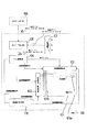
図1は、本発明の第1の実施の形態に係る液晶装置の一例である液晶モニターの模式図である。同図において、101は液晶素子である液晶パネルであり、この液晶パネル101は、薄膜トランジスタ等のスイッチング素子を各画素に配した、所謂アクティブマトリクス型液晶パネルであり、本実施形における液晶パネル101の表示領域は対角約13インチで、画素数はXGA(1024×768)である。
【0017】
また、105はパーソナルコンピュータなどの表示データ発生部であり、この表示データ発生部105からは、デジタル表示データ1(ID(5:0)、ID(15:10)、ID(25:20)、R(赤)、G(緑)、B(青)各色6ビット/ピクセル)と、制御信号(水平及び垂直同期信号、転送クロック、ブランキング信号など)とが液晶モニター100に送出される。
【0018】
また、107は色調調整手段である色調調整SWであり、この色調調整SW107は、デジタル・コードSWで構成され、R、G、B各色の色調をそれぞれ独立に調整する3ビットの色補正データ(RGB用にそれぞれCD(2:0)、CD(12:10)、CD(22:20))を出力する。なお、この各色3ビットの色補正データの最上位ビットは、所謂サインビットであり、補正データの極性(補正の方向)を表している。
【0019】
また、108は表示データ補正手段である表示データ補正回路であり、表示データ補正回路108は、表示データ発生部105からのデジタル表示データ1(6ビット/ピクセル)を、色補正データの残りの2ビット/ピクセルによって8ビット/ピクセルに拡張し、“表示データ2”としてパネル制御回路104に送出する。なお、この表示データ補正手段108の動作については後で詳しく述べる。
【0020】
また、104はパネル制御回路であり、このパネル制御回路104は、表示データ補正回路108によって補正された表示データ2を情報信号出力手段である情報電極駆動回路102に出力すると共に、表示データ発生部105からの制御信号に基づき、情報電極駆動回路102と走査電極駆動回路103への各種制御信号を生成する。
【0021】
また、106は駆動電圧発生回路であり、この駆動電圧発生回路106は、パネル制御回路104からの駆動電圧制御信号に基づき、所定の走査電極駆動電圧及び情報電極駆動電圧を発生し、それぞれ走査電極駆動回路103、情報電極駆動回路102に供給する。
【0022】
そして、走査電極駆動回路103及び情報電極駆動回路102は、駆動電圧発生回路106からの各駆動電圧、並びにパネル制御回路104からの各種制御信号及び表示データに基づき、それぞれ走査電極駆動波形、情報電極駆動波形を発生して液晶パネル101の走査電極101a及び情報電極101bに印加し、液晶パネル101を所定のフレーム周波数、駆動電圧で駆動する。
【0023】
なお、この情報電極駆動回路102は、オリジナルの入力データ“表示データ1”のビット数(6ビット)に、色補正データの拡張分(2ビット)を加えた、計8ビットの表示データ入力幅に対応するデータ入力部を有している。
【0024】
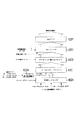
ここで、図2は、情報電極駆動回路102の構成を示すブロック図であり、この情報電極駆動回路102は、上記8ビットの表示データ入力幅に対応するデータ入力部としてパネル制御回路104からのシフト方向切替信号、イネーブル入出力信号及びクロック信号により作動する双方向ラッチセレクタ101A、8ビットの表示データ2を並び替えるデータ並び替え回路102B、データ並び替え回路102Bにより並び替えられた表示データ2を保持するデータレジスタ102C、このデータレジスタ102Cに保持された表示データ2をパネル制御回路104からのラッチ信号によりラッチするデータラッチ部102D、ラッチされたデータをD/A変換するD/Aコンバータ102E及び出力アンプ102Fを有している。
【0025】
なお、同図において、基準駆動電圧V0〜V8は、液晶パネル10lのγ特性カーブ上の主要9ポイントを決定するために、駆動電圧発生回路106から入力される電圧である。他方、各色8ビットの表示データはラッチ信号(LP)によってラッチされるが、情報信号駆動回路102にとっては入力される8ビットすべてが表示データであり、その表示データの中に前記補正データが含まれているか否かは関係ない。
【0026】
ここで、情報信号駆動回路102は、ラッチされた8ビットの表示データに基づき、図3に示すように上位3ビットによってγ補正電圧の一つの電圧範囲(Vn+1〜Vn)を選択し、下位5ビットはD/A変換によってVn+1〜Vn間をさらに均等に32分割することによって256通りの電圧を出力する。なお、入力される表示データと出力電圧の関係は図4に示すとおりである。
【0027】
一方、図5は、液晶パネル101への出力電圧と液晶の透過率の関係を示す図である。基本的に、既述した情報電極駆動回路102から出力される256通りの出力電圧に応じて、液晶パネルは256レベルの透過率を示すが、同図に示すように、一般的にこの特性はγ=1ではなく、やや複雑なS字状の特性をもつケースが多い。このため、液晶の透過率がリニアに変化するよう調整する目的で、前記基準駆動電圧V0〜V8を与えている。
【0028】
ところで、この出力電圧と液晶透過率との関係は、RGB各色ごとに微妙に異なっているため、本発明においては、色調調整SW107と表示データ拡張回路108を用いてRGB各色ごとにそれぞれ独立に色調調整を行うようにしている。
【0029】
ここで、色調調整SW107は、既述した通り一般的なデジタル・コードSWであり、調整位置に応じて各色3ビットの色補正データ(デジタル・コード)を出力するものである。なお、この色調調整SW107は、アナログトリマー(可変抵抗器)とA/D変換器の組み合わせによっても同様の機能を実現させることもできる。
【0030】
なお、図6は、本実施の形態における色補正データCD(x2:x0)(R:x=0、G:x=1、B:x=2)のコード表である。ここで、3ビットのうち、最上位ビットCIDx2は補正データの極性(補正の方向)を、残りの2ビットが補正量を表している。
【0031】
図7、図8は、本実施の形態における表示データ補正回路108の動作を説明する図である。
【0032】
ここで、既述したように表示データ補正回路108には、表示データ1(本実施の形態においてはRGB各色6ビット)と色補正データ(同3ビット)が入力される。そして、色補正データの最上位ビットが、“0”の場合は、図5の透過率特性のプラス方向に補正を行い、“1”であれば同じくマイナス方向に補正を行う。
【0033】
そして、図7がプラス補正を行う場合の処理フローである。ここで、プラス補正とは、入力される表示データに対する出力電圧(液晶駆動電圧)を補正なしの場合よりも上げ、液晶の透過率を上げる方向を指す。
【0034】
以下、そのフローを説明する。
【0035】
補正を行う場合、表示データ補正回路108は、まず色補正データの最上位ビットが“0”であることからプラス補正と判断し、表示データ発生部105から入力される図7の(a)に示す6ビットの表示データ1を、(b)に示すように2ビット分上位ビット側にシフトし、下位2ビットを“1”で埋める。
【0036】
その後、(c)に示すように下位2ビットに色調調整SW107からの色補正データの2ビットを減算処理し、その結果を(d)に示す8ビットの表示データ2として、パネル制御回路104に出力する。特に図示していないが、以上のような処理は、簡単なハードウェア「ビットシフト回路」と「加減算回路」で実現できる。
【0037】
一方、図8は、マイナス補正を行う場合の処理フローである。
【0038】
そして表示データ補正回路108は、補正を行う場合、まず色補正データの最上位ビットが“1”であることからマイナス補正と判断し、表示データ発生部105から入力される図8の(a)に示す6ビットの表示データ1を(b)に示すように2ビット分上位ビット側にシフトし、下位2ビットを“0”で埋める。
【0039】
その後、(c)に示すように下位2ビットに色調調整SW107からの色補正データの2ビットを加算処理し、その結果を(d)に示す8ビットの表示データ2として、パネル制御回路104に出力する。
【0040】
図9は、前記プラス補正時の表示データ補正回路108への入力データ(6ビット)と、色調整処理後の出力データ(8ビット)との関係を示す表である。
【0041】
一例として、入力データが“07H”の場合をみると、補正無しの出力電圧が「V7」、プラス補正最大(図6の+3)の出力電圧が「V7+(V8−V7)×3/32」である。すなわち、プラス方向に補正を最大に行った場合、補正なしに比べて「(V8−V7)×3/32」分だけ出力電圧が上がり、それに伴って液晶の透過率も変化(アップ)する。
【0042】
このように、本実施の形態においては、一つの入力データに対して、8ビット(256通り)の1LSB単位で、プラス方向、マイナス方向それぞれに3段階の色調調整が可能である。なお、図10は、このような補正を行った場合の液晶の透過率特性の変化を示す概念図である。
【0043】
そして、本発明においては、この補正処理をRGBそれぞれ独立(勿論、Rの表示データは、Rの色補正データで処理する)に行なっている。これにより、RGB各色ごとに微妙に異なっていた電圧−透過率特性を補正して一致させることが出来、全階調レベルにおいてカラーバランスを保った表示が可能になった。
【0044】
このように、色調調整SW107によりRGBの色調をそれぞれ独立に調整する色補正データを出力すると共に、表示データ補正回路108において色補正データによって表示データを補正することにより、MPU、ルックアップテーブル用RAMなどを用いることなく、安価かつ簡便な方法でRGB独立に色調調整を行うことができる。
【0045】
次に、本実施の形態の第2の実施の形態について説明する。
【0046】
本実施の形態においては、図1における色調調整SW107の色補正データのビット数をRGB各色5ビットに変更した。なお、色補正データの最上位ビットが、補正の方向を示すのは既述した第1の実施の形態と同様である。
【0047】
図11及び図12は、本実施の形態における表示データ補正回路108の処理フローを示すものである。
【0048】
ここで、この表示データ補正回路108の処理フローは、既述した第1の実施の形態と同様であるが、第1の実施の形態では、入力される表示データ1(6ビット)に色補正データ(2ビット)を拡張して、計8ビットにしたのに対し、本実施の形態では、補正処理後の表示データ幅が8ビットである点は同じであるが、演算処理としては表示データ1のLSB側2ビットに色補正データのMSB側2ビットが、オーバーラップする形の演算処理を行うようにしている。
【0049】
そして、このような演算処理を行うことにより、第1の実施の形態と同様の補正ピッチで、より広い範囲での補正が可能になった。
【0050】
なお、第1、第2の実施の形態と共に、6ビットの表示データに対して、補正データとしての拡張分を2ビットとし、計8ビットの表示データとして情報電極駆動回路102に出力する構成を採っているが、これは、あくまでも一例であり、思想的にはこのビット数に限定されるものではないことは言うまでもない。例えば、入力される表示データを8ビットとし、補正後10ビットの表示データとして情報電極駆動回路102に出力するようにしてもよい。
【0051】
【発明の効果】
以上説明したように本発明によれば、色調調整手段と、表示データ補正手段とを備え、表示データ補正手段において、色調調整手段により出力されるカラー画像の赤、緑及び青の色調をそれぞれ独立に調整する色補正データによりデジタル表示データを補正することができるので、より安価で簡便な方法で赤、緑及び青独立に色調調整を行うことができる。
【図面の簡単な説明】
【図1】本発明の第1の実施の形態に係る液晶装置の一例である液晶モニターの模式図。
【図2】上記液晶モニターの情報電極駆動回路の構成を示すブロック図。
【図3】上記液晶モニターに入力される表示データに応じて上記情報電極駆動回路が出力する電圧を示す図。
【図4】上記情報電極駆動回路の表示データと出力電圧との関係を示す図。
【図5】上記情報電極駆動回路の出力電圧と液晶パネルの透過率との関係の一例を示す図。
【図6】上記液晶モニターの色調調整SWから出力される色補正データの一例を示す図表。
【図7】上記液晶モニターの表示データ補正回路のプラス補正を行う場合の動作を説明する図。
【図8】上記表示データ補正回路のマイナス補正を行う場合の動作を説明する図。
【図9】上記表示データ補正回路の入力データと出力データとの関係の一例を示す図表。
【図10】上記表示データ補正回路の補正方向と液晶パネルの透過率との関係の一例を示す図。
【図11】本発明の第2の実施の形態に係る液晶モニターの表示データ補正回路におけるプラス補正を行う場合の動作を説明する図。
【図12】上記表示データ補正回路のマイナス補正を行う場合の動作を説明する図。
【図13】従来の色補正回路を含む液晶モニターの模式図。
【符号の説明】
100 液晶モニター
101 液晶パネル
102 情報電極駆動回路
103 走査電極駆動回路
104 パネル制御回路
105 表示データ発生部
107 色調調整SW
108 表示データ補正回路[0001]
BACKGROUND OF THE INVENTION
The present invention relates to a liquid crystal device including a liquid crystal element, and relates to color tone adjustment of a liquid crystal element that displays a color image based on digital display data.
[0002]
[Prior art]
In recent years, matrix type displays using liquid crystals (TFT, STN, FLC, AFLC, etc.) have made remarkable progress in terms of size and capacity.
[0003]
For example, screen sizes with a diagonal size of 10 to 14 inches for notebook PCs and 13 to 20 inches for desktop monitors have appeared, and in terms of display capacity, XGA (1024 × 768 pixels), SXGA (1280) × 1024) and even UXGA (1600 × l280) have been announced.
[0004]
As described above, liquid crystal displays that are comparable to CRTs in terms of screen size and display capacity will require further improvements in image quality as monitors, and are generally installed in CRT monitors and the like. More and more cases are equipped with image quality (ex. Color tone) adjustment functions.
[0005]
Incidentally, when image quality adjustment is performed on a liquid crystal monitor which is an example of a liquid crystal device, basically two methods are conceivable. One of them is a method of performing gain adjustment or the like in an analog manner at a video signal input unit in the case of a liquid crystal monitor having an analog input similar to a general CRT monitor.
[0006]
In the other case, in the case of a liquid crystal monitor having a so-called digital interface in which display data is inputted digitally, a simple MPU (microcontroller) 109 inside the
[0007]
Here, in general, there are many cases in which adjustment is performed digitally because of the stability of control and the matching with the device (liquid crystal) drive system, and even if the input of the liquid crystal monitor is analog, the input section In some cases, an A / D converter is provided to perform correction by digital processing similar to the latter.
[0008]
[Problems to be solved by the invention]
However, in such a conventional liquid crystal device, when image quality adjustment is performed, for example, when R (red), G (green), and B (blue) color tone adjustment is performed, the adjustment by the digital method has a degree of freedom of adjustment. On the other hand, there is a problem that the control becomes complicated and the cost of the components is increased because the MPU, the RAM for the lookup table, etc. are used.
[0009]
The present invention has been made to solve such problems, and an object of the present invention is to provide a liquid crystal device capable of adjusting the red, green, and blue color tone of a color image by an inexpensive and simple method. It is what.
[0010]
[Means for Solving the Problems]
The present invention includes a liquid crystal element for displaying a color image based on the digital display data, and the information signal output means for outputting the information signal based on the digital display data to the liquid crystal element, the color image of red, green and blue Color tone adjusting means for outputting color correction data of a plurality of bits for independently adjusting the color tone, and display data correction for correcting the digital display data with the color correction data from the color tone adjusting means and outputting it to the information signal output means And the color correction data includes a bit indicating an increase / decrease amount of the information signal value, and the display data correction unit is configured to correct the color correction on the lower bit side of the digital display data. The correction is performed by extending the number of bits indicating the increase / decrease amount of the data information signal value .
[0011]
Further, the present invention is characterized in that the display data correction means performs correction for increasing or decreasing the information signal value by the color correction data so as to adjust the red, green and blue color tones.
[0013]
The present invention also provides a liquid crystal element for displaying a color image based on digital display data, an information signal output means for outputting an information signal based on the digital display data to the liquid crystal element, and red, green and blue colors of the color image. Color tone adjustment means for outputting color correction data of a plurality of bits for independently adjusting the color tone of the image, and display data for correcting the digital display data with the color correction data from the color tone adjustment means and outputting it to the information signal output means The information signal output means has a data input unit having a number obtained by adding the number of bits of the color correction data to the number of extended bits of the color correction data. It is what.
[0014]
Further, as in the present invention, a plurality of bits of color correction data for independently adjusting the red, green and blue color tones of the color image are output by the color adjustment means, and the digital display data is converted by the display data correction means. After correction by the color correction data, an information signal based on the digital display data is output to an information signal output means for outputting to the liquid crystal element.
[0015]
DETAILED DESCRIPTION OF THE INVENTION
Hereinafter, embodiments of the invention will be described with reference to the drawings.
[0016]
FIG. 1 is a schematic diagram of a liquid crystal monitor which is an example of a liquid crystal device according to the first embodiment of the present invention. In the figure,
[0017]
[0018]
[0019]
[0020]
[0021]
[0022]
Then, the scan
[0023]
The information
[0024]
FIG. 2 is a block diagram showing the configuration of the information
[0025]
In the figure, reference drive voltages V0 to V8 are voltages input from the drive
[0026]
Here, the information
[0027]
On the other hand, FIG. 5 is a diagram showing the relationship between the output voltage to the
[0028]
Incidentally, since the relationship between the output voltage and the liquid crystal transmittance is slightly different for each RGB color, in the present invention, the color tone is independently adjusted for each RGB color by using the color
[0029]
Here, the color
[0030]
FIG. 6 is a code table of the color correction data CD (x2: x0) (R: x = 0, G: x = 1, B: x = 2) in the present embodiment. Here, among the 3 bits, the most significant bit CIDx2 represents the polarity (correction direction) of the correction data, and the remaining 2 bits represent the correction amount.
[0031]
7 and 8 are diagrams for explaining the operation of the display
[0032]
Here, as described above, the display
[0033]
FIG. 7 is a processing flow in the case where plus correction is performed. Here, plus correction refers to a direction in which the output voltage (liquid crystal drive voltage) for input display data is increased as compared to the case without correction, and the transmittance of the liquid crystal is increased.
[0034]
The flow will be described below.
[0035]
When correction is performed, the display
[0036]
After that, as shown in (c), 2 bits of the color correction data from the color
[0037]
On the other hand, FIG. 8 is a processing flow in the case where minus correction is performed.
[0038]
When the correction is performed, the display
[0039]
Thereafter, as shown in (c), 2 bits of the color correction data from the color
[0040]
FIG. 9 is a table showing the relationship between the input data (6 bits) to the display
[0041]
As an example, when the input data is “07H”, the output voltage without correction is “V7”, and the maximum output voltage (+3 in FIG. 6) is “V7 + (V8−V7) × 3/32”. It is. That is, when the correction is performed to the maximum in the plus direction, the output voltage is increased by “(V8−V7) × 3/32” compared to the case where the correction is not performed, and the transmittance of the liquid crystal is changed (up) accordingly.
[0042]
As described above, in this embodiment, it is possible to adjust the color tone in three stages in the plus direction and the minus direction in units of 1 LSB of 8 bits (256 types) for one input data. FIG. 10 is a conceptual diagram showing changes in the transmittance characteristics of the liquid crystal when such correction is performed.
[0043]
In the present invention, this correction processing is performed independently for each of RGB (of course, the R display data is processed by the R color correction data). As a result, the voltage-transmittance characteristics that have been slightly different for each of the RGB colors can be corrected and matched, and display with a color balance maintained at all gradation levels is possible.
[0044]
In this way, the color correction data for independently adjusting the RGB color tones are output by the color
[0045]
Next, a second embodiment of the present embodiment will be described.
[0046]
In the present embodiment, the number of bits of color correction data of the color
[0047]
11 and 12 show a processing flow of the display
[0048]
Here, the processing flow of the display
[0049]
By performing such arithmetic processing, it is possible to perform correction in a wider range at the same correction pitch as in the first embodiment.
[0050]
Along with the first and second embodiments, a configuration in which 6-bit display data is extended to 2 bits as correction data and output to the information
[0051]
【The invention's effect】
As described above, according to the present invention, the color tone adjusting means and the display data correcting means are provided, and in the display data correcting means, the red, green, and blue color tones of the color image output by the color tone adjusting means are independent of each other. Since the digital display data can be corrected by the color correction data to be adjusted in the following manner, the color tone can be adjusted independently for red, green and blue by a cheaper and simple method.
[Brief description of the drawings]
FIG. 1 is a schematic diagram of a liquid crystal monitor which is an example of a liquid crystal device according to a first embodiment of the invention.
FIG. 2 is a block diagram showing a configuration of an information electrode driving circuit of the liquid crystal monitor.
FIG. 3 is a diagram illustrating a voltage output from the information electrode driving circuit in accordance with display data input to the liquid crystal monitor.
FIG. 4 is a diagram showing a relationship between display data and output voltage of the information electrode driving circuit.
FIG. 5 is a diagram showing an example of the relationship between the output voltage of the information electrode driving circuit and the transmittance of the liquid crystal panel.
FIG. 6 is a table showing an example of color correction data output from a color tone adjustment SW of the liquid crystal monitor.
FIG. 7 is a diagram for explaining an operation when performing positive correction of a display data correction circuit of the liquid crystal monitor.
FIG. 8 is a diagram for explaining an operation when the display data correction circuit performs a negative correction.
FIG. 9 is a table showing an example of a relationship between input data and output data of the display data correction circuit.
FIG. 10 is a diagram showing an example of the relationship between the correction direction of the display data correction circuit and the transmittance of the liquid crystal panel.
FIG. 11 is a diagram for explaining an operation when performing positive correction in a display data correction circuit of a liquid crystal monitor according to a second embodiment of the present invention.
FIG. 12 is a diagram for explaining an operation when the display data correction circuit performs a negative correction.
FIG. 13 is a schematic diagram of a liquid crystal monitor including a conventional color correction circuit.
[Explanation of symbols]
DESCRIPTION OF
108 Display data correction circuit
Claims (3)
前記色補正データは、情報信号値の増減量を示すビットを有し、前記表示データ補正手段は、前記デジタル表示データの下位ビット側に前記色補正データの情報信号値の増減量を示すビット数を拡張することにより前記補正を行うことを特徴とする液晶装置。Each independently a liquid crystal element for displaying a color image based on the digital display data, and the information signal output means for outputting the information signal based on the digital display data to the liquid crystal element, the red of the color image, green and blue shades A color tone adjusting unit that outputs a plurality of bits of color correction data to be adjusted, and a display data correcting unit that corrects the digital display data with color correction data from the color tone adjusting unit and outputs the corrected data to the information signal output unit. A liquid crystal device comprising:
The color correction data has a bit indicating an increase / decrease amount of the information signal value, and the display data correction means has a bit number indicating an increase / decrease amount of the information signal value of the color correction data on the lower bit side of the digital display data. The liquid crystal device is characterized in that the correction is performed by expanding the function .
前記情報信号出力手段は、前記デジタル表示データのビット数に前記色補正データの拡張ビット数分を加えた数のデータ入力部を有することを特徴とする液晶装置。 A liquid crystal element that displays a color image based on digital display data, an information signal output means that outputs an information signal based on the digital display data to the liquid crystal element, and the red, green, and blue tones of the color image are independent of each other A color tone adjusting unit that outputs a plurality of bits of color correction data to be adjusted, and a display data correcting unit that corrects the digital display data with color correction data from the color tone adjusting unit and outputs the corrected data to the information signal output unit. A liquid crystal device comprising:
It said information signal output means, a liquid crystal device you further comprising a data input unit number plus number of extension bits of the color correction data to the number of bits of the digital display data.
Priority Applications (1)
| Application Number | Priority Date | Filing Date | Title |
|---|---|---|---|
| JP17937198A JP3962484B2 (en) | 1998-06-25 | 1998-06-25 | Liquid crystal device |
Applications Claiming Priority (1)
| Application Number | Priority Date | Filing Date | Title |
|---|---|---|---|
| JP17937198A JP3962484B2 (en) | 1998-06-25 | 1998-06-25 | Liquid crystal device |
Publications (2)
| Publication Number | Publication Date |
|---|---|
| JP2000010532A JP2000010532A (en) | 2000-01-14 |
| JP3962484B2 true JP3962484B2 (en) | 2007-08-22 |
Family
ID=16064692
Family Applications (1)
| Application Number | Title | Priority Date | Filing Date |
|---|---|---|---|
| JP17937198A Expired - Fee Related JP3962484B2 (en) | 1998-06-25 | 1998-06-25 | Liquid crystal device |
Country Status (1)
| Country | Link |
|---|---|
| JP (1) | JP3962484B2 (en) |
Families Citing this family (4)
| Publication number | Priority date | Publication date | Assignee | Title |
|---|---|---|---|---|
| JP3512710B2 (en) | 2000-05-30 | 2004-03-31 | Nec液晶テクノロジー株式会社 | Liquid crystal display |
| JP4201070B2 (en) * | 2000-06-28 | 2008-12-24 | エルジー ディスプレイ カンパニー リミテッド | Apparatus and method for correcting gamma voltage of liquid crystal display device |
| US7030846B2 (en) | 2001-07-10 | 2006-04-18 | Samsung Electronics Co., Ltd. | Color correction liquid crystal display and method of driving same |
| WO2005057276A1 (en) | 2003-12-11 | 2005-06-23 | Toshiba Matsushita Display Technology Co., Ltd. | Liquid crystal display device |
-
1998
- 1998-06-25 JP JP17937198A patent/JP3962484B2/en not_active Expired - Fee Related
Also Published As
| Publication number | Publication date |
|---|---|
| JP2000010532A (en) | 2000-01-14 |
Similar Documents
| Publication | Publication Date | Title |
|---|---|---|
| JP4986334B2 (en) | Liquid crystal display device and driving method thereof | |
| US7176867B2 (en) | Liquid crystal display and driving method thereof | |
| JP3495960B2 (en) | Gray scale display reference voltage generating circuit and liquid crystal driving device using the same | |
| JP4807924B2 (en) | Liquid crystal display device and driving device thereof | |
| US7126572B2 (en) | Image display method and image display device | |
| JP5035973B2 (en) | Liquid crystal display device and control driver for the liquid crystal display device | |
| US7898517B2 (en) | Display device, data driver IC, and timing controller | |
| JP2003280596A (en) | Display driving apparatus and display apparatus using the same | |
| JP2003308048A (en) | Liquid crystal display device | |
| JP2001119717A (en) | White point adjustment method, color image processing method, white point adjustment device and liquid crystal display device | |
| WO2006068224A1 (en) | Display device and drive method thereof | |
| JP2006039538A (en) | Driving circuit of liquid crystal display device and method for driving same | |
| JP2006171761A (en) | Display device and driving method thereof | |
| US6909435B2 (en) | Reduction of gamma correction contouring in liquid crystal on silicon (LCOS) displays | |
| JP3962484B2 (en) | Liquid crystal device | |
| CN113808550A (en) | Device applicable to brightness enhancement in display module | |
| JP2954329B2 (en) | Multi-tone image display device | |
| JP4497793B2 (en) | Method and apparatus for driving liquid crystal display device | |
| JP2000194325A (en) | Liquid crystal display device and signal processing method therefor | |
| JP2008111925A (en) | Liquid crystal display apparatus | |
| JP2001282190A (en) | Liquid crystal display device, medium, and information assembly | |
| JP2004120366A (en) | Apparatus and method for image processing | |
| JP2005258381A (en) | Color management structure for panel display and its method | |
| KR100806909B1 (en) | device for driving liquid crystal device | |
| KR20070080100A (en) | Frame date correction circuit and liquid crystal display comprising the same |
Legal Events
| Date | Code | Title | Description |
|---|---|---|---|
| A621 | Written request for application examination |
Free format text: JAPANESE INTERMEDIATE CODE: A621 Effective date: 20041214 |
|
| A977 | Report on retrieval |
Free format text: JAPANESE INTERMEDIATE CODE: A971007 Effective date: 20070213 |
|
| A131 | Notification of reasons for refusal |
Free format text: JAPANESE INTERMEDIATE CODE: A131 Effective date: 20070220 |
|
| A521 | Written amendment |
Free format text: JAPANESE INTERMEDIATE CODE: A523 Effective date: 20070419 |
|
| TRDD | Decision of grant or rejection written | ||
| A01 | Written decision to grant a patent or to grant a registration (utility model) |
Free format text: JAPANESE INTERMEDIATE CODE: A01 Effective date: 20070515 |
|
| A61 | First payment of annual fees (during grant procedure) |
Free format text: JAPANESE INTERMEDIATE CODE: A61 Effective date: 20070521 |
|
| R150 | Certificate of patent or registration of utility model |
Free format text: JAPANESE INTERMEDIATE CODE: R150 |
|
| FPAY | Renewal fee payment (event date is renewal date of database) |
Free format text: PAYMENT UNTIL: 20100525 Year of fee payment: 3 |
|
| FPAY | Renewal fee payment (event date is renewal date of database) |
Free format text: PAYMENT UNTIL: 20110525 Year of fee payment: 4 |
|
| FPAY | Renewal fee payment (event date is renewal date of database) |
Free format text: PAYMENT UNTIL: 20120525 Year of fee payment: 5 |
|
| FPAY | Renewal fee payment (event date is renewal date of database) |
Free format text: PAYMENT UNTIL: 20120525 Year of fee payment: 5 |
|
| FPAY | Renewal fee payment (event date is renewal date of database) |
Free format text: PAYMENT UNTIL: 20130525 Year of fee payment: 6 |
|
| FPAY | Renewal fee payment (event date is renewal date of database) |
Free format text: PAYMENT UNTIL: 20140525 Year of fee payment: 7 |
|
| LAPS | Cancellation because of no payment of annual fees |