JP3962296B2 - Ferroelectric memory device and manufacturing method thereof - Google Patents
Ferroelectric memory device and manufacturing method thereof Download PDFInfo
- Publication number
- JP3962296B2 JP3962296B2 JP2002224451A JP2002224451A JP3962296B2 JP 3962296 B2 JP3962296 B2 JP 3962296B2 JP 2002224451 A JP2002224451 A JP 2002224451A JP 2002224451 A JP2002224451 A JP 2002224451A JP 3962296 B2 JP3962296 B2 JP 3962296B2
- Authority
- JP
- Japan
- Prior art keywords
- film
- hydrogen barrier
- barrier film
- ferroelectric
- line direction
- Prior art date
- Legal status (The legal status is an assumption and is not a legal conclusion. Google has not performed a legal analysis and makes no representation as to the accuracy of the status listed.)
- Expired - Lifetime
Links
Images


Description
【0001】
【発明の属する技術分野】
本発明は、半導体基板上に順次形成された、下部電極、強誘電体膜よりなる容量絶縁膜及び上部電極を有し、ワード線方向及びビット線方向にマトリックス状に配置された複数の強誘電体キャパシタを備えた強誘電体メモリ装置及びその製造方法に関する。
【0002】
【従来の技術】
近年、半導体メモリ装置としては、例えばSrBi2Ta2O9 (以下、SBTと記す)又はPb(Zr,Ti)O3 (以下、PZTと記す)等のヒステリシス特性を有する強誘電体材料膜よりなる容量絶縁膜を有する不揮発性の強誘電体メモリ装置が開発されている。このような強誘電体メモリ装置に用いられるSBT及びPZT等の強誘電体材料は強誘電体酸化物である。
【0003】
このため、複数の強誘電体キャパシタの上に層間絶縁膜を介してアルミ配線を形成した後に、半導体基板に形成されているMOSトランジスタの特性を確保するために行なわれる水素を含む雰囲気中での熱処理、又は半導体メモリ装置の微細化に伴うアスペクト比が高いコンタクトホールにタングステン膜を埋め込むために行なわれるCVD法において、強誘電体酸化物が還元性雰囲気、特に水素雰囲気に曝されると、強誘電体酸化物は還元される。このため、強誘電体酸化物の結晶組成が崩れてしまうので、容量絶縁膜の絶縁特性又は強誘電体酸化物の特性が大きく劣化してしまう。
【0004】
そこで、強誘電体キャパシタを形成した後に、該強誘電体キャパシタに対して水素雰囲気中での熱処理を施しても、強誘電体キャパシタの容量絶縁膜が水素に曝されて還元されることがないように、容量絶縁膜への水素の侵入を防止する水素バリア膜を強誘電体キャパシタを覆うように形成する。
【0005】
ところが、強誘電体キャパシタと該強誘電体キャパシタの上に形成される層間絶縁膜との間に水素バリア膜を設ける場合、水平方向からの水素の侵入を遮断するためには、水素バリア膜の面積を強誘電体キャパシタの面積よりも少なくとも数μm以上大きくする必要がある。また、水素バリア膜は層間絶縁膜に埋め込まれたコンタクトプラグの上にも形成されるため、コンタクトプラグをCVD法により形成されるタングステン膜により形成する場合には、水素バリア膜が有する容量絶縁膜への水素の侵入を防止する効果は低減する。
【0006】
特に、近年、強誘電体メモリ装置の微細化に伴って強誘電体キャパシタの面積の縮小化(1μm2 以下)が図られているが、前述の理由により、水素バリア膜により強誘電体キャパシタを覆うだけでは、容量絶縁膜への水素の侵入を確実に防止することができない。
【0007】
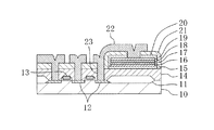
そこで、特開平11−135736号公報においては、図6に示すような構造を有する強誘電体メモリ装置が提案されている。
【0008】
以下、従来例として、図6に示す強誘電体メモリ装置について説明する。
【0009】
シリコン基板10の表面部には、素子分離領域11が形成されていると共にソース又はドレインとなる不純物拡散層12が形成されている。シリコン基板10の上における不純物拡散領域12同士の間には、ゲート絶縁膜を介してゲート電極13が形成されており、これらゲート電極13及び不純物拡散層12により電界効果型トランジスタが構成されている。
【0010】
電界効果型トランジスタ及び素子分離領域11の上には第1の層間絶縁膜14が形成されており、該第1の層間絶縁膜14の上における素子分離領域11の上方には第1の絶縁性水素バリア膜15が形成されている。第1の絶縁性水素バリア膜15の上には、下部電極16、強誘電体膜よりなる容量絶縁膜17及び上部電極18から構成される強誘電体キャパシタが形成されている。上部電極18の上には導電性水素バリア膜19が形成され、該導電性水素バリア膜19の上面、並びに下部電極16、容量絶縁膜17及び上部電極18の側面を覆うように第2の絶縁性水素バリア膜20が形成されており、強誘電体キャパシタは、第1の絶縁性水素バリア膜15、導電性水素バリア膜19及び第2の絶縁性水素バリア膜20により完全に覆われている。
【0011】
第1の層間絶縁膜14及び第2の絶縁性水素バリア膜20の上には第2の層間絶縁膜21が形成されている。第2の層間絶縁膜21の上には金属配線22が形成されており、該金属配線22は、第1の層間絶縁膜14及び第2の層間絶縁膜21に埋め込まれたコンタクトプラグ23と接続している。
【0012】
【発明が解決しようとする課題】
前述のように、強誘電体キャパシタは、第1の絶縁性水素バリア膜15、導電性水素バリア膜19及び第2の絶縁性水素バリア膜20により完全に覆われているため、容量絶縁膜17に水素が侵入する事態は防止できる。
【0013】
ところが、前記従来の強誘電体メモリ装置においては、第2の絶縁性水素バリア膜20をパターニングする際のマスクずれにより、第2の絶縁性水素バリア膜20の側部が消滅してしまったり、膜厚が薄くなってしまったりする事態が発生する。
【0014】
そこで、第2の絶縁性水素バリア膜20の膜厚を厚くすると共に、第2の絶縁性水素バリア膜20をパターニングするためのマスクのマージンを大きくする必要がある。
【0015】
このため、強誘電体キャパシタ同士の間隔を大きくする必要があるので、強誘電体メモリ装置の微細化が困難になるという問題がある。
【0016】
前記に鑑み、本発明は、強誘電体キャパシタの容量絶縁膜に水素が侵入する事態の確実な防止と、強誘電体メモリ装置の微細化との両立を図ることを目的とする。
【0017】
【課題を解決するための手段】
前記の目的を達成するため、本発明の請求項1に係る強誘電体メモリ装置は、半導体基板上の層間絶縁膜の上に順次形成された下部電極、強誘電体膜よりなる容量絶縁膜及び上部電極を有し、ワード線方向及びビット線方向に配置された複数の強誘電体キャパシタを備えた強誘電体メモリ装置であって、
複数の前記上部電極を覆うように設けられ、Si3N4膜、SiON膜、Al2O3膜、TiO2膜、TiN膜若しくはTiとAlとの合金膜、又はTiとAlとの合金の酸化物膜、窒化物膜若しくは酸窒化物膜よりなる第2の水素バリア膜を備え、
前記第2の水素バリア膜は、ワード線方向及びビット線方向のうちの一方向に並ぶ前記複数の強誘電体キャパシタよりなるキャパシタ列毎に分離して形成され、
前記複数の強誘電体キャパシタのうち、前記一方向に並ぶ複数の強誘電体キャパシタの前記下部電極同士の間に埋め込まれ、上面が前記下部電極の上面とほぼ面一に形成された絶縁性の第1の水素バリア膜と、
前記層間絶縁膜に形成されているコンタクトプラグと前記下部電極との間に形成されている導電性水素バリア膜とをさらに備え、
前記第2の水素バリア膜の周縁部は、前記第1の水素バリア膜の上面と接続され、
前記一方向に並ぶ前記複数の強誘電体キャパシタよりなるキャパシタ列は、前記第2の水素バリア膜、前記第1の水素バリア膜及び前記導電性水素バリア膜によって完全に覆われている。
【0018】
本発明の請求項1に係る強誘電体メモリ装置によると、上部電極を覆うように第2の水素バリア膜が形成されているため、強誘電体キャパシタを形成した後において水素雰囲気中での熱処理が施された場合、強誘電体キャパシタの容量絶縁膜に対して上方から侵入する水素を防止できるので、容量絶縁膜を構成する強誘電体膜の還元を防止することができる。
また、ワード線方向及びビット線方向のうちの一方向に並ぶ複数の強誘電体キャパシタの下部電極同士の間に第1の絶縁性水素バリア膜が埋め込まれているため、第1の絶縁性水素バリア膜における、一方向に並ぶ複数の強誘電体キャパシタの下部電極同士の間の領域ではパターニングする必要はない。このため、パターニングを行なうためのマスクの位置ずれを考慮して、下部電極同士の間に寸法マージンを確保する必要がないので、強誘電体キャパシタ同士の間隔を狭くして、メモリセルアレイひいては強誘電体メモリ装置の面積を低減することができる。
【0019】
本発明の請求項2に係る強誘電体メモリ装置は、半導体基板上の層間絶縁膜の上に順次形成された下部電極、強誘電体膜よりなる容量絶縁膜及び上部電極を有し、ワード線方向及びビット線方向に配置された複数の強誘電体キャパシタを備えた強誘電体メモリ装置であって、
複数の前記上部電極を覆うように設けられ、Si3N4膜、SiON膜、Al2O3膜、TiO2膜、TiN膜若しくはTiとAlとの合金膜、又はTiとAlとの合金の酸化物膜、窒化物膜若しくは酸窒化物膜よりなる第2の水素バリア膜を備え、
前記第2の水素バリア膜は、ワード線方向及びビット線方向のうちの一方向に並ぶ前記複数の強誘電体キャパシタよりなるキャパシタ列のうち、ワード線方向及びビット線方向のうちの他方向に隣り合う一対のキャパシタ列を覆うように形成され、
前記複数の強誘電体キャパシタのうち、前記一対のキャパシタ列の前記複数の強誘電体キャパシタの前記下部電極同士の間に埋め込まれ、上面が前記下部電極の上面とほぼ面一に形成された絶縁性の第1の水素バリア膜と、
前記層間絶縁膜に形成されているコンタクトプラグと前記下部電極との間に形成されている導電性水素バリア膜とをさらに備え、
前記第2の水素バリア膜の周縁部は、前記第1の水素バリア膜の上面と接続され、
前記複数の強誘電体キャパシタよりなる前記一対のキャパシタ列は、前記第2の水素バリア膜、前記第1の水素バリア膜及び前記導電性水素バリア膜によって完全に覆われている。
【0021】
本発明の請求項2に係る強誘電体メモリ装置によると、第2の水素バリア膜における、一方向に並ぶ複数の強誘電体キャパシタよりなる一対のキャパシタ列同士の間において寸法マージンを確保する必要がないので、一対のキャパシタ列同士の間隔を狭くして、メモリセルアレイひいては強誘電体メモリ装置の面積を低減することができる。また、強誘電体メモリ装置の選択用トランジスタの近傍に、水素バリア膜が形成されていない領域が存在するため、金属配線を形成した後にトランジスタの特性を回復するために行なう水素雰囲気中での熱処理において、水素が選択トランジスタに拡散するための経路を確保することができる。
【0022】
本発明の請求項3に係る強誘電体メモリ装置は、請求項1または請求項2記載の強誘電体メモリ装置において、前記上部電極は、前記一方向に並ぶ前記複数の強誘電体キャパシタに共通に形成されていることを特徴とする。
【0028】
本発明の請求項4に係る強誘電体メモリ装置によると、請求項3に記載の強誘電体メモリ装置において、前記共通の上部電極と前記第2の水素バリア膜との間に形成され、前記共通の上部電極の周縁部に形成される段差を緩和する段差緩和膜が形成されていることが好ましい。
【0029】
このようにすると、パターニングされた上部電極の周端部に形成される角張った段差が緩和されるため、第2の水素バリア膜の上部電極の周端部におけるカバレッジを向上させることができる。
【0030】
本発明の請求項5に係る強誘電体メモリ装置によると、請求項1または請求項2に記載の強誘電体メモリ装置において、前記第1の水素バリア膜としては、Si3N4膜、SiON膜、Al2O3膜、TiO2 膜、又はTiとAlとの合金の酸化物膜若しくは酸窒化物を用いることができる。
【0032】
本発明の請求項6に係る強誘電体メモリ装置によると、請求項1または2に記載の強誘電体メモリ装置において、前記導電性水素バリア膜としては、TiとAlとの合金膜、TiとAlとの合金の窒化物膜若しくは酸窒化物膜、又はTiN膜を用いることができる。
【0033】
本発明の請求項7に係る強誘電体メモリ装置の製造方法は、半導体基板上の層間絶縁膜の上に順次形成された下部電極、強誘電体膜よりなる容量絶縁膜及び上部電極を有し、ワード線方向及びビット線方向に配置された複数の強誘電体キャパシタを備えた強誘電体メモリ装置の製造方法であって、
前記層間絶縁膜に形成されているコンタクトプラグの上に導電性水素バリア膜を形成する工程と、
前記導電性水素バリア膜の上に、前記複数の強誘電体キャパシタの下部電極を形成する工程と、
前記層間絶縁膜及び前記下部電極の上に絶縁性の第1の水素バリア膜を堆積した後、該第1の水素バリア膜を平坦化して、前記複数の強誘電体キャパシタのうち、ワード線方向及びビット線方向のうちの一方向に並ぶ前記複数の強誘電体キャパシタの前記下部電極同士の間に前記第1の水素バリア膜を埋め込んで、前記下部電極の上面と前記第1の水素バリア膜の上面をほぼ面一に形成する工程と、
前記下部電極上に容量絶縁膜を形成する工程と、
前記容量絶縁膜の上に上部電極を形成する工程と、
Si3N4膜、SiON膜、Al2O3膜、TiO2膜、TiN膜若しくはTiとAlとの合金膜、又はTiとAlとの合金の酸化物膜、窒化物膜若しくは酸窒化物膜よりなる第2の水素バリア膜を、複数の前記上部電極を覆い、かつ、ワード線方向及びビット線方向のうちの前記一方向に並ぶ前記複数の強誘電体キャパシタよりなるキャパシタ列毎に分離して形成するとともに、周縁部は前記第1の水素バリア膜の上面と接続するように形成する工程とを備え、
前記一方向に並ぶ前記複数の強誘電体キャパシタよりなるキャパシタ列は、前記第2の水素バリア膜、前記第1の水素バリア膜及び前記導電性水素バリア膜によって完全に覆われている。
【0034】
本発明の請求項7に係る強誘電体メモリ装置の製造方法によると、上部電極を覆うように第2の水素バリア膜を形成する工程を備えているため、強誘電体キャパシタを形成した後において水素雰囲気中での熱処理が施された場合、強誘電体キャパシタの容量絶縁膜に対して上方から侵入する水素を防止できるので、容量絶縁膜を構成する強誘電体膜の還元を防止することができる。
また、一方向に並ぶ複数の強誘電体キャパシタの下部電極同士の間に第1の絶縁性水素バリア膜が埋め込まれているため、第1の絶縁性水素バリア膜における、一方向に並ぶ複数の強誘電体キャパシタの下部電極同士の間の領域ではパターニングする必要はない。このため、パターニングを行なうためのマスクの位置ずれを考慮して、下部電極同士の間に寸法マージンを確保する必要がないので、強誘電体キャパシタ同士の間隔を狭くして、メモリセルアレイひいては強誘電体メモリ装置の面積を低減することができる。
【0036】
本発明の請求項8に係る強誘電体メモリ装置の製造方法は、半導体基板上の層間絶縁膜の上に順次形成された下部電極、強誘電体膜よりなる容量絶縁膜及び上部電極を有し、ワード線方向及びビット線方向に配置された複数の強誘電体キャパシタを備えた強誘電体メモリ装置の製造方法であって、
前記層間絶縁膜に形成されているコンタクトプラグの上に導電性水素バリア膜を形成する工程と、
前記導電性水素バリア膜の上に、前記複数の強誘電体キャパシタの下部電極を形成する工程と、
前記層間絶縁膜及び前記下部電極の上に絶縁性の第1の水素バリア膜を堆積した後、該第1の水素バリア膜を平坦化して、前記複数の強誘電体キャパシタのうち、ワード線方向及びビット線方向のうちの一方向に並ぶ前記複数の強誘電体キャパシタよりなるキャパシタ列のうち、ワード線方向及びビット線方向のうちの他方向に隣り合う一対のキャパシタ列の前記複数の強誘電体キャパシタの前記下部電極同士の間に前記第1の水素バリア膜を埋め込んで、前記下部電極の上面と前記第1の水素バリア膜の上面をほぼ面一に形成する工程と、
前記下部電極上に容量絶縁膜を形成する工程と、
前記容量絶縁膜の上に上部電極を形成する工程と、
Si3N4膜、SiON膜、Al2O3膜、TiO2膜、TiN膜若しくはTiとAlとの合金膜、又はTiとAlとの合金の酸化物膜、窒化物膜若しくは酸窒化物膜よりなる第2の水素バリア膜を、複数の前記上部電極を覆い、かつ、ワード線方向及びビット線方向のうちの前記一方向に並ぶ前記複数の強誘電体キャパシタよりなるキャパシタ列のうち、ワード線方向及びビット線方向のうちの他方向に隣り合う一対のキャパシタ列を覆うように形成するとともに、周縁部は前記第1の水素バリア膜の上面と接続するように形成する工程とを備え、
前記複数の強誘電体キャパシタよりなる前記一対のキャパシタ列は、前記第2の水素バリア膜、前記第1の水素バリア膜及び前記導電性水素バリア膜によって完全に覆われている。
【0037】
このようにすると、第2の水素バリア膜における、一方向に並ぶ複数の強誘電体キャパシタよりなる一対のキャパシタ列同士の間において寸法マージンを確保する必要がないので、一対のキャパシタ列同士の間隔を狭くして、メモリセルアレイひいては強誘電体メモリ装置の面積を低減することができる。また、強誘電体メモリ装置の選択用トランジスタの近傍に、水素バリア膜が形成されていない領域が存在するため、金属配線を形成した後にトランジスタの特性を回復するために行なう水素雰囲気中での熱処理において、水素が選択トランジスタに拡散するための経路を確保することができる。
【0044】
本発明の請求項9に係る強誘電体メモリ装置の製造方法は、共通の上部電極を形成する工程と第2の水素バリア膜を形成する工程との間に、共通の上部電極と第1の水素バリア膜との間に介在し、共通の上部電極の周縁部に形成される段差を緩和する段差緩和膜を形成する工程をさらに備えていることが好ましい。
【0045】
このようにすると、パターニングされた上部電極の周端部に形成される角張った段差が緩和されるので、第2の水素バリア膜の上部電極の周端部におけるカバレッジを向上させることができる。
【0046】
本発明の請求項10に係る強誘電体メモリ装置の製造方法において、前記第1の水素バリア膜としては、Si3N4膜、SiON膜、Al2O3膜、TiO2 膜、又はTiとAlとの合金の酸化物膜若しくは酸窒化物を用いることができる。
【0048】
本発明の請求項11に係る強誘電体メモリ装置の製造方法において、前記導電性水素バリア膜は、TiとAlとの合金膜、TiとAlとの合金の窒化物膜若しくは酸窒化物膜、又はTiN膜を用いることができる。
【0049】
【発明の実施の形態】
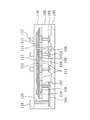
以下、本発明の一実施形態に係る強誘電体メモリ装置の構造について、図1及び図2を参照しながら説明する。
【0050】
本発明の一実施形態に係る強誘電体メモリ装置は、ワード線方向及びビット線方向にマトリックス状に配置された複数のメモリセルよりなるメモリセルアレイを備えている。図1は強誘電体メモリ装置におけるワード線に平行な面の断面構造を示し、図2は強誘電体メモリ装置におけるビット線に平行な面の断面構造を示している。
【0051】
図1及び図2に示すように、シリコンよりなる半導体基板100の表面部には素子分離領域101が形成されており、半導体基板100上における素子分離領域101により囲まれた領域には、ゲート絶縁膜を介してゲート電極102が形成されている。半導体基板100の表面部におけるゲート電極102の両側には、ソース又はドレインとなる第1の高濃度不純物拡散層103A、103Bが形成されており、ゲート電極102及び第1の不純物拡散層103A、103Bによって電界効果型トランジスタが構成されている。尚、半導体基板100の表面部におけるメモリセルアレイの周縁部には、第2の高濃度不純物拡散層104が形成されている。
【0052】
半導体基板100の上には、電界効果型トランジスタを覆うように第1の層間絶縁膜105が形成されている。第1の層間絶縁膜105には、第1のコンタクトプラグ106及び第2のコンタクトプラグ107がそれぞれ埋め込まれており、第1のコンタクトプラグ106の下端は第1の高濃度不純物拡散層103Aに接続されていると共に、第2のコンタクトプラグ107の下端は第2の高濃度不純物拡散層104に接続されている。
【0053】
第1の層間絶縁膜105の上には、第1のコンタクトプラグ106の上端又は第2のコンタクトプラグ107の上端と接続するように導電性水素バリア膜108がそれぞれ形成されており、第1のコンタクトプラグ106の上に位置する導電性水素バリア膜108の上には下部電極109が形成されていると共に、第2のコンタクトプラグ107の上に位置する導電性水素バリア膜108の上には上部電極中継部110が形成されている。
【0054】
第1の層間絶縁膜105の上には、下部電極109及び上部電極中継部110を取り囲むように絶縁性の第1の水素バリア膜111が形成されており、下部電極109の上面、上部電極中継部110の上面及び絶縁性の第1の水素バリア膜111の上面は、ほぼ面一に形成されている。本実施形態においては、図1に示すように、ワード線方向に並ぶ下部電極109同士の間には絶縁性の第1の水素バリア膜111が隙間なく埋め込まれているが、図2に示すように、ビット線方向に並ぶ下部電極109同士の間に形成されている絶縁性の第1の水素バリア膜111同士の間には隙間が形成されている。
【0055】
ワード線方向に並ぶ下部電極109及び絶縁性の第1の水素バリア膜111の上には、強誘電体膜よりなり、ワード線方向に並ぶ強誘電体キャパシタに共通の容量絶縁膜112が形成されており、該容量絶縁膜112における上部電極中継部110の上には開口部が形成されている。容量絶縁膜112の上には、ワード線方向に並ぶ強誘電体キャパシタに共通の上部電極113が形成されており、該上部電極113は容量絶縁膜の開口部を介して上部電極中継部110と接続している。以上説明した、下部電極109、容量絶縁膜112及び上部電極113によって強誘電体キャパシタが構成されていると共に、容量絶縁膜112及び上部電極113は、ワード線方向に並ぶ複数の強誘電体キャパシタよりなるキャパシタ列に共通に設けられている。
【0056】
上部電極113の上には、段差緩和膜114を介して第2の水素バリア膜115が形成されており、該第2の水素バリア膜115の周縁部は絶縁性の第1の水素バリア膜111の上面と接続している。これによって、ワード線方向に並ぶ複数の強誘電体キャパシタよりなるキャパシタ列は、導電性水素バリア膜108、絶縁性の第1の水素バリア膜111及び第2の水素バリア膜115によって完全に覆われている。
【0057】
第1の層間絶縁膜105の上には、第2の水素バリア膜115を覆うように第2の層間絶縁膜116が形成され、該第2の層間絶縁膜116の上には第1の金属配線117及び第2の金属配線118が形成されている。第1の金属配線117と第1の高濃度不純物拡散層103Bとは、第1の層間絶縁膜105及び第2の層間絶縁膜116に埋め込まれた第3のコンタクトプラグ119によって接続されていると共に、第2の金属配線118と第2の高濃度不純物拡散層104とは第1の層間絶縁膜105及び第2の層間絶縁膜116に埋め込まれた第4のコンタクトプラグ120によって接続されている。
【0058】
本発明の一実施形態に係る強誘電体メモリ装置によると、ワード線方向に並ぶ複数の強誘電体キャパシタの下部電極109同士の間には絶縁性の第1の素バリア膜111が埋め込まれている構造であって、絶縁性の第1の水素バリア膜111における、ワード線方向に並ぶ複数の強誘電体キャパシタの下部電極109同士の間の領域ではパターニングする必要はない。このため、パターニングを行なうためのマスクの位置ずれを考慮して、下部電極109同士の間に寸法マージンを確保する必要がないので、強誘電体キャパシタ同士の間隔を狭くしてメモリセルアレイの面積を低減することができる。
【0059】
また、ワード線方向に並ぶ複数の強誘電体キャパシタよりなるキャパシタ列は、導電性水素バリア膜108、絶縁性の第1の水素バリア膜111及び第2の水素バリア膜115によって完全に覆われているため、強誘電体キャパシタを形成した後において水素雰囲気中での熱処理が施されても、強誘電体キャパシタの容量絶縁膜112に水素が侵入する事態を確実に防止することができる。このため、容量絶縁膜112を構成する強誘電体膜の還元が防止されるので、容量絶縁膜112の特性の劣化を防止することができる。
【0060】
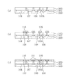
以下、本発明の一実施形態の変形例に係る強誘電体メモリ装置について、図3を参照しながら説明する。尚、該変形例においては、本発明の一実施形態と共通する部材については同一の符号を付すことにより、説明を省略する。
【0061】
本発明の一実施形態においては、図2に示すように、ワード線方向に並ぶ強誘電体キャパシタよりなるキャパシタ列同士の間には隙間が形成されており、該隙間に第2の層間絶縁膜116が埋め込まれている構造であったが、変形例においては、第3のコンタクトプラグ119を介することなくビット線方向に隣り合う一対のキャパシタ列同士の間には隙間が形成されておらず、該一対のキャパシタ列同士の間においては、絶縁性の第1の水素バリア膜111、段差緩和膜114及び第2の水素バリア膜115は連続している。
【0062】
本発明の一実施形態の変形例に係る強誘電体メモリ装置によると、絶縁性の第1の水素バリア膜111における、ビット線方向に隣り合う強誘電体キャパシタの下部電極109同士の間においてもパターニングする必要はない。このため、ビット線方向に隣り合う下部電極109同士の間隔をも小さくしてメモリセルアレイの面積を一層低減することができる。
【0063】
また、強誘電体メモリ装置の選択用トランジスタの近傍に、水素バリア膜が形成されていない領域が存在するため、金属配線を形成した後にトランジスタの特性を回復するために行なう水素雰囲気中での熱処理において、水素が選択トランジスタに拡散するための経路を確保することができる。特に、強誘電体キャパシタをトランジスタの上に形成するスタック型強誘電体メモリ装置の場合、水素が選択トランジスタに拡散するための経路をトランジスタ形成領域の近傍に設けることが可能となる。このため、金属配線を形成した後にトランジスタの特性を回復するために行なう水素雰囲気中での熱処理において、水素が選択トランジスタに拡散するための経路を確実に確保できるので、トランジスタの特性確保をも実現できる。
【0064】
以下、本発明の一実施形態に係る強誘電体メモリ装置の製造方法について、図4(a) 〜(c) 及び図5(a) 〜(c) を参照しながら説明する。
【0065】
まず、図4(a) に示すように、周知のSTI(Shallow Trench Isolation)技術等により、シリコンよりなる半導体基板100の表面部に素子分離領域101を形成した後、周知のCMOSプロセスにより、半導体基板100上における素子分離領域101で囲まれた領域に、ゲート絶縁膜を介してゲート電極102を形成し(図2を参照)、その後、半導体基板100の表面部におけるゲート電極102の両側に、ソース又はドレインとなる第1の高濃度不純物拡散層103A、103Bを形成すると共に、半導体基板100の表面部におけるメモリセルアレイの周縁部に第2の高濃度不純物拡散層104を形成する。これにより、ゲート電極102及び第1の不純物拡散層103A、103Bよりなる電界効果型トランジスタが形成される。
【0066】
次に、半導体基板100の上に、電界効果型トランジスタを覆うように、BPSG膜よりなる第1の層間絶縁膜105を形成した後、第1の層間絶縁膜105に、下端が第1の高濃度不純物拡散層103Aに接続される第1のコンタクトホール及び下端が第2の高濃度不純物拡散層104に接続される第2のコンタクトホールを形成する。次に、第1のコンタクトホール及び第2のコンタクトホールの壁面及び底面に、スパッタリング法による10nmの厚さを持つチタン膜とCVD法による10nmの厚さを持つ窒化チタン膜とを順次堆積した後、CVD法により、第1及び第2のコンタクトホールの内部並びに第1の層間絶縁膜105の上に全面に亘ってタングステン膜を堆積し、その後、CMP法により、タングステン膜における第1の層間絶縁膜105の上に露出している部分をポリッシュバックすることにより、第1のコンタクトプラグ106及び第2のコンタクトプラグ107を形成する。
【0067】
次に、スパッタリング法により、第1の層間絶縁膜105の上に例えば40nmの厚さを有するTiとAlとの合金の窒化物膜を堆積した後、スパッタリング法により、窒化物膜の上に、例えば100nmの厚さを有するIr膜、50nmの厚さを有するIrO2 膜及び100nmの厚さを有するPt膜よりなる積層膜を堆積し、その後、これら積層膜及び窒化物膜をパターニングして、図4(b) に示すように、TiとAlとの合金の窒化物膜よりなる導電性水素バリア膜108、Ir膜、IrO2 膜及びPt膜の積層膜よりなる下部電極109及び上部電極中継部110を形成する。尚、導電性水素バリア膜108となる膜としては、TiとAlとの合金の窒化物膜に代えて、TiとAlとの合金膜、TiとAlとの合金金の酸窒化物膜又はTiN膜を用いてもよい。
【0068】
次に、CVD法により、下部電極109、上部電極中継部110及び第1の層間絶縁膜105の上に全面に亘って、400nmの厚さを有するSi3N4膜を堆積した後、CMP法によりSiN膜を平坦化して、図4(c) に示すように、下部電極109同士の間及び下部電極109と上部電極中継部110との間に絶縁性の第1の水素バリア膜111を埋め込むと共に、絶縁性の第1の水素バリア膜111の上面を、下部電極109の上面及び上部電極中継部110の上面とほぼ面一にする。尚、絶縁性の第1の水素バリア膜111となる膜としては、Si3N4膜に代えて、SiON膜、Al2O3膜、TiO2 膜、又はTiとAlとの合金の酸化物膜若しくは酸窒化物膜を用いることができる。
【0069】
次に、図5(a) に示すように、スピン塗布法により、下部電極109、上部電極中継部110及び絶縁性の第1の水素バリア膜111の上に、例えばSBT膜よりなり100nmの厚さを有する強誘電体膜を堆積した後、該強誘電体膜をパターニングすることにより、ワード線方向に並ぶ下部電極109及び絶縁性の第1の水素バリア膜111の上に共通に形成され且つ上部電極中継部110の上に開口部を有する容量絶縁膜112を形成する。次に、スパッタリング法により、容量絶縁膜112の上に100nmの厚さを有するPt膜を堆積した後、該Pt膜をパターニングして、容量絶縁膜112の上に上部電極113を形成する。これにより、下部電極109、容量絶縁膜112及び上部電極113よりなる強誘電体キャパシタがワード線方向に並ぶキャパシタ列が形成されると共に、該キャパシタ列に共通の容量絶縁膜112及び上部電極113が形成される。
【0070】
次に、図5(b) に示すように、上部電極113及び絶縁性の第1の水素バリア膜111の上に全面に亘って150nmの厚さを有するNSG膜を堆積した後、該NSG膜を、該NSG膜がワード線方向に並ぶ強誘電体キャパシタよりなるキャパシタ列及び該キャパシタ列の端部に位置する上部電極中継部110を完全に覆うようにパターニングして、NSG膜よりなる段差緩和膜114を形成する。
【0071】
次に、段差緩和膜114及び絶縁性の第1の水素バリア膜111の上に全面に亘って、100nmの厚さを有する第2の水素バリア膜115を堆積した後、第2の水素バリア膜115及び絶縁性の第1の水素バリア膜111を、ワード線方向に並ぶ強誘電体キャパシタよりなるキャパシタ列及び該キャパシタ列の端部に位置する上部電極中継部110が覆われるようにパターニングする。このようにすると、パターニングされた第2の水素バリア膜115の周縁部とパターニングされた絶縁性の第1の水素バリア膜111の周縁部とが接続していることにより、ワード線方向に並ぶ強誘電体キャパシタよりなるキャパシタ列は導電性水素バリア膜108、第2の水素バリア膜115及び絶縁性の第1の水素バリア膜111により完全に覆われる。
【0072】
第2の水素バリア膜115としては、水素の侵入を防止できる膜、例えば、Si3N4膜、SiON膜、Al2O3 膜、TiO2膜、TiN膜若しくはTiとAlとの合金膜、又はTiとAlとの合金の酸化物膜、窒化物膜若しくは酸窒化物膜を用いることができる。
【0073】
ところで、段差緩和膜114は、パターニングにより形成された容量絶縁膜112及び上部電極113の周端部に形成される角張った段差を緩和して、第2の水素バリア膜115の容量絶縁膜112及び上部電極113の周端部におけるカバレッジを向上させるために設けられている。
【0074】
従って、第2の水素バリア膜115として、SiN膜、SiON膜、Al2O3 膜、TiO膜又はTiとAlとの合金の酸化物膜等のようにカバレッジに優れた膜を用いる場合には、段差緩和膜114を省略することも可能である。
【0075】
次に、図5(c) に示すように、第1の層間絶縁膜105の上に、パターニングされた第2の水素バリア膜115を覆うように、NSG膜よりなる第2の層間絶縁膜116を堆積した後、該第2の層間絶縁膜116を平坦化する。
【0076】
次に、第1の層間絶縁膜105及び第2の層間絶縁膜116に、第1の高濃度不純物拡散層103B(図2を参照)に接続される第3のコンタクトホール及び第2の高濃度不純物拡散層104に接続される第4のコンタクトホールを形成した後、第3のコンタクトホール及び第4のコンタクトホールにタングステン膜を埋め込んで、第3のコンタクトプラグ119(図2を参照)及び第4のコンタクトプラグ120を形成する。
【0077】
次に、第2の層間絶縁膜116の上にAl合金膜を堆積した後、該Al合金膜をパターニングして、第1の金属配線117及び第2の金属膜118を形成すると、本発明の一実施形態に係る強誘電体メモリ装置が得られる。
【0078】
尚、本発明の一実施形態においては、複数の強誘電体キャパシタのうち、ワード線方向に並ぶ複数の強誘電体キャパシタの下部電極109同士の間に絶縁性の第1の水素バリア膜111が埋め込まれ、ワード線方向に並ぶ複数の強誘電体キャパシタの下部電極109及び絶縁性の第1の水素バリア膜111の上に、ワード線方向に並ぶ複数の強誘電体キャパシタに共通の容量絶縁膜112が形成され、共通の容量絶縁膜112の上に、ワード線方向に並ぶ複数の強誘電体キャパシタに共通の上部電極113が形成され、共通の上部電極113を覆うように第2の水素バリア膜115が形成されていたが、これに代えて、複数の強誘電体キャパシタのうち、ビット線方向に並ぶ複数の強誘電体キャパシタの下部電極109同士の間に絶縁性の第1の水素バリア膜111が埋め込まれ、ビット線方向に並ぶ複数の強誘電体キャパシタの下部電極109及び絶縁性の第1の水素バリア膜111の上に、ビット線方向に並ぶ複数の強誘電体キャパシタに共通の容量絶縁膜112が形成され、共通の容量絶縁膜112の上に、ビット線方向に並ぶ複数の強誘電体キャパシタに共通の上部電極113が形成され、共通の上部電極113を覆うように第2の水素バリア膜115が形成されている構造であってもよい。
【0079】
【発明の効果】
本発明に係る強誘電体メモリ装置及びその製造方法によると、一方向に並ぶ複数の強誘電体キャパシタの下部電極同士の間に絶縁性の第1の水素バリア膜が埋め込まれているため、絶縁性の第1の水素バリア膜における、一方向に並ぶ複数の強誘電体キャパシタの下部電極同士の間の領域ではパターニングする必要はない。このため、パターニングを行なうためのマスクの位置ずれを考慮して、下部電極同士の間に寸法マージンを確保する必要がないので、強誘電体キャパシタ同士の間隔を狭くして、メモリセルアレイひいては強誘電体メモリ装置の面積を低減することができる。
【図面の簡単な説明】
【図1】本発明の一実施形態に係る強誘電体メモリ装置のワード線方向の断面図である。
【図2】本発明の一実施形態に係る強誘電体メモリ装置のビット線方向の断面図である。
【図3】本発明の一実施形態の変形例に係る強誘電体メモリ装置のビット線方向の断面図である。
【図4】 (a) 〜(c) は、本発明の一実施形態に係る強誘電体メモリ装置の製造方法の各工程を示す断面図である。
【図5】 (a) 〜(c) は、本発明の一実施形態に係る強誘電体メモリ装置の製造方法の各工程を示す断面図である。
【図6】従来の強誘電体メモリ装置の断面図である。
【符号の説明】
100 半導体基板
101 素子分離領域
102 ゲート電極
103A,103B 第1の高濃度不純物拡散層
104 第2の高濃度不純物拡散層
105 第1の層間絶縁膜
106 第1のコンタクトプラグ
107 第2のコンタクトプラグ
108 導電性水素バリア膜
109 下部電極
110 上部電極中継部
111 絶縁性の第1の水素バリア膜
112 容量絶縁膜
113 上部電極
114 段差緩和膜
115 第2の水素バリア膜
116 第2の層間絶縁膜
117 第1の金属配線
118 第2の金属配線
119 第3のコンタクトプラグ
120 第4のコンタクトプラグ[0001]
BACKGROUND OF THE INVENTION
The present invention includes a plurality of ferroelectric layers, which are sequentially formed on a semiconductor substrate, each including a lower electrode, a capacitive insulating film made of a ferroelectric film, and an upper electrode, and arranged in a matrix in the word line direction and the bit line direction. The present invention relates to a ferroelectric memory device including a body capacitor and a method for manufacturing the same.
[0002]
[Prior art]
In recent years, as a semiconductor memory device, for example, SrBi2Ta2O9(Hereinafter referred to as SBT) or Pb (Zr, Ti) OThreeA nonvolatile ferroelectric memory device having a capacitive insulating film made of a ferroelectric material film having a hysteresis characteristic such as PZT (hereinafter referred to as PZT) has been developed. Ferroelectric materials such as SBT and PZT used in such a ferroelectric memory device are ferroelectric oxides.
[0003]
For this reason, in the atmosphere containing hydrogen, which is performed to secure the characteristics of the MOS transistor formed on the semiconductor substrate after forming the aluminum wiring through the interlayer insulating film on the plurality of ferroelectric capacitors. In a CVD method performed to embed a tungsten film in a contact hole having a high aspect ratio accompanying heat treatment or miniaturization of a semiconductor memory device, if a ferroelectric oxide is exposed to a reducing atmosphere, particularly a hydrogen atmosphere, The dielectric oxide is reduced. For this reason, since the crystal composition of the ferroelectric oxide is destroyed, the insulating characteristics of the capacitive insulating film or the characteristics of the ferroelectric oxide are greatly deteriorated.
[0004]
Therefore, even if the ferroelectric capacitor is formed and then subjected to a heat treatment in a hydrogen atmosphere, the capacitive insulating film of the ferroelectric capacitor is not exposed to hydrogen and reduced. As described above, a hydrogen barrier film that prevents hydrogen from entering the capacitor insulating film is formed so as to cover the ferroelectric capacitor.
[0005]
However, when a hydrogen barrier film is provided between a ferroelectric capacitor and an interlayer insulating film formed on the ferroelectric capacitor, in order to block hydrogen from entering from the horizontal direction, It is necessary to make the area at least several μm larger than the area of the ferroelectric capacitor. In addition, since the hydrogen barrier film is also formed on the contact plug embedded in the interlayer insulating film, when the contact plug is formed of a tungsten film formed by a CVD method, the capacitive insulating film included in the hydrogen barrier film The effect of preventing the entry of hydrogen into the water is reduced.
[0006]
In particular, in recent years, the area of ferroelectric capacitors has been reduced (1 μm) with the miniaturization of ferroelectric memory devices.2However, for the reason described above, it is not possible to reliably prevent hydrogen from entering the capacitor insulating film simply by covering the ferroelectric capacitor with the hydrogen barrier film.
[0007]
Japanese Patent Application Laid-Open No. 11-135736 proposes a ferroelectric memory device having a structure as shown in FIG.
[0008]
Hereinafter, a ferroelectric memory device shown in FIG. 6 will be described as a conventional example.
[0009]
On the surface portion of the
[0010]
A first interlayer
[0011]
A second
[0012]
[Problems to be solved by the invention]
As described above, the ferroelectric capacitor is completely covered with the first insulating
[0013]
However, in the conventional ferroelectric memory device, the side portion of the second insulating
[0014]
Therefore, it is necessary to increase the thickness of the second insulating
[0015]
For this reason, since it is necessary to increase the interval between the ferroelectric capacitors, there is a problem that it is difficult to miniaturize the ferroelectric memory device.
[0016]
In view of the foregoing, it is an object of the present invention to achieve both a reliable prevention of a situation where hydrogen enters a capacitive insulating film of a ferroelectric capacitor and a miniaturization of a ferroelectric memory device.
[0017]
[Means for Solving the Problems]
In order to achieve the above object, a ferroelectric memory device according to
Provided to cover the plurality of upper electrodes, and Si3N4Film, SiON film, Al2O3Film, TiO2A second hydrogen barrier film comprising a film, a TiN film or an alloy film of Ti and Al, or an oxide film of a Ti and Al alloy, a nitride film or an oxynitride film,
The second hydrogen barrier film is formed separately for each capacitor row composed of the plurality of ferroelectric capacitors arranged in one of the word line direction and the bit line direction,
Of the plurality of ferroelectric capacitors, embedded between the lower electrodes of the plurality of ferroelectric capacitors arranged in one direction.The upper surface is substantially flush with the upper surface of the lower electrode.An insulating first hydrogen barrier film;
A conductive hydrogen barrier film formed between the contact plug formed in the interlayer insulating film and the lower electrode;
The second hydrogen barrier filmThe periphery ofSaid first hydrogen barrierMembraneTopWhenConnected,
Line up in one directionSaidpluralFerroelectric capacitorCapacitor array consisting ofIs completely covered by the second hydrogen barrier film, the first hydrogen barrier film, and the conductive hydrogen barrier film.The
[0018]
According to the ferroelectric memory device of the first aspect of the present invention, the upper electrode is covered.SecondSince the hydrogen barrier film is formed, when heat treatment is performed in a hydrogen atmosphere after the ferroelectric capacitor is formed, hydrogen that enters from the upper side to the capacitive insulating film of the ferroelectric capacitor is prevented. Therefore, the reduction of the ferroelectric film constituting the capacitive insulating film can be prevented.
Also, between the lower electrodes of the plurality of ferroelectric capacitors arranged in one of the word line direction and the bit line direction.FirstEmbedded with an insulating hydrogen barrier filmFirstIn the insulating hydrogen barrier film, it is not necessary to pattern the region between the lower electrodes of the plurality of ferroelectric capacitors arranged in one direction. For this reason, it is not necessary to secure a dimensional margin between the lower electrodes in consideration of the positional deviation of the mask for patterning. Therefore, the interval between the ferroelectric capacitors is narrowed, and the memory cell array and the ferroelectric layer are thus formed. The area of the body memory device can be reduced.
[0019]
A ferroelectric memory device according to a second aspect of the present invention includes a lower electrode, a capacitor insulating film made of a ferroelectric film, and an upper electrode sequentially formed on an interlayer insulating film on a semiconductor substrate, and a word line A ferroelectric memory device comprising a plurality of ferroelectric capacitors arranged in a direction and a bit line direction,
Provided to cover the plurality of upper electrodes, and Si3N4Film, SiON film, Al2O3Film, TiO2A second hydrogen barrier film comprising a film, a TiN film or an alloy film of Ti and Al, or an oxide film of a Ti and Al alloy, a nitride film or an oxynitride film,
The second hydrogen barrier film is arranged in the other direction of the word line direction and the bit line direction in the capacitor row composed of the plurality of ferroelectric capacitors arranged in one direction of the word line direction and the bit line direction. Formed to cover a pair of adjacent capacitor rows,
Of the plurality of ferroelectric capacitors, theA pair of capacitor rowsEmbedded between the lower electrodes of a plurality of ferroelectric capacitors.The upper surface is substantially flush with the upper surface of the lower electrode.An insulating first hydrogen barrier film;
A conductive hydrogen barrier film formed between the contact plug formed in the interlayer insulating film and the lower electrode;
The second hydrogen barrier filmThe periphery ofSaid first hydrogen barrierMembraneTopWhenConnected,
SaidpluralFerroelectric capacitorThe pair of capacitor arraysIs completely covered by the second hydrogen barrier film, the first hydrogen barrier film, and the conductive hydrogen barrier film.The
[0021]
According to the ferroelectric memory device of the second aspect of the present invention,SecondIn the hydrogen barrier film, it is not necessary to secure a dimensional margin between a pair of capacitor rows made of a plurality of ferroelectric capacitors arranged in one direction. As a result, the area of the ferroelectric memory device can be reduced. In addition, since there is a region where the hydrogen barrier film is not formed in the vicinity of the selection transistor of the ferroelectric memory device, heat treatment in a hydrogen atmosphere is performed in order to restore the characteristics of the transistor after forming the metal wiring. , A path for hydrogen to diffuse into the selection transistor can be secured.
[0022]
A ferroelectric memory device according to claim 3 of the present invention is the ferroelectric memory device according to
[0028]
Claims of the invention4The ferroelectric memory device according to claim 3, wherein the common upper electrode and the ferroelectric memory device according to claim 3.SecondIt is preferable that a step-relief film formed between the hydrogen barrier film and the step formed on the peripheral edge of the common upper electrode is formed.
[0029]
In this way, the angular step formed on the peripheral edge of the patterned upper electrode is relaxed,SecondThe coverage at the peripheral edge of the upper electrode of the hydrogen barrier film can be improved.
[0030]
Claims of the invention5According to a ferroelectric memory device according to
[0032]
Claims of the invention6According to a ferroelectric memory device according to claim1 or 2In the ferroelectric memory device according to the above,ConductivityAs the hydrogen barrier film, an alloy film of Ti and Al, a nitride film or oxynitride film of an alloy of Ti and Al, or a TiN film can be used.
[0033]
A manufacturing method of a ferroelectric memory device according to claim 7 of the present invention includes a lower electrode, a capacitor insulating film made of a ferroelectric film, and an upper electrode sequentially formed on an interlayer insulating film on a semiconductor substrate. A method of manufacturing a ferroelectric memory device having a plurality of ferroelectric capacitors arranged in a word line direction and a bit line direction,
Forming a conductive hydrogen barrier film on the contact plug formed in the interlayer insulating film;
SaidConductive hydrogen barrier filmForming a lower electrode of the plurality of ferroelectric capacitors,
After depositing an insulating first hydrogen barrier film on the interlayer insulating film and the lower electrode, the first hydrogen barrier film is planarized, and the word line direction of the plurality of ferroelectric capacitors is And the first hydrogen barrier film embedded between the lower electrodes of the plurality of ferroelectric capacitors arranged in one direction of the bit line direction, and the upper surface of the lower electrode and the first hydrogen barrier film Forming the upper surface of the substrate substantially flush with the upper surface;
Forming a capacitive insulating film on the lower electrode;
Forming an upper electrode on the capacitive insulating film;
Si3N4Film, SiON film, Al2O3Film, TiO2A second hydrogen barrier film made of a film, a TiN film or an alloy film of Ti and Al, or an oxide film, nitride film or oxynitride film of Ti and Al, covering the plurality of upper electrodes. And of the word line direction and bit line directionSaidFormed separately for each capacitor row composed of the plurality of ferroelectric capacitors arranged in one direction.In addition, the peripheral portion is formed so as to be connected to the upper surface of the first hydrogen barrier film.With processes,
in frontA capacitor row composed of the plurality of ferroelectric capacitors arranged in the same direction is completely covered with the second hydrogen barrier film, the first hydrogen barrier film, and the conductive hydrogen barrier film.
[0034]
Claims of the invention7According to the manufacturing method of the ferroelectric memory device according to theSecondTherefore, when a heat treatment in a hydrogen atmosphere is performed after the formation of the ferroelectric capacitor, it penetrates into the capacitive insulating film of the ferroelectric capacitor from above. Since hydrogen can be prevented, the reduction of the ferroelectric film constituting the capacitive insulating film can be prevented.
Also, between the lower electrodes of a plurality of ferroelectric capacitors arranged in one directionFirstEmbedded with an insulating hydrogen barrier filmFirstIn the insulating hydrogen barrier film, it is not necessary to pattern the region between the lower electrodes of the plurality of ferroelectric capacitors arranged in one direction. For this reason, it is not necessary to secure a dimensional margin between the lower electrodes in consideration of the positional deviation of the mask for patterning. Therefore, the interval between the ferroelectric capacitors is narrowed, and the memory cell array and the ferroelectric layer are thus formed. The area of the body memory device can be reduced.
[0036]
A method of manufacturing a ferroelectric memory device according to an eighth aspect of the present invention includes a lower electrode, a capacitor insulating film made of a ferroelectric film, and an upper electrode sequentially formed on an interlayer insulating film on a semiconductor substrate. A method of manufacturing a ferroelectric memory device having a plurality of ferroelectric capacitors arranged in a word line direction and a bit line direction,
Forming a conductive hydrogen barrier film on the contact plug formed in the interlayer insulating film;
SaidConductive hydrogen barrier filmForming a lower electrode of the plurality of ferroelectric capacitors,
After depositing an insulating first hydrogen barrier film on the interlayer insulating film and the lower electrode, the first hydrogen barrier film is planarized, and the word line direction of the plurality of ferroelectric capacitors is And a plurality of ferroelectric capacitors of a pair of capacitor rows adjacent to each other in the word line direction and the bit line direction among the plurality of ferroelectric capacitors arranged in one direction of the bit line direction. Embedding the first hydrogen barrier film between the lower electrodes of the body capacitor to form an upper surface of the lower electrode and an upper surface of the first hydrogen barrier film substantially flush with each other;
Forming a capacitive insulating film on the lower electrode;
Forming an upper electrode on the capacitive insulating film;
Si3N4Film, SiON film, Al2O3Film, TiO2Film, TiN film or alloy film of Ti and Al, or oxide film, nitride film or oxynitride film of Ti and Al alloyConsist ofA second hydrogen barrier film covering the plurality of upper electrodes, and in the word line direction and the bit line direction;SaidOf the capacitor rows formed of the plurality of ferroelectric capacitors arranged in one direction, the capacitor rows are formed so as to cover a pair of capacitor rows adjacent to each other in the word line direction and the bit line direction.In addition, the peripheral portion is formed so as to be connected to the upper surface of the first hydrogen barrier film.With processes,
in frontConsisting of multiple ferroelectric capacitorsThe pair ofThe capacitor array is completely covered with the second hydrogen barrier film, the first hydrogen barrier film, and the conductive hydrogen barrier film.
[0037]
If you do this,SecondIn the hydrogen barrier film, it is not necessary to secure a dimensional margin between a pair of capacitor rows made of a plurality of ferroelectric capacitors arranged in one direction. As a result, the area of the ferroelectric memory device can be reduced. In addition, since there is a region where the hydrogen barrier film is not formed in the vicinity of the selection transistor of the ferroelectric memory device, heat treatment in a hydrogen atmosphere is performed in order to restore the characteristics of the transistor after forming the metal wiring. , A path for hydrogen to diffuse into the selection transistor can be secured.
[0044]
The present inventionClaim 9A method for manufacturing a ferroelectric memory device according to the present invention includes a step of forming a common upper electrode,SecondDuring the process of forming the hydrogen barrier film, the common upper electrode andFirstIt is preferable to further include a step of forming a step mitigating film interposed between the hydrogen barrier film and mitigating the step formed on the peripheral edge of the common upper electrode.
[0045]
In this way, the angular step formed at the peripheral end of the patterned upper electrode is alleviated, so that the secondofThe coverage at the peripheral edge of the upper electrode of the hydrogen barrier film can be improved.
[0046]
Claims of the invention10In the method of manufacturing a ferroelectric memory device according to the above,FirstAs a hydrogen barrier film, SiThreeNFourFilm, SiON film, Al2OThreeFilm, TiO2 A film, or an oxide film or oxynitride of an alloy of Ti and Al can be used.
[0048]
Claims of the invention11In the method of manufacturing a ferroelectric memory device according to the above,ConductivityAs the hydrogen barrier film, an alloy film of Ti and Al, a nitride film or oxynitride film of an alloy of Ti and Al, or a TiN film can be used.
[0049]
DETAILED DESCRIPTION OF THE INVENTION
Hereinafter, the structure of a ferroelectric memory device according to an embodiment of the present invention will be described with reference to FIGS.
[0050]
A ferroelectric memory device according to an embodiment of the present invention includes a memory cell array including a plurality of memory cells arranged in a matrix in a word line direction and a bit line direction. FIG. 1 shows a cross-sectional structure of a surface parallel to the word line in the ferroelectric memory device, and FIG. 2 shows a cross-sectional structure of a surface parallel to the bit line in the ferroelectric memory device.
[0051]
As shown in FIGS. 1 and 2, an
[0052]
A first
[0053]
On top of the first
[0054]
On the first
[0055]
[0056]
On the
[0057]
On the first
[0058]
According to the ferroelectric memory device in accordance with the embodiment of the present invention, there is an insulating property between the
[0059]
In addition, a capacitor row composed of a plurality of ferroelectric capacitors arranged in the word line direction is electrically conductive.
[0060]
Hereinafter, a ferroelectric memory device according to a modification of one embodiment of the present invention will be described with reference to FIG. In this modification, members common to one embodiment of the present invention are denoted by the same reference numerals, and description thereof is omitted.
[0061]
In one embodiment of the present invention, as shown in FIG. 2, a gap is formed between capacitor rows made of ferroelectric capacitors arranged in the word line direction, and a second interlayer insulating film is formed in the gap. 116 is embedded, but in the modified example, no gap is formed between a pair of capacitor columns adjacent in the bit line direction without the
[0062]
According to the ferroelectric memory device according to the modification of the embodiment of the present invention, the insulatingFirstIt is not necessary to perform patterning between the
[0063]
In addition, since there is a region where the hydrogen barrier film is not formed in the vicinity of the selection transistor of the ferroelectric memory device, heat treatment in a hydrogen atmosphere is performed in order to restore the characteristics of the transistor after forming the metal wiring. , A path for hydrogen to diffuse into the selection transistor can be secured. In particular, in the case of a stacked ferroelectric memory device in which a ferroelectric capacitor is formed on a transistor, a path for hydrogen to diffuse into the selection transistor can be provided in the vicinity of the transistor formation region. For this reason, in heat treatment in a hydrogen atmosphere to restore the transistor characteristics after forming the metal wiring, it is possible to reliably secure a path for hydrogen to diffuse into the selected transistor, thus ensuring the transistor characteristics. it can.
[0064]
A method for manufacturing a ferroelectric memory device according to an embodiment of the present invention will be described below with reference to FIGS. 4 (a) to (c) and FIGS. 5 (a) to (c).
[0065]
First, as shown in FIG. 4A, an
[0066]
Next, a first
[0067]
Next, after depositing a nitride film of an alloy of Ti and Al having a thickness of, for example, 40 nm on the first
[0068]
Next, a Si3N4 film having a thickness of 400 nm is deposited on the entire surface of the
[0069]
Next, as shown in FIG. 5A, the
[0070]
Next, as shown in FIG. 5B, the
[0071]
Next, the
[0072]
SecondAs the
[0073]
By the way, the
[0074]
Therefore,SecondAs the
[0075]
Next, as shown in FIG. 5C, the first
[0076]
Next, a third contact hole and a second high concentration connected to the first high concentration
[0077]
Next, after depositing an Al alloy film on the second
[0078]
In one embodiment of the present invention, among the plurality of ferroelectric capacitors, there is an insulating property between the
[0079]
【The invention's effect】
According to the ferroelectric memory device and the method of manufacturing the same according to the present invention, an insulating property is provided between the lower electrodes of a plurality of ferroelectric capacitors arranged in one direction.FirstBecause of the embedded hydrogen barrier film,FirstIn the hydrogen barrier film, it is not necessary to pattern the region between the lower electrodes of the plurality of ferroelectric capacitors arranged in one direction. For this reason, it is not necessary to secure a dimensional margin between the lower electrodes in consideration of the positional deviation of the mask for patterning. Therefore, the interval between the ferroelectric capacitors is narrowed, and the memory cell array and the ferroelectric layer are thus formed. The area of the body memory device can be reduced.
[Brief description of the drawings]
FIG. 1 is a sectional view of a ferroelectric memory device according to an embodiment of the present invention in a word line direction.
FIG. 2 is a cross-sectional view in the bit line direction of a ferroelectric memory device according to an embodiment of the present invention.
FIG. 3 is a cross-sectional view in the bit line direction of a ferroelectric memory device according to a modification of one embodiment of the present invention.
FIGS. 4A to 4C are cross-sectional views illustrating respective steps of a method for manufacturing a ferroelectric memory device according to an embodiment of the present invention. FIGS.
FIGS. 5A to 5C are cross-sectional views showing respective steps of a method for manufacturing a ferroelectric memory device according to an embodiment of the present invention. FIGS.
FIG. 6 is a cross-sectional view of a conventional ferroelectric memory device.
[Explanation of symbols]
100 Semiconductor substrate
101 Element isolation region
102 Gate electrode
103A, 103B first high-concentration impurity diffusion layers
104 Second high-concentration impurity diffusion layer
105 First interlayer insulating film
106 First contact plug
107 second contact plug
108 conductivityWaterElementary barrier film
109 Lower electrode
110 Upper electrode relay part
111 insulatingFirstHydrogen barrier film
112 Capacitance insulation film
113 Upper electrode
114 Step relief film
115SecondHydrogen barrier film
116 Second interlayer insulating film
117 first metal wiring
118 Second metal wiring
119 Third contact plug
120 Fourth contact plug
Claims (11)
複数の前記上部電極を覆うように設けられ、Si3N4膜、SiON膜、Al2O3膜、TiO2膜、TiN膜若しくはTiとAlとの合金膜、又はTiとAlとの合金の酸化物膜、窒化物膜若しくは酸窒化物膜よりなる第2の水素バリア膜を備え、
前記第2の水素バリア膜は、ワード線方向及びビット線方向のうちの一方向に並ぶ前記複数の強誘電体キャパシタよりなるキャパシタ列毎に分離して形成され、
前記複数の強誘電体キャパシタのうち、前記一方向に並ぶ複数の強誘電体キャパシタの前記下部電極同士の間に埋め込まれ、上面が前記下部電極の上面とほぼ面一に形成された絶縁性の第1の水素バリア膜と、
前記層間絶縁膜に形成されているコンタクトプラグと前記下部電極との間に形成されている導電性水素バリア膜とをさらに備え、
前記第2の水素バリア膜の周縁部は、前記第1の水素バリア膜の上面と接続され、
前記一方向に並ぶ前記複数の強誘電体キャパシタよりなるキャパシタ列は、前記第2の水素バリア膜、前記第1の水素バリア膜及び前記導電性水素バリア膜によって完全に覆われていることを特徴とする強誘電体メモリ装置。A plurality of ferroelectric capacitors having a lower electrode, a capacitor insulating film made of a ferroelectric film, and an upper electrode sequentially formed on an interlayer insulating film on a semiconductor substrate, and arranged in a word line direction and a bit line direction A ferroelectric memory device comprising:
It is provided so as to cover the plurality of upper electrodes, and is made of an Si 3 N 4 film, an SiON film, an Al 2 O 3 film, a TiO 2 film, a TiN film, an alloy film of Ti and Al, or an alloy of Ti and Al A second hydrogen barrier film made of an oxide film, a nitride film or an oxynitride film;
The second hydrogen barrier film is formed separately for each capacitor row composed of the plurality of ferroelectric capacitors arranged in one of the word line direction and the bit line direction,
Of the plurality of ferroelectric capacitors, an insulating material embedded between the lower electrodes of the plurality of ferroelectric capacitors arranged in one direction and having an upper surface substantially flush with the upper surface of the lower electrode . A first hydrogen barrier film;
A conductive hydrogen barrier film formed between the contact plug formed in the interlayer insulating film and the lower electrode;
A peripheral portion of the second hydrogen barrier film is connected to an upper surface of the first hydrogen barrier film ,
A capacitor row composed of the plurality of ferroelectric capacitors arranged in one direction is completely covered with the second hydrogen barrier film, the first hydrogen barrier film, and the conductive hydrogen barrier film. A ferroelectric memory device.
複数の前記上部電極を覆うように設けられ、Si3N4膜、SiON膜、Al2O3膜、TiO2膜、TiN膜若しくはTiとAlとの合金膜、又はTiとAlとの合金の酸化物膜、窒化物膜若しくは酸窒化物膜よりなる第2の水素バリア膜を備え、
前記第2の水素バリア膜は、ワード線方向及びビット線方向のうちの一方向に並ぶ前記複数の強誘電体キャパシタよりなるキャパシタ列のうち、ワード線方向及びビット線方向のうちの他方向に隣り合う一対のキャパシタ列を覆うように形成され、
前記複数の強誘電体キャパシタのうち、前記一対のキャパシタ列の前記複数の強誘電体キャパシタの前記下部電極同士の間に埋め込まれ、上面が前記下部電極の上面とほぼ面一に形成された絶縁性の第1の水素バリア膜と、
前記層間絶縁膜に形成されているコンタクトプラグと前記下部電極との間に形成されている導電性水素バリア膜とをさらに備え、
前記第2の水素バリア膜の周縁部は、前記第1の水素バリア膜の上面と接続され、
前記複数の強誘電体キャパシタよりなる前記一対のキャパシタ列は、前記第2の水素バリア膜、前記第1の水素バリア膜及び前記導電性水素バリア膜によって完全に覆われていることを特徴とする強誘電体メモリ装置。A plurality of ferroelectric capacitors having a lower electrode, a capacitor insulating film made of a ferroelectric film, and an upper electrode sequentially formed on an interlayer insulating film on a semiconductor substrate, and arranged in a word line direction and a bit line direction A ferroelectric memory device comprising:
It is provided so as to cover the plurality of upper electrodes, and is made of an Si 3 N 4 film, an SiON film, an Al 2 O 3 film, a TiO 2 film, a TiN film, an alloy film of Ti and Al, or an alloy of Ti and Al A second hydrogen barrier film made of an oxide film, a nitride film or an oxynitride film;
The second hydrogen barrier film is arranged in the other direction of the word line direction and the bit line direction in the capacitor row composed of the plurality of ferroelectric capacitors arranged in one direction of the word line direction and the bit line direction. Formed to cover a pair of adjacent capacitor rows,
Of the plurality of ferroelectric capacitors, an insulating layer embedded between the lower electrodes of the plurality of ferroelectric capacitors of the pair of capacitor rows and having an upper surface substantially flush with an upper surface of the lower electrode A first hydrogen barrier film,
A conductive hydrogen barrier film formed between the contact plug formed in the interlayer insulating film and the lower electrode;
A peripheral portion of the second hydrogen barrier film is connected to an upper surface of the first hydrogen barrier film ,
The pair of capacitor arrays including the plurality of ferroelectric capacitors are completely covered with the second hydrogen barrier film, the first hydrogen barrier film, and the conductive hydrogen barrier film. Ferroelectric memory device.
前記層間絶縁膜に形成されているコンタクトプラグの上に導電性水素バリア膜を形成する工程と、
前記導電性水素バリア膜の上に、前記複数の強誘電体キャパシタの下部電極を形成する工程と、
前記層間絶縁膜及び前記下部電極の上に絶縁性の第1の水素バリア膜を堆積した後、該第1の水素バリア膜を平坦化して、前記複数の強誘電体キャパシタのうち、ワード線方向及びビット線方向のうちの一方向に並ぶ前記複数の強誘電体キャパシタの前記下部電極同士の間に前記第1の水素バリア膜を埋め込んで、前記下部電極の上面と前記第1の水素バリア膜の上面をほぼ面一に形成する工程と、
前記下部電極上に容量絶縁膜を形成する工程と、
前記容量絶縁膜の上に上部電極を形成する工程と、
Si3N4膜、SiON膜、Al2O3膜、TiO2膜、TiN膜若しくはTiとAlとの合金膜、又はTiとAlとの合金の酸化物膜、窒化物膜若しくは酸窒化物膜よりなる第2の水素バリア膜を、複数の前記上部電極を覆い、かつ、ワード線方向及びビット線方向のうちの前記一方向に並ぶ前記複数の強誘電体キャパシタよりなるキャパシタ列毎に分離して形成するとともに、周縁部は前記第1の水素バリア膜の上面と接続するように形成する工程とを備え、
前記一方向に並ぶ前記複数の強誘電体キャパシタよりなるキャパシタ列は、前記第2の水素バリア膜、前記第1の水素バリア膜及び前記導電性水素バリア膜によって完全に覆われていることを特徴とする強誘電体メモリ装置の製造方法。A plurality of ferroelectric capacitors having a lower electrode, a capacitor insulating film made of a ferroelectric film, and an upper electrode sequentially formed on an interlayer insulating film on a semiconductor substrate, and arranged in a word line direction and a bit line direction A method for manufacturing a ferroelectric memory device comprising:
Forming a conductive hydrogen barrier film on the contact plug formed in the interlayer insulating film;
Forming lower electrodes of the plurality of ferroelectric capacitors on the conductive hydrogen barrier film ;
After depositing an insulating first hydrogen barrier film on the interlayer insulating film and the lower electrode, the first hydrogen barrier film is planarized, and the word line direction of the plurality of ferroelectric capacitors is And the first hydrogen barrier film embedded between the lower electrodes of the plurality of ferroelectric capacitors arranged in one direction of the bit line direction, and the upper surface of the lower electrode and the first hydrogen barrier film Forming the upper surface of the substrate substantially flush with the upper surface;
Forming a capacitive insulating film on the lower electrode;
Forming an upper electrode on the capacitive insulating film;
Si 3 N 4 film, SiON film, Al 2 O 3 film, TiO 2 film, TiN film, Ti-Al alloy film, Ti-Al alloy oxide film, nitride film, or oxynitride film more it becomes the second hydrogen barrier film covers a plurality of the upper electrode, and separated for each capacitor row formed from said plurality of ferroelectric capacitors arranged in the one direction of the word line direction and the bit line direction And forming a peripheral edge portion so as to be connected to the upper surface of the first hydrogen barrier film ,
Wherein the plurality of ferroelectric capacitors column consisting of a capacitor arranged in front Symbol one direction, the second hydrogen barrier film, that is completely covered by the first hydrogen barrier film and said conductive hydrogen barrier film A method of manufacturing a ferroelectric memory device characterized by the following.
前記層間絶縁膜に形成されているコンタクトプラグの上に導電性水素バリア膜を形成する工程と、
前記導電性水素バリア膜の上に、前記複数の強誘電体キャパシタの下部電極を形成する工程と、
前記層間絶縁膜及び前記下部電極の上に絶縁性の第1の水素バリア膜を堆積した後、該第1の水素バリア膜を平坦化して、前記複数の強誘電体キャパシタのうち、ワード線方向及びビット線方向のうちの一方向に並ぶ前記複数の強誘電体キャパシタよりなるキャパシタ列のうち、ワード線方向及びビット線方向のうちの他方向に隣り合う一対のキャパシタ列の前記複数の強誘電体キャパシタの前記下部電極同士の間に前記第1の水素バリア膜を埋め込んで、前記下部電極の上面と前記第1の水素バリア膜の上面をほぼ面一に形成する工程と、
前記下部電極上に容量絶縁膜を形成する工程と、
前記容量絶縁膜の上に上部電極を形成する工程と、
Si3N4膜、SiON膜、Al2O3膜、TiO2膜、TiN膜若しくはTiとAlとの合金膜、又はTiとAlとの合金の酸化物膜、窒化物膜若しくは酸窒化物膜よりなる第2の水素バリア膜を、複数の前記上部電極を覆い、かつ、ワード線方向及びビット線方向のうちの前記一方向に並ぶ前記複数の強誘電体キャパシタよりなるキャパシタ列のうち、ワード線方向及びビット線方向のうちの他方向に隣り合う一対のキャパシタ列を覆うように形成するとともに、周縁部は前記第1の水素バリア膜の上面と接続するように形成する工程とを備え、
前記複数の強誘電体キャパシタよりなる前記一対のキャパシタ列は、前記第2の水素バリア膜、前記第1の水素バリア膜及び前記導電性水素バリア膜によって完全に覆われていることを特徴とする強誘電体メモリ装置の製造方法。A plurality of ferroelectric capacitors having a lower electrode, a capacitor insulating film made of a ferroelectric film, and an upper electrode sequentially formed on an interlayer insulating film on a semiconductor substrate, and arranged in a word line direction and a bit line direction A method for manufacturing a ferroelectric memory device comprising:
Forming a conductive hydrogen barrier film on the contact plug formed in the interlayer insulating film;
Forming lower electrodes of the plurality of ferroelectric capacitors on the conductive hydrogen barrier film ;
After depositing an insulating first hydrogen barrier film on the interlayer insulating film and the lower electrode, the first hydrogen barrier film is planarized, and the word line direction of the plurality of ferroelectric capacitors is And a plurality of ferroelectric capacitors of a pair of capacitor rows adjacent to each other in the word line direction and the bit line direction among the plurality of ferroelectric capacitors arranged in one direction of the bit line direction. Embedding the first hydrogen barrier film between the lower electrodes of the body capacitor to form an upper surface of the lower electrode and an upper surface of the first hydrogen barrier film substantially flush with each other;
Forming a capacitive insulating film on the lower electrode;
Forming an upper electrode on the capacitive insulating film;
Si 3 N 4 film, SiON film, Al 2 O 3 film, TiO 2 film, TiN film, Ti-Al alloy film, Ti-Al alloy oxide film, nitride film, or oxynitride film more it becomes the second hydrogen barrier film covers a plurality of the upper electrode, and among the plurality of intensity capacitor column comprising a dielectric capacitor arranged in the one direction of the word line direction and the bit line direction, word Forming a pair of capacitor rows adjacent to each other in the line direction and the bit line direction, and forming a peripheral edge portion to connect to the upper surface of the first hydrogen barrier film ,
Said pair of capacitor rows before Symbol comprising a plurality of ferroelectric capacitors, and characterized by being completely covered by the second hydrogen barrier film, said first hydrogen barrier film and said conductive hydrogen barrier film A method for manufacturing a ferroelectric memory device.
Priority Applications (1)
| Application Number | Priority Date | Filing Date | Title |
|---|---|---|---|
| JP2002224451A JP3962296B2 (en) | 2001-09-27 | 2002-08-01 | Ferroelectric memory device and manufacturing method thereof |
Applications Claiming Priority (3)
| Application Number | Priority Date | Filing Date | Title |
|---|---|---|---|
| JP2001-296855 | 2001-09-27 | ||
| JP2001296855 | 2001-09-27 | ||
| JP2002224451A JP3962296B2 (en) | 2001-09-27 | 2002-08-01 | Ferroelectric memory device and manufacturing method thereof |
Related Child Applications (1)
| Application Number | Title | Priority Date | Filing Date |
|---|---|---|---|
| JP2004355243A Division JP4351990B2 (en) | 2001-09-27 | 2004-12-08 | Ferroelectric memory device and manufacturing method thereof |
Publications (3)
| Publication Number | Publication Date |
|---|---|
| JP2003174145A JP2003174145A (en) | 2003-06-20 |
| JP2003174145A5 JP2003174145A5 (en) | 2005-05-26 |
| JP3962296B2 true JP3962296B2 (en) | 2007-08-22 |
Family
ID=26623091
Family Applications (1)
| Application Number | Title | Priority Date | Filing Date |
|---|---|---|---|
| JP2002224451A Expired - Lifetime JP3962296B2 (en) | 2001-09-27 | 2002-08-01 | Ferroelectric memory device and manufacturing method thereof |
Country Status (1)
| Country | Link |
|---|---|
| JP (1) | JP3962296B2 (en) |
Families Citing this family (12)
| Publication number | Priority date | Publication date | Assignee | Title |
|---|---|---|---|---|
| JP4636834B2 (en) * | 2002-11-13 | 2011-02-23 | パナソニック株式会社 | Semiconductor device and manufacturing method thereof |
| CN1284242C (en) | 2002-11-13 | 2006-11-08 | 松下电器产业株式会社 | Semiconductor device and method for fabricating the same |
| JP4549947B2 (en) * | 2003-05-27 | 2010-09-22 | パナソニック株式会社 | Semiconductor device |
| JP3935475B2 (en) | 2004-03-18 | 2007-06-20 | 松下電器産業株式会社 | Semiconductor device and manufacturing method thereof |
| US8552484B2 (en) | 2004-07-02 | 2013-10-08 | Fujitsu Semiconductor Limited | Semiconductor device and method for fabricating the same |
| JP4042730B2 (en) | 2004-09-02 | 2008-02-06 | セイコーエプソン株式会社 | Ferroelectric memory and manufacturing method thereof |
| JP2006108152A (en) * | 2004-09-30 | 2006-04-20 | Oki Electric Ind Co Ltd | Semiconductor memory device |
| JP4422644B2 (en) | 2005-03-30 | 2010-02-24 | 富士通マイクロエレクトロニクス株式会社 | Manufacturing method of semiconductor device |
| JP2006302987A (en) * | 2005-04-18 | 2006-11-02 | Nec Electronics Corp | Semiconductor device and its manufacturing method |
| JP4756915B2 (en) * | 2005-05-31 | 2011-08-24 | Okiセミコンダクタ株式会社 | Ferroelectric memory device and manufacturing method thereof |
| JP4930371B2 (en) | 2005-06-17 | 2012-05-16 | 富士通セミコンダクター株式会社 | Semiconductor device and manufacturing method thereof |
| JP4557903B2 (en) * | 2006-02-10 | 2010-10-06 | パナソニック株式会社 | Semiconductor device and manufacturing method thereof |
-
2002
- 2002-08-01 JP JP2002224451A patent/JP3962296B2/en not_active Expired - Lifetime
Also Published As
| Publication number | Publication date |
|---|---|
| JP2003174145A (en) | 2003-06-20 |
Similar Documents
| Publication | Publication Date | Title |
|---|---|---|
| US7531863B2 (en) | Semiconductor device and method of fabricating the same | |
| US7560760B2 (en) | Ferroelectric memory devices having expanded plate lines | |
| US6943398B2 (en) | Semiconductor device and method for fabricating the same | |
| JPH1168041A (en) | Structure for semiconductor device and its manufacture | |
| US6972449B2 (en) | Ferroelectric memory having a hydrogen barrier film which continuously covers a plurality of capacitors in a capacitor line | |
| JP3657925B2 (en) | Semiconductor device and manufacturing method thereof | |
| JP3962296B2 (en) | Ferroelectric memory device and manufacturing method thereof | |
| US20060183252A1 (en) | Ferroelectric memory devices | |
| JP4181135B2 (en) | Semiconductor memory device | |
| US20020042185A1 (en) | Semiconductor integrated circuit device and manufacturing method thereof | |
| JP2009099767A (en) | Semiconductor memory device and method of manufacturing the same | |
| KR20030070106A (en) | Semiconductor device and method for fabricating the same | |
| US20040099894A1 (en) | Semiconductor device having ferroelectric film and manufacturing method thereof | |
| JP4351990B2 (en) | Ferroelectric memory device and manufacturing method thereof | |
| KR100574534B1 (en) | Semiconductor device and method for fabricating the same | |
| JP2005094038A5 (en) | ||
| JP2006253194A (en) | Semiconductor device and manufacturing method thereof | |
| US20080296646A1 (en) | Semiconductor memory device and method for fabricating the same | |
| JP2011124478A (en) | Semiconductor storage device, and method of manufacturing the same | |
| KR100867363B1 (en) | Semiconductor device and process for fabricating the same | |
| JP2004296732A (en) | Ferroelectric memory device and its manufacturing method | |
| JP2007042705A (en) | Semiconductor device and its manufacturing method |
Legal Events
| Date | Code | Title | Description |
|---|---|---|---|
| A521 | Request for written amendment filed |
Free format text: JAPANESE INTERMEDIATE CODE: A523 Effective date: 20040730 |
|
| A131 | Notification of reasons for refusal |
Free format text: JAPANESE INTERMEDIATE CODE: A131 Effective date: 20041012 |
|
| A521 | Request for written amendment filed |
Free format text: JAPANESE INTERMEDIATE CODE: A523 Effective date: 20041208 |
|
| A02 | Decision of refusal |
Free format text: JAPANESE INTERMEDIATE CODE: A02 Effective date: 20050208 |
|
| A521 | Request for written amendment filed |
Free format text: JAPANESE INTERMEDIATE CODE: A523 Effective date: 20050411 |
|
| A911 | Transfer to examiner for re-examination before appeal (zenchi) |
Free format text: JAPANESE INTERMEDIATE CODE: A911 Effective date: 20050527 |
|
| A912 | Re-examination (zenchi) completed and case transferred to appeal board |
Free format text: JAPANESE INTERMEDIATE CODE: A912 Effective date: 20050715 |
|
| A521 | Request for written amendment filed |
Free format text: JAPANESE INTERMEDIATE CODE: A523 Effective date: 20070129 |
|
| A521 | Request for written amendment filed |
Free format text: JAPANESE INTERMEDIATE CODE: A523 Effective date: 20070329 |
|
| A61 | First payment of annual fees (during grant procedure) |
Free format text: JAPANESE INTERMEDIATE CODE: A61 Effective date: 20070518 |
|
| R150 | Certificate of patent or registration of utility model |
Ref document number: 3962296 Country of ref document: JP Free format text: JAPANESE INTERMEDIATE CODE: R150 Free format text: JAPANESE INTERMEDIATE CODE: R150 |
|
| FPAY | Renewal fee payment (event date is renewal date of database) |
Free format text: PAYMENT UNTIL: 20110525 Year of fee payment: 4 |
|
| FPAY | Renewal fee payment (event date is renewal date of database) |
Free format text: PAYMENT UNTIL: 20110525 Year of fee payment: 4 |
|
| FPAY | Renewal fee payment (event date is renewal date of database) |
Free format text: PAYMENT UNTIL: 20120525 Year of fee payment: 5 |
|
| FPAY | Renewal fee payment (event date is renewal date of database) |
Free format text: PAYMENT UNTIL: 20120525 Year of fee payment: 5 |
|
| FPAY | Renewal fee payment (event date is renewal date of database) |
Free format text: PAYMENT UNTIL: 20130525 Year of fee payment: 6 |
|
| FPAY | Renewal fee payment (event date is renewal date of database) |
Free format text: PAYMENT UNTIL: 20130525 Year of fee payment: 6 |
|
| S533 | Written request for registration of change of name |
Free format text: JAPANESE INTERMEDIATE CODE: R313533 |
|
| R350 | Written notification of registration of transfer |
Free format text: JAPANESE INTERMEDIATE CODE: R350 |
|
| S111 | Request for change of ownership or part of ownership |
Free format text: JAPANESE INTERMEDIATE CODE: R313113 |
|
| R350 | Written notification of registration of transfer |
Free format text: JAPANESE INTERMEDIATE CODE: R350 |
|
| R250 | Receipt of annual fees |
Free format text: JAPANESE INTERMEDIATE CODE: R250 |
|
| R250 | Receipt of annual fees |
Free format text: JAPANESE INTERMEDIATE CODE: R250 |
|
| EXPY | Cancellation because of completion of term |