JP2006253194A - Semiconductor device and manufacturing method thereof - Google Patents
Semiconductor device and manufacturing method thereof Download PDFInfo
- Publication number
- JP2006253194A JP2006253194A JP2005063884A JP2005063884A JP2006253194A JP 2006253194 A JP2006253194 A JP 2006253194A JP 2005063884 A JP2005063884 A JP 2005063884A JP 2005063884 A JP2005063884 A JP 2005063884A JP 2006253194 A JP2006253194 A JP 2006253194A
- Authority
- JP
- Japan
- Prior art keywords
- electrode
- insulating film
- film
- semiconductor device
- plug
- Prior art date
- Legal status (The legal status is an assumption and is not a legal conclusion. Google has not performed a legal analysis and makes no representation as to the accuracy of the status listed.)
- Withdrawn
Links
Images


Abstract
Description
本発明は、強誘電体又は高誘電体を容量絶縁膜に用いた半導体装置およびその製造方法に関する。 The present invention relates to a semiconductor device using a ferroelectric or high dielectric as a capacitive insulating film and a method for manufacturing the same.
一般に、強誘電体および高誘電体は、ヒステリシス特性による残留分極および高い比誘電率を有している。そのため、容量絶縁膜に強誘電体または高誘電体を用いたキャパシタは、不揮発性メモリ装置やダイナミックランダムアクセスメモリ(DRAM)装置の分野において、酸化シリコン又は窒化シリコンからなる容量絶縁膜を有するキャパシタと置き換わることが予想される。 In general, a ferroelectric and a high dielectric have remanent polarization due to hysteresis characteristics and a high relative dielectric constant. Therefore, a capacitor using a ferroelectric or high dielectric as a capacitor insulating film is a capacitor having a capacitor insulating film made of silicon oxide or silicon nitride in the field of nonvolatile memory devices and dynamic random access memory (DRAM) devices. It is expected to replace it.
また、不揮発性を有する強誘電体を、メモリのみならずロジック回路の中に用いることにより、ロジック回路を書き換え可能なものとすることも考えられている。その場合、キャパシタをアレイではなく単体で用いることが多くなり、従来のメモリセルアレイのように片方の電極を共通にすることができなくなる。キャパシタにおいて両側の電極のコンタクトを取るためには、特許文献1のように基板に設けられたプラグ上にキャパシタを形成し、キャパシタの上にコンタクトを形成すればよい。この方法では、キャパシタを形成する領域を最も狭くすることが可能となる。しかしながら、キャパシタを形成した後にコンタクトを形成すると、キャパシタに電気的なダメージが入るおそれがある。 In addition, it has been considered that the logic circuit can be rewritten by using a nonvolatile ferroelectric material in the logic circuit as well as the memory. In this case, capacitors are often used alone rather than in an array, and one electrode cannot be made common as in a conventional memory cell array. In order to make contact between electrodes on both sides of a capacitor, a capacitor is formed on a plug provided on a substrate as in Patent Document 1, and a contact is formed on the capacitor. This method makes it possible to make the region for forming the capacitor the narrowest. However, if the contact is formed after the capacitor is formed, the capacitor may be electrically damaged.
さらに、これを回避するために、特許文献2に開示されているように、基板に設けたプラグによって両側電極のコンタクトをとる構成がある。
しかしながら、キャパシタおよびコンタクトを形成するのに大きな領域を必要とするという課題があった。また、下部電極のパターニング、上部電極と下部電極とを導通させるためのパターニングおよび上部電極のパターニングというように、マスク工程が多く、複雑な工程がいるという課題もあった。 However, there is a problem that a large area is required to form a capacitor and a contact. In addition, there are many mask processes such as patterning of the lower electrode, patterning for conducting the upper electrode and the lower electrode, and patterning of the upper electrode.
本発明は、前記従来の問題に鑑み、キャパシタのレイアウトの自由度を高め、ロジックのレイアウトにおいて空いた領域を有効利用することにより、素子の小型化を実現することを目的とする。 The present invention has been made in view of the above-described conventional problems, and an object of the present invention is to reduce the size of an element by increasing the degree of freedom of capacitor layout and effectively using a free area in a logic layout.
本発明に係る半導体装置は、半導体基板の上に形成された絶縁膜と、絶縁膜を貫通する第1のプラグ及び第2のプラグと、絶縁膜の上に形成され、第1のプラグと電気的に接続する第1の電極と、絶縁膜の上に形成され、第2のプラグと電気的に接続する第2の電極と、第1の電極の側面と第2の電極の側面とが対向する間にのみ形成された容量絶縁膜とを含み、第1の電極、容量絶縁膜および第2の電極によりキャパシタが構成され、第1の電極の上面、第2の電極の上面、及び容量絶縁膜の上面の高さは等しいことを特徴とする。 A semiconductor device according to the present invention includes an insulating film formed on a semiconductor substrate, first and second plugs penetrating the insulating film, and formed on the insulating film. First electrode that is electrically connected, second electrode that is formed on the insulating film and electrically connected to the second plug, and the side surface of the first electrode faces the side surface of the second electrode A capacitor is formed by the first electrode, the capacitor insulating film, and the second electrode, and the upper surface of the first electrode, the upper surface of the second electrode, and the capacitor insulation The upper surface of the film is equal in height.
本発明に係る半導体装置によると、第1の電極、容量絶縁膜、及び第2の電極が、基板の上面と平行方向に順に配置している。つまり、第1の電極と第2の電極とに挟まれた容量部が、基板に垂直な方向に形成されている。これにより、基板の垂直方向に第1の電極、容量絶縁膜、及び第2の電極が順に配置する従来の構成に比べ、狭い領域にキャパシタを形成することができる。また、第1の電極および第2の電極を、第1のプラグおよび第2のプラグの上だけでなく絶縁膜(層間絶縁膜)の上にも延伸させて形成し、第1の電極および第2の電極のうち絶縁膜の上に配置する部分を容量絶縁膜と接触させることにより、プラグが占める領域と容量部が占める領域とを分離することができる。従って、ロジック部の空き領域を有効に活用することができる。 According to the semiconductor device of the present invention, the first electrode, the capacitor insulating film, and the second electrode are sequentially arranged in a direction parallel to the upper surface of the substrate. That is, the capacitor portion sandwiched between the first electrode and the second electrode is formed in a direction perpendicular to the substrate. Accordingly, a capacitor can be formed in a narrow region as compared with the conventional configuration in which the first electrode, the capacitor insulating film, and the second electrode are sequentially arranged in the vertical direction of the substrate. In addition, the first electrode and the second electrode are formed by extending not only on the first plug and the second plug but also on the insulating film (interlayer insulating film). By bringing a portion of the two electrodes disposed on the insulating film into contact with the capacitor insulating film, the region occupied by the plug and the region occupied by the capacitor portion can be separated. Therefore, the free area of the logic part can be used effectively.
本発明に係る半導体装置は、第1のプラグと第1の電極との間に形成された第1の導電性バリア膜と、第2のプラグと第2の電極との間に形成された第2の導電性バリア膜とをさらに備えていてもよい。この場合には、第1のプラグおよび第2のプラグの上に導電性バリア膜を備えているため、酸素雰囲気下において高温で強誘電体を成膜しても、各プラグの酸化が起こらない。そのため、製造工程において、プラグの歩留まりを高めることができる。 The semiconductor device according to the present invention includes a first conductive barrier film formed between the first plug and the first electrode, and a first plug formed between the second plug and the second electrode. 2 conductive barrier films. In this case, since the conductive barrier film is provided on the first plug and the second plug, even if a ferroelectric is formed at a high temperature in an oxygen atmosphere, the oxidation of each plug does not occur. . Therefore, the yield of plugs can be increased in the manufacturing process.
本発明の半導体装置において、第1の電極のうち容量絶縁膜と接する面と、第1の電極における下面との成す角が鈍角であって、第2の電極のうち容量絶縁膜と接する面と、第2の電極における下面との成す角が鈍角であることが好ましい。このようにすると、第1の電極の側面部と第2の電極の側面部との間に容量絶縁膜を形成することが容易となる。 In the semiconductor device of the present invention, an angle formed between the surface of the first electrode that contacts the capacitor insulating film and the lower surface of the first electrode is an obtuse angle, and the surface of the second electrode that contacts the capacitor insulating film The angle formed by the lower surface of the second electrode is preferably an obtuse angle. This makes it easy to form a capacitive insulating film between the side surface portion of the first electrode and the side surface portion of the second electrode.
本発明の第1の半導体装置において、第1の電極における複数の側面が容量絶縁膜に接することによりキャパシタの容量部を構成することが好ましい。このようにすると、容量部の面積をより多く確保することができ、信頼性の高いキャパシタが得られる。第2の電極においても複数の側面が容量絶縁膜と接していても良いのは言うまでもない。 In the first semiconductor device of the present invention, it is preferable that a plurality of side surfaces of the first electrode are in contact with the capacitor insulating film to constitute the capacitor portion of the capacitor. In this way, a larger area of the capacitor portion can be secured, and a highly reliable capacitor can be obtained. Needless to say, a plurality of side surfaces of the second electrode may be in contact with the capacitor insulating film.
この場合には、第1の電極および第2の電極が、基板の上方から見て渦巻き形状に形成されていることが好ましい。あるいは、第1の電極および第2の電極が、上方から見てくし型形状に形成されていることが好ましい。このようにすると、小さな領域に、より効果的に、より大きな容量部の面積を確保することができる。 In this case, it is preferable that the first electrode and the second electrode are formed in a spiral shape when viewed from above the substrate. Alternatively, the first electrode and the second electrode are preferably formed in a comb shape when viewed from above. In this way, it is possible to more effectively secure a larger capacity area in a small region.
本発明の半導体装置において、複数個のキャパシタがロジック部に配置され、かつ、複数個のキャパシタのそれぞれは異なった形状を有していることが好ましい。このようにすると、レイアウトの自由度が高まるとともに、必要に応じた電荷を有する容量を設計することができる。 In the semiconductor device of the present invention, it is preferable that a plurality of capacitors are arranged in the logic portion, and each of the plurality of capacitors has a different shape. In this way, the degree of freedom in layout is increased, and a capacitor having a charge according to need can be designed.
本発明の半導体装置において、第1の電極および第2の電極は、白金、イリジウム、酸化イリジウム、ルテニウムおよび酸化ルテニウムのうちの少なくともいずれか1つを含むことが好ましい。このようにすると、酸素雰囲気下において高温で強誘電体を成膜しても、電極の酸化が起こらないため、キャパシタの信頼性および歩留まりを高めることができる。 In the semiconductor device of the present invention, it is preferable that the first electrode and the second electrode include at least one of platinum, iridium, iridium oxide, ruthenium, and ruthenium oxide. In this way, even if a ferroelectric film is formed at a high temperature in an oxygen atmosphere, the electrodes are not oxidized, so that the reliability and yield of the capacitor can be improved.
本発明の半導体装置において、第1の電極は、第1のパターン絶縁膜と、第1のパターン絶縁膜の側面に形成された第1の導電膜とを有し、第1の導電膜は第1のプラグと電気的に接続し、第2の電極は、第2のパターン絶縁膜と、第2のパターン絶縁膜の側面に形成された第2の導電膜とを有し、第2の導電膜は第2のプラグと電気的に接続していてもよい。 In the semiconductor device of the present invention, the first electrode includes a first pattern insulating film and a first conductive film formed on a side surface of the first pattern insulating film. The second electrode has a second pattern insulating film and a second conductive film formed on a side surface of the second pattern insulating film, and is electrically connected to the first plug. The membrane may be electrically connected to the second plug.
このようにすると、エッチングの困難な材料である導電膜を第1の絶縁膜及び第2の絶縁膜の側壁にのみ形成すればよいため、プラグと接続する導電膜のパターン形成が容易となる。 This makes it easy to form a pattern of the conductive film connected to the plug because the conductive film that is difficult to etch only needs to be formed on the sidewalls of the first insulating film and the second insulating film.
この場合に、第1のパターン絶縁膜および第2のパターン絶縁膜は、酸化シリコン、窒化シリコンおよび酸窒化シリコンのうちの少なくともいずれか1つを含むことが好ましい。このような材料は、パターン形成が容易であるとともに、半導体装置において一般的に用いられる材料であるため製造が容易になる。 In this case, it is preferable that the first pattern insulating film and the second pattern insulating film include at least one of silicon oxide, silicon nitride, and silicon oxynitride. Such a material is easy to pattern and easy to manufacture because it is a material generally used in semiconductor devices.
また、第1の導電膜および第2の導電膜は、白金、イリジウム、酸化イリジウム、ルテニウムおよび酸化ルテニウムのうちの少なくともいずれか1つを含むことが好ましい。このようにすると、酸素雰囲気下において高温で強誘電体を成膜しても、電極の酸化が起こらないため、キャパシタの信頼性および歩留まりを高めることができる。 The first conductive film and the second conductive film preferably include at least one of platinum, iridium, iridium oxide, ruthenium, and ruthenium oxide. In this way, even if a ferroelectric film is formed at a high temperature in an oxygen atmosphere, the electrodes are not oxidized, so that the reliability and yield of the capacitor can be improved.
本発明の半導体装置において、第1の導電性バリア膜および第2の導電性バリア膜は、イリジウム、酸化イリジウム、ルテニウム、酸化ルテニウム、窒化チタンアルミニウム、チタンアルミニウム、珪化窒化チタン、窒化タンタル、珪化窒化タンタル、窒化タンタルアルミニウムおよびタンタルアルミニウムのうちのいずれか1つを含む単層膜、または少なくとも2つを含む積層膜により構成されることが好ましい。このような材料を用いると、酸素雰囲気下において高温で強誘電体を成膜しても、プラグの酸化が起こらないため、プラグの歩留まりを高めることができる。 In the semiconductor device of the present invention, the first conductive barrier film and the second conductive barrier film are formed of iridium, iridium oxide, ruthenium, ruthenium oxide, titanium aluminum nitride, titanium aluminum, titanium silicide nitride, tantalum nitride, or silicon nitride nitride. It is preferable to be configured by a single layer film including any one of tantalum, tantalum aluminum nitride, and tantalum aluminum, or a laminated film including at least two. When such a material is used, even if a ferroelectric film is formed at a high temperature in an oxygen atmosphere, the plug is not oxidized, so that the yield of the plug can be increased.
本発明の半導体装置において、容量絶縁膜は、一般式SrBi2(TaxNb1-x)2O9、Pb(ZrxTi1-x)O3、(BaxSr1-x)TiO3、(BixLa1-x)4Ti3O12(但し、いずれもxは0≦x≦1である)、またはTa2O5からなる材料により構成されることが好ましい。このような材料を用いると、比較的厚い容量絶縁膜を形成することができ、第1の電極と第2の電極との間に成膜することが容易となるとともにキャパシタの信頼性を高めることができる。 In the semiconductor device of the present invention, the capacitor insulating film has the general formula SrBi 2 (Ta x Nb 1- x) 2 O 9, Pb (Zr x Ti 1-x) O 3, (Ba x Sr 1-x) TiO 3 , (Bi x La 1-x ) 4 Ti 3 O 12 ( where both x is 0 ≦ x ≦ 1), or Ta 2 O 5 are preferably made of a material consisting of. When such a material is used, a relatively thick capacitive insulating film can be formed, and it is easy to form a film between the first electrode and the second electrode, and the reliability of the capacitor is improved. Can do.
本発明に係る半導体装置の製造方法は、第1の電極、容量絶縁膜、及び第2の電極よりなるキャパシタを形成する方法であって、半導体基板の上に絶縁膜を形成する工程(A)と、絶縁膜を貫通する第1のプラグおよび第2のプラグを形成する工程(B)と、絶縁膜の上に、第1のプラグと電気的に接続する第1の電極と、第2のプラグと電気的に接続する第2の電極とを形成する工程(C)と、第1の電極と第2の電極とが対向する領域に容量絶縁膜を形成する工程(D)とを備える。 A method of manufacturing a semiconductor device according to the present invention is a method of forming a capacitor including a first electrode, a capacitor insulating film, and a second electrode, and the step (A) of forming an insulating film on a semiconductor substrate A step (B) of forming a first plug and a second plug penetrating the insulating film, a first electrode electrically connected to the first plug on the insulating film, a second plug A step (C) of forming a second electrode electrically connected to the plug, and a step (D) of forming a capacitive insulating film in a region where the first electrode and the second electrode face each other.
本発明における半導体装置の製造方法によると、第1の電極と第2の電極とを同時に形成することができるため、従来のように別々にパターン形成する場合に比べ、マスク工程を削減することができる。これにより、コストの低減および製造時間の短時間化が可能となる。 According to the method for manufacturing a semiconductor device of the present invention, the first electrode and the second electrode can be formed at the same time, so that the mask process can be reduced as compared with the case where the patterns are separately formed as in the prior art. it can. Thereby, cost reduction and shortening of manufacturing time are attained.
本発明における半導体装置の製造方法において、工程(C)は、絶縁膜上に、電極用導電膜を成膜する工程と、電極用導電膜上に、第1のプラグ及び第2のプラグの上方を覆う第1のレジストパターンを形成する工程と、第1のレジストパターンの側壁に第2のレジストパターンを形成する工程と、第1のレジストパターンおよび第2のレジストパターンをマスクとして電極用導電膜をエッチングすることにより、第1の電極および第2の電極を形成する工程とを備えていてもよい。このように、第1のレジストパターンの側壁に第2のレジストパターンを設けることにより、第1の電極と第2の電極との間の距離を、第1のレジストパターンの最小距離よりも小さくすることができる。なお、第2のレジストパターンはサイドウォール形状であってもよい。 In the method for manufacturing a semiconductor device according to the present invention, the step (C) includes a step of forming an electrode conductive film on the insulating film, and an upper portion of the first plug and the second plug on the electrode conductive film. Forming a first resist pattern covering the substrate, forming a second resist pattern on the sidewall of the first resist pattern, and using the first resist pattern and the second resist pattern as a mask, an electrode conductive film And forming a first electrode and a second electrode by etching. As described above, by providing the second resist pattern on the sidewall of the first resist pattern, the distance between the first electrode and the second electrode is made smaller than the minimum distance of the first resist pattern. be able to. Note that the second resist pattern may have a sidewall shape.
本発明における半導体装置の製造方法において、工程(C)は、絶縁膜上に、第1のプラグの上方を覆う第1のパターン絶縁膜と、第2のプラグの上方を覆う第2のパターン絶縁膜とを形成する工程と、第1のパターン絶縁膜および第2のパターン絶縁膜の上に、導電膜を形成する工程と、エッチバックにより、第1のパターン絶縁膜の側壁に、第1のプラグと接続する第1の導電膜を形成し、第2のパターン絶縁膜の側壁に、第2のプラグと接続する第2の導電膜を形成する工程とを含み、第1の電極は、第1のパターン絶縁膜と第1の導電膜とからなり、第2の電極は、第2のパターン絶縁膜と第2の導電膜とからなっていてもよい。このように、絶縁膜と、絶縁膜の側面を覆う導電膜とからなる電極を形成することにより、エッチングの容易な絶縁膜に対し、エッチングの困難な材料である導電膜を絶縁膜の側壁にのみ形成すればよいため、電極のパターン形成が容易となる。 In the method for manufacturing a semiconductor device according to the present invention, in the step (C), the first pattern insulating film covering the upper portion of the first plug and the second pattern insulating covering the upper portion of the second plug are formed on the insulating film. Forming a conductive film on the first pattern insulating film and the second pattern insulating film, and etching back to form the first pattern insulating film on the side wall of the first pattern insulating film; Forming a first conductive film to be connected to the plug, and forming a second conductive film to be connected to the second plug on a sidewall of the second pattern insulating film. 1 pattern insulating film and the 1st conductive film, and the 2nd electrode may consist of the 2nd pattern insulating film and the 2nd conductive film. In this manner, by forming an electrode including an insulating film and a conductive film that covers the side surface of the insulating film, a conductive film that is a material that is difficult to etch is formed on the side wall of the insulating film. Therefore, the electrode pattern can be easily formed.
本発明における半導体装置の製造方法において、工程(D)では、容量絶縁膜を成膜する工程及び容量絶縁膜をエッチバックする工程を少なくとも1回行なってもよい。このようにすると、マスク工程を削減でき、コストの低減および製造時間の短時間化が可能となる。また、容量絶縁膜の成膜とエッチバックを複数回繰り返すことにより、第1の電極と第2の電極との間への容量絶縁膜の埋め込み特性を改善し、キャパシタの信頼性および歩留まりを高めることができる。 In the method for manufacturing a semiconductor device according to the present invention, in the step (D), the step of forming a capacitor insulating film and the step of etching back the capacitor insulating film may be performed at least once. In this way, the mask process can be reduced, and the cost can be reduced and the manufacturing time can be shortened. Further, by repeating the formation of the capacitor insulating film and the etch back a plurality of times, the embedding characteristic of the capacitor insulating film between the first electrode and the second electrode is improved, and the reliability and yield of the capacitor are increased. be able to.
本発明の半導体装置の製造方法において、工程(D)は、第1の電極と第2の電極との間に第1の溶液を塗布する工程と、第1の溶液の上に、第1の溶液に比べ粘度が大きくかつ容量絶縁膜を構成する金属元素を含む第2の溶液を塗布する工程とを含んでいてもよい。このように、第2の溶液よりも粘度の小さい第1の溶液を電極間に塗布することにより、容量絶縁膜を構成する金属元素を含む第2の溶液は、電極間に侵入しやすくなる。従って、第1の電極と第2の電極との間の距離が小さい場合でも容量絶縁膜を形成するのが容易となる。 In the method for manufacturing a semiconductor device of the present invention, the step (D) includes a step of applying a first solution between the first electrode and the second electrode, and a step of applying a first solution on the first solution. A step of applying a second solution having a higher viscosity than the solution and containing a metal element constituting the capacitive insulating film. In this way, by applying the first solution having a viscosity lower than that of the second solution between the electrodes, the second solution containing the metal element constituting the capacitive insulating film easily enters between the electrodes. Therefore, even when the distance between the first electrode and the second electrode is small, it is easy to form the capacitor insulating film.
本発明の半導体装置の製造方法において、第1の電極および第2の電極は、白金、イリジウム、酸化イリジウム、ルテニウムおよび酸化ルテニウムのうちの少なくともいずれか1つを含むことが好ましい。このようにすると、酸素雰囲気下において高温で強誘電体を成膜しても、電極の酸化が起こらないため、キャパシタの信頼性および歩留まりを高めることができる。 In the method for manufacturing a semiconductor device of the present invention, it is preferable that the first electrode and the second electrode include at least one of platinum, iridium, iridium oxide, ruthenium, and ruthenium oxide. In this way, even if a ferroelectric film is formed at a high temperature in an oxygen atmosphere, the electrodes are not oxidized, so that the reliability and yield of the capacitor can be improved.
本発明の半導体装置の製造方法において、第1の絶縁膜および第2の絶縁膜は、酸化シリコン、窒化シリコンおよび酸窒化シリコンのうちの少なくともいずれか1つを含むことが好ましい。このような材料は、パターン形成が容易であるとともに、半導体装置において一般的に用いられる材料であるため製造が容易になる。 In the method for manufacturing a semiconductor device of the present invention, it is preferable that the first insulating film and the second insulating film include at least one of silicon oxide, silicon nitride, and silicon oxynitride. Such a material is easy to pattern and easy to manufacture because it is a material generally used in semiconductor devices.
本発明の半導体装置の製造方法において、第1の導電膜および第2の導電膜は、白金、イリジウム、酸化イリジウム、ルテニウムおよび酸化ルテニウムのうちの少なくともいずれか1つを含むことが好ましい。このようにすると、酸素雰囲気下において高温で強誘電体を成膜しても、電極の酸化が起こらないため、キャパシタの信頼性および歩留まりを高めることができる。 In the method for manufacturing a semiconductor device of the present invention, it is preferable that the first conductive film and the second conductive film contain at least one of platinum, iridium, iridium oxide, ruthenium, and ruthenium oxide. In this way, even if a ferroelectric film is formed at a high temperature in an oxygen atmosphere, the electrodes are not oxidized, so that the reliability and yield of the capacitor can be improved.
本発明の半導体装置の製造方法において、第1の導電性バリア膜および第2の導電性バリア膜は、イリジウム、酸化イリジウム、ルテニウム、酸化ルテニウム、窒化チタンアルミニウム、チタンアルミニウム、珪化窒化チタン、窒化タンタル、珪化窒化タンタル、窒化タンタルアルミニウムおよびタンタルアルミニウムのうちのいずれか1つを含む単層膜、または少なくとも2つを含む積層膜により構成されることが好ましい。このような材料を用いると、酸素雰囲気下において高温で強誘電体を成膜しても、プラグの酸化が起こらないため、プラグの歩留まりを高めることができる。 In the method for manufacturing a semiconductor device of the present invention, the first conductive barrier film and the second conductive barrier film are iridium, iridium oxide, ruthenium, ruthenium oxide, titanium aluminum nitride, titanium aluminum, titanium silicide nitride, tantalum nitride. , Tantalum silicide nitride, tantalum aluminum nitride, and a single layer film including any one of tantalum aluminum, or a laminated film including at least two. When such a material is used, even if a ferroelectric film is formed at a high temperature in an oxygen atmosphere, the plug is not oxidized, so that the yield of the plug can be increased.
本発明の半導体装置の製造方法において、容量絶縁膜は、一般式SrBi2(TaxNb1-x)2O9、Pb(ZrxTi1-x)O3、(BaxSr1-x)TiO3、(BixLa1-x)4Ti3O12(但し、いずれもxは0≦x≦1である)、またはTa2O5からなる材料により構成されることが好ましい。このような材料を用いると、比較的厚い容量絶縁膜を形成することができ、第1の電極と第2の電極との間に成膜することが容易となるとともにキャパシタの信頼性を高めることができる。 In the method of manufacturing a semiconductor device according to the present invention, the capacitive insulating film has a general formula of SrBi 2 (Ta x Nb 1 -x ) 2 O 9 , Pb (Zr x Ti 1 -x ) O 3 , (Ba x Sr 1 -x). ) TiO 3, (Bi x La 1-x) 4 Ti 3 O 12 ( where both x is 0 ≦ x ≦ 1), or are preferably made of a material consisting of Ta 2 O 5. When such a material is used, a relatively thick capacitive insulating film can be formed, and it is easy to form a film between the first electrode and the second electrode, and the reliability of the capacitor is improved. Can do.
本発明に係る半導体装置によると、基板と垂直方向に容量部が形成されているため、狭い領域にキャパシタを形成することができる。また、プラグ領域とキャパシタ領域を分離して形成することができ、ロジック部の空いた領域の有効利用が図れる。 According to the semiconductor device of the present invention, since the capacitor portion is formed in the direction perpendicular to the substrate, the capacitor can be formed in a narrow region. In addition, the plug region and the capacitor region can be formed separately, and an effective use of a region where the logic portion is free can be achieved.
(第1の実施形態)
以下に、本発明の第1の実施形態について図面を参照しながら説明する。図1は本発明における第1の実施形態に係る半導体装置の構造を示す断面図である。
(First embodiment)
A first embodiment of the present invention will be described below with reference to the drawings. FIG. 1 is a cross-sectional view showing the structure of a semiconductor device according to the first embodiment of the present invention.
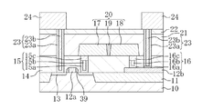
本実施形態の半導体装置では、図1に示すように、P型の半導体基板10の一部に、深さ約300nmの素子分離領域11が形成されている。そして、半導体基板10のうち素子分離領域11に囲まれる領域の上の一部には、膜厚約200nmの多結晶シリコン(Si)からなるMOSトランジスタ用のゲート電極12aと、ゲート電極12aの側壁に設けられた酸化シリコン(SiO2)からなるサイドウォール絶縁膜39とが選択的に形成されている。そして、半導体基板10のうちゲート電極12aおよびサイドウォール絶縁膜39の外側に位置する領域には、複数の拡散層13が形成されている。
In the semiconductor device of this embodiment, as shown in FIG. 1, an
一方、素子分離領域11の上には、多結晶シリコンからなる第1の配線12bが形成されている。半導体基板10、素子分離領域11、ゲート電極12a、第1の配線12b、サイドウォール絶縁膜39および拡散層13は、第1の層間絶縁膜14により覆われている。第1の層間絶縁膜14は、酸化シリコンからなり、拡散層13の上における膜厚が約500nmとなるように平坦化されている。
On the other hand, a
第1の層間絶縁膜14には、拡散層13に接続する第1のコンタクトプラグ15および第1の配線12bに接続する第2のコンタクトプラグ16が形成されている。第1のコンタクトプラグ15および第2のコンタクトプラグ16において、深さが約100nmより下側の領域は、膜厚が約5nmのチタン(Ti)(図示せず)と膜厚が約10nmの窒化チタン(TiN)からなるバリア膜15a、16aと、タングステン(W)からなる第1の埋め込み導体膜15b、16bとにより構成されている。一方、第1のコンタクトプラグ15および第2のコンタクトプラグ16における深さ約100nmまでの領域には、窒化チタンアルミニウム(TiAlN)からなる酸素バリア膜15c、16cが配置している。
In the first
なお、第1のコンタクトプラグ15が第1の配線12bに接続され、第2のコンタクトプラグ16が拡散層13に接続されていてもよい。ここで、酸素バリア膜15c、16cは、本発明における導電性バリア膜である。
Note that the
第1の層間絶縁膜14の上に、第1のコンタクトプラグ15と電気的に接続する白金(Pt)からなる第1の電極17が形成され、第1の層間絶縁膜14の上に、第2のコンタクトプラグ16と電気的に接続する白金(Pt)からなる第2の電極18が形成されている。
A
第1の電極17および第2の電極18の膜厚は、いずれも100nm以上500nm以下であって、より好ましくは約300nmである。また、第1の電極17および第2の電極18は、10nmから300nm程度、より好ましくは約100nmの距離を置いて配置されている。また、第1の電極17および第2の電極18は、基板の上方に向かって電極の幅が小さくなるテーパー形状であることが好ましい。この場合には、第1の電極17と第2の電極18との間の距離は、電極下部で約90nm、電極上部で約110nmとなっていることが好ましい。
The film thicknesses of the
なお、第1の電極17および第2の電極18は、白金に限られず、イリジウム、酸化イリジウム、ルテニウムまたは酸化ルテニウムを用いてもよい。
Note that the
第1の電極17と第2の電極18との間には、高さ方向の膜厚が約300nmの容量絶縁膜19が埋め込まれている。容量絶縁膜19は、ストロンチウム(Sr)、ビスマス(Bi)、タンタル(Ta)およびニオブ(Nb)を主成分とするビスマス層状ペロブスカイト型酸化物の強誘電体からなる。
A capacitive insulating
なお、容量絶縁膜19は、上述の組成を持つ強誘電体に限られず、これらの組成に鉛(Pb)、ジルコニウム(Zr)、チタン(Ti)、バリウム(Ba)およびランタン(La)を加えた群から選ばれた酸化物からなる強誘電体を用いてもよい。さらには、容量絶縁膜19は、強誘電体に限られず、酸化タンタル(Ta2O5)等の高誘電体を用いてもよい。
The
以上のように、第1の電極17、第2の電極18および容量絶縁膜19により、キャパシタ20を構成している。通常、複数のキャパシタ20が基板上に一度に形成されるが、これらのキャパシタ20は必ずしも同一の形状を有していなくてもよい。
As described above, the
第1の層間絶縁膜14、第1の電極17、第2の電極18および容量絶縁膜19は、第1の電極17および第2の電極18の上における膜厚が約300nmとなるように平坦化された酸化シリコンからなる第2の層間絶縁膜21により覆われている。さらに、第2の層間絶縁膜21の上には、膜厚約100nmの窒化シリコン(SiN)からなる水素バリア膜22が形成されている。
The first
第1の層間絶縁膜14、第2の層間絶縁膜21および水素バリア膜22を貫通し、第1の配線12bおよび拡散層13と接続する第3のコンタクトプラグ23が設けられている。第3のコンタクトプラグ23は、下層から、膜厚が約5nmのチタンアルミニウム(TiAl)(図示せず)と、膜厚が約10nmの窒化チタンアルミニウムからなるコンタクト水素バリア膜23aと、タングステンからなる第2の埋め込み導体膜23bが積層されたものである。
A
水素バリア膜22および第3のコンタクトプラグ23の上には、下層から、膜厚が約5nmのチタン(図示せず)と、膜厚が約50nmの窒化チタン(図示せず)と、膜厚が約500nmのアルミニウム(Al)(図示せず)と、膜厚が約30nmの窒化チタン(TiN)(図示せず)とが積層された配線24が選択的に形成されている。配線24は第3のコンタクトプラグ23を介して第1の配線12bおよび拡散層13と電気的に接続されている。
On the
水素バリア膜22および配線24の上には、図示はしていないが、他の層間絶縁膜、コンタクトおよび配線からなる多層配線や、保護膜、パッド等が形成されている。
On the
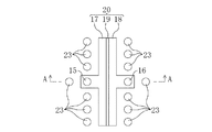
図2は本発明の第1の実施形態に係る半導体装置の構造を示す平面図である。なお、分かりやすくするため、図2では、図1の断面図にて示した構成部材の一部を省略している。 FIG. 2 is a plan view showing the structure of the semiconductor device according to the first embodiment of the present invention. For ease of understanding, some of the constituent members shown in the cross-sectional view of FIG. 1 are omitted in FIG.
図2に示すように、本実施形態の半導体装置では、第1のコンタクトプラグ15に接続された第1の電極17、第2のコンタクトプラグ16に接続された第2の電極18および第1のコンタクトプラグ15と第2のコンタクトプラグ16との間にある容量絶縁膜19によりキャパシタ20が構成されている。キャパシタ20の周辺には、第3のコンタクトプラグ23が複数個配置されている。
As shown in FIG. 2, in the semiconductor device of this embodiment, the
(変形例)
本実施形態における半導体装置の変形例を以下に説明する。図3は、第1の実施形態における半導体装置の第1の変形例を示す平面図である。図3に示すように、本実施形態の半導体装置では、第1のコンタクトプラグ15と第2のコンタクトプラグ16が、キャパシタ20の容量部に対して、対角に配置されている。つまり、第1のコンタクトプラグ15と第2のコンタクトプラグ16とを結ぶ直線と、第1の電極17と第2の電極18とが対向する面とが直交しないように配置されている。
(Modification)
A modification of the semiconductor device in this embodiment will be described below. FIG. 3 is a plan view showing a first modification of the semiconductor device according to the first embodiment. As shown in FIG. 3, in the semiconductor device of this embodiment, the
なお、第1のコンタクトプラグ15及び第2のコンタクトプラグ16は、第1の電極17及び第2の電極18に対して、どこの位置に設けられていてもよい。
Note that the
図4は、第1の実施形態における半導体装置の第2の変形例を示す平面図である。図4に示すように、1個の第1の電極17と複数の第2の電極18とから複数のキャパシタ20が構成されていてもよい。もちろん、複数の第1の電極17と1個の第2の電極18により複数のキャパシタが構成されていてもよい。
FIG. 4 is a plan view showing a second modification of the semiconductor device according to the first embodiment. As shown in FIG. 4, a plurality of
また、第1の電極17の側面のうち第2の電極18と対向する側面と反対側の側面が、他のキャパシタにおける電極として機能してもよい。つまり、第1の電極17のうち第2の電極と対向する側面と反対側の側面に、容量絶縁膜(図示せず)と電極とが設けられていてもよい。同様に、第2の電極18の側面のうち第1の電極17と対向する側面と反対側の側面が、他のキャパシタにおける電極として機能してもよい。
Moreover, the side surface opposite to the side surface facing the
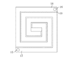
図5は、第1の実施形態における半導体装置の第3の変形例を示す平面図である。図5に示すように、第1の電極17と第2の電極18とが渦巻き状に形成されていてもよい。図6は、第1の実施形態における半導体装置の第4の変形例を示す平面図である。図6に示すように第1の電極17と第2の電極18とがくし型に形成されていてもよい。図7は、第1の実施形態における半導体装置の第5の変形例を示す平面図である。図7に示すように、第1の電極17における複数の側面を囲むように第2の電極18が形成されていてもよい。以上のような変形例によれば、面積をさほど増大させることなく、容量部の面積を増加させることができる。
FIG. 5 is a plan view showing a third modification of the semiconductor device according to the first embodiment. As shown in FIG. 5, the
本実施形態では、第1の電極17の側面部、第2の電極18の側面部および容量絶縁膜19によりキャパシタが構成されている。すなわち、半導体基板10と垂直方向に容量部が形成されているため、従来のように半導体基板に平行方向に容量部が形成されている場合と比較して、狭い領域にキャパシタを形成することができる。つまり、容量部に寄与する電極の面積を基板に垂直な方向に伸ばすことができるため、基板に平行な方向に面積を拡大することなく、容量を拡大することができる。
In the present embodiment, a capacitor is constituted by the side surface portion of the
また、第1の電極17および第2の電極18を第1のコンタクトプラグ15および第2のコンタクトプラグ16から第1の層間絶縁膜14の上まで延伸させることにより、第1のコンタクトプラグ15および第2のコンタクトプラグ16が占める領域とキャパシタ20が占める領域を分離することができる。これにより、複数個の第3のコンタクトプラグ23を含むロジックのレイアウトにおいて空いた領域の有効利用が図れる。
Further, the
また、第1の電極17および第2の電極18がテーパー形状に形成されていることにより第1の電極17の側面部と第2の電極18の側面部の間に容量絶縁膜19を形成することが容易となる。
Further, since the
また、第1の電極17あるいは第2の電極18の両側の側面部を利用してキャパシタ20の容量部を形成することにより、容量部の面積をより多く確保することができ、信頼性の高いキャパシタが得られる。容量部の面積をより多く確保する方法としては、第1の電極17および第2の電極18が、上方から見て渦巻き形状に形成したり、くし型形状に形成したりすることできる。このようにすると、小さな領域において大きな容量を確保することができる。
Further, by forming the capacitor portion of the
また、ロジック部に複数個接続されているキャパシタ20は、図8に示すように、同一形状ではなく複数種類の形状を有していることが好ましい。図8は、第1の実施形態において、ロジック部にキャパシタが複数個接続されている形態を示す平面図である。図8に示すような構成では、レイアウトの自由度が高まるとともに、必要に応じた電荷を有する容量を設計することができる。
Moreover, as shown in FIG. 8, it is preferable that the plurality of
(製造方法)
次に、第1の実施形態における半導体装置の製造方法について図面を参照しながら説明する。図9(a)〜(d)および図10(a)〜(d)は本発明の第1の実施形態に係る半導体装置の製造工程を示す断面図である。
(Production method)
Next, a method for manufacturing a semiconductor device according to the first embodiment will be described with reference to the drawings. FIGS. 9A to 9D and FIGS. 10A to 10D are cross-sectional views illustrating manufacturing steps of the semiconductor device according to the first embodiment of the present invention.
[MOSトランジスタ形成]
本実施形態の製造方法では、まず図9(a)に示す工程で、リソグラフィ法およびドライエッチング法により、シリコンからなる例えばP型の半導体基板10の上部に深さが約300nmの溝部40を形成する。続いて、CVD法により、半導体基板10の上に酸化シリコンを堆積し、化学機械的研磨(CMP)法により堆積した酸化シリコンに対して平坦化を行なって溝部40にシリコン酸化膜を埋め込む。これにより、素子分離領域11を選択的に形成する。その後、例えば熱酸化法により、半導体基板10の主面上に膜厚が約10nmのゲート絶縁膜(図示せず)を形成し、続いて、低圧CVD法により、ゲート絶縁膜の上に、膜厚が約200nmのポリシリコン(図示せず)を堆積する。その後、堆積したポリシリコンに対してリソグラフィ法およびドライエッチング法によるパターニングを行なって、ポリシリコンからなるゲート電極12aおよび第1の配線12bを形成する。続いて、CVD法により、半導体基板10の上にゲート電極12aおよび第1の配線12bを覆うように膜厚が約50nmの酸化シリコン(図示せず)を堆積し、エッチバックを行なってサイドウォール絶縁膜39を形成する。続いて、ゲート電極12a、第1の配線12bおよびサイドウォール絶縁膜39をマスクとして半導体基板10に対してイオン注入を行うことにより、MOSトランジスタ用および配線用の拡散層13を選択的に形成する。
[MOS transistor formation]
In the manufacturing method of the present embodiment, first, in the step shown in FIG. 9A, a
[電極プラグ形成]
次に、図9(b)に示す工程で、CVD法により、素子分離領域11、ゲート電極12a、第1の配線12bおよび拡散層13の上全体に亘って酸化シリコン(図示せず)を堆積した後、CMP法により、堆積した酸化シリコンに対して平坦化処理を行う。これにより、ゲート電極12aの上側における膜厚が約300nmとなる、酸化シリコンからなる第1の層間絶縁膜14を形成する。続いて、リソグラフィ法およびドライエッチング法により、第1の層間絶縁膜14のうちゲート電極12a、第1の配線12bおよび拡散層13の上に位置する部分にコンタクトホール41、42を形成する。その後、CVD法またはスパッタ法により、膜厚が約5nmのチタン(図示せず)、膜厚が約10nmの窒化チタン(図示せず)および膜厚が約200nmのタングステン(図示せず)を順次コンタクトホール41、42に充填する。続いて、エッチバック法により、コンタクトホール41、42内の上側部分を深さ約100nmまで除去することにより、バリア膜15aおよび16aと、第1の埋め込み導体膜15bおよび16bとを形成する。ここで、バリア膜15a、16aは、チタン及び窒化チタンであり、第1の埋め込み導体膜15b、16bはタングステンである。続いて、CVD法またはスパッタ法により、窒化チタンアルミニウムを約200nmの厚さでコンタクトホール41、42内の上側部分に堆積する。ここで、窒化チタンアルミニウムは酸素バリア15c、16cである。以上の工程により、酸素バリア15c、第1の埋め込み導体膜15bおよびバリア膜15aからなる第1のコンタクトプラグ15と、酸素バリア16c、第1の埋め込み導体膜16bおよびバリア膜16aからなる第2のコンタクトプラグ16とを形成する。
[Electrode plug formation]
Next, in the step shown in FIG. 9B, silicon oxide (not shown) is deposited over the
[電極形成]
次に、図9(c)に示す工程で、スパッタ法により、第1の層間絶縁膜14、第1のコンタクトプラグ15および第2のコンタクトプラグ16の上に、膜厚が約300nmの白金からなる電極膜17aおよび膜厚が約100nmの窒化チタンからなる第1のマスク材料(図示せず)を堆積する。続いて、リソグラフィ法を行うことにより、第1のマスク材料のうち第1のコンタクトプラグ15および第2のコンタクトプラグ16の上方に位置する部分を覆う第1のパターン25aを形成した後、第1のパターン25aを用いて第1のマスク材料に対してドライエッチング法を行うことにより、窒化チタンからなる第2のパターン25bを形成する。
[Electrode formation]
Next, in the step shown in FIG. 9 (c), platinum having a thickness of about 300 nm is formed on the first
次に、図9(d)に示す工程で、アッシング法により、第1のパターン25aを除去する。その後、CVD法またはスパッタ法により、膜厚が約100nmの窒化チタンを堆積し、続いて、エッチバック法により、第2のパターン25bの側壁に第3のパターン25cを形成する。
Next, in the step shown in FIG. 9D, the
次に、図10(a)に示す工程で、第2のパターン25bおよび第3のパターン25cをマスクとして電極膜17aに対してエッチングを行うことにより、第1のコンタクトプラグ15を含む領域の上方に第1の電極17を、第2のコンタクトプラグ16を含む領域の上に第2の電極18を形成する。
Next, in the step shown in FIG. 10A, the
[容量絶縁膜形成]
次に、図10(b)に示す工程で、有機金属気相堆積(MOCVD)法により、第1の電極17と第2の電極18との間を含む第1の層間絶縁膜14、第1の電極17および第2の電極18の上に、約100nmの膜厚を有し、ストロンチウム、ビスマス、タンタル又はニオブを主成分とするビスマス層状ペロブスカイト型酸化物である強誘電体膜(図示せず)を堆積する。続いて、エッチバック法により強誘電体を約50nmまで除去するエッチングを行い、エッチバックされた強誘電体膜19aを形成する。
[Capacitance insulation film formation]
Next, in the step shown in FIG. 10B, the first
次に、図10(c)に示す工程で、強誘電体膜19aの上に約100nmの強誘電体膜(図示せず)を堆積する。続いて、エッチバック法により、強誘電体膜19aおよび強誘電体膜(図示せず)のうち第1の電極17と第2の電極18との間に介在する部分を残してそれ以外の部分を除去することにより、第1の層間絶縁膜14を露出させると共に第1の電極17と第2の電極18との間に容量絶縁膜19を形成する。このようにして、第1の電極17、第2の電極18および容量絶縁膜19からなるキャパシタ20を形成する。
Next, in the step shown in FIG. 10C, a ferroelectric film (not shown) of about 100 nm is deposited on the
[水素バリアおよび配線形成]
次に、図10(d)に示す工程で、CVD法により、第1の層間絶縁膜14、第1の電極17および第2の電極18を含む全面の上にわたって酸化シリコンを堆積した後、CMP法により、堆積した酸化シリコンに対して第1の電極17および第2の電極18の上側部分の膜厚が約300nmとなるように平坦化して、酸化シリコンからなる第2の層間絶縁膜21を形成する。
[Hydrogen barrier and wiring formation]
Next, in the step shown in FIG. 10D, after depositing silicon oxide over the entire surface including the first
続いて、CVD法により、膜厚約100nmの窒化シリコンからなる水素バリア膜22を形成した後、リソグラフィ法およびドライエッチング法により、第1の層間絶縁膜14、第2の層間絶縁膜21および水素バリア膜22を貫通し、ゲート電極12a、第1の配線12bおよび拡散層13に到達するコンタクトホール43、44を形成する。
Subsequently, after a
その後、CVD法またはスパッタ法により、水素バリア膜22の上に、膜厚が約5nmのチタンアルミニウム(図示せず)、膜厚が約10nmの窒化チタンアルミニウム(図示せず)および膜厚が約200nmのタングステン(図示せず)を順次コンタクトホール43、44に充填されるように堆積する。続いて、CMP法により堆積膜において第2の層間絶縁膜21上に残る部分を除去し、チタンアルミニウムと窒化チタンアルミニウムからなるコンタクト水素バリア膜23aと、タングステンからなる第2の埋め込み導体膜23bとから構成される第3のコンタクトプラグ23を形成する。
Thereafter, a titanium aluminum (not shown) having a thickness of about 5 nm, a titanium aluminum nitride (not shown) having a thickness of about 10 nm, and a thickness of about 10 nm are formed on the
続いて、スパッタ法により、水素バリア膜22の上に、第3のコンタクトプラグ23と接するように、膜厚が約5nmのチタン(図示せず)、膜厚が約50nmの窒化チタン(図示せず)、膜厚が約500nmのアルムミニウム(図示せず)および膜厚が約30nmの窒化チタン(図示せず)を順次堆積する。その後、堆積した積層膜に対してドライエッチング法によるパターニングを行なって、積層膜から配線24を形成する。
Subsequently, by sputtering, titanium (not shown) having a thickness of about 5 nm and titanium nitride (not shown) having a thickness of about 50 nm are formed on the
次に、図示はしていないが、多層配線の形成、保護膜の形成、およびパッドの形成等の公知の製造プロセスを行うことにより、本実施形態の半導体装置を得ることができる。 Next, although not shown, the semiconductor device of this embodiment can be obtained by performing known manufacturing processes such as formation of multilayer wiring, formation of a protective film, and formation of pads.
本実施形態の製造方法によると、第1の電極17と第2の電極18を同時に形成するため、従来のように別々にパターン形成する場合に比べ、マスク工程を削減できる。これにより、コストの低減および製造時間の短時間化が可能となる。
According to the manufacturing method of the present embodiment, since the
また、第2のパターン25bの側壁に第3のパターン25cを形成するため、第1の電極17と第2の電極18との距離を、レジストで形成できるパターン間の最小の距離よりも小さくすることができる。
Further, in order to form the
また、本実施形態では、容量絶縁膜19を形成する工程が、容量絶縁膜の成膜工程とエッチバック工程から構成される。これにより、マスク工程を削減でき、コストの低減および製造時間の短時間化が可能となる。また、容量絶縁膜の成膜とエッチバックとを複数回繰り返すことにより、第1の電極17と第2の電極18との間への容量絶縁膜19の埋め込み特性を改善し、キャパシタの信頼性および歩留まりを高めることができる。
In the present embodiment, the process of forming the capacitive insulating
(第2の実施形態)
以下に、本発明の第2の実施形態について図面を参照しながら説明する。本実施形態の製造方法は、第1の実施形態の製造方法における[容量絶縁膜形成]の方法を変更したものである。
(Second Embodiment)
Below, the 2nd Embodiment of this invention is described, referring drawings. The manufacturing method of the present embodiment is a modification of the [capacitor insulating film formation] method in the manufacturing method of the first embodiment.
図11(a)〜(d)は、本発明の第2の実施形態に係る半導体装置の製造工程を示す断面図である。図11(a)〜(d)において、図9(a)〜(d)および図10(a)〜(d)に示す構成部材と同一の構成部材には同一の符号を付してその説明を省略する。 11A to 11D are cross-sectional views illustrating the manufacturing steps of the semiconductor device according to the second embodiment of the present invention. In FIGS. 11A to 11D, the same components as those shown in FIGS. 9A to 9D and FIGS. Is omitted.
[容量絶縁膜形成]
本実施形態における容量絶縁膜の製造方法では、図10(a)に示す工程と同様の方法により第1の電極17および第2の電極18を形成した後、図11(a)に示す工程で、オクタンからなる粘度の小さい第1の溶液26aを塗布する。第1の溶液26aの厚さは、第1の電極17および第2の電極18が浸漬するように、300nmから1000nm程度、より好ましくは約500nmとする。
[Capacitance insulation film formation]
In the method of manufacturing the capacitive insulating film in this embodiment, after the
次に、図11(b)に示す工程で、半導体基板10を回転させることにより、第1の溶液26aの大部分を除去し、主として第1の電極17と第2の電極18との間に第1の溶液26bを残存させる。
Next, in the step shown in FIG. 11B, the
次に、図11(c)に示す工程で、第1の溶液26bに比べ粘度が大きくかつ強誘電体を構成する金属元素を含んでいる第2の溶液27aを塗布する。第2の溶液27aの厚さは300nmから4000nm程度、より好ましくは約2000nmとする。
Next, in the step shown in FIG. 11C, a second solution 27a having a viscosity higher than that of the
次に、図11(d)に示す工程で、半導体基板10を揺動することにより、第1の溶液26bと第2の溶液27aとを混合する。これにより、第2の溶液27aよりも強誘電体を構成する金属元素の濃度の低い混合溶液を得る。続いて、半導体基板10を回転させることにより、第1の層間絶縁膜14の上における第1の溶液26bと第2の溶液27aとの混合液を薄膜化した後、酸素(O2)雰囲気下でRTA(急速加熱処理)法により強誘電体を結晶化させる。RTA法の温度は600℃から800℃程度、より好ましくは700℃とする。また、RTA法の時間は30秒から10分程度、より好ましくは1分程度とする。続いて、エッチバック法により、強誘電体膜のうち第1の電極17と第2の電極18との間に位置する部分以外が除去されるようにエッチングを行うことにより、強誘電体からなる容量絶縁膜27を形成する。
Next, in the step shown in FIG. 11D, the
本実施形態の製造方法によると、第1の電極17および第2の電極18との間に、まず粘度の小さい第1の溶液26aを挿入することができる。その後、第1の溶液26aを第2の溶液27aと接触させた状態で振動を与える。これにより、第1の溶液26bと第2の溶液27aとを混合させる。従って、比較的粘度が高く、第1の電極17および第2の電極18との間に入り込みにくい第2の溶液27aを第1の電極17および第2の電極1との8間に挿入することができる。このような方法により、第1の電極17と第2の電極18との間の距離が小さい場合でも容量絶縁膜19を形成することができる。
According to the manufacturing method of the present embodiment, the
(第3の実施形態)
以下に、本発明の第3の実施形態について図面を参照しながら説明する。図12は、本発明の第3の実施形態に係る半導体装置の構造を示す断面図である。図12において、図1に示す構成部材と同一の構成部材には同一の符号を付してその説明を省略する。
(Third embodiment)
The third embodiment of the present invention will be described below with reference to the drawings. FIG. 12 is a cross-sectional view showing the structure of a semiconductor device according to the third embodiment of the present invention. In FIG. 12, the same components as those shown in FIG. 1 are denoted by the same reference numerals, and the description thereof is omitted.
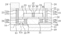
本実施形態は、コンタクトプラグを形成するコンタクトホールの上部に酸素バリアが埋め込まれていた第1の実施形態と異なり、コンタクトプラグの上に酸素バリアを設けた点に特徴をもつ。 This embodiment is characterized in that an oxygen barrier is provided on the contact plug, unlike the first embodiment in which an oxygen barrier is buried in the upper part of the contact hole forming the contact plug.
本実施形態の半導体装置では、図12に示すように、第1の層間絶縁膜14には、拡散層13および第1の配線12bにそれぞれ接続する第1のコンタクトプラグ28および第2のコンタクトプラグ29が形成されている。第1のコンタクトプラグ28および第2のコンタクトプラグ29は、下から順に形成された膜厚が約5nmのチタン(Ti)(図示せず)と、膜厚が約10nmの窒化チタン(TiN)からなる積層のバリア膜28a、29aと、バリア膜28a、29aの上に形成されたタングステン(W)からなる第1の埋め込み導体膜28b、29bから構成される。第1のコンタクトプラグ28および第2のコンタクトプラグ29は、拡散層13および第1の配線12bのいずれに接続されていてもよい。
In the semiconductor device of the present embodiment, as shown in FIG. 12, the first
第1のコンタクトプラグ28および第2のコンタクトプラグ29の上を覆う部分には、第1の酸素バリア30および第2の酸素バリア31が形成されている。第1の酸素バリア30および第2の酸素バリア31は、下から順次形成された窒化チタンアルミニウム、イリジウム、及び酸化イリジウムとからなる積層膜である。ここで、窒化チタンアルミニウムの膜厚は10nmから200nm程度であり、より好ましくは約50nmである。また、イリジウムの膜厚は10nmから200nm程度であり、より好ましくは約50nmである。さらに、酸化イリジウムの膜厚は10nmから200nm程度であり、より好ましくは約50nmである。第1の酸素バリア30および第2の酸素バリア31は、第1のコンタクトプラグ28および第2のコンタクトプラグ29を覆っている。
A
一方、第1の層間絶縁膜14の上のうち第1の酸素バリア30と第2の酸素バリア31が形成されていない領域は、酸化シリコンからなる埋め込み絶縁膜32により覆われている。
On the other hand, a region on the first
そして、第1の酸素バリア30、第2の酸素バリア31および埋め込み絶縁膜32の上には、第1の実施形態に係る半導体装置と同様に、キャパシタ20、第2の層間絶縁膜21、水素バリア膜22、第3のコンタクトプラグ23、配線24等が形成されている。
Then, on the
本実施形態の半導体装置によると、第1のプラグおよび第2のプラグの上に第1の酸素バリア30および第2の酸素バリア31を形成するため、酸素雰囲気下において高温で強誘電体を成膜しても、プラグの酸化が起こらない。そのため、プラグの歩留まりを高めることができる。 本発明における第2の半導体装置の製造方法によると、第1の電極と第2の電極とを同時に形成することができるため、マスク工程を削減することができる。さらに、導電性バリア膜によりプラグの酸化を防ぐことができる。また、酸素バリアの側面を埋め込んでいるため、その上に第1の電極および第2の電極を形成するためのリソグラフィーにおけるフォーカスマージンを確保でき、キャパシタの歩留まりを高めることができる。
According to the semiconductor device of this embodiment, since the
なお、本実施形態では、第1の酸素バリア30および第2の酸素バリア31として、窒化チタンアルミニウム、イリジウムおよび酸化イリジウムの積層膜を用いた。しかしながら、本発明の第1の酸素バリア30および第2の酸素バリア31はこれには限定されず、例えばルテニウム、酸化ルテニウム、チタンアルミニウム、珪化窒化チタン、窒化タンタル、珪化窒化タンタル、窒化タンタルアルミニウムまたはタンタルアルミニウム等により構成されていてもよい。
In the present embodiment, a stacked film of titanium aluminum nitride, iridium, and iridium oxide is used as the
(製造方法)
次に、第3の実施形態における半導体装置の製造方法について図面を参照しながら説明する。本実施形態の製造方法は、第1の実施形態の製造方法における[電極プラグ形成]の方法を変更したものである。
(Production method)
Next, a semiconductor device manufacturing method according to the third embodiment will be described with reference to the drawings. The manufacturing method of this embodiment is a modification of the [electrode plug formation] method in the manufacturing method of the first embodiment.
図13(a)〜(d)は、本発明の第3の実施形態に係る半導体装置の製造方法を示す断面図である。図13(a)〜(c)において、図9(a)〜(d)および図10(a)〜(d)に示す構成部材と同一の構成部材には同一の符号を付してその説明を省略する。 13A to 13D are cross-sectional views illustrating a method for manufacturing a semiconductor device according to the third embodiment of the present invention. 13 (a) to (c), the same components as those shown in FIGS. 9 (a) to 9 (d) and FIGS. Is omitted.
[電極プラグ形成]
本実施形態における電極プラグの製造方法では、図9(a)と同様に、半導体基板10の上に素子分離領域11、ゲート電極12a、第1の配線12bおよび拡散層13を形成した後、図13(a)に示すように、CVD法により、素子分離領域11、ゲート電極12a、第1の配線12bおよび拡散層13の上全体にわたって酸化シリコン(図示せず)を堆積した後、CMP法により、堆積した酸化シリコンに対してゲート電極12aの上側部分の膜厚が約300nmとなるように平坦化を行い、酸化シリコンからなる第1の層間絶縁膜14を形成する。
[Electrode plug formation]
In the electrode plug manufacturing method according to the present embodiment, after the
続いて、リソグラフィ法およびドライエッチング法により、第1の層間絶縁膜14における第1の配線12bおよび拡散層13の上側部分にコンタクトホール44、45を形成する。その後、CVD法またはスパッタ法により、膜厚が約5nmのチタン、膜厚が約10nmの窒化チタンおよび膜厚が約200nmのタングステンを下から順次コンタクトホールに充填して積層膜を形成し、続いて、CMP法により堆積膜のうち第1の層間絶縁膜14の上に残る部分を除去することにより、バリア膜28aおよび第1の埋め込み導体膜28bからなる第1のコンタクトプラグ28と、バリア膜29aおよび第1の埋め込み導体膜29bからなる第2のコンタクトプラグ29とを形成する。
Subsequently, contact holes 44 and 45 are formed in the upper portion of the
次に、図13(b)に示すように、第1の層間絶縁膜14の上に、スパッタ法により、膜厚が約50nmの窒化チタンアルミニウム(図示せず)、膜厚が約50nmのイリジウム(図示せず)および膜厚が約50nmの酸化イリジウム(図示せず)を下から順次堆積する。その後、リソグラフィ法およびドライエッチング法によって選択的にパターニングを行うことにより、第1のコンタクトプラグ28の上を覆う第1の酸素バリア30と、第2のコンタクトプラグ29の上を覆う第2の酸素バリア31とを形成する。
Next, as shown in FIG. 13B, titanium aluminum nitride (not shown) having a thickness of about 50 nm and iridium having a thickness of about 50 nm are formed on the first
次に、図13(c)に示すように、CVD法により、第1の層間絶縁膜14、第1の酸素バリア30および第2の酸素バリア31の上全体にわたって酸化シリコンを堆積した後、CMP法若しくはエッチバック法又はその組み合わせにより、堆積した酸化シリコンに対して平坦化を行う。これにより、第1の酸素バリア30および第2の酸素バリア31の表面を露出して、酸化シリコンからなる埋め込み絶縁膜32を形成する。
Next, as shown in FIG. 13C, after depositing silicon oxide over the first
その後、図示しないが、第1の酸素バリア30、第2の酸素バリア31、および埋め込み絶縁膜32上に、第1の実施形態に係る半導体装置の製造方法と同様に、キャパシタ20、第3のコンタクトプラグ23、配線24等を形成する。
Thereafter, although not shown, the
本実施形態の製造方法によると、第1の酸素バリア30および第2の酸素バリア31によりプラグの酸化を防ぐことができる。また、酸素バリアの側面を埋め込んでいるため、第1の電極と第2の電極のパターン形成時において、リソグラフィーのフォーカスマージンを確保することができる。これにより、キャパシタの歩留まりを高めることができる。
According to the manufacturing method of the present embodiment, the
(第4の実施形態)
以下に、本発明の第4の実施形態について図面を参照しながら説明する。図14は、本発明の第4の実施形態に係る半導体装置の構造を示す断面図である。図14において、図12に示す構成部材と同一の構成部材には同一の符号を付してその説明を省略する。
(Fourth embodiment)
The fourth embodiment of the present invention will be described below with reference to the drawings. FIG. 14 is a sectional view showing a structure of a semiconductor device according to the fourth embodiment of the present invention. In FIG. 14, the same components as those shown in FIG. 12 are denoted by the same reference numerals, and the description thereof is omitted.
本実施形態の半導体装置では、図14に示すように、第1の酸素バリア30の一部の上からその周囲における埋め込み絶縁膜32の上に亘って、膜厚が100nmから500nm程度、より好ましくは約300nm程度の第1のパターン絶縁膜33が形成されている。そして、該第1のパターン絶縁膜33の側壁には、白金からなる第1の電極35が形成されている。第1の電極35の一部は、第1の酸素バリア30に接している。
In the semiconductor device of the present embodiment, as shown in FIG. 14, the film thickness is preferably about 100 nm to 500 nm from a part of the
同様に、第2の酸素バリア31の一部の上からその周囲における埋め込み絶縁膜32の上に亘って、膜厚が100nmから500nm程度、より好ましくは約300nm程度の第2のパターン形成膜34が形成されている。そして、該第2のパターン絶縁膜34の側壁には、白金からなる第2の電極36が形成されている。第2の電極36の一部は、第2の酸素バリア31に接している。なお、第1のパターン絶縁膜33および第2のパターン絶縁膜34の材質は酸化シリコンに限られず、窒化シリコン、または酸化窒化シリコン等であってもよい。また、第1の電極35および第2の電極36の材質は白金に限られず、イリジウム、酸化イリジウム、ルテニウム、酸化ルテニウム等であってもよい。
Similarly, the second
埋め込み絶縁膜32、第1のパターン絶縁膜33、第2のパターン絶縁膜34、第1の電極35および第2の電極36の上には、第3の実施形態に係る半導体装置と同様に、容量絶縁膜19、第2の層間絶縁膜21、水素バリア膜22、第3のコンタクトプラグ23、配線24等が形成されている。
On the buried insulating
図15は本発明の第4の実施形態に係る半導体装置の構成を示す平面図である。なお、分かりやすくするため、図14の断面構成にて示した構成部材の一部は省略している。図15に示すように、本実施形態の半導体装置では、第1の酸素バリア30に接続された第1の電極35、第2の酸素バリア31に接続された第2の電極36および第1の電極35と第2の電極36との間にある容量絶縁膜19によってキャパシタ37が構成されている。該キャパシタ37周辺には、第3のコンタクトプラグ23が複数個配置されている。なお、キャパシタ37は複数個配置されていてもよい。なお、図14は、図15におけるA−A線に沿った断面構造を示している。
FIG. 15 is a plan view showing a configuration of a semiconductor device according to the fourth embodiment of the present invention. For ease of understanding, some of the constituent members shown in the cross-sectional configuration of FIG. 14 are omitted. As shown in FIG. 15, in the semiconductor device of this embodiment, the
本実施形態では、エッチングが困難な材料である白金をパターン絶縁膜の側壁にのみ形成すればよいため、パターン形成が容易となる。 In this embodiment, platinum, which is a material that is difficult to etch, may be formed only on the side wall of the pattern insulating film, so that pattern formation is facilitated.
(製造方法)
次に、第4の実施形態における半導体装置の製造方法について図面を参照しながら説明する。第4の実施形態は、第3の実施形態における製造方法の[電極形成]の方法を変更したものである。
(Production method)
Next, a method for manufacturing a semiconductor device according to the fourth embodiment will be described with reference to the drawings. In the fourth embodiment, the [electrode formation] method of the manufacturing method in the third embodiment is changed.
図16(a)、(b)は、本発明の第4の実施形態に係る半導体装置の製造工程を示す断面図である。図16(a)、(b)において、図9(a)〜(d)、図10(a)〜(d)、および図13(a)〜(c)に示す構成部材と同一の構成部材には同一の符号を付すことにより説明を省略する。 16A and 16B are cross-sectional views illustrating the manufacturing steps of the semiconductor device according to the fourth embodiment of the present invention. 16 (a) and 16 (b), the same components as those shown in FIGS. 9 (a) to 9 (d), FIGS. 10 (a) to (d), and FIGS. 13 (a) to 13 (c). The description will be omitted by attaching the same reference numerals to.
[電極形成]
本実施形態の製造方法では、図13(c)に示す工程で、第1の酸素バリア30および第2の酸素バリア31の表面を露出した埋め込み絶縁膜32を形成した後、図16(a)に示す工程で、CVD法により、膜厚が約300nmの酸化シリコンを形成する。続いて、リソグラフィ法およびドライエッチング法により選択的なパターニングを行い、第1の酸素バリア30の一部の上からその周囲における埋め込み絶縁膜32の上を覆う第1のパターン形成膜33と、第2の酸素バリア31の一部の上からその周囲における埋め込み絶縁膜32の上を覆う第2のパターン形成膜34とを形成する。
[Electrode formation]
In the manufacturing method of this embodiment, after the buried insulating
次に、図16(b)に示す工程で、CVD法またはスパッタ法により、第1の酸素バリア30、第2の酸素バリア31、埋め込み絶縁膜32、第1のパターン絶縁膜33および第2のパターン絶縁膜34の上全体にわたって、膜厚が約100nmの白金(図示せず)を堆積する。その後、エッチバック法により、第1のパターン絶縁膜33側壁に白金からなる第1の電極35を形成し、第2のパターン絶縁膜34側壁に白金からなる第2の電極36を形成する。ここで、本発明の第1の電極は、第1のパターン絶縁膜33と第1の電極35とからなり、本発明の第2の電極は、第2のパターン絶縁膜34と第2の電極36とからなる。ただし、第1のパターン絶縁膜33の側壁に形成された第1の電極35が本発明の第1の導電膜であり、第2の電極36が本発明の第2の導電膜としてもよいのは言うまでもない。
Next, in the step shown in FIG. 16B, the
本実施形態では、エッチングが困難な材料である白金をパターン絶縁膜の側壁にのみ形成すればよいため、パターン形成が容易となる。 In this embodiment, platinum, which is a material that is difficult to etch, may be formed only on the side wall of the pattern insulating film, so that pattern formation is facilitated.
本発明に係る半導体装置は、キャパシタのレイアウトの自由度を高め、ロジック部の空いた領域の有効利用を図るのに有用である。 The semiconductor device according to the present invention is useful for increasing the degree of freedom of the capacitor layout and effectively utilizing the area where the logic portion is free.
10 半導体基板
11 素子分離領域
12a ゲート電極
12b 第1の配線
13 拡散層
14 第1の層間絶縁膜
15 第1のコンタクトプラグ
15a、16a バリア膜
15b、16b 導体膜
15c、16c 酸素バリア
16 第2のコンタクトプラグ
17 第1の電極
17a 電極膜
18 第2の電極
19 容量絶縁膜
19a 強誘電体膜
20 キャパシタ
21 第2の層間絶縁膜
22 水素バリア膜
23 第3のコンタクトプラグ
23a コンタクト水素バリア膜
23b 導体膜
24 配線
25a 第1のパターン
25b 第2のパターン
25c 第3のパターン
26a、26b 第1の溶液
27 容量絶縁膜
27a 第2の溶液
28 第1のコンタクトプラグ
28a、29a バリア膜
28b、29b 導体膜
29 第2のコンタクトプラグ
29a バリア膜
29b 導体膜
30 第1の酸素バリア
31 第2の酸素バリア
32 絶縁膜
33 第1のパターン絶縁膜
34 第2のパターン絶縁膜
35 第1の電極
36 第2の電極
37 キャパシタ
39 サイドウォール
40 溝部
41〜45 コンタクトホール
10 Semiconductor substrate
11 Device isolation region
12a Gate electrode
12b First wiring
13 Diffusion layer
14 First interlayer insulating film
15 First contact plug
15a, 16a barrier film
15b, 16b conductor film
15c, 16c oxygen barrier
16 Second contact plug
17 First electrode
17a Electrode film
18 Second electrode
19 Capacitive insulation film
19a Ferroelectric film
20 capacitors
21 Second interlayer insulating film
22 Hydrogen barrier film
23 Third contact plug
23a Contact hydrogen barrier film
23b Conductor film
24 Wiring
25a first pattern
25b Second pattern
25c third pattern
26a, 26b first solution
27 Capacitive insulating film
27a second solution
28 First contact plug
28a, 29a Barrier film
28b, 29b Conductor film
29 Second contact plug
29a barrier film
29b Conductor film
30 First oxygen barrier
31 Second oxygen barrier
32 Insulating film
33 First pattern insulating film
34 Second pattern insulating film
35 first electrode
36 Second electrode
37 capacitors
39 sidewall
40 groove
41-45 contact hole
Claims (23)
前記絶縁膜を貫通する第1のプラグ及び第2のプラグと、
前記絶縁膜の上に形成され、前記第1のプラグと電気的に接続する第1の電極と、
前記絶縁膜の上に形成され、前記第2のプラグと電気的に接続する第2の電極と、
前記第1の電極の側面と前記第2の電極の側面とが対向する間にのみ形成された容量絶縁膜とを含み、
前記第1の電極、前記容量絶縁膜および前記第2の電極によりキャパシタが構成され、
前記第1の電極の上面、前記第2の電極の上面、及び前記容量絶縁膜の上面の高さは等しいことを特徴とする半導体装置。 An insulating film formed on the semiconductor substrate;
A first plug and a second plug penetrating the insulating film;
A first electrode formed on the insulating film and electrically connected to the first plug;
A second electrode formed on the insulating film and electrically connected to the second plug;
A capacitive insulating film formed only while the side surface of the first electrode and the side surface of the second electrode face each other;
A capacitor is constituted by the first electrode, the capacitive insulating film, and the second electrode,
The height of the upper surface of the first electrode, the upper surface of the second electrode, and the upper surface of the capacitor insulating film is the same.
前記第2のプラグと前記第2の電極との間に形成された第2の導電性バリア膜とをさらに備えることを特徴とする請求項1記載の半導体装置。 A first conductive barrier film formed between the first plug and the first electrode;
The semiconductor device according to claim 1, further comprising a second conductive barrier film formed between the second plug and the second electrode.
前記第2の電極のうち前記容量絶縁膜と接する面と、前記第2の電極における下面との成す角が鈍角であることを特徴とする請求項1または2に記載の半導体装置。 An angle formed between a surface of the first electrode that is in contact with the capacitive insulating film and a lower surface of the first electrode is an obtuse angle,
3. The semiconductor device according to claim 1, wherein an angle formed between a surface of the second electrode in contact with the capacitive insulating film and a lower surface of the second electrode is an obtuse angle.
前記第2の電極は、第2のパターン絶縁膜と、前記第2のパターン絶縁膜の側面に形成された第2の導電膜とを有し、前記第2の導電膜は前記第2のプラグと電気的に接続することを特徴とする請求項1〜6のうちのいずれか1項に記載の半導体装置。 The first electrode includes a first pattern insulating film and a first conductive film formed on a side surface of the first pattern insulating film, and the first conductive film is the first plug. Electrically connect with
The second electrode includes a second pattern insulating film and a second conductive film formed on a side surface of the second pattern insulating film, and the second conductive film is the second plug. The semiconductor device according to claim 1, wherein the semiconductor device is electrically connected to the semiconductor device.
半導体基板の上に絶縁膜を形成する工程(A)と、
前記絶縁膜を貫通する第1のプラグおよび第2のプラグを形成する工程(B)と、
前記絶縁膜の上に、前記第1のプラグと電気的に接続する前記第1の電極と、前記第2のプラグと電気的に接続する前記第2の電極とを形成する工程(C)と、
前記第1の電極と前記第2の電極とが対向する領域に前記容量絶縁膜を形成する工程(D)とを備えることを特徴とする半導体装置の製造方法。 A method of forming a capacitor comprising a first electrode, a capacitive insulating film, and a second electrode,
Forming an insulating film on the semiconductor substrate (A);
A step (B) of forming a first plug and a second plug penetrating the insulating film;
Forming the first electrode electrically connected to the first plug and the second electrode electrically connected to the second plug on the insulating film; ,
And (D) forming the capacitive insulating film in a region where the first electrode and the second electrode are opposed to each other.
前記絶縁膜上に、前記第1のプラグの上面を覆う第1の導電性バリア膜と、前記第2のプラグの上面を覆う第2の導電性バリア膜とを形成する工程をさらに備えることを特徴とする請求項13に記載の半導体装置の製造方法。 After the step (B) and before the step (C),
Forming a first conductive barrier film covering the upper surface of the first plug and a second conductive barrier film covering the upper surface of the second plug on the insulating film; 14. The method for manufacturing a semiconductor device according to claim 13, wherein the method is a semiconductor device.
前記絶縁膜上に、電極用導電膜を成膜する工程と、
前記電極用導電膜上に、前記第1のプラグ及び前記第2のプラグの上方を覆う第1のレジストパターンを形成する工程と、
前記第1のレジストパターンの側壁に第2のレジストパターンを形成する工程と、
前記第1のレジストパターンおよび前記第2のレジストパターンをマスクとして前記電極用導電膜をエッチングすることにより、前記第1の電極および前記第2の電極を形成する工程とを備えることを特徴とする請求項13または14に記載の半導体装置の製造方法。 The step (C)
Forming a conductive film for an electrode on the insulating film;
Forming a first resist pattern covering the upper portion of the first plug and the second plug on the electrode conductive film;
Forming a second resist pattern on a sidewall of the first resist pattern;
Forming the first electrode and the second electrode by etching the electrode conductive film using the first resist pattern and the second resist pattern as a mask. 15. A method for manufacturing a semiconductor device according to claim 13 or 14.
前記絶縁膜上に、前記第1のプラグの上方を覆う前記第1のパターン絶縁膜と、前記第2のプラグの上方を覆う前記第2のパターン絶縁膜とを形成する工程と、
前記第1のパターン絶縁膜および前記第2のパターン絶縁膜の上に、導電膜を形成する工程と、
エッチバックにより、前記第1のパターン絶縁膜の側壁に、前記第1のプラグと接続する前記第1の導電膜を形成し、前記第2のパターン絶縁膜の側壁に、前記第2のプラグと接続する前記第2の導電膜を形成する工程とを含み、
前記第1の電極は、前記第1のパターン絶縁膜と前記第1の導電膜とからなり、
前記第2の電極は、前記第2のパターン絶縁膜と前記第2の導電膜とからなることを特徴とする請求項13または14に記載の半導体装置の製造方法。 The step (C)
Forming the first pattern insulating film covering the upper portion of the first plug and the second pattern insulating film covering the upper portion of the second plug on the insulating film;
Forming a conductive film on the first pattern insulating film and the second pattern insulating film;
Etch-back forms the first conductive film connected to the first plug on the side wall of the first pattern insulating film, and the second plug on the side wall of the second pattern insulating film. Forming the second conductive film to be connected,
The first electrode includes the first pattern insulating film and the first conductive film,
15. The method of manufacturing a semiconductor device according to claim 13, wherein the second electrode includes the second pattern insulating film and the second conductive film.
前記容量絶縁膜を成膜する工程及び前記容量絶縁膜をエッチバックする工程を少なくとも1回行なうことを特徴とする請求項13〜16のうちのいずれか1項に記載の半導体装置の製造方法。 In the step (D),
The method for manufacturing a semiconductor device according to claim 13, wherein the step of forming the capacitor insulating film and the step of etching back the capacitor insulating film are performed at least once.
前記第1の電極と前記第2の電極との間に第1の溶液を塗布する工程と、
前記第1の溶液の上に、前記第1の溶液に比べ粘度が大きくかつ前記容量絶縁膜を構成する金属元素を含む第2の溶液を塗布する工程とを含むことを特徴とする請求項13〜17のうちのいずれか1項に記載の半導体装置の製造方法。 The step (D)
Applying a first solution between the first electrode and the second electrode;
And applying a second solution containing a metal element having a viscosity higher than that of the first solution and constituting the capacitive insulating film on the first solution. The manufacturing method of the semiconductor device of any one of -17.
Priority Applications (1)
| Application Number | Priority Date | Filing Date | Title |
|---|---|---|---|
| JP2005063884A JP2006253194A (en) | 2005-03-08 | 2005-03-08 | Semiconductor device and manufacturing method thereof |
Applications Claiming Priority (1)
| Application Number | Priority Date | Filing Date | Title |
|---|---|---|---|
| JP2005063884A JP2006253194A (en) | 2005-03-08 | 2005-03-08 | Semiconductor device and manufacturing method thereof |
Publications (2)
| Publication Number | Publication Date |
|---|---|
| JP2006253194A true JP2006253194A (en) | 2006-09-21 |
| JP2006253194A5 JP2006253194A5 (en) | 2006-12-28 |
Family
ID=37093386
Family Applications (1)
| Application Number | Title | Priority Date | Filing Date |
|---|---|---|---|
| JP2005063884A Withdrawn JP2006253194A (en) | 2005-03-08 | 2005-03-08 | Semiconductor device and manufacturing method thereof |
Country Status (1)
| Country | Link |
|---|---|
| JP (1) | JP2006253194A (en) |
Cited By (2)
| Publication number | Priority date | Publication date | Assignee | Title |
|---|---|---|---|---|
| US8367428B2 (en) | 2006-11-14 | 2013-02-05 | Fujitsu Semiconductor Limited | Semiconductor device and manufacturing method thereof |
| JP2014057104A (en) * | 2013-12-16 | 2014-03-27 | Fujitsu Semiconductor Ltd | Semiconductor device and manufacturing method of the same |
-
2005
- 2005-03-08 JP JP2005063884A patent/JP2006253194A/en not_active Withdrawn
Cited By (2)
| Publication number | Priority date | Publication date | Assignee | Title |
|---|---|---|---|---|
| US8367428B2 (en) | 2006-11-14 | 2013-02-05 | Fujitsu Semiconductor Limited | Semiconductor device and manufacturing method thereof |
| JP2014057104A (en) * | 2013-12-16 | 2014-03-27 | Fujitsu Semiconductor Ltd | Semiconductor device and manufacturing method of the same |
Similar Documents
| Publication | Publication Date | Title |
|---|---|---|
| US6737694B2 (en) | Ferroelectric memory device and method of forming the same | |
| US7208367B2 (en) | Methods of fabricating ferroelectric memory devices having expanded plate lines | |
| US20030170919A1 (en) | Ferroelectric memory device using via etch-stop layer and method for manufacturing the same | |
| US20050205912A1 (en) | Ferroelectric memory device with merged-top-plate structure and method for fabricating the same | |
| US20060183252A1 (en) | Ferroelectric memory devices | |
| JP4181135B2 (en) | Semiconductor memory device | |
| US20100052021A1 (en) | Semiconductor memory device | |
| JP2005217189A (en) | Capacitive element and its manufacturing method | |
| JP3643091B2 (en) | Semiconductor memory device and manufacturing method thereof | |
| JP3621087B1 (en) | Semiconductor device and manufacturing method thereof | |
| JP2008130615A (en) | Semiconductor memory device, and its manufacturing method | |
| JP4766924B2 (en) | Semiconductor memory device and manufacturing method thereof | |
| JP2010225928A (en) | Semiconductor memory device and manufacturing method of the same | |
| JP2007005409A (en) | Dielectric memory and its manufacturing method | |
| JP2006253194A (en) | Semiconductor device and manufacturing method thereof | |
| JP2004207681A (en) | Semiconductor device and manufacturing method therefor | |
| JP4002882B2 (en) | Capacitor element, semiconductor memory device and manufacturing method thereof | |
| JP4636834B2 (en) | Semiconductor device and manufacturing method thereof | |
| JP4509992B2 (en) | Semiconductor device and manufacturing method thereof | |
| JP2007035915A (en) | Semiconductor device and its manufacturing method | |
| JP3967315B2 (en) | Capacitor element, semiconductor memory device and manufacturing method thereof | |
| JP2011124478A (en) | Semiconductor storage device, and method of manufacturing the same | |
| KR100846364B1 (en) | Method for fabricating embedded Ferroelectric memory device with hydrogen diffusion barrier | |
| JP2007266354A (en) | Semiconductor device and its manufacturing method | |
| JP2008294273A (en) | Semiconductor memory device and method of manufacturing the same |
Legal Events
| Date | Code | Title | Description |
|---|---|---|---|
| A521 | Request for written amendment filed |
Free format text: JAPANESE INTERMEDIATE CODE: A523 Effective date: 20061110 |
|
| A621 | Written request for application examination |
Free format text: JAPANESE INTERMEDIATE CODE: A621 Effective date: 20061110 |
|
| A761 | Written withdrawal of application |
Free format text: JAPANESE INTERMEDIATE CODE: A761 Effective date: 20070731 |