JP3961937B2 - Board electrical connector - Google Patents
Board electrical connector Download PDFInfo
- Publication number
- JP3961937B2 JP3961937B2 JP2002342765A JP2002342765A JP3961937B2 JP 3961937 B2 JP3961937 B2 JP 3961937B2 JP 2002342765 A JP2002342765 A JP 2002342765A JP 2002342765 A JP2002342765 A JP 2002342765A JP 3961937 B2 JP3961937 B2 JP 3961937B2
- Authority
- JP
- Japan
- Prior art keywords
- electrical connector
- terminal holding
- housing
- opening
- board
- Prior art date
- Legal status (The legal status is an assumption and is not a legal conclusion. Google has not performed a legal analysis and makes no representation as to the accuracy of the status listed.)
- Expired - Fee Related
Links
Images


Classifications
-
- H—ELECTRICITY
- H01—ELECTRIC ELEMENTS
- H01R—ELECTRICALLY-CONDUCTIVE CONNECTIONS; STRUCTURAL ASSOCIATIONS OF A PLURALITY OF MUTUALLY-INSULATED ELECTRICAL CONNECTING ELEMENTS; COUPLING DEVICES; CURRENT COLLECTORS
- H01R13/00—Details of coupling devices of the kinds covered by groups H01R12/70 or H01R24/00 - H01R33/00
- H01R13/46—Bases; Cases
-
- H—ELECTRICITY
- H01—ELECTRIC ELEMENTS
- H01R—ELECTRICALLY-CONDUCTIVE CONNECTIONS; STRUCTURAL ASSOCIATIONS OF A PLURALITY OF MUTUALLY-INSULATED ELECTRICAL CONNECTING ELEMENTS; COUPLING DEVICES; CURRENT COLLECTORS
- H01R43/00—Apparatus or processes specially adapted for manufacturing, assembling, maintaining, or repairing of line connectors or current collectors or for joining electric conductors
- H01R43/18—Apparatus or processes specially adapted for manufacturing, assembling, maintaining, or repairing of line connectors or current collectors or for joining electric conductors for manufacturing bases or cases for contact members
-
- H—ELECTRICITY
- H01—ELECTRIC ELEMENTS
- H01R—ELECTRICALLY-CONDUCTIVE CONNECTIONS; STRUCTURAL ASSOCIATIONS OF A PLURALITY OF MUTUALLY-INSULATED ELECTRICAL CONNECTING ELEMENTS; COUPLING DEVICES; CURRENT COLLECTORS
- H01R12/00—Structural associations of a plurality of mutually-insulated electrical connecting elements, specially adapted for printed circuits, e.g. printed circuit boards [PCB], flat or ribbon cables, or like generally planar structures, e.g. terminal strips, terminal blocks; Coupling devices specially adapted for printed circuits, flat or ribbon cables, or like generally planar structures; Terminals specially adapted for contact with, or insertion into, printed circuits, flat or ribbon cables, or like generally planar structures
- H01R12/70—Coupling devices
- H01R12/71—Coupling devices for rigid printing circuits or like structures
- H01R12/712—Coupling devices for rigid printing circuits or like structures co-operating with the surface of the printed circuit or with a coupling device exclusively provided on the surface of the printed circuit
- H01R12/716—Coupling device provided on the PCB
Description
【0001】
【発明の属する技術分野】
本発明は、回路基板の表面に取り付けられる基板用電気コネクタに関する。
【0002】
【従来の技術】
近年、パーソナルコンピュータの普及はめざましいものがある。その中で、ボード・トゥ・ボード(基板対基板)接続用の一対の電気コネクタや、ワイヤ・トゥ・ボード(電線対基板)接続用の一対の電気コネクタが提供されている。
例えば電源を司るパワーボードの表面に固定された電気コネクタと、CPUを実装したマザーボードに固定された電気コネクタとが接続される。一方の電気コネクタは連結凸部を有するプラグ型であり、他方の電気コネクタは連結凹部を有するリセプタクル型である。
【0003】
従来、この種のリセプタクル型の電気コネクタとして、連結凹部を区画するための一対の側壁のそれぞれにコネクタ連結方向に開放する端子保持孔を設けたコネクタが提供されている(例えば特許文献1)。
【0004】
【特許文献1】
特開平11−67364号公報
【0005】
【発明が解決しようとする課題】
ところで、パーソナルコンピュータ本体の小型化と高機能化の要請に伴って、この種の電気コネクタにおいても、小型化の要請と多極化の要請がある。
通例、この種の電気コネクタ間の端子保持孔の深さは12〜13mmとしているのに対して、端子保持孔の横幅は例えば0.4mm程度であって、その配置間隔としては、例えば0.6mm程度にする要請がある。この場合、隣接する端子保持孔間の仕切り壁の厚みは例えば0.1mmと非常に薄いものとなる。
【0006】
したがって、上記特許文献1のコネクタにおいて上記の要請を満足しようとすると、下記の新たな問題の発生が懸念される。
すなわち、ハウジングを成形するための金型において、端子保持孔を形成するための端子保持孔形成用リブも薄くて(例えば0.4mm)、狭ピッチ(例えば0.6mm)のものとなるが、射出成形時の圧力で端子保持孔形成用リブが変形するおそれがある。射出成形時にリブが変形した場合、端子保持孔間の薄肉(例えば、厚み0.1mm)の仕切り壁も変形すると共に端子保持孔の位置精度が悪くなり、ひいては端子の位置精度が悪くなるため、電気的接続の信頼性が低下する。
【0007】
本発明は上記課題に鑑みてなされたものであり、狭ピッチで配列される端子の位置精度を高くすることができ、小型で信頼性の高い基板用電気コネクタを提供することを目的とする。
【0008】
【課題を解決するための手段】
上記目的を達成するため、本発明は、連結方向に開放する連結凹部を有する絶縁性の合成樹脂からなるハウジングと、このハウジングによって横並びに保持される多数の端子とを備え、上記ハウジングは、互いの間に連結凹部を区画するために横方向に延びる相対向する一対の側壁と、各側壁を上記連結方向に貫通する端子保持孔と、隣接する端子保持孔間を仕切る仕切り壁と、各仕切り壁の一部をそれぞれ切り欠いて形成され側壁の外側面に開放する多数の開口とを含み、各開口は、当該開口が形成された仕切り壁を挟んで対向する一対の端子保持孔を互いに連通させつつ外部に開放させることを特徴とするものである。
【0009】
本発明では、金型内で、ハウジングを射出成形するときに、仕切り壁の外側面の各開口を形成するためのピンが、それぞれ、金型の隣接する端子保持孔形成用リブの間に介在することになる。したがって、射出成形時に端子保持孔形成用リブの変形を抑制できるので、狭ピッチで配列される端子保持孔(仕切り壁)の位置精度を高くすることができ、ひいては端子の位置精度を高くして小型で信頼性の高い電気コネクタを提供することができる。
【0010】
上記側壁の外側面の開口は、側壁の高さ方向の概ね中央部に配置されることが、射出成形時に端子保持孔形成用リブの変形を確実に抑制するうえで好ましい。
【0011】
【発明の実施の形態】
本発明の好ましい実施の形態を添付図面を参照しつつ説明する。
図1(a)および(b)は本発明の一実施の形態の基板用電気コネクタの平面図および側面図である。図2は図1(b)のII−II線に沿う断面図であり、図3は図1(b)のIII −III 線に沿う断面図である。
本電気コネクタ1は、リセプタクル型の電気コネクタであり、本実施の形態では、図4に示すように、ボード・トゥ・ボード(基板対基板)接続用の一対の電気コネクタの一方として用いられる場合に則して説明する。ただし、本電気コネクタ1をワイヤ・トゥ・ボード(電線対基板)接続用の一対の電気コネクタのうちの一方として用いることも可能である。
【0012】
図2を参照して、電気コネクタ1は、回路基板2の表面2aに取り付けられる絶縁性の合成樹脂からなるハウジング3と、このハウジング3を貫通する状態で横並びの2列に配置された多数の信号用の端子4,5を備える。また、図3を参照して、電気コネクタ1は、ハウジング3を貫通する状態で横並びの2列に配置された電源用の端子6を備える。
図1(a)および(b)を参照して、ハウジング3は左右方向Xに長い。図1(b)を参照して、ハウジング3は、回路基板2への取付時に回路基板2の表面2aに対向する対向面3aを有しており、この対向面3aの左右方向Xの対向端部を、回路基板2の表面2aに取り付けるための一対の取付部7,7としてある。
【0013】
また、対向面3aにおいて、一対の取付部7,7間の中間部8は、取付部7から凹んだ位置にあり、中間部8と回路基板2の表面2aとの間には、所定の隙間が設けられる。図1(a)および(b)並びに図2を参照して、中間部8からは各端子4,5のリード4a,5aが突出し側方へ延びて、回路基板2の表面2aの導電部に半田付けされる(図示せず)。
一方、図3に示すように、端子6は対応する端子保持孔50に保持され、図1(a)および(b)並びに図3に示すように、端子6のリード6aは各取付部7,7の横孔から両側方へ延び出して、回路基板2の表面2aの導電部に半田付けされる。
【0014】
また、図1(b)に示すように、一対の取付部7,7からは、ハウジング3と一体の合成樹脂により形成される一対の係止具9,10がそれぞれボス状をなして突出しており、図2又は図3に示すように、各係止具9,10は回路基板2の対応する係止孔2b,2cに挿通されて係止される。係止具9,10は例えばその径を相異ならせることにより、回路基板2に対して逆向きに取り付けられることを防止している。
【0015】
図1(a)および(b)を参照して、電気コネクタ1は、いわゆるトップタイプであり、そのハウジング3は、図4に示すような対となるプラグ型電気コネクタ11の連結凸部12を挿入させて連結するための連結凹部13を有し、連結凹部13は本電気ネクタ1の連結方向Yに開放している。プラグ型電気コネクタ11は、対応する回路基板60に固定され、連結凸部12が回路基板60に平行の延びる、いわゆるサイドタイプである。ただし、プラグ型電気コネクタ11は、いわゆるトップタイプであっても良い。図4において、連結状態において、端子5に、プラグ型電気コネクタ11の対応する端子70が接続されている。
【0016】
図1(a)を参照して、連結凹部12は、ハウジング3に設けられる相対向する一対の側壁14,15と相対向する一対の端壁16,17とにより区画され、矩形状をなす。
図2を参照して、各側壁14,15のそれぞれには、多数の端子保持孔18が横並びで(図1の左右方向Xに沿って並んで)配列され、各側壁14,15を連結方向Yに沿って貫通している。
【0017】
端子保持孔18は側壁14,15の連結側端面14a,15aに開放すると共に、連結方向Yの反対方向Zに延びることでハウジング3の上記対向面3aにも開放している。
図2を参照して、端子4は、端子保持孔18に圧入係止される長尺の主体部19と、主体部19の上端からS字状の弾性屈曲部20を介して連接され連結方向Yに延びる突出部21と、突出部21に設けられる山型突起からなる接点部22と、接点部22から傾斜状をなして延びる当接端部23と、主体部19の下端から屈曲されて外側方へ延びるリード24とを備える。
【0018】
端子保持孔18は連結凹部13に開放部分40を通して開放している。突出部21が連結凹部13側に向けて弾性屈曲部20により弾性付勢されることにより、接点部22が上記開放部分40を通して連結凹部13内に進出している。また、当接端部23が対応する側壁14の端部に設けられるストッパ24に当接することで、接点部22の連結凹部13側への突出量が規制されている。
図4に示すように端子5に関しても、端子4と同様の構成である。
【0019】
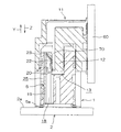
図1(b)および図2を参照して、各側壁14,15の外側面14b,15bには、横並びで(左右方向Xに沿って並んで)多数の縦長の開口25が形成されている。開口25は、各側壁14,15の高さ方向(すなわち連結方向Y)の概ね中央部に配置されている。
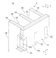
側壁14,15は同様の構成である。図5を参照して、側壁14は、相隣接する端子保持孔18,18間を仕切る仕切り壁26を有しており、上記の開口25は各仕切り壁26に対応して側壁14の外側面14bに形成されている。開口25は、対応する仕切り壁26の一部を切り欠いて形成されており、一対の連通部25a(図5では一方の連通部25aのみを示す)を介して両側の端子保持孔18に通ずる。これにより、各開口25は当該開口25に対応する仕切り壁26を挟んで対向する一対の端子保持孔18,18をそれぞれハウジング3の外部に開放させる。
【0020】
図6は金型によりハウジング3の図5に示す部分を射出成形するときの模式図である。金型30において、上記の開口25を形成するための開口形成用ピン31が、それぞれ、金型30の相隣接する端子保持孔形成用リブ32の間に介在することになる。したがって、射出成形時に端子保持孔形成用リブ32の変形を抑制できるので、狭ピッチで配列される端子保持孔18や仕切り壁26の位置精度を高くすることができ、ひいては端子4,5の位置精度を高くして小型で信頼性の高い電気コネクタ1を提供することができる。
【0021】
特に、開口25が各側壁14,15の高さ方向(すなわち連結方向Y)の概ね中央部に配置されるので、射出成形時の端子保持孔形成用リブ32の変形を確実に防止することができる。
なお、本発明は上記実施の形態に限定されるものではなく、本発明の範囲で種々の変更を施すことができる。
【図面の簡単な説明】
【図1】(a)および(b)は本発明の一実施の形態の電気コネクタの平面図および側面図である。
【図2】図1(b)のII−II線に沿う断面図である。
【図3】図1(b)のIII −III 線に沿う断面図である。
【図4】電気コネクタを対応するプラグ型電気コネクタに接続した状態の概略断面図である。
【図5】電気コネクタの側壁の一部破断拡大斜視図ある。
【図6】金型の構成を示す模式的斜視図である。
【符号の説明】
1 (リセプタクル型)電気コネクタ(基板用電気コネクタ)
2 回路基板
2a 表面
3 ハウジング
3a 対向面
4,5 (信号用)端子
6 (電源用)端子
11 (プラグ型)電気コネクタ
12 連結凸部
13 連結凹部
14,15 側壁
14a,15a 連結側端面
14b,15b 外側面
18 端子保持孔
19 主体部
20 弾性屈曲部
21 突出部
22 接点部
23 当接端部
25 開口
26 仕切り壁
30 金型
31 開口形成用ピン
32 端子保持孔形成用リブ
40 開放部分
X 左右方向
Y 連結方向(高さ方向)
Z (連結方向)の反対方向[0001]
BACKGROUND OF THE INVENTION
The present invention relates to an electrical connector for a board that is attached to the surface of a circuit board.
[0002]
[Prior art]
In recent years, there has been a remarkable spread of personal computers. Among them, a pair of electrical connectors for board-to-board (board-to-board) connection and a pair of electrical connectors for wire-to-board (wire-to-board) connection are provided.
For example, an electrical connector fixed to the surface of a power board that controls the power source and an electrical connector fixed to a motherboard on which the CPU is mounted are connected. One electrical connector is a plug type having a connecting convex portion, and the other electrical connector is a receptacle type having a connecting concave portion.
[0003]
Conventionally, as this type of receptacle-type electrical connector, there has been provided a connector in which terminal holding holes are provided in each of a pair of side walls for partitioning a connection recess, and are opened in the connector connection direction (for example, Patent Document 1).
[0004]
[Patent Document 1]
Japanese Patent Laid-Open No. 11-67364
[Problems to be solved by the invention]
By the way, with the demand for miniaturization and high functionality of the personal computer main body, there is a demand for miniaturization and multipolarization in this type of electrical connector.
Typically, the depth of the terminal holding holes between this type of electrical connectors is 12 to 13 mm, while the width of the terminal holding holes is about 0.4 mm, for example, and the arrangement interval is, for example, 0. There is a request to make it about 6 mm. In this case, the thickness of the partition wall between adjacent terminal holding holes is very thin, for example, 0.1 mm.
[0006]
Therefore, if the connector of
That is, in the mold for molding the housing, the terminal holding hole forming rib for forming the terminal holding hole is also thin (for example, 0.4 mm) and has a narrow pitch (for example, 0.6 mm), The terminal holding hole forming rib may be deformed by the pressure at the time of injection molding. If the rib is deformed during injection molding, the thin partition wall between the terminal holding holes (for example, thickness 0.1 mm) is also deformed and the position accuracy of the terminal holding hole is deteriorated, and consequently the position accuracy of the terminal is deteriorated. The reliability of the electrical connection is reduced.
[0007]
The present invention has been made in view of the above problems, and an object of the present invention is to provide a small-sized and highly reliable electrical connector for a board that can increase the positional accuracy of terminals arranged at a narrow pitch.
[0008]
[Means for Solving the Problems]
In order to achieve the above object, the present invention comprises a housing made of an insulating synthetic resin having a connecting recess that opens in the connecting direction, and a plurality of terminals held side by side by the housing. A pair of opposing side walls extending in the lateral direction to partition the connection recess between the terminal holding holes penetrating each side wall in the connecting direction, a partition wall partitioning adjacent terminal holding holes, and each partition A plurality of openings formed by notching a part of the wall and opening to the outer surface of the side wall, and each opening communicates with a pair of terminal holding holes facing each other across the partition wall in which the opening is formed It is characterized by being opened to the outside while being made .
[0009]
In the present invention, when the housing is injection-molded in the mold, the pins for forming the openings on the outer surface of the partition wall are respectively interposed between the terminal holding hole forming ribs adjacent to the mold. Will do. Accordingly, deformation of the terminal holding hole forming rib can be suppressed during injection molding, so that the positional accuracy of the terminal holding holes (partition walls) arranged at a narrow pitch can be increased, and as a result, the terminal positional accuracy can be increased. A small and highly reliable electrical connector can be provided.
[0010]
It is preferable that the opening on the outer side surface of the side wall is disposed at a substantially central portion in the height direction of the side wall in order to reliably suppress deformation of the terminal holding hole forming rib during injection molding.
[0011]
DETAILED DESCRIPTION OF THE INVENTION
Preferred embodiments of the present invention will be described with reference to the accompanying drawings.
FIGS. 1A and 1B are a plan view and a side view of a board electrical connector according to an embodiment of the present invention. 2 is a cross-sectional view taken along line II-II in FIG. 1B, and FIG. 3 is a cross-sectional view taken along line III-III in FIG.
The
[0012]
Referring to FIG. 2, an
1A and 1B, the
[0013]
Further, in the facing
On the other hand, as shown in FIG. 3, the
[0014]
Further, as shown in FIG. 1B, a pair of
[0015]
Referring to FIGS. 1A and 1B, the
[0016]
Referring to FIG. 1A, the connecting
Referring to FIG. 2, a large number of terminal holding holes 18 are arranged side by side (side by side in the left-right direction X of FIG. 1) on each of the
[0017]
The
Referring to FIG. 2, the terminal 4 is connected to a long
[0018]
The
As shown in FIG. 4, the
[0019]
Referring to FIG. 1B and FIG. 2, a large number of vertically
The
[0020]
FIG. 6 is a schematic view when the portion shown in FIG. 5 of the
[0021]
In particular, since the
The present invention is not limited to the above embodiment, and various modifications can be made within the scope of the present invention.
[Brief description of the drawings]
FIGS. 1A and 1B are a plan view and a side view of an electrical connector according to an embodiment of the present invention.
FIG. 2 is a cross-sectional view taken along line II-II in FIG.
FIG. 3 is a cross-sectional view taken along line III-III in FIG.
FIG. 4 is a schematic cross-sectional view of a state in which the electrical connector is connected to a corresponding plug-type electrical connector.
FIG. 5 is a partially broken enlarged perspective view of a side wall of the electrical connector.
FIG. 6 is a schematic perspective view showing a configuration of a mold.
[Explanation of symbols]
1 (Receptacle type) Electrical connector (Electric connector for PCB)
2
Opposite direction of Z (connection direction)
Claims (2)
上記ハウジングは、互いの間に連結凹部を区画するために横方向に延びる相対向する一対の側壁と、各側壁を上記連結方向に貫通する端子保持孔と、隣接する端子保持孔間を仕切る仕切り壁と、各仕切り壁の一部をそれぞれ切り欠いて形成され側壁の外側面に開放する多数の開口とを含み、
各開口は、当該開口が形成された仕切り壁を挟んで対向する一対の端子保持孔を互いに連通させつつ外部に開放させることを特徴とする基板用電気コネクタ。A housing made of an insulating synthetic resin having a connecting recess that opens in the connecting direction, and a plurality of terminals held side by side by the housing;
The housing includes a pair of opposing side walls extending in the lateral direction so as to divide a connection recess between each other, a terminal holding hole penetrating each side wall in the connection direction, and a partition for partitioning between adjacent terminal holding holes. A plurality of openings that are formed by cutting out a part of each partition wall and open to the outer surface of the side wall;
An electrical connector for a board, wherein each opening is opened to the outside while a pair of terminal holding holes facing each other across a partition wall in which the opening is formed communicate with each other .
Priority Applications (8)
| Application Number | Priority Date | Filing Date | Title |
|---|---|---|---|
| JP2002342765A JP3961937B2 (en) | 2002-11-26 | 2002-11-26 | Board electrical connector |
| AU2003284629A AU2003284629A1 (en) | 2002-11-26 | 2003-11-21 | Electrical connector for board, method of molding electrical connector housing for board, and metal mold for injection molding of electrical connector housing |
| KR1020047011742A KR100622968B1 (en) | 2002-11-26 | 2003-11-21 | Electric connector for boards |
| PCT/JP2003/014899 WO2004049520A1 (en) | 2002-11-26 | 2003-11-21 | Electrical connector for board, method of molding electrical connector housing for board, and metal mold for injection molding of electrical connector housing |
| CNB200380100129XA CN100414787C (en) | 2002-11-26 | 2003-11-21 | Electric connector for boards, method of molding electrical connector housing for board, and metal mold for injection molding of electrical connector housing |
| US10/500,860 US7029333B2 (en) | 2002-11-26 | 2003-11-21 | Electrical connector for boards and method of making |
| EP03774139A EP1475865B1 (en) | 2002-11-26 | 2003-11-21 | Electrical connector for board, method of molding electrical connector housing for board, and metal mold for injection molding of electrical connector housing |
| TW092133170A TWI234908B (en) | 2002-11-26 | 2003-11-26 | Electrical connector for board, method of forming electrical connector housing for board, and metal mold for injection molding of electrical connector housing |
Applications Claiming Priority (1)
| Application Number | Priority Date | Filing Date | Title |
|---|---|---|---|
| JP2002342765A JP3961937B2 (en) | 2002-11-26 | 2002-11-26 | Board electrical connector |
Publications (2)
| Publication Number | Publication Date |
|---|---|
| JP2004178927A JP2004178927A (en) | 2004-06-24 |
| JP3961937B2 true JP3961937B2 (en) | 2007-08-22 |
Family
ID=32375900
Family Applications (1)
| Application Number | Title | Priority Date | Filing Date |
|---|---|---|---|
| JP2002342765A Expired - Fee Related JP3961937B2 (en) | 2002-11-26 | 2002-11-26 | Board electrical connector |
Country Status (8)
| Country | Link |
|---|---|
| US (1) | US7029333B2 (en) |
| EP (1) | EP1475865B1 (en) |
| JP (1) | JP3961937B2 (en) |
| KR (1) | KR100622968B1 (en) |
| CN (1) | CN100414787C (en) |
| AU (1) | AU2003284629A1 (en) |
| TW (1) | TWI234908B (en) |
| WO (1) | WO2004049520A1 (en) |
Families Citing this family (8)
| Publication number | Priority date | Publication date | Assignee | Title |
|---|---|---|---|---|
| ES2527068T3 (en) | 2002-10-23 | 2015-01-19 | University Of Utah Research Foundation | Fusion analysis of amplicons with saturation dyes |
| US9657347B2 (en) | 2004-04-20 | 2017-05-23 | University of Utah Research Foundation and BioFire Defense, LLC | Nucleic acid melting analysis with saturation dyes |
| US7549869B1 (en) * | 2008-06-12 | 2009-06-23 | Cheng Uei Precision Industry Co., Ltd. | Connector |
| TWI391058B (en) * | 2009-08-18 | 2013-03-21 | Pegatron Corp | Mainboard and portable electronic device using the same |
| CN202855994U (en) * | 2012-09-29 | 2013-04-03 | 富士康(昆山)电脑接插件有限公司 | Electric connector |
| JP6064847B2 (en) * | 2013-09-17 | 2017-01-25 | 株式会社デンソー | Fuel pump |
| DE102016013900A1 (en) | 2016-11-22 | 2017-05-24 | Daimler Ag | Method for operating an assistance system |
| US10587062B2 (en) * | 2018-07-24 | 2020-03-10 | Te Connectivity Corporation | Housing post for an electrical assembly |
Family Cites Families (13)
| Publication number | Priority date | Publication date | Assignee | Title |
|---|---|---|---|---|
| US3697933A (en) * | 1971-04-05 | 1972-10-10 | Berg Electronics Inc | Connector block |
| US3966290A (en) * | 1974-06-11 | 1976-06-29 | Amp Incorporated | Polarized connector |
| US5842874A (en) * | 1994-05-25 | 1998-12-01 | Molex Incorporated | Dual housing board-to-board connector |
| JP2932152B2 (en) * | 1994-07-19 | 1999-08-09 | モレックス インコーポレーテッド | Terminal for electrical connector and method of forming electrical connector |
| US6159021A (en) * | 1995-02-09 | 2000-12-12 | The Whitaker Corporation | Electrical connector for printed circuit boards |
| JP3023276U (en) * | 1995-09-07 | 1996-04-16 | モレックス インコーポレーテッド | Electrical connector |
| JP3350843B2 (en) * | 1996-12-20 | 2002-11-25 | モレックス インコーポレーテッド | Method of manufacturing electrical connector with insert mold |
| JPH10284197A (en) * | 1997-04-07 | 1998-10-23 | Kueizaa Syst:Kk | Electrical connector and manufacture thereof |
| JP3871160B2 (en) | 1997-08-08 | 2007-01-24 | タイコエレクトロニクスアンプ株式会社 | Board mounted connector |
| JP3266556B2 (en) | 1997-09-30 | 2002-03-18 | 日本航空電子工業株式会社 | Connector mold and method of manufacturing connector |
| JP2001001372A (en) * | 1999-06-23 | 2001-01-09 | Fujitsu Takamisawa Component Ltd | Injection mold and production of connector insulator |
| TW445676B (en) * | 1999-06-24 | 2001-07-11 | Hon Hai Prec Ind Co Ltd | Electrical connector structure |
| CN2431654Y (en) * | 2000-05-31 | 2001-05-23 | 莫列斯公司 | Improved structure for connector terminal |
-
2002
- 2002-11-26 JP JP2002342765A patent/JP3961937B2/en not_active Expired - Fee Related
-
2003
- 2003-11-21 EP EP03774139A patent/EP1475865B1/en not_active Expired - Fee Related
- 2003-11-21 WO PCT/JP2003/014899 patent/WO2004049520A1/en active Application Filing
- 2003-11-21 CN CNB200380100129XA patent/CN100414787C/en not_active Expired - Fee Related
- 2003-11-21 AU AU2003284629A patent/AU2003284629A1/en not_active Abandoned
- 2003-11-21 KR KR1020047011742A patent/KR100622968B1/en not_active IP Right Cessation
- 2003-11-21 US US10/500,860 patent/US7029333B2/en not_active Expired - Fee Related
- 2003-11-26 TW TW092133170A patent/TWI234908B/en not_active IP Right Cessation
Also Published As
| Publication number | Publication date |
|---|---|
| JP2004178927A (en) | 2004-06-24 |
| CN100414787C (en) | 2008-08-27 |
| AU2003284629A1 (en) | 2004-06-18 |
| KR100622968B1 (en) | 2006-09-14 |
| CN1685575A (en) | 2005-10-19 |
| US7029333B2 (en) | 2006-04-18 |
| US20050079742A1 (en) | 2005-04-14 |
| KR20040078681A (en) | 2004-09-10 |
| WO2004049520A1 (en) | 2004-06-10 |
| TW200414633A (en) | 2004-08-01 |
| EP1475865A1 (en) | 2004-11-10 |
| EP1475865B1 (en) | 2012-01-11 |
| TWI234908B (en) | 2005-06-21 |
| EP1475865A4 (en) | 2006-08-02 |
Similar Documents
| Publication | Publication Date | Title |
|---|---|---|
| US7637786B2 (en) | Electrical connector | |
| US7351106B2 (en) | Electrical connector having an inner printed circuit board | |
| JP4592462B2 (en) | Board connector | |
| US20050112952A1 (en) | Power jack connector | |
| JP7445703B2 (en) | connector | |
| EP1878093A1 (en) | Board-to-board connector pair | |
| JP2002367697A (en) | Contact and electric connector installed with the same | |
| JP7454995B2 (en) | Connectors and connector pairs | |
| US8187031B2 (en) | Electrical connector with an improved board lock | |
| US20030166347A1 (en) | Low-profile connector for circuit boards | |
| JP3916775B2 (en) | connector | |
| US6447307B1 (en) | Electrical connector having spacer | |
| JP3961937B2 (en) | Board electrical connector | |
| US6575783B1 (en) | Electrical connector assembly with retaining frame | |
| EP1467439B1 (en) | Electrical connector | |
| US7077674B2 (en) | Board attachment type electrical connector | |
| JP4883670B2 (en) | Electrical connector | |
| KR100552322B1 (en) | Electrical connector | |
| JP2002141124A (en) | Substrate fixing type connector and substrate fixing structure for connector | |
| JP2004527069A (en) | Small board-to-board connector | |
| JPH0487172A (en) | Electric connector | |
| US6302710B1 (en) | Electrical connector assembly for vertically connecting two electrical devices together | |
| JP7283971B2 (en) | BOARD CONNECTOR AND BOARD CONNECTOR STRUCTURE | |
| US6902442B2 (en) | Electrical connector | |
| US7048558B2 (en) | Memory card connector |
Legal Events
| Date | Code | Title | Description |
|---|---|---|---|
| A621 | Written request for application examination |
Free format text: JAPANESE INTERMEDIATE CODE: A621 Effective date: 20050810 |
|
| A131 | Notification of reasons for refusal |
Free format text: JAPANESE INTERMEDIATE CODE: A131 Effective date: 20070206 |
|
| A521 | Request for written amendment filed |
Free format text: JAPANESE INTERMEDIATE CODE: A523 Effective date: 20070405 |
|
| TRDD | Decision of grant or rejection written | ||
| A01 | Written decision to grant a patent or to grant a registration (utility model) |
Free format text: JAPANESE INTERMEDIATE CODE: A01 Effective date: 20070515 |
|
| A61 | First payment of annual fees (during grant procedure) |
Free format text: JAPANESE INTERMEDIATE CODE: A61 Effective date: 20070517 |
|
| R150 | Certificate of patent or registration of utility model |
Ref document number: 3961937 Country of ref document: JP Free format text: JAPANESE INTERMEDIATE CODE: R150 Free format text: JAPANESE INTERMEDIATE CODE: R150 |
|
| FPAY | Renewal fee payment (event date is renewal date of database) |
Free format text: PAYMENT UNTIL: 20110525 Year of fee payment: 4 |
|
| R250 | Receipt of annual fees |
Free format text: JAPANESE INTERMEDIATE CODE: R250 |
|
| FPAY | Renewal fee payment (event date is renewal date of database) |
Free format text: PAYMENT UNTIL: 20120525 Year of fee payment: 5 |
|
| R250 | Receipt of annual fees |
Free format text: JAPANESE INTERMEDIATE CODE: R250 |
|
| FPAY | Renewal fee payment (event date is renewal date of database) |
Free format text: PAYMENT UNTIL: 20130525 Year of fee payment: 6 |
|
| R250 | Receipt of annual fees |
Free format text: JAPANESE INTERMEDIATE CODE: R250 |
|
| FPAY | Renewal fee payment (event date is renewal date of database) |
Free format text: PAYMENT UNTIL: 20140525 Year of fee payment: 7 |
|
| R250 | Receipt of annual fees |
Free format text: JAPANESE INTERMEDIATE CODE: R250 |
|
| R250 | Receipt of annual fees |
Free format text: JAPANESE INTERMEDIATE CODE: R250 |
|
| R250 | Receipt of annual fees |
Free format text: JAPANESE INTERMEDIATE CODE: R250 |
|
| R250 | Receipt of annual fees |
Free format text: JAPANESE INTERMEDIATE CODE: R250 |
|
| R250 | Receipt of annual fees |
Free format text: JAPANESE INTERMEDIATE CODE: R250 |
|
| R250 | Receipt of annual fees |
Free format text: JAPANESE INTERMEDIATE CODE: R250 |
|
| R250 | Receipt of annual fees |
Free format text: JAPANESE INTERMEDIATE CODE: R250 |
|
| R250 | Receipt of annual fees |
Free format text: JAPANESE INTERMEDIATE CODE: R250 |
|
| R250 | Receipt of annual fees |
Free format text: JAPANESE INTERMEDIATE CODE: R250 |
|
| LAPS | Cancellation because of no payment of annual fees |