JP3956748B2 - Display device, driving circuit thereof, driving method thereof, and electronic apparatus - Google Patents
Display device, driving circuit thereof, driving method thereof, and electronic apparatus Download PDFInfo
- Publication number
- JP3956748B2 JP3956748B2 JP2002108533A JP2002108533A JP3956748B2 JP 3956748 B2 JP3956748 B2 JP 3956748B2 JP 2002108533 A JP2002108533 A JP 2002108533A JP 2002108533 A JP2002108533 A JP 2002108533A JP 3956748 B2 JP3956748 B2 JP 3956748B2
- Authority
- JP
- Japan
- Prior art keywords
- voltage
- scanning line
- scanning
- block
- selection voltage
- Prior art date
- Legal status (The legal status is an assumption and is not a legal conclusion. Google has not performed a legal analysis and makes no representation as to the accuracy of the status listed.)
- Expired - Fee Related
Links
Images


Classifications
-
- G—PHYSICS
- G09—EDUCATION; CRYPTOGRAPHY; DISPLAY; ADVERTISING; SEALS
- G09G—ARRANGEMENTS OR CIRCUITS FOR CONTROL OF INDICATING DEVICES USING STATIC MEANS TO PRESENT VARIABLE INFORMATION
- G09G3/00—Control arrangements or circuits, of interest only in connection with visual indicators other than cathode-ray tubes
- G09G3/20—Control arrangements or circuits, of interest only in connection with visual indicators other than cathode-ray tubes for presentation of an assembly of a number of characters, e.g. a page, by composing the assembly by combination of individual elements arranged in a matrix no fixed position being assigned to or needed to be assigned to the individual characters or partial characters
- G09G3/34—Control arrangements or circuits, of interest only in connection with visual indicators other than cathode-ray tubes for presentation of an assembly of a number of characters, e.g. a page, by composing the assembly by combination of individual elements arranged in a matrix no fixed position being assigned to or needed to be assigned to the individual characters or partial characters by control of light from an independent source
- G09G3/36—Control arrangements or circuits, of interest only in connection with visual indicators other than cathode-ray tubes for presentation of an assembly of a number of characters, e.g. a page, by composing the assembly by combination of individual elements arranged in a matrix no fixed position being assigned to or needed to be assigned to the individual characters or partial characters by control of light from an independent source using liquid crystals
- G09G3/3611—Control of matrices with row and column drivers
- G09G3/367—Control of matrices with row and column drivers with a nonlinear element in series with the liquid crystal cell, e.g. a diode, or M.I.M. element
-
- G—PHYSICS
- G09—EDUCATION; CRYPTOGRAPHY; DISPLAY; ADVERTISING; SEALS
- G09G—ARRANGEMENTS OR CIRCUITS FOR CONTROL OF INDICATING DEVICES USING STATIC MEANS TO PRESENT VARIABLE INFORMATION
- G09G3/00—Control arrangements or circuits, of interest only in connection with visual indicators other than cathode-ray tubes
- G09G3/20—Control arrangements or circuits, of interest only in connection with visual indicators other than cathode-ray tubes for presentation of an assembly of a number of characters, e.g. a page, by composing the assembly by combination of individual elements arranged in a matrix no fixed position being assigned to or needed to be assigned to the individual characters or partial characters
- G09G3/34—Control arrangements or circuits, of interest only in connection with visual indicators other than cathode-ray tubes for presentation of an assembly of a number of characters, e.g. a page, by composing the assembly by combination of individual elements arranged in a matrix no fixed position being assigned to or needed to be assigned to the individual characters or partial characters by control of light from an independent source
- G09G3/36—Control arrangements or circuits, of interest only in connection with visual indicators other than cathode-ray tubes for presentation of an assembly of a number of characters, e.g. a page, by composing the assembly by combination of individual elements arranged in a matrix no fixed position being assigned to or needed to be assigned to the individual characters or partial characters by control of light from an independent source using liquid crystals
- G09G3/3611—Control of matrices with row and column drivers
- G09G3/3674—Details of drivers for scan electrodes
-
- G—PHYSICS
- G09—EDUCATION; CRYPTOGRAPHY; DISPLAY; ADVERTISING; SEALS
- G09G—ARRANGEMENTS OR CIRCUITS FOR CONTROL OF INDICATING DEVICES USING STATIC MEANS TO PRESENT VARIABLE INFORMATION
- G09G3/00—Control arrangements or circuits, of interest only in connection with visual indicators other than cathode-ray tubes
- G09G3/20—Control arrangements or circuits, of interest only in connection with visual indicators other than cathode-ray tubes for presentation of an assembly of a number of characters, e.g. a page, by composing the assembly by combination of individual elements arranged in a matrix no fixed position being assigned to or needed to be assigned to the individual characters or partial characters
- G09G3/34—Control arrangements or circuits, of interest only in connection with visual indicators other than cathode-ray tubes for presentation of an assembly of a number of characters, e.g. a page, by composing the assembly by combination of individual elements arranged in a matrix no fixed position being assigned to or needed to be assigned to the individual characters or partial characters by control of light from an independent source
- G09G3/36—Control arrangements or circuits, of interest only in connection with visual indicators other than cathode-ray tubes for presentation of an assembly of a number of characters, e.g. a page, by composing the assembly by combination of individual elements arranged in a matrix no fixed position being assigned to or needed to be assigned to the individual characters or partial characters by control of light from an independent source using liquid crystals
- G09G3/3611—Control of matrices with row and column drivers
- G09G3/3685—Details of drivers for data electrodes
-
- G—PHYSICS
- G09—EDUCATION; CRYPTOGRAPHY; DISPLAY; ADVERTISING; SEALS
- G09G—ARRANGEMENTS OR CIRCUITS FOR CONTROL OF INDICATING DEVICES USING STATIC MEANS TO PRESENT VARIABLE INFORMATION
- G09G2320/00—Control of display operating conditions
- G09G2320/02—Improving the quality of display appearance
- G09G2320/0209—Crosstalk reduction, i.e. to reduce direct or indirect influences of signals directed to a certain pixel of the displayed image on other pixels of said image, inclusive of influences affecting pixels in different frames or fields or sub-images which constitute a same image, e.g. left and right images of a stereoscopic display
-
- G—PHYSICS
- G09—EDUCATION; CRYPTOGRAPHY; DISPLAY; ADVERTISING; SEALS
- G09G—ARRANGEMENTS OR CIRCUITS FOR CONTROL OF INDICATING DEVICES USING STATIC MEANS TO PRESENT VARIABLE INFORMATION
- G09G3/00—Control arrangements or circuits, of interest only in connection with visual indicators other than cathode-ray tubes
- G09G3/20—Control arrangements or circuits, of interest only in connection with visual indicators other than cathode-ray tubes for presentation of an assembly of a number of characters, e.g. a page, by composing the assembly by combination of individual elements arranged in a matrix no fixed position being assigned to or needed to be assigned to the individual characters or partial characters
- G09G3/2007—Display of intermediate tones
- G09G3/2014—Display of intermediate tones by modulation of the duration of a single pulse during which the logic level remains constant
-
- G—PHYSICS
- G09—EDUCATION; CRYPTOGRAPHY; DISPLAY; ADVERTISING; SEALS
- G09G—ARRANGEMENTS OR CIRCUITS FOR CONTROL OF INDICATING DEVICES USING STATIC MEANS TO PRESENT VARIABLE INFORMATION
- G09G3/00—Control arrangements or circuits, of interest only in connection with visual indicators other than cathode-ray tubes
- G09G3/20—Control arrangements or circuits, of interest only in connection with visual indicators other than cathode-ray tubes for presentation of an assembly of a number of characters, e.g. a page, by composing the assembly by combination of individual elements arranged in a matrix no fixed position being assigned to or needed to be assigned to the individual characters or partial characters
- G09G3/34—Control arrangements or circuits, of interest only in connection with visual indicators other than cathode-ray tubes for presentation of an assembly of a number of characters, e.g. a page, by composing the assembly by combination of individual elements arranged in a matrix no fixed position being assigned to or needed to be assigned to the individual characters or partial characters by control of light from an independent source
- G09G3/36—Control arrangements or circuits, of interest only in connection with visual indicators other than cathode-ray tubes for presentation of an assembly of a number of characters, e.g. a page, by composing the assembly by combination of individual elements arranged in a matrix no fixed position being assigned to or needed to be assigned to the individual characters or partial characters by control of light from an independent source using liquid crystals
- G09G3/3611—Control of matrices with row and column drivers
- G09G3/3614—Control of polarity reversal in general
Landscapes
- Engineering & Computer Science (AREA)
- Chemical & Material Sciences (AREA)
- Crystallography & Structural Chemistry (AREA)
- Physics & Mathematics (AREA)
- Computer Hardware Design (AREA)
- General Physics & Mathematics (AREA)
- Theoretical Computer Science (AREA)
- Liquid Crystal (AREA)
- Control Of Indicators Other Than Cathode Ray Tubes (AREA)
- Liquid Crystal Display Device Control (AREA)
Description
【0001】
【発明の属する技術分野】
本発明は、例えば、薄膜ダイオードによって画素をスイッチングする構成において、表示品位の低下を抑えつつ低消費電力化を図った表示装置、その駆動回路、その駆動方法、および、電子機器に関する。
【0002】
【従来の技術】
近年、液晶の電気光学的変化を用いた表示装置が、薄型・小型・低消費電力等いった特長を生かして、陰極線管(CRT)に代わるディスプレイ・デバイスとして、各種電子機器やテレビジョンなどに広く用いられつつある。
【0003】
この表示装置は、駆動方式等によって分類すると、スイッチングにより画素を駆動するアクティブ・マトリクス型と、スイッチング素子を用いないで画素を駆動するパッシブ・マトリクス型とに大別することができる。このうち、前者に係るアクティブ・マトリクス型では、スイッチング素子の種類によって、さらに、薄膜トランジスタ(TFT:Thin Film Transistor)などの三端子型スイッチング素子を用いる型と、薄膜ダイオード(TFD:Thin Film Diode)などの二端子型スイッチング素子を用いる型とに大別することができるが、後者の二端子型スイッチング素子を用いる型の方が、配線の交差部分がないために、配線間の短絡不良が原理的に発生しない点、成膜工程およびフォトリソグラフィ工程を短縮できる点、さらに低消費電力に向いている点において有利とされている。
【0004】
一方、二端子型スイッチング素子によって画素をスイッチングする表示装置においては、表示品位を低下させる様々なモードが存在する。ただし、最終的には、データ線(セグメント電極)がとり得る2つの電圧が印加される期間の割合が、いかなるパターンを表示させたとしても半分ずつとなる、という4値駆動法(1/2Hセレクト、1H反転)を採用すると、このような表示品位の低下を解消することが知られている。
【0005】
ところで、特にPDA(Personal Digital Assistant)や携帯電話などのような携帯型電子機器にあっては、電池駆動が原則であるため、低消費電力であることの要求が強い。このため、携帯型電子機器に適用される表示装置にも、低消費電力であることが強く求められている。
【0006】
さらに、この種の携帯型電子機器には、近年、音楽再生のような様々な機能が追加されつつあり、こうした新機能に割り当てられる電力を捻出するためにも、表示装置の消費電力についてはたとえ1mWでも削減したい、という要求すら存在している状況にある。
【0007】
一方、近年では、表示装置には、単純な黒白表示のみならず、豊かな中間階調で表示を行う高階調表示化も要求されている。
【0008】
【発明が解決しようとする課題】
しかしながら、上記4値駆動法において、中間階調表示を行うと、データ線の電圧切替頻度が高くなるので、データ線に付随する容量によって無駄に電力が消費される、という欠点があった。一方、上記4値駆動法(1/2Hセレクト、1H反転)を採用しないと、今度は、モードによっては、表示品位が低下する、という問題が発生することになる。
【0009】
本発明は、上述した事情に鑑みてなされたものであり、その目的とするところは、表示示品位の低下を抑えつつ、低消費電力化を図ることが可能な表示装置、その駆動回路、その駆動方法および電子機器を提供することにある。
【0010】
【課題を解決するための手段】
上記目的を達成するために、本発明の実施形態に係る表示装置の駆動回路は、走査線とデータ線との交差に対応して設けられた画素を駆動する表示装置の駆動回路であって、前記走査線を1本ずつ選択して、当該選択した走査線に対して選択電圧を印加する一方、それ以外の走査線に対して非選択電圧を走査線に印加する走査線駆動回路であって、前記走査線を複数本まとめてブロック化し、当該ブロック化されたブロックにおいて、前記選択電圧の極性を、前記データ線に印加されるオン電圧およびオフ電圧の中間値を基準として走査線の1本選択する毎に反転するとともに、前記ブロックにあって最後に選択される走査線の選択電圧と当該ブロックの次のブロックにあって最初に選択される走査線の選択電圧との極性を同一とする走査線駆動回路と、データ線に対し、前記走査線が選択されて選択電圧が印加されたときに、当該走査線と当該データ線との交差に対応する画素にて表示すべき内容と当該選択電圧の極性とに応じてオン電圧またはオフ電圧を印加するデータ線駆動回路とを具備する構成を特徴としている。
【0011】
この構成によれば、一のデータ線において点灯画素と非点灯画素とが交互に現れる場合であっても、当該データ線に印加される電圧実効値と、他のデータ線に印加される電圧実効値との差が少なくなるので、表示品位の低下が抑えられる。さらに、一のデータ線において中間階調の画素が連続する場合であっても、当該データ線に印加されるデータ電圧の切替頻度が少なくなるので、データ線やその駆動回路に付随する容量の充放電によって無駄に消費される電力が抑えられて、その分、低消費電力化を図ることが可能となる。
【0012】
なお、本件における点灯電圧とは、ある1本の走査線が選択された期間に着目した場合に、その期間において印加される選択電圧とは逆極性にあるデータ信号電圧をいい、また、非点灯電圧とは、同じくある1本の走査線が選択された期間において印加される選択電圧とは同一極性にあるデータ信号電圧をいう。
【0013】
この構成によれば、一のデータ線において点灯画素と非点灯画素とが交互に現れる場合であっても、当該データ線の電圧実効値に偏りは生じないが、表示パターンによっては、偏りが発生するときがある。例えば、ブロックにおける選択電圧の極性に対応して点灯画素と非点灯画素とが配列するような表示をさせると、データ線の電圧実効値に偏りが発生する。
【0014】
そこで、上記構成において、前記ブロックを構成する走査線数と当該ブロックの次のブロックを構成する走査線数とが異なる構成が好ましい。このような構成にすると、偏りを発生させるパターンの出現率が低くなるので、表示品位の低下をより抑えることができる。
【0015】
また、上記駆動回路において、ブロックの境界に相当する走査線では、選択電圧の極性が、他の部分とは異なり同一であるので、表示に差が発生しやすい。そこで、上記構成において、前記データ線駆動回路は、前記ブロックにあって最初に選択された走査線に選択電圧が印加されたとき、または、前記ブロックにあって最後に選択された走査線に選択電圧が印加されたときの少なくとも一方において、前記オン電圧または前記オフ電圧を補正によって、表示の差を少なくすることができる。
【0016】
このような表示の差を少なくするためには、データ線駆動回路の側における補正のほか、走査線駆動回路の側における補正でも可能である。すなわち、前記走査線駆動回路は、一のブロックにあって最初に選択された走査線に選択電圧が印加されたとき、または、一のブロックにあって最後に選択された走査線に選択電圧が印加されたときの少なくとも一方において、当該選択電圧または当該選択電圧印加時間を補正する構成が好ましい。この構成によれば、選択電圧それ自体、または、選択時間を印加する時間の補正によって、表示の差を少なくすることができる。
【0017】
一方、走査線駆動回路は、前記ブロックの境界が垂直走査期間毎に順次シフトするように、前記走査線のブロック化を実行する構成も好ましい。この構成によれば、ブロックの境界部分が、時間経過とともに移動するので、当該部分において表示差が発生していても目立たなくなる結果、表示品位の低下として視認されにくい。
【0018】
このようにブロックの境界を順次シフトさせる構成において、走査線駆動回路は、一のブロックにあって最初または最後に選択される走査線に対し、前記選択電圧に替えて前記非選択電圧を印加しても良い。こうすると、ブロックの境界部分における書込がスキップされるので、表示差の発生を抑えることができる。
【0019】
また、前記データ線駆動回路は、前記ブロックにあって最初または最後に選択される走査線に選択電圧が印加されたとき、前記オン電圧または前記オフ電圧を補正しても、同様に、表示差の発生を抑えることができる。
【0020】
あるいはまた、走査線駆動回路が、一のブロックにあって最初に選択された走査線に選択電圧が印加されたとき、または、一のブロックにあって最後に選択された走査線に選択電圧が印加されたときの少なくとも一方において、当該選択電圧または当該選択電圧印加時間を補正しても、同様に、表示差の発生を抑えることができる。
【0021】
ここで、本発明は、表示装置の駆動方法としても実現できる。すなわち、この駆動方法は、走査線とデータ線との交差に対応して設けられた画素を駆動する表示装置の駆動方法であって、前記走査線を1本ずつ選択して、当該選択した走査線に対して選択電圧を印加する一方、それ以外の走査線に対して非選択電圧を走査線に印加し、かつ、前記走査線を複数本まとめてブロック化し、当該ブロック化されたブロックにあっては、前記選択電圧の極性を、前記データ線に印加されるオン電圧およびオフ電圧の中間値を基準として走査線の1本選択する毎に反転するとともに、前記ブロックにあって最後に選択される走査線の選択電圧と当該ブロックの次のブロックにあって最初に選択される走査線の選択電圧との極性を同一とし、データ線に対し、前記走査線が選択されて選択電圧が印加されたときに、当該走査線と当該データ線との交差に対応する画素にて表示すべき内容と当該選択電圧の極性とに応じてオン電圧またはオフ電圧を印加する方法を特徴としている。
【0022】
この方法によれば、一のデータ線に印加される電圧実効値と、他のデータ線に印加される電圧実効値との差が少なく、また、当該データ線に印加されるデータ電圧の切替頻度も低い。このため、表示品位の低下を抑えた上で、低消費電力化を図ることが可能となる。
【0023】
また、上記目的を達成するため、本発明に係る表示装置は、走査線とデータ線との交差に対応して設けられた画素を備える表示装置であって、前記走査線を1本ずつ選択して、当該選択した走査線に対して選択電圧を印加する一方、それ以外の走査線に対して非選択電圧を走査線に印加する走査線駆動回路であって、前記走査線を複数本まとめてブロック化し、当該ブロック化されたブロックにあっては、前記選択電圧の極性を、前記データ線に印加されるオン電圧およびオフ電圧の中間値を基準として走査線の1本選択する毎に反転するとともに、前記ブロックにあって最後に選択される走査線の選択電圧と当該ブロックの次のブロックにあって最初に選択される走査線の選択電圧との極性を同一とする走査線駆動回路と、データ線に対し、前記走査線が選択されて選択電圧が印加されたときに、当該走査線と当該データ線との交差に対応する画素にて表示すべき内容と当該選択電圧の極性とに応じてオン電圧またはオフ電圧を印加するデータ線駆動回路とを具備する構成を特徴としている。
【0024】
この表示装置によれば、上記駆動回路と同様に、一のデータ線に印加される電圧実効値と、他のデータ線に印加される電圧実効値との差が少なく、また、当該データ線に印加されるデータ電圧の切替頻度も低い。このため、表示品位の低下を抑えた上で、低消費電力化を図ることが可能となる。
【0025】
ここで、本発明に係る表示装置は、複数の走査線と、複数のデータ線と、走査線とデータ線との各交差点に対応して設けられた複数の画素とを有し、それぞれの画素は、画素電極と、画素電極とデータ線との間に設けられた二端子型スイッチング素子とを含み、データ線の延在方向において隣接した画素電極の間に、これらの画素電極と電気的に分離された導電部を介在させることが好ましい。
【0026】
この表示装置によれば、隣接した画素電極の間に介在する導電部が、これらの画素電極間の寄生容量を低減する静電シールドとして機能するため、ブロック境界部における表示むらの発生を抑制する。なお、この導電部は、データ線の一部をデータ線の延在方向とは異なる方向に突出させた突出部であってもよい。また、データ線とは電気的に分離された状態で、データ線の延在方向とは異なる方向に延在し、かつ、それぞれが共通接続された複数の導電線を設けた場合、導電線のそれぞれが導電部に相当する。
【0027】
また、本発明に係る表示装置において、前記画素は、前記走査線または前記データ線のいずれか一方に一端が接続された二端子型スイッチング素子と、前記走査線または前記データ線のいずれか他方と、前記二端子型スイッチング素子の他端に接続された画素電極との間に電気光学物質が挟持された電気光学容量とを含む構成が好ましい。このように二端子型スイッチング素子を用いると、三端子型スイッチング素子を用いた構成と比較して、配線間の短絡不良が原理的に発生しない点や、製造プロセスが簡略化される点などにおいて有利である。
【0028】
さらに、このような二端子型スイッチング素子は、導電体/絶縁体/導電体の構造を有する構成が望ましい。この構成では、いずれかの導電体が、そのまま走査線またはデータ線として用いることが可能であり、また、絶縁体は、該導電体自体を酸化することで形成可能である。
【0029】
また、本発明における電子機器は、上記表示装置を備えるので、表示品位の低下を抑えた上で、低消費電力化等が可能になる。なお、このような電子機器としては、パーソナルコンピュータや、携帯電話、ディジタルスチルカメラなどなどが挙げられる。
【0030】
【発明の実施の形態】
以下、本発明の実施の形態について図面を参照して説明する。
【0031】
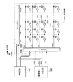
<構成>
はじめに、本発明の実施形態に係る表示装置の電気的な構成について説明する。図1は、この構成を示すブロック図である。
【0032】
この図に示されるように、表示装置100には、複数のデータ線(セグメント電極)212が列(Y)方向に延在して形成される一方、複数の走査線(コモン電極)312が行(X)方向に延在して形成されるとともに、データ線212と走査線312との各交差に対応して画素116が形成されている。さらに、各画素116は、液晶容量118と、二端子型スイッチング素子の一例であるTFD(Thin Film Diode:薄膜ダイオード)220との直列接続からなる。このうち、液晶容量118は、後述するように、画素電極と、対向電極として機能する走査線312との間に、電気光学物質の一例たる液晶を挟持した構成となっている。
【0033】
なお、この実施形態にあっては、説明の便宜上、走査線312の総数を160本とし、データ線212の総数を120本として、160行×120列のマトリクス型表示装置として説明するが、本発明をこれに限定する趣旨ではない。
【0034】
次に、Yドライバ350は、一般には走査線駆動回路と呼ばれるものであり、走査信号Y1、Y2、Y3、…、Y160を、それぞれ1行目、2行目、3行目、…、160行目の走査線312に供給するものである。詳細には、Yドライバ350は、160本の走査線312を後述するような順番で1本ずつ選択して、選択した走査線312には選択電圧を、他の走査線312には非選択電圧を、それぞれ供給するものである。
【0035】
また、Xドライバ250は、一般にはデータ線駆動回路と呼ばれるものであり、Yドライバ350により選択された走査線312に位置する画素116に対し、データ信号X1、X2、X3、…、X120を、表示内容に応じてそれぞれ対応するデータ線212を介して供給するものである。なお、Xドライバ250およびYドライバ350の詳細構成については後述することとする。
【0036】
一方、制御回路400は、Xドライバ250およびYドライバ350に対して、後述する階調データや、各種制御信号、クロック信号などを供給して、両者を制御するものである。また、駆動電圧形成回路500は、電圧±VSと電圧±VD/2とをそれぞれ生成するものである。
【0037】
ここで、本実施形態において、電圧±VSは、走査信号における選択電圧として用いられ、また、電圧±VD/2は、走査信号における非選択電圧と、データ信号におけるデータ電圧とで兼用される構成となっている。なお、非選択電圧とデータ電圧とを兼用するのではなく、異ならせても良いが、駆動電圧形成回路500が生成すべき電圧数が増加する分だけ、構成が複雑化する。
【0038】
また、本実施形態において、走査線312やデータ線212に印加される電圧の極性基準は、データ線212に印加されるデータ電圧±VD/2の中間電圧(仮想電圧)であり、これよりも高電位側を正極とし、低電位側を負極としている。
【0039】
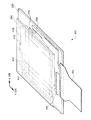
<機械的構成>
次に、本実施形態に係る表示装置の機械的な構成について説明する。図2は、表示装置100の全体構成を示す斜視図であり、図3は、この表示装置100をX方向に沿って破断した場合の構成を示す部分断面図である。
【0040】
これらの図に示されるように、表示装置100は、観察者側に位置する対向基板300と、その背面側に位置する素子基板200とが、スペーサを兼ねる導電性粒子(導通材)114の混入されたシール材110によって一定の間隙を保って貼り合わせられるとともに、この間隙に例えばTN(Twisted Nematic)型の液晶160が封入された構成となっている。なお、シール材110は、図2に示されるように、対向基板300の内周縁に沿って枠状に形成されるが、液晶160を封入するために、その一部が開口している。このため、液晶の封入後に、その開口部分が封止材112によって封止された構成となっている。
【0041】
さて、対向基板300の対向面には、行(X)方向に延在して形成される走査線312のほか、配向膜308が形成されて、所定の方向にラビング処理が施されている。ここで、対向基板300に形成された走査線312は、図3に示されるように、シール材110に分散された導電性粒子114を介し、各走査線312と1対1に対応する配線342であって、素子基板200に形成された配線342の一端に接続されている。すなわち、対向基板300に形成された走査線312は、導電性粒子114および配線342を介して、素子基板200側に引き出された構成となっている。
【0042】
一方、対向基板300の外側(観察側)には偏光子131が貼り付けられて(図2では省略)、その吸収軸が、配向膜308へのラビング処理の方向に対応して設定されている。
【0043】
また、素子基板300の対向面には、Y(列)方向に延在して形成されるデータ線212に隣接して矩形状の画素電極234が形成されるほか、配向膜208が形成されて、所定の方向にラビング処理が施されている。一方、素子基板200の外側(観察側の反対側)には偏光子121が貼り付けられて(図2では省略)、その吸収軸が、配向膜208へのラビング処理の方向に対応して設定されている。このほかに、素子基板200の外側には、均一に光を照射するバックライトユニットが設けられるが、本件とは直接に関係しないので、図示を省略している。
【0044】
続いて表示領域外について説明すると、図2に示されるように、素子基板200にあって対向基板300から張り出した2辺には、データ線212を駆動するためのXドライバ250、および、走査線312を駆動するためのYドライバ350が、それぞれCOG(Chip On Glass)技術により実装されている。これにより、Xドライバ250は、データ線212にデータ信号を直接的に供給する一方、Yドライバ350は、配線342および導電性粒子114を介し、走査線312に走査信号を間接的に供給する構成となっている。
【0045】
また、Xドライバ250が実装される領域の外側近傍には、FPC(Flexible Printed Circuit)基板150が接合されて、制御回路400など(図1参照)による各種信号や電圧信号などが、Yドライバ350およびXドライバ250にそれぞれ供給される構成となっている。
【0046】
なお、図1におけるXドライバ250およびYドライバ350は、図2とは異なり、それぞれ表示装置100の左側および上側にそれぞれ位置しているが、これは、電気的な構成を説明するための便宜上の措置に過ぎない。また、Xドライバ250およびYドライバ350を、それぞれ素子基板200にCOG実装する替わりに、例えば、TAB(Tape Automated Bonding)技術を用いて、各ドライバが実装されたTCP(Tape Carrier Package)を、異方性導電膜により電気的に接続する構成としても良い。
【0047】
<画素の構成>
次に表示装置における画素116の詳細構成について説明する。図4は、その構造を示す部分破断斜視図である。なお、この図では、説明理解のために、図3における配向膜208、308および偏光子121、131が省略されている。
【0048】
さて、図4に示されるように、素子基板200の対向面には、ITO(Indium Tin Oxide)などの透明導電体からなる矩形状の画素電極234がマトリクス状に配列しており、このうち、同一列にて配列する画素電極234が、1本のデータ線212に、それぞれTFD220を介して共通接続されている。ここで、TFD220は、基板側からみると、タンタル単体やタンタル合金などから形成され、かつ、データ線212からT字状に枝分かれした第1の導電体222と、この第1の導電体222を陽極酸化させた絶縁体224と、クロム等などの第2の導電体226とから構成されて、導電体/絶縁体/導電体のサンドイッチ構造を採る。このため、TFD220は、電流−電圧特性が正負双方向にわたって非線形となるダイオードスイッチング特性を有することになる。
【0049】
なお、素子基板200の上面には、下地として透明性を有する絶縁膜201が形成されている。詳細には、この絶縁膜201は、第2の導電体226の堆積後における熱処理により、第1の導電体222が剥離しないようにするため、および、第1の導電体222に不純物が拡散しないようにするために、設けられている。したがって、これらが問題とならない場合には、絶縁膜201は省略可能である。
【0050】
一方、対向基板300の対向面には、ITOなどからなる走査線312が、データ線212とは直交する行方向に延在し、かつ、画素電極234の対向する位置に配列している。これにより、走査線312は、画素電極234の対向電極として機能することになる。したがって、図1における液晶容量118は、データ線212と走査線312との交差において、当該走査線312と、画素電極234と、両者の間に挟持された液晶160とによって構成されることになる。
【0051】
このような構成において、データ線212に印加されているデータ電圧にかかわらず、TFD220がオンする選択電圧を走査線312に印加すると、当該走査線312および当該データ線212の交差に対応するTFD220がオンして、オンしたTFD220に接続された液晶容量118に、当該選択電圧および当該データ電圧の差に応じた電荷が蓄積される。電荷蓄積後、走査線312に非選択電圧を印加して、当該TFD220をオフさせても、液晶容量118における電荷の蓄積が維持される。
ここで、液晶容量118に蓄積される電荷量に応じて、液晶160の配向状態が変化するので、偏光子121、131を通過する光量も、蓄積された電荷量に応じて変化する。したがって、選択電圧が印加されたときのデータ電圧によって、液晶容量118における電荷の蓄積量を画素毎に制御することで、所定の階調表示が可能になる。
【0052】
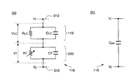
<駆動>
ところで、上述した画素116の1個分は、図14(a)に示されるような等価回路で表すことができる。すなわち、一般的に、i(iは、1≦i≦160を満たす整数)行目の走査線312と、j(jは、1≦j≦120を満たす整数)列目のデータ線212との交差に対応する画素116は、同図に示されるように、抵抗RTおよび容量CTの並列回路で示されるTFD220と、抵抗RLCおよび容量CLCの並列回路で示される液晶容量118との直列回路により表すことができる。
【0053】
ここで、一般的な駆動方法たる4値駆動法(1Hセレクト、1H反転)について説明する。図15は、この4値駆動法(1Hセレクト、1H反転)において、i行j列の画素116に印加される走査信号Yiとデータ信号Xjとの波形例を示す図である。
【0054】
この駆動法では、走査信号Yiとして、1水平走査期間(1H)に選択電圧+VSを印加した後、非選択(保持)期間に非選択電圧+VD/2を印加するとともに、前回の選択から1垂直走査期間(1F)経過すると、今度は選択電圧−VSを印加して、非選択期間に非選択電圧−VD/2を印加する、という動作を繰り返す一方、データ信号Xjとして電圧±VD/2のいずれかを印加する、というものである。
【0055】
この際、ある走査線312への走査信号Yiとして選択電圧+VSを印加すると、その次行に位置する走査線312への走査信号Yi+1として選択電圧−VSを印加する、というように1水平走査期間(1H)毎に選択電圧の極性が反転される動作も行われる。
【0056】
一方、データ信号Xjの電圧は、選択電圧+VSを印加する場合であって、画素116を、ノーマリーホワイトモードにおいて黒色表示とするときには−VD/2となり、画素116を白色表示とするときには+VD/2となる。また、選択電圧−VSを印加する場合であって、画素116を黒色表示とするときには+VD/2となり、画素116を白色表示とするときには−VD/2となる。
【0057】
ところで、この4値駆動法(1Hセレクト、1H反転)では、例えば図16に示されるように、表示画面100aの一部領域Aにおいて、1行毎の白色および黒色からなるゼブラ表示とし、それ以外の領域では単なる例えば白色表示とする場合に、クロストークが発生する、という問題、すなわち濃淡差を伴う白色表示が、領域Aに対してY方向に発生する、という問題が知られている。
【0058】
この発生原因を簡単に説明すれば次のような理由による。
【0059】
まず、画素116の等価回路は、図14(a)で示される通りである。すなわち、非選択期間においてTFD220はオフになるから、その抵抗RTは十分に大きくなり、また、液晶容量118の抵抗RLCは、TFD220のオンオフにかかわらず十分に大きい。このため、非選択期間(保持期間)における画素116の等価回路では、これらの抵抗を無視して、容量CTおよび容量CLCの直列接続回路と表すことができる。このため、容量CLCの両端には、容量CTおよび容量CLCの容量比で決まる電圧が印加されることになる。
【0060】
次に、非選択期間での走査線の電圧(非選択電圧)は一定であるが、データ線の電圧は一般的には電圧±VD/2の両方間で変化する。このため、容量CLCについてみれば、容量CTおよび容量CLCの容量比で決まる電圧変化の影響を受ける。例えば、電圧変化が正方向の場合、容量CLCが走査線Yi側を基準にして正に充電されていると、容量CLCに印加される電圧の絶対値は大きくなり、容量CLCが負に充電されていると、容量CLCに印加される電圧の絶対値は小さくなる。
【0061】
ここで、図16に戻り、領域Aにおいてゼブラ表示を行うと、領域Aにかかるデータ線へのデータ信号においては、電圧±VD/2の切替周期が走査信号の反転周期と一致してしまうので、そのデータ信号は、領域Aにかかる走査線が選択される期間にわたって、電圧±VD/2のいずれか一方に固定されてしまう。これを、領域Aに対してY方向に隣接する領域の画素からみれば、保持期間のうち、領域Aに対応するデータ信号が供給される特定期間において、電圧±VD/2のいずれか一方に固定されることを意味する。
【0062】
そして、相隣接する走査線での選択電圧は、上述したように互いに反対極性であり、容量CLCが充電される極性も反対極性となる。よって、データ信号の電圧が一方に固定されると、その固定された期間中、印加される電圧の絶対値が大きくなった容量CLCの行と、小さくなった容量CLCの行とが交互に現れることになる。
【0063】
したがって、領域Aに対しY方向に隣接する領域の画素に印加される電圧実効値は、奇数行と偶数行とにおいて互いに異なってしまう。この結果、領域Aに対してY方向に隣接する領域において、奇数行の画素116と偶数行の画素116とにおいて濃度差が生じて、上述したようなクロストークが発生してしまうのである。なお、このようなクロストークは、ゼブラ表示のほか、市松模様を表示させる場合にも同様な理由によって発生する。
【0064】
そこで、このクロストークを解消するために、4値駆動法(1/2Hセレクト、1H反転)という駆動方法が用いられる。この駆動法は、図17に示されるように、4値駆動法(1Hセレクト、1H反転)における1水平走査期間(1H)を2分割して前半期間と後半期間とに分け、このうちの一方の期間、例えば後半期間1/2Hにおいて走査線に選択電圧を印加するとともに、1水平走査期間1Hにわたって、データ信号に電圧−VD/2と+VD/2とを印加する期間の割合をそれぞれ50%としたものである。この4値駆動法(1/2Hセレクト、1H反転)によれば、いかなるパターンを表示させたとしても、データ信号Xjにおいて、電圧−VD/2が印加される期間と電圧+VD/2が印加される期間とが互いに半分ずつとなるので、上述したクロストークの発生が防止されることとなる。
【0065】
しかしながら、この4値駆動法(1/2Hセレクト、1H反転)いう駆動方法では、特に階調表示を行うと、データ信号Xjの電圧切替頻度が高くなる、という問題がある。例えば、j列目のデータ線212に供給されるデータ信号Xjの電圧は、図17に示されるように、中間階調(灰色)とすべき画素が列方向に連続していると、走査線312を1本選択する毎(1水平走査期間毎)に3回の割合にて切り替わる。
【0066】
ここで、データ信号Xjの電圧切替頻度が高くなることに伴う問題について説明するため、1垂直走査期間(1F)の大部分を占める非選択期間に着目する。この非選択期間では、TFD220がオフになるから、その抵抗RT(図14(a)参照)は十分に大きくなる。また、液晶容量118の抵抗RLCは、TFD220のオンオフにかかわらず十分に大きい。このため、保持期間における画素116の等価回路は、図18(a)または同図(b)に示されるように、容量CTおよび容量CLCの直列合成容量からなる容量Cpixで表すことができる。なお、容量Cpixは、(CT・CLC)/(CT+CLC)である。
【0067】
次に、図18(a)に示されるように、例えばi行目の走査線312が非選択であって、当該走査線への走査信号Yiが例えば非選択電圧+VD/2に保持されている場合に、j列目のデータ線212へのデータ信号Xjの電圧が+VD/2である状態とする。この状態から、データ信号Xjの電圧が、図18(b)に示されるように−VD/2に切り替わると、1つの画素116にCpix・VDの電荷が供給される。したがって、非選択期間においてデータ信号Xjに電圧切替が発生すると、j列目のデータ線212に接続されるほぼすべての画素116の容量Cpixにわたって、充電または放電が行われることになる(選択走査線との交差に対応する画素は除かれる)。なお、ここでは、画素116における容量Cpixについて説明したが、データ線には、このほかにも種々の容量が寄生する。例えば、図3および図4に示されるように、各走査線312と各データ線212とは、液晶160等を挟んで互いに交差対向しているため、液晶160等を誘電体とする寄生容量を形成する。
【0068】
このため、データ信号Xjの電圧切替頻度が高いと、容量Cpixとともに種々の寄生容量においてそれだけ頻繁に充放電が行われて、電力が消費されてしまうので、低消費電力を阻害する大きな要因となる。
【0069】
そこで、本実施形態に係る表示装置は、クロストークの発生を抑えた上で、データ信号Xjの電圧切替頻度を少なくするため、1水平走査期間を前半期間と後半期間とに分割することをやめて、1水平走査期間の全域にわたって選択電圧を印加する方式を採用するが、第1に、複数本の走査線をまとめてブロック化し、第2に、同一ブロックにあっては、選択電圧の極性を、走査線を1本選択する毎に反転する一方、あるブロックにあって最後に選択される走査線の選択電圧と、次のブロックにあって最初に選択される走査線の選択電圧との極性を同一とする構成とした。ここで、説明の便宜上、本実施形態にあっては、1ブロックを構成する走査線数を「4」として、走査信号やデータ信号を供給するための回路について説明する。
【0070】
<制御回路>
まず、図1における制御回路400によって生成される制御信号やクロック信号などの各種信号のうち、Y(垂直走査)側に用いられる信号について説明する。
【0071】
第1に、スタートパルスDYは、図6に示されるように、1垂直走査期間(1F)の最初に出力されるパルスである。
【0072】
第2に、クロック信号YCKは、Y側の基準信号であり、同図に示されるように、1水平走査期間(1H)の周期を有する。
【0073】
第3に、極性指示信号POLは、走査信号における選択電圧の極性を指示するための信号であり、図8に示されるテーブルにしたがって出力されて、図6に示されるような論理レベルをとる。詳細には、極性指示信号POLにあって、1ブロックを構成する4本の走査線が選択される4水平走査期間(ブロック期間)では、1水平走査期間(1H)毎に論理レベルが反転し、次のブロック期間において最初の1水平走査期間での論理レベルは、直前ブロックにおいて最後の1水平走査期間での論理レベルと同一となっている。さらに、極性指示信号POLでは、交流駆動化のために、ある垂直走査期間(フレーム)と、その直前・直後の垂直走査期間とにおいても、論理レベルが反転した関係となっている。なお、図6において「+」は、正極の選択電圧を印加することを意味し、「−」は、負極の選択電圧を印加することを意味する。
【0074】
次に、X(水平走査)側に用いられる信号について説明する。
【0075】
第1に、スタートパルスDXは、図10に示されるように、1行分の階調データDpixの供給開始タイミングにおいて出力されるパルスである。ここで、階調データDpixは、画素の階調を指示するデータであり、本実施形態では、便宜上、3ビットする。したがって、本実施形態に係る表示装置は、3ビットの階調データDpixにしたがって8(=23)階調の濃淡表示を画素毎に行うものとなる。
【0076】
第2に、クロック信号XCKは、X側の基準信号であり、その周期は、同図に示されるように、階調データDpixの1画素分が供給される期間に相当している。
【0077】
第3に、ラッチパルスLPは、1水平走査期間(1H)の開始時に立ち上がるパルスであって、図10に示されるように、1行分の階調データDpixが供給された後のタイミングにて出力されるパルスである。
【0078】
第4に、階調コードパルスGCPは、図11に示されるように、1水平走査期間(1H)において、中間階調に応じた期間の位置にそれぞれ配列するパルスである。ここで、本実施形態において、3ビットの階調データDpixが、(000)であれば白色表示を指示する一方、(111)であれば黒色表示を指示するものとすると、階調コードパルスGCPは、1水平走査期間(1H)において、白色または黒色を除く灰色の(110)、(101)、(100)、(011)、(010)、(001)の6個に対応してパルスを配列したものとなっている。なお、図11において、階調コードパルスGCPは、実際には、画素の印加電圧−濃度特性(V−I特性)を考慮して設定される。
【0079】
<Yドライバ>
次に、Yドライバ350の詳細について説明する。図5は、このYドライバ350の構成を示すブロック図である。この図において、シフトレジスタ352は、走査線312に総数に対応した160ビットシフトレジスタである。
【0080】
詳細には、シフトレジスタ352は、1垂直走査期間の最初に供給されるスタートパルスDYをクロック信号YCKにしたがって順次シフトして、転送信号YS1、YS2、YS3、…、YS160として順次出力するものである。ここで、転送信号YS1、YS2、YS3、…、YS160は、それぞれ1行目、2行目、3行目、…、160行目の走査線312にそれぞれ1対1に対応するものであって、いずれかの転送信号がHレベルになると、それに対応する走査線312を選択すべきであることを意味する。
【0081】
次に、転送信号YS1、YS2、YS3、…、YS160は、それぞれ各行に対応して設けられたAND回路353の一端に供給されている。一方、各行のAND回路353の他端には、制御信号INHの反転信号が共通に供給されている。ただし、本実施形態において制御信号INHは、常時Lレベルであるので、各行のAND回路353の出力は、それぞれ転送信号YS1、YS2、YS3、…、YS160、そのままとなる。なお、制御信号INHを用いる構成については、後述の応用例において説明することにする。
【0082】
続いて、電圧選択信号形成回路354は、転送信号YS1、YS2、YS3、…、YS160のほか、極性指示信号POLから、走査線312に印加すべき電圧を定める電圧選択信号a、b、c、dのいずれかを、走査線312毎に出力するものである。
【0083】
ここで、本実施形態において、走査線312に印加される走査信号の電圧は、上述したように+VS(正極側選択電圧)、+VD/2(正極側非選択電圧)、−VS(負極側非選択電圧)、−VD/2(負極側選択電圧)の4値であり、このうち、非選択電圧は、選択電圧+VSが印加された後では+VD/2であり、選択電圧−VSが印加された後では−VD/2であって、直前の選択電圧により一義的に定まっている。
【0084】
このため、電圧選択信号形成回路354は、走査信号の電圧レベルが次の関係になるように、1本の走査線において、電圧選択信号a、b、c、dのいずれかを出力する。すなわち、転送信号Ys1、Ys2、…、Ys160のいずれかHレベルになって、それに対応する走査線312を選択すべき水平走査期間である旨が指示されると、電圧選択信号形成回路354は、当該走査線312への走査信号の電圧レベルを、第1に、極性指示信号POLの信号レベルに対応した極性の選択電圧とし、第2に、当該転送信号がLレベルに遷移すると、当該選択電圧に対応する非選択電圧となるように電圧選択信号を生成する。
【0085】
具体的には、電圧選択信号形成回路354は、転送信号がHレベルになったときに、極性指示信号POLがHレベルであれば、当該転送信号に対応する行であって、正極側選択電圧+VSを選択させる電圧選択信号aを当該期間に出力し、この後、当該転送信号がLレベルになれば、正極側非選択電圧+VD/2を選択させる電圧選択信号bを出力する一方、転送信号がHレベルになったときに、極性指示信号POLがLレベルであれば、当該転送信号に対応する行であって、負極側選択電圧−VSを選択させる電圧選択信号cを当該期間に出力し、この後、当該転送信号がLレベルになれば、負極側非選択電圧−VD/2を選択させる電圧選択信号dを出力することになる。
【0086】
次に、レベルシフタ356は、電圧選択信号形成回路354によって出力される電圧選択信号a、b、c、dの電圧振幅をそれぞれ拡大するものである。
【0087】
そして、セレクタ358は、電圧振幅が拡大された電圧選択信号a’、b’、c’、d’によって指示される電圧を、実際に選択して、対応する走査線312の各々に走査信号として印加するものである。
【0088】
<走査信号の電圧波形>
次に、走査信号の電圧波形を説明するために、Yドライバ350の動作について検討する。
【0089】
まず、図6に示されるように、1垂直走査期間(1F)のはじめに、スタートパルスDYが供給されると、当該スタートパルスDYは、シフトレジスタ352によりクロック信号YCKにしたがって転送される結果、転送信号は、YS1、YS2、YS3、…、YS160の順番にて排他的にHレベルとなる。
【0090】
一方、走査信号の電圧は、上述したように、対応する転送信号がHレベルとなったときにおける極性指示信号POLの論理レベルによって指示される。ここで、一般的にi行目の走査線312について着目すると、当該走査線に供給される走査信号Yiは、転送信号YSiがHレベルになったときに、極性指示信号POLがHレベルであれば、正極側選択電圧+VSとなって、その後、正極側非選択電圧+VD/2に保持される一方、転送信号YSiがHレベルになったときに、極性指示信号POLがLレベルであれば、負極側選択電圧−VSとなって、その後、負極側非選択電圧−VD/2に保持される。
【0091】
さらに、極性指示信号POLは、制御回路400によって図8に示されるようなタイムテーブルにしたがって出力される。このため、各走査信号の電圧波形は、図7に示される通りとなる。
【0092】
すなわち、極性指示信号POLは、1ブロックを構成する4本の走査線312が選択される期間については、1水平走査期間毎にレベル反転するので(図6参照)、走査信号の極性は、1本毎に極性反転されることになる。すなわち、正極側選択電圧または負極側選択電圧が1水平走査期間(1H)毎に交互に選択される。
【0093】
くわえて、極性指示信号POLは、あるブロックにおいて最後に走査線312が選択される期間の論理レベルと、当該ブロックの次のブロックにおいて最初に走査線312が選択される期間の論理レベルとは同一とされる。このため、ブロックの境界に位置する2本の走査線312に供給される選択電圧は、互い同一極性となる。
【0094】
また、同一の走査線312に着目すると、極性指示信号POLの論理レベルは、1垂直走査期間毎に反転するので(図6、図8参照)、ある垂直走査期間において、ある走査線が選択されたときの選択電圧が、例えば正側選択電圧+VSであったとすると、次の垂直走査期間において、当該走査線が選択されたときの選択電圧は、負側選択電圧−VSとなる。
【0095】
<Xドライバ>
次に、Xドライバ250の詳細について説明する。図9は、このXドライバ250の構成を示すブロック図である。この図において、シフトレジスタ25100は、1行分の階調データDpixの供給開始タイミングにおいて出力されるスタートパルスDXを、クロック信号XCKの立ち上がり毎に順次シフトして、サンプリング制御信号Xs1、Xs2、Xs3、…、Xs120として出力するものである。
【0096】
続いて、レジスタ(Reg)2520は、データ線212と1対1に対応して設けられ、クロック信号XCKに同期して供給される3ビット階調データDpixを、サンプリング制御信号の立ち上がりにてサンプリングして、保持するものである。さらに、ラッチ回路(L)2530は、レジスタ2520と1対1に対応して設けられ、対応するレジスタ2520によって保持された階調データDpixを、水平走査期間の開始時に立ち上がるラッチパルスLPによってラッチして出力するものである。
【0097】
一方、カウンタ2540は、ラッチパルスLPの立ち上がりにて、階調データの黒色表示に相当する(111)を初期値としてセットするとともに、該初期値を階調コードパルスGCPが立ち上がる毎にダウンカウントして、その計数結果Cを出力するものである。
【0098】
次に、コンパレータ(CMP)2550は、ラッチ回路2530と1対1に対応して設けられ、カウンタ2540による計数結果Cと、対応するラッチ回路2530によりラッチされた階調データDpixとを比較して、後者が前者以上となったときに、Hレベルとなる信号を出力するものである。
【0099】
また、スイッチ2560は、極性指示信号POLがHレベルであれば、図において実線で示される位置をとって、データ電圧+VD/2を電圧供給線2562に、データ電圧−VD/2を電圧供給線2564に、それぞれ供給する一方、極性指示信号POLがLレベルであれば、図において破線で示される位置をとって、データ電圧+VD/2を電圧供給線2564に、データ電圧−VD/2を電圧供給線2562に、それぞれ供給するものである。
【0100】
そして、スイッチ2570は、コンパレータ2550と1対1に対応して、すなわち、データ線212と1対1に対応して設けられるものである。詳細には、スイッチ2570は、コンパレータ2550による比較結果を示す信号がLレベルであれば、図において実線で示されるように電圧供給線2562を選択する一方、該信号がHレベルであれば、図において破線で示されるように電圧供給線2564を選択して、それぞれ選択した電圧供給線に供給されているデータ電圧を、データ信号として、対応するデータ線212に印加するものである。
【0101】
<データ信号の電圧波形>
次に、データ信号の電圧波形を説明するために、Xドライバ350の動作について検討する。
【0102】
まず、図10に示されるように、スタートパルスDXがHレベルに立ち上がると、いずれかの行における1列目、2列目、3列目、…、120列目の画素に対応する階調データDpixが順番に供給される。
【0103】
このうち、1列目の画素に対応する階調データDpixが供給されるタイミングにおいて、シフトレジスタ2510から出力されるサンプリング制御信号Xs1がHレベルに立ち上がると、当該階調データが、1列目に対応するレジスタ2520によってサンプリングされる。
【0104】
次に、2列目の画素に対応する階調データDpixが供給されるタイミングにおいて、サンプリング制御信号Xs2がHレベルに立ち上がると、当該階調データが、2列目に対応するレジスタ2520によってサンプリングされる。以下同様にして、3列目、4列目、…、120列目の画素に対応する階調データDpixの各々が、それぞれ3列目、4列目、…、120列目に対応するレジスタ2520によってサンプリングされることになる。
【0105】
続いて、ラッチパルスLPが出力されると(その論理レベルがHレベルに立ち上がると)、それぞれ各列のレジスタ2520によってサンプリングされた階調データDpixが、それぞれの列に対応するラッチ回路2530によって一斉にラッチされる。そして、このようにラッチされた階調データDpixと、カウンタ2540による計数結果Cとが、コンパレータ2550によってそれぞれ比較されることになる。
【0106】
一方、計数結果Cは、図11に示されるように、ラッチパルスLPの立ち上がりによってセットされた(111)を、階調コードパルスGCPが立ち上がる毎に、カウンタ2550によってダウンカウントした値となる。
【0107】
ここで、一般的にj列目のラッチ回路2530によってラッチされた階調データDpixが、白色に相当する(000)である場合を想定する。この場合、ラッチパルスLPが出力されてから階調コードパルスGCPが6回出力されても、計数結果Cが、ラッチされた(000)以下にならないので、j列目のコンパレータ2550による出力信号は、当該ラッチパルスLPによって規定される1水平走査期間にわたってLレベルを維持する。このため、j列目のスイッチ2570では、電圧供給線2562の選択が維持される。
【0108】
そして、当該水平走査期間において極性指示信号POLがHレベルであれば、スイッチ2560によって電圧+VD/2が電圧供給線2562に供給されるので、データ信号Xjは、図11に示されるように、該水平走査期間にわたって電圧+VD/2のままとなる。
【0109】
反対に、当該水平走査期間において極性指示信号POLがLレベルであれば、スイッチ2560によって電圧−VD/2が電圧供給線2562に供給されるので、データ信号Xjは、同図に示されるように、該水平走査期間にわたって電圧−VD/2のままとなる。
【0110】
次に、一般的にj列目のラッチ回路2530によってラッチされた階調データDpixが、例えば灰色に相当する(100)である場合を想定する。この場合、ラッチパルスLPが出力されてから階調コードパルスGCPが3回出力された時点にて、計数結果Cが、ラッチされた(100)以下になるので、当該時点にて、j列目のコンパレータ2550による出力信号は、LレベルからHレベルに遷移する。このため、j列目のスイッチ2570における選択は、当該時点にて、電圧供給線2562から電圧供給線2564に選択が切り替わる。
【0111】
そして、当該水平走査期間において極性指示信号POLがHレベルであれば、スイッチ2560によって、電圧+VD/2が電圧供給線2562に、電圧−VD/2が電圧供給線2564に、それぞれ供給されるので、データ信号Xjは、図11に示されるように、当該時点にて電圧+VD/2から電圧−VD/2に切り替わる。
【0112】
反対に、当該水平走査期間において極性指示信号POLがLレベルであれば、スイッチ2560によって、電圧−VD/2が電圧供給線2562に、電圧+VD/2が電圧供給線2564に、それぞれ供給されるので、データ信号Xjは、同図に示されるように、当該時点にて電圧−VD/2から電圧+VD/2に切り替わる。
【0113】
なお、ラッチされた階調データDpixが、(100)以外の灰色に相当する場合でも、コンパレータ2550による出力信号の遷移タイミングが異なる点を除いて、同様となる。
【0114】
さらに、一般的にj列目のラッチ回路2530によってラッチされた階調データDpixが、黒色に相当する(111)である場合を想定する。この場合、ラッチパルスLPが出力された時点にて、直ちに、計数結果Cがラッチされた(111)以下になるので、j列目のコンパレータ2550による出力信号は、当該ラッチパルスLPによって規定される1水平走査期間にわたってHレベルを維持する。このため、j列目のスイッチ2570では、電圧供給線2564の選択が維持される。
【0115】
そして、当該水平走査期間において極性指示信号POLがHレベルであれば、スイッチ2560によって電圧−VD/2が電圧供給線2564に供給されるので、データ信号Xjは、図11に示されるように、該水平走査期間にわたって電圧−VD/2のままとなる。
【0116】
反対に、当該水平走査期間において極性指示信号POLがLレベルであれば、スイッチ2560によって電圧+VD/2が電圧供給線2562に供給されるので、データ信号Xjは、同図に示されるように、該水平走査期間にわたって電圧+VD/2のままとなる。
【0117】
したがって、ラッチ回路2530によってラッチされた階調データDpixが同一である場合に、極性指示信号POLがHレベルである場合におけるデータ信号Xjと、極性指示信号POLがLレベルである場合におけるデータ信号Xjとは、データ電圧±VD/2の中心電圧(極性の基準電圧)に対して、互いに反転した関係になる。
【0118】
<データ電圧の切替頻度の低減、クロストークの抑制>
ここで、本実施形態に係る表示装置において、上述したようにブロック化された走査線に走査信号を供給したときに、データ電圧の切替頻度が低減される点と、上述したクロストークが抑制される点とについて、図12を参照して説明する。図12は、本実施形態において、同一ブロックに属するi行目から(i+3)行目までの走査線312、および、当該ブロックの次のブロックにおいて最初に選択される(i+4)行目の走査線312に供給される走査信号、並びに、データ信号との電圧波形を一般的に示す図である。
【0119】
この図に示されるように、一般的にj列目において灰色画素(白または黒以外の画素)が連続する場合に、4本の走査線312を選択するのに要する4水平走査期間において、当該データ線212に供給されるデータ信号Xjの電圧切替回数は10回であり、これを1本の走査線312を選択するのに要する1水平走査期間当たりで換算すると、1.25回である。したがって、本実施形態では、図17に示される4値駆動法(1/2Hセレクト、1H反転)の3回と比較して大幅に低減されるので、その分、低消費電力化が可能となる。
【0120】
さらに、j列目において、白画素および黒画素が交互に配列するパターンを表示する場合、図15に示される4値駆動法(1Hセレクト、1H反転)では、選択電圧の極性に応じて、データ信号Xjが電圧+VD/2または−VD/2の一方に寄ってしまう。そして、これが図16に示されるクロストークの原因となるのは、上述した通りである。
【0121】
これに対し、j列目において白画素および黒画素が交互に配列するパターンを表示する場合であっても、本実施形態では、図12に示されるように、データ信号Xjが電圧+VD/2となる期間と、電圧−VD/2となる期間とが半分ずつとなるので、図17に示される4値駆動法(1/2Hセレクト、1H反転)と同様に、クロストークの発生が防止されることとなる。
【0122】
<連続選択走査線数>
上述した実施形態では、連続して選択する走査線の本数を、便宜上「4」にしたが、本発明は、これに限られない。ここで、連続して選択する走査線の本数を「k」とすると、データ信号の電圧切替回数は、1水平走査期間(1本の走査線の選択)当たりに換算すると、(k+1)/k(回)と表すことができる。このため、図13に示されるように、連続選択走査線kを大きく設定するにつれて、データ信号の電圧切替頻度を、低減させることが可能となる。
【0123】
ここで、上述した4値駆動法(1/2Hセレクト、1H反転)において、中間階調の表示を行うときのデータ信号の電圧切替頻度は3回であるので(図17参照)、本実施形態では、例えば、連続選択走査線kを「10」以上に設定すると、データ信号の電圧切替頻度を、4値駆動法(1/2Hセレクト、1H反転)の約36.7%まで減少させることが可能となる。
【0124】
<実施形態の応用等>
本発明は、上述した実施形態に限られず、次のような種々の応用や変形が可能である。
【0125】
<ブロックを構成する走査線数の変更>
ブロックを構成する走査線数を「4」とした実施形態によれば、列方向に白画素と黒画素とが交互に配列するパターンであっても、データ信号が電圧+VD/2となる期間と、電圧−VD/2となる期間とが半分ずつとなるので、クロストークの発生が防止されることになった。
【0126】
しかしながら、実施形態にあっては、選択電圧の極性に対応した画素が列方向に配列すると、データ信号が電圧+VD/2または−VD/2の一方に寄ってしまう傾向がある。例えば、実施例において、j列目の画素が黒白黒白、白黒白黒、…、という繰り返しパターンになると、対応するデータ線212に供給すべきデータ信号は、図12に示されるように、電圧+VD/2または−VD/2の一方に寄ってしまう。このため、図15に示される4値駆動法(1Hセレクト、1H反転)と同様に、クロストークの発生してしまうことになる。
【0127】
そこで、このようにデータ信号の電圧が寄ってしまうのを防止するためには、ブロックを構成する走査線数をブロック毎に異ならせれば良い、と考える。例えば、図19に示されるように、ブロックを構成する走査線数を上から順に「5」、「4」、「7」とすれば、データ信号の電圧が寄ってしまうパターンの出現率が低下するので、それだけクロストークの発生が抑制されることになる。もちろん、ブロックを構成する走査線数については、「5」、「4」、「7」に限られず、これよりも少数または多数としても良いし、ランダム化しても良い。さらに、ブロックの境界に位置する画素に対して、次に述べるような補正を実行する構成としても良い。
【0128】
<データ信号の補正、選択電圧の補正等>
上述した実施形態によれば、同一ブロック内では選択電圧の極性が1本の走査線312毎に反転されるが、あるブロックの最後に選択される走査線312と、次のブロックの最初に選択される走査線312とに供給される選択電圧は同一極性となるので、他の部分とは異なってしまう。このため、走査線312等の配線抵抗・容量等に起因した波形の鈍化や電界等の相違により、ブロックの境界に沿って(ブロックの端部に位置する走査線312に沿って)、スジ状のムラが発生する場合がある。例えば一面にわたって同一階調(特に中間階調)の表示を行う場合に、ブロックの最初に選択される走査線312に位置する画素は、他の部分と比較して、やや明るくなることが、本件発明者によって確認されている。ここで、画素が明るくなるということは、ノーマリーホワイトモードであれば、液晶容量118に印加される電圧実効値が、本来的な値よりも小さくなってしまうことを意味する。
【0129】
そこで、このブロックの境界においては、次に述べるように、データ信号の補正や、走査信号の補正を単独で、または、適宜組み合わせて実行することが好ましい、と考える。
【0130】
まず、データ信号を補正する構成としては、ブロックの最後に選択される走査線312に位置する画素、または、ブロックの最初に選択される走査線312に位置する画素の少なくとも一方の階調データを、ある値に相当する分だけ一律に加減算して、当該加減算された階調データを、Xドライバ250に供給する構成が考えられる。例えば、上述したようにブロックの最初に選択される走査線312に位置する画素が他の部分と比較して明るくなるのであれば、ブロックの最初に選択される走査線312に位置する画素の階調データについては、明るくなる分に相当する量を、補正量として予め加算しておくのである。
【0131】
スジ状のムラが発生するのは、その部分が他の部分と異なる濃度となってしまうからであるが、このような補正によれば、濃度の異なってしまう分が補正量として予め見越して加算(または減算)されるので、ブロックの境界においては結果的に略同一濃度となる。このため、ムラの発生が抑えられることになる。
【0132】
なお、ムラの発生する箇所については、ブロックの最初に選択される走査線312に位置する画素の方が、ブロックの最後に選択される走査線312に位置する画素よりも目立つことが、本件発明者によって確認されている。このため、ブロックの最初に選択される走査線312に位置する画素について、上述した階調データの補正を実行するのが望ましい、と考える。すなわち、図8において斜線が付された走査線312を選択する場合に、対応する階調データを補正する構成が望ましい。なお、図8において、1行目の走査線312には、斜線が付与されていないが、これは、1垂直走査期間の最初に選択されるために、直前に選択される走査線312が存在しないのでムラが発生しない、または、その影響を無視することができる、と考えられるためである。
【0133】
さて、データ信号を補正する構成については、濃度の異なってしまう分を補正量として予め見越して加算(または減算)する構成のほかに、図11に示される階調コードパルスGCPのパルス配列を時間的にシフトさせる構成も考えられる。すなわち、ブロックの最初に選択される走査線312に位置する画素に対してデータ信号を印加する場合には、点灯電圧の印加時間が、他の走査線に位置する同一階調の画素よりも少し長くなるように、階調コードパルスGCPの配列を変更した構成とするのである。
【0134】
一方、走査信号を補正する構成としては、選択電圧それ自体を補正することが考えられる。ただし、選択電圧自体を補正する構成とするのは、駆動電圧形成回路500(図1参照)にて生成すべき電圧数がそれだけ増加するので、構成が複雑化することになる。
【0135】
そこで、1水平走査期間における選択電圧の印加時間について、ブロックの最初に位置する走査線312と、それ以外の走査線312とで異なるように設定すれば良い。具体的には、ノーマリーホワイトモードにおいてブロックの最初に選択される走査線312に位置する画素が他の走査線に位置する画素と比較して明るくなるのであれば、ブロックの最初に選択される走査線312に対しては、当該走査線312が選択される1水平走査期間の全域にわたって選択電圧を印加する一方、それ以外の走査線312に対しては、前縁または後縁において(当該選択期間の途中まで、または、当該選択期間の途中から)選択電圧の替わりに非選択電圧を印加する構成が考えられる。すなわち、ブロックの最初に選択される走査線に選択電圧が印加される時間を相対的に延長して、電圧実効値の不足分を補うのである。
【0136】
このような構成は、図5のYドライバ350に供給する制御信号INHを、ブロックの最初に位置する走査線312を選択する1水平走査期間の途中までHレベルとする、または、途中からHレベルに遷移させることで実現可能である。
【0137】
なお、データ信号を補正するにしても、走査信号を補正するにしても、実際に補正すべき量は、表示装置100の個体差による影響が大きい、と考えられる。このため、補正量については、個々の装置毎に設定すること望ましい。
【0138】
<ブロックのシフト>
さて、ブロックの境界が垂直走査期間(フレーム)に対して同一位置であると、ムラの発生箇所が固定的となり、ムラとして視認されやすくなる。また、ブロックの境界において補正を行う構成にしても、ムラを完全になくすことは困難な場合がある。
【0139】
そこで、ブロックの境界がフレーム毎に異なるようにすれば、たとえムラが発生したとしても、視認されにくくなる。例えば、極性指示信号POLを、図20に示されるテーブルにしたがって出力する構成とすれば、ブロックの境界がフレーム毎に移動する。このため、数フレームを単位としてみれば、肉眼ではムラが平均化されて見えるので、ムラとしては視認されにくくなる。
【0140】
無論、移動方向は、図20にあっては下方向であるが、上方向でも構わない。また、このようにブロックの境界を移動させる構成においても、ブロックの境界において補正を行う構成にしても良いし、ブロックを構成する走査線数を適宜変更した構成としても良い。
【0141】
このうち、前者に係るブロック境界における補正を行う構成においては、選択電圧を印加する替わりに、非選択電圧を供給する構成としても良い。すなわち、あるフレームにおいてムラの発生するような書込を実行しないようにするのである。ブロックの境界はシフトしているので、あるフレームにおいて書込が実行されなくても、次(または前)のフレームにおいて書込を実行すれば、表示にそれほど影響を与えることはないからである。
【0142】
ここで、ブロックの境界をシフトさせる場合であって、ブロックにおいて最初に選択される走査線312に対し、選択電圧の替わりに、非選択電圧を供給する構成について説明する。
【0143】
この構成では、極性指示信号POLは、図21に示されるテーブルにしたがって出力される。なお、このテーブル自体は、図20に示したものと同一である。ただし、ブロックにおいて最初に走査線312が選択されるべき水平走査期間において、詳細には、図21において○印が付されている期間にて、制御回路400は、制御信号INHをHレベルにさせる。
【0144】
制御信号INHがHレベルであれば、AND回路353(図5参照)が閉じるので、転送信号がHレベルになっても、当該転送信号は、電圧形成回路354に供給されない。電圧形成回路354は、上述したように供給される転送信号がHレベルにならないと、それに対応する走査線312を選択すべき水平走査期間である旨を認識しないので、直前フレームにおける非選択電圧を維持するような電圧選択信号bまたはcを出力することになる。
【0145】
したがって、この構成における走査信号は、例えば図23に示されるように、1フレームにあっては、1行目、5行目、9行目、…、の走査線312には、選択電圧が印加されないで、直前の非選択電圧が維持されることになる。また、続く、2フレームにあっては、2行目、6行目、(10行目)、…、の走査線312には、選択電圧が印加されないで、直前の非選択電圧が維持されることになる。
【0146】
よって、この構成において、ムラを発生させるような書込は、そもそも実行されないので、表示品位の低下を抑えることが可能となる。
なお、この例では、ブロックの最初に選択される走査線には選択電圧に替えて非選択電圧を与えているが、ブロックの境界を上方向へシフトさせる場合には、ブロックの最後に選択される走査線には選択電圧に替えて非選択電圧を与えることとなる。
【0147】
ただし、書込を実行しないことに起因するクロストークが発生する可能性があるので、例えば書込をスキップさせてから1フレーム経過した選択時において、詳細には、図24において○印が付されている期間において、データ信号や走査信号を補正して、画素に印加される電圧実効値を、当該クロストークをなくす方向に修正しても良い。なお、補正を行うのは、書込をスキップさせる期間の1フレーム前でも良いが、いずれにしても、書込をスキップする期間と、補正を実行する期間とは、時間的に離れていない方が望ましい、と考える。
【0148】
また、制御回路400が、極性指示信号POLを、図24に示されるテーブルにしたがって出力するとともに、制御信号INHを、同図において○印が付されている期間にてHレベルにさせる構成としても良い。この構成では、ブロックの最後に位置する走査線312が選択される水平走査期間において当該走査線に印加される電圧と、その前行・後行の走査線に印加される電圧とは、いずれも非選択電圧のままとなる。このため、次に選択される次ブロックの最初の走査線に影響を与えるノイズ等が少ない、と考える。
【0149】
よって、この構成においても、ブロック境界のスジ状のムラは小さくなる。なお、選択電圧の印加をスキップすることに対する補正は、スキップさせる期間の1フレーム前または後に行えば良い。
【0150】
また、この例では、ブロックの最後に選択される走査線には、選択電圧に替えて非選択電圧を与えているが、ブロックの境界を上方向へシフトさせる場合には、ブロックの最初に選択される走査線には選択電圧に替えて非選択電圧を与えることとなる。いずれにしても、書込をスキップする期間と、補正を実行する期間とは、時間的に離れていない方が望ましい点は同様である。
【0151】
<選択の順番、飛び越し走査>
また、実施形態にあっては、走査線312を上から順番に1本ずつ選択して選択電圧を供給する構成としたが、選択の順番についてはこれに限られない。例えば、フレームではなく、奇数フィールドと偶数フィールドとに分割し、奇数フィールドについては、例えば奇数行目の走査線312を順番に選択する一方、偶数フィールドについては、例えば偶数行目の走査線312を順番に選択する構成(インタレース)としても良い。このような構成とすれば、1フィールドにおいて選択すべき走査線数が半分になるので、動作周波数が半分で済み、その分、低消費電力化を図ることが可能となる。
【0152】
また、1以上の走査線312おきに飛び越し走査をしても良いし、また、1画面を水平走査方向に沿って複数の領域に分割するとともに、分割領域を順番に選択しつつ、選択した分割領域において例えば上から走査線312を順番に選択しても良い。
【0153】
<実施形態のまとめ>
なお、上述した実施形態では、階調データを3ビットとして、8階調表示をする場合について説明したが、本発明はこれに限られず、単なる1ビットによる階調(オンオフ)データによる2値表示としても良いし、2ビットの階調データによる4階調表示としても良いし、また、4ビット、5ビット、6ビット、…、nビットの階調データによる16、32、64、…、2n階調表示としても良い。さらに、R(赤)、G(緑)、B(青)の3画素で1ドットを構成して、カラー表示を行うとしても良い。
【0154】
さらに、実施形態にあっては、液晶容量の電圧無印加状態において白色表示を行うノーマリーホワイトモードとして説明したが、同状態において黒色表示となるノーマリーブラックモードとしても良い。
【0155】
くわえて、実施形態にあっては、透過型としたが、反射型としても良いし、両者を併用した半透過半反射型としても良い。
【0156】
一方、実施形態におけるXドライバ250は、図9に示されるように、カウンタ2540によるカウンタ結果Cを列毎に共用する構成としたが、列毎にカウンタを設けて、ラッチされた階調データとの大小比較を実行する構成としても良い。
【0157】
また、実施形態にあっては、選択電圧が印加されたときに、黒色表示に寄与する点灯電圧を、時間的に後方に寄せて印加する構成としたが、時間的に前方に印加する構成としても良い。
【0158】
くわえて、実施形態では、画素の表示色と走査線の選択電圧とに応じてデータ電圧±VD/2の印加期間を調整してデータ信号としたが、画素の表示色と走査線の選択電圧とに応じて電圧そのものを規定したデータ信号を供給しても良い。
【0159】
さらに、実施形態にあっては、液晶容量の書込極性を1垂直走査期間毎に反転する構成としたが、これに限られず、例えば2垂直走査期間以上の周期で反転駆動する構成としても良い。
【0160】
また、上述した表示装置100におけるTFD220は、データ線212の側に接続され、液晶容量118が走査線312の側に接続されているが、これとは逆に、TFD220が走査線312の側に、液晶層118がデータ線212の側にそれぞれ接続される構成でも良い。
【0161】
さらに、TFD220は、二端子型スイッチング素子の一例であり、他に、ZnO(酸化亜鉛)バリスタや、MSI(Metal Semi-Insulator)などを用いた素子のほか、これら素子を2つ逆向きに直列接続または並列接続したものなどを、二端子型スイッチング素子として用いることが可能である。
【0162】
また、TFD220などのようなスイッチング素子を用いずに、画素を駆動するパッシブ・マトリクス型の表示装置にも適用可能である。
【0163】
さらに、実施形態にあっては、液晶としてTN型やSTN型とした場合について説明したが、分子の長軸方向と短軸方向とで可視光の吸収に異方性を有する染料(ゲスト)を一定の分子配列の液晶(ホスト)に溶解して、染料分子を液晶分子と平行に配列させたゲストホスト型などの液晶を用いても良い。
【0164】
くわえて、電圧無印加時には液晶分子が両基板に対して垂直方向に配列する一方、電圧印加時には液晶分子が両基板に対して水平方向に配列する、という垂直配向(ホメオトロピック配向)の構成としても良いし、電圧無印加時には液晶分子が両基板に対して水平方向に配列する一方、電圧印加時には液晶分子が両基板に対して垂直方向に配列する、という平行(水平)配向(ホモジニアス配向)の構成としても良い。
【0165】
このように、本発明の駆動方法に適合するものであれば、液晶や配向方式として、種々のものを用いることが可能である。
【0166】
<表示装置の改良構造>
次に、表示品位の一層の向上を意図した表示装置100の改良構造について説明する。上述した実施形態によれば、図16に示したクロストークの発生を抑えつつ、表示装置100の低消費電力化を図ることが可能である。しかしながら、画素電極間の容量結合に起因して、複数本の走査線をまとめたブロックの境界部に、横筋状のむらが表示される可能性がある。そこで、表示装置100自体の構造に改良を施すことで、このような表示むらの発生を抑制する。以下、表示装置100の一部を構成する素子基板200に関して、3つの改良構造を例示する。これらの改良構造に共通することは、隣接した画素電極234の間に、データ線212または導電線280といった導電性を有する導電部を、画素電極234と電気的に分離した状態で介在させている点である。
【0167】
<第1の改良構造>
図28は、第1の改良構造に係る素子基板200の上面図である。同図において、上述した実施形態と同様の部材については、同一の符号を付することにより、詳細な説明を省略する。上述した実施形態と同様、この素子基板200の対向面上には、データ線212とTFD220と画素電極234とが設けられている。
【0168】
この素子基板200の構造上の特徴は、データ線212の一部を「ト」の字状に突出さることにより、データ線212に突出部212aが設けられている点にある。具体的には、突出部212aは、データ線212の延在方向(Y方向)とは異なるX方向(横(右)方向)に突出し、Y方向において隣接した2つの画素電極234の間に介在している。突出部212aおよび画素電極234は、素子基板200の対向面上で両者を離間することにより、或いは、絶縁膜を介して積層することにより、電気的に分離されている。また、突出部212aは、素子基板200上に存在する全ての隣接画素電極間に介在している。あるデータ線212に設けられた突出部212aの先端は、その直右のデータ線212と離間しているため、隣接した左右のデータ線212は、互いに電気的に分離されている。
【0169】
このように、Y方向に隣接する2つの画素電極234の間に突出部212aを入り込ませることで、突出部212aは、隣接した画素電極234の間の寄生容量を低減する静電シールドとして機能する。これにより、ブロック境界部に表示される横筋状のむらを有効に抑制する。
【0170】
まず、横筋状の表示むらの発生メカニズムについて説明する。図29は、突出部212aを設けない構造における画素間の寄生容量モデルを示す図である。同図において、Cmは、画素電極とデータ線との間の寄生容量、Cpは、画素電極と走査線との間の寄生容量、そして、Cppは、隣接した2つの画素電極間の寄生容量である。図29に示したモデルは、図30に示す等価回路で表すことができる。同図において、画素p1には、走査線(図中、コモン1)の電圧とデータ線(図中、セグメント)の電圧とが印加されている。また、画素p1とX方向に隣接した画素p2には、コモン1とは異なる走査線(図中、コモン2)の電圧とデータ線(セグメント)の電圧とが印加されている。
【0171】
一般に、一方の画素電極の電圧VbがΔVbだけ変化した場合、これと隣接した他方の画素電極の電圧Vaの変化量ΔVaは、(Vpp/(Cm+Cp+Cpp))・ΔVbとして表される。コモン1上の画素p1の書き込みが終了した時点における画素電圧を−Vp1とし、コモン2上の画素p2書き込みが終了した状態を考える。まず、画素p1と画素p2との書込極性が逆の場合(逆極性書込)、書き込みの前後で、画素p2の画素電圧は−Vp2からVp2へと変化し、その保持電圧はVhld/2から−Vhld/2へと変化する(図31参照)。
【0172】
これを図30に示した一方の画素電極の電圧Vbの変化とみなすと、(Vhld/2−Vp2)から(Vp2−Vhld/2)への変化となり、ΔVbは(2Vp2−Vhld)となる。したがって、2Vp2<Vhldの場合には、ΔVaは負側に変化するため、画素p1の画素電圧の絶対値が増す(表示が暗くなる)。
【0173】
一方、画素p1と画素p2との書込極性が同一の場合(同極性書込)、書き込みの前後で、画素p2の画素電圧は、Vp2から−Vp2へと変化し、その保持電圧は、−Vhld/2からVhld/2へと変化する(図32参照)。
【0174】
これを図30に示した一方の画素電極の電圧Vbの変化とみなすと、(Vhld/2−Vp2)から(Vp2−Vhld/2)への変化となり、ΔVbは(Vhld−2Vp2)となる。したがって、2Vp2<Vhldの場合には、ΔVaは正側に変化するため、画素p1の画素電圧の絶対値が減る(表示が明るくなる)。
【0175】
画素電圧が1V(off)〜3V(on)程度で、保持電圧Vhldが4V程度を想定した場合、ΔVbは、±2・|Vp2−Vhld|=±2Vとなる。また、(Cpp/(Cm+Cp+Cpp))を0.01程度と仮定した場合、逆極性書込と同極性書込とでは、実効電圧に40mv(20mv×2)の差が生じて、表示むらが発生する。このことは、ある書込行の画素の濃さは、次の行の書込行の書込極性によって異なってしまうことを意味する。本実施形態に係る駆動方式によれば、同一のブロック内では常に逆極性になり、ブロック境界部では同一極性になる。その結果、ブロック境界部において、横筋むらが発生する。
【0176】
これに対して、データ線212に突出部212aを設けた場合、隣接した2つの画素の等価回路は、図33に示すようになる。それぞれの画素電極234と突出部212aとの間に寄生容量Cpcが新たに形成される。この寄生容量Cpcを設けることで、隣接した画素電極234の間の寄生容量Cppが低減する。これにより、(Cpp/(Cm+Cp+Cpp))の値も十分に小さくなるので、一方の画素電極234の電圧変化に起因した他方の画素電極234の電圧変動が緩和される。つまり、突出部212aは、寄生容量Cppに起因した画素電極の電圧変動を緩和する静電シールドとして機能する。その結果、駆動回路による補正を行わなくても、ブロック境界部における横筋むらの発生を有効に低減できる。
【0177】
<第2の改良構造>
図34は、第2の改良構造に係る素子基板200の上面図である。この素子基板200の構造上の特徴は、データ線212の一部を略十字状に突出させることにより、データ線212に突出部212b,212cが設けられている点にある。具体的には、右突出部212bは右側に向かって突出しており、左突出部212cは左側に向かって突出している。これらの突出部212b,212cは、第1の改良構造と同様に、Y方向に隣接した2つの画素電極234の間に介在しており、画素電極234と電気的に分離されている。また、突出部212b,212cの少なくとも一方は、素子基板200上に存在する全ての隣接画素電極間に介在している。あるデータ線212に設けられた右突出部212bの先端は、その直右のデータ線212に設けられた左突出部212cの先端と離間しているため、隣接した上下のデータ線212は、互いに電気的に分離されている。
【0178】
このような構成によれば、突出部212b,212cと画素電極234と間に寄生容量Cpcが形成されるので、突出部212a,212bが静電シールドとして機能する。その結果、第1の改良構造と同様に、寄生容量Cppに起因した隣接する画素電極234の電圧変動が小さくなる。その結果、駆動回路による補正を行わなくても、ブロック境界部における横筋むらの発生を有効に低減できる。
【0179】
<第3の改良構造>
図35は、第3の改良構造に係る素子基板200の上面図である。この素子基板200の構造上の特徴は、複数の導電線280がデータ線212とは別部材で設けられている点にある。具体的には、それぞれの導電線280は、データ線212とは異なる方向に延在しており、かつ、データ線212とは絶縁膜を介して電気的に分離されている。それぞれの導電線280は、Y方向に隣接する2つの画素電極234の間に介在している。また、複数の導電線280は、図35の左端で共通接続されている。導電線280の材料としては、酸化インジウムまたは酸化錫等の透明な導電材料を用いることが好ましい。これにより、表示が暗くなるのを防止する。
【0180】
このような構成によれば、導電線280と画素電極234と間に新たに寄生容量Cpcが形成される。したがって、それぞれの導電線280が静電シールドとして機能するため、駆動回路による補正を行わなくても、ブロック境界部における横筋むらの発生を有効に低減できる。なお、導電線280にはある電圧(一定電圧である必要はない)が常時印加されることが好ましいが、多数の導電線280が共通接続された構造(容量結合の影響を受け難い構造)では、導電線280はフローティングであってもよい。
【0181】
<電子機器>
次に、上述した実施形態に係る表示装置を電子機器に用いた例について説明する。
【0182】
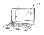
<その1:モバイル型パーソナルコンピュータ>
まず、上述した表示装置100を、パーソナルコンピュータの表示部に適用した例について説明する。図25は、このパーソナルコンピュータの構成を示す斜視図である。
【0183】
図において、コンピュータ1100は、キーボード1102を備えた本体部1104と、表示部として用いられる表示装置100とを備えている。なお、表示装置100として透過型液晶装置を用いる場合には、暗所での視認性を確保するため、背面にバックライト(図示省略)が設けられる。
【0184】
<その2:携帯電話>
さらに、上述した表示装置100を、携帯電話の表示部に適用した例について説明する。図26は、この携帯電話の構成を示す斜視図である。
【0185】
図において、携帯電話1200は、複数の操作ボタン1202のほか、受話口1204、送話口1206とともに、上述した表示装置100を備えるものである。なお、表示装置100として、液晶装置を用いる場合には、暗所での視認性を確保するため、透過型や半透過半反射型であれば、バックライトが、反射型であればフロントライト(いずれも図示省略)が、それぞれ設けられる。
【0186】
<その3:ディジタルスチルカメラ>
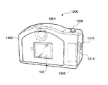
次に、上述した表示装置を、ファインダに用いたディジタルスチルカメラについて説明する。
【0187】
図27は、このディジタルスチルカメラの背面を示す斜視図である。通常の銀塩カメラは、被写体の光像によってフィルムを感光させるのに対し、ディジタルスチルカメラ1300は、被写体の光像をCCD(Charge Coupled Device)などの撮像素子により光電変換して撮像信号を生成するものである。ここで、ディジタルスチルカメラ1300におけるケース1302の背面には、上述した表示装置100が設けられ、CCDによる撮像信号に基づいて、表示を行う構成となっている。このため、表示装置100は、被写体を表示するファインダとして機能することになる。また、ケース1302の前面側(図28においては裏面側)には、光学レンズやCCDなどを含んだ受光ユニット1304が設けられている。
【0188】
ここで、撮影者が表示装置100に表示された被写体像を確認して、シャッタボタン1306を押下すると、その時点におけるCCDの撮像信号が、回路基板1308のメモリに転送・格納される。
【0189】
また、このディジタルスチルカメラ1300にあっては、ケース1302の側面には、外部表示を行うために、ビデオ信号出力端子1312と、データ通信用の入出力端子1314とが設けられている。
【0190】
なお、電子機器としては、図25のパーソナルコンピュータや、図26の携帯電話、図27のディジタルスチルカメラの他にも、液晶テレビや、ビューファインダ型、モニタ直視型のビデオテープレコーダ、カーナビゲーション装置、ページャ、電子手帳、電卓、ワードプロセッサ、ワークステーション、テレビ電話、POS端末、タッチパネルを備えた機器等などが挙げられる。そして、これらの各種電子機器の表示部として、上述した表示装置が適用可能なのは言うまでもない。
【0191】
【発明の効果】
以上説明したように本発明によれば、表示示品位の低下を抑えつつ、低消費電力化を図ることが可能となる。
【図面の簡単な説明】
【図1】 本発明の実施形態に係る表示装置の電気的な構成を示すブロック図である。
【図2】 同表示装置の構成を示す斜視図である。
【図3】 同表示装置をX方向で破断した場合の構成を示す部分断面図である。
【図4】 同表示装置の要部構成を示す部分破断斜視図である。
【図5】 同表示装置におけるYドライバの構成を示すブロック図である。
【図6】 同Yドライバの動作を説明するためのタイミングチャートである。
【図7】 同Yドライバによる走査信号の電圧波形を説明するための図である。
【図8】 同表示装置において、各行に印加される選択電圧の極性を示すタイムテーブルである。
【図9】 同表示装置におけるXドライバの構成を示すブロック図である。
【図10】 同Xドライバの動作を説明するためのタイミングチャートである。
【図11】 同Xドライバによるデータ信号の電圧波形を説明するためのタイミングチャートである。
【図12】 同表示装置の画素に印加される電圧波形等を示す図である。
【図13】 走査線を連続して選択する本数と電圧切替回数(消費電力)との関係を示す図である。
【図14】 (a)および(b)は、それぞれ実施形態に係る表示装置における画素の等価回路を示す図である。
【図15】 4値駆動法(1Hセレクト、1H反転)における走査信号Yi、Yi+1およびデータ信号Xjの波形例を示す図である。
【図16】 表示の不具合を説明するための図である。
【図17】 4値駆動法(1/2Hセレクト、1H反転)における走査信号Yi、Yi+1およびデータ信号Xjの波形例を示す図である。
【図18】 (a)、(b)は、それぞれ非選択期間(保持期間)におけるデータ信号Xjの電圧切り替わりによる電力消費を説明するための図である。
【図19】 本発明の応用例に係る表示装置において、各行に印加される選択電圧の極性を示すタイムテーブルである。
【図20】 本発明の応用例に係る表示装置において、各行に印加される選択電圧の極性を示すタイムテーブルである。
【図21】 本発明の応用例に係る表示装置において、各行に印加される選択電圧の極性等を示すタイムテーブルである。
【図22】 同表示装置において、制御信号INH等を示すタイミングチャートである。
【図23】 同表示装置における走査信号の電圧波形を説明するための図である。
【図24】 本発明の応用例に係る表示装置において、各行に印加される選択電圧の極性等を示すタイムテーブルである。
【図25】 実施形態に係る表示装置を適用した電子機器の一例たるパーソナルコンピュータの構成を示す斜視図である。
【図26】 同表示装置を適用した電子機器の一例たる携帯電話の構成を示す斜視図である。
【図27】 同表示装置を適用した電子機器の一例たるディジタルスチルカメラの背面構成を示す斜視図である。
【図28】 第1の改良構造に係る素子基板の上面図である。
【図29】 突出部を設けない構造における画素間の寄生容量モデルの図である。
【図30】 突出部を設けない構造における隣接した二画素の等価回路を示す図である。
【図31】 画素電圧および保持電圧の電圧変化を示す図である。
【図32】 画素電極および保持電圧の電圧変化を示す図である。
【図33】 突出部を設けた構造における隣接した二画素の等価回路を示す図である。
【図34】 第2の改良構造に係る素子基板の上面図である。
【図35】 第3の改良構造に係る素子基板の上面図である。
【符号の説明】
100 表示装置
105 液晶
116 画素
118 液晶
200 素子基板
212 データ線
212a 突出部
212b 上突出部
212c 下突出部
220 TFD
234 画素電極
250 Xドライバ(データ線駆動回路)
280 導電線
300 対向基板
312 走査線
350 Yドライバ(走査線駆動回路)
1100 パーソナルコンピュータ
1200 携帯電話
1300 ディジタルスチルカメラ
2540 カウンタ
2550 コンパレータ[0001]
BACKGROUND OF THE INVENTION
The present invention relates to a display device, a driving circuit thereof, a driving method thereof, and an electronic apparatus which achieve low power consumption while suppressing deterioration in display quality in a configuration in which pixels are switched by a thin film diode, for example.
[0002]
[Prior art]
In recent years, display devices using electro-optic changes in liquid crystals have been used in various electronic devices and televisions as display devices that replace cathode ray tubes (CRTs) by taking advantage of their thinness, small size, and low power consumption. Widely used.
[0003]
This display device can be roughly classified into an active matrix type in which pixels are driven by switching and a passive matrix type in which pixels are driven without using a switching element. Among these, the active matrix type according to the former further includes a type using a three-terminal type switching element such as a thin film transistor (TFT) and a thin film diode (TFD) depending on the type of the switching element. The type using the two-terminal switching element can be roughly divided into two types, but the latter type using the two-terminal switching element has a principle of short circuit failure between wirings because there is no wiring intersection. In that the film formation process and the photolithography process can be shortened, and further, it is advantageous in terms of low power consumption.
[0004]
On the other hand, in a display device in which pixels are switched by a two-terminal switching element, there are various modes for reducing display quality. However, the quaternary driving method (1 / 2H) in which the ratio of the period during which two voltages that can be taken by the data line (segment electrode) are finally applied becomes half of any pattern displayed. It is known that such a decrease in display quality is eliminated by adopting (select, 1H inversion).
[0005]
By the way, especially in portable electronic devices such as PDAs (Personal Digital Assistants) and mobile phones, battery driving is a principle, so there is a strong demand for low power consumption. For this reason, display devices applied to portable electronic devices are also strongly required to have low power consumption.
[0006]
Furthermore, in recent years, various functions such as music playback have been added to this type of portable electronic device, and the power consumption of the display device can be compared to generate power allocated to these new functions. There is even a demand to reduce even 1 mW.
[0007]
On the other hand, in recent years, display devices are required to have not only simple black-and-white display but also high gradation display that performs display with rich intermediate gradation.
[0008]
[Problems to be solved by the invention]
However, in the above four-value driving method, when halftone display is performed, the voltage switching frequency of the data line is increased, so that there is a disadvantage that power is wasted due to the capacity associated with the data line. On the other hand, if the quaternary driving method (1 / 2H select, 1H inversion) is not adopted, there is a problem that the display quality deteriorates depending on the mode.
[0009]
The present invention has been made in view of the above-described circumstances, and an object of the present invention is to provide a display device capable of reducing power consumption while suppressing deterioration in display display quality, a drive circuit thereof, To provide a driving method and an electronic apparatus.
[0010]
[Means for Solving the Problems]
In order to achieve the above object, a driving circuit for a display device according to an embodiment of the present invention is a driving circuit for a display device that drives a pixel provided corresponding to an intersection of a scanning line and a data line, A scanning line driving circuit that selects one scanning line at a time and applies a selection voltage to the selected scanning line while applying a non-selection voltage to the other scanning lines. A plurality of the scanning lines are grouped into blocks, and the polarity of the selection voltage is set to one of the scanning lines with reference to an intermediate value between the on voltage and the off voltage applied to the data line in the blocked block. It is inverted every time it is selected, and the polarity of the selection voltage of the scanning line selected last in the block is the same as the selection voltage of the scanning line selected first in the next block of the block. Scan line When the scanning line is selected and a selection voltage is applied to the dynamic circuit and the data line, the content to be displayed in the pixel corresponding to the intersection of the scanning line and the data line and the selection voltage A data line driving circuit that applies an on voltage or an off voltage according to the polarity is characterized.
[0011]
According to this configuration, even when a lit pixel and a non-lit pixel appear alternately in one data line, the voltage effective value applied to the data line and the voltage effective value applied to the other data line Since the difference from the value is reduced, the deterioration of display quality can be suppressed. Further, even when intermediate grayscale pixels continue in one data line, the frequency of switching the data voltage applied to the data line is reduced, so that the capacity associated with the data line and its drive circuit is charged. The power consumed unnecessarily by the discharge is suppressed, and the power consumption can be reduced accordingly.
[0012]
The lighting voltage in this case refers to a data signal voltage having a polarity opposite to the selection voltage applied during a period when a certain scanning line is selected, and is not lit. The voltage is a data signal voltage having the same polarity as the selection voltage applied during a period in which a certain one scanning line is selected.
[0013]
According to this configuration, even when a lit pixel and a non-lit pixel appear alternately in one data line, there is no bias in the effective voltage value of the data line, but there is a bias depending on the display pattern. There is a time to do. For example, if display is performed such that lighted pixels and non-lighted pixels are arranged in accordance with the polarity of the selection voltage in the block, the voltage effective value of the data line is biased.
[0014]
Therefore, in the above configuration, it is preferable that the number of scanning lines constituting the block is different from the number of scanning lines constituting the block next to the block. With such a configuration, the appearance rate of the pattern causing the bias is lowered, so that the deterioration of display quality can be further suppressed.
[0015]
Further, in the above driving circuit, the scanning line corresponding to the boundary of the block has the same polarity of the selection voltage as the other parts, so that a difference in display is likely to occur. Therefore, in the above configuration, the data line driving circuit is selected when a selection voltage is applied to the first selected scanning line in the block, or selected in the last selected scanning line in the block. The display difference can be reduced by correcting the on-voltage or the off-voltage at least when one of the voltages is applied.
[0016]
In order to reduce such a display difference, correction on the scanning line driving circuit side can be performed in addition to correction on the data line driving circuit side. That is, the scanning line driving circuit applies a selection voltage to the first selected scanning line in one block, or applies a selection voltage to the last selected scanning line in one block. A configuration in which the selection voltage or the selection voltage application time is corrected in at least one of the applied times is preferable. According to this configuration, the difference in display can be reduced by correcting the selection voltage itself or the time for applying the selection time.
[0017]
On the other hand, it is preferable that the scanning line driving circuit is configured to block the scanning lines so that the boundaries of the blocks are sequentially shifted every vertical scanning period. According to this configuration, since the boundary portion of the block moves with time, even if a display difference occurs in the portion, it becomes inconspicuous, and as a result, it is difficult to be visually recognized as a deterioration in display quality.
[0018]
In such a configuration in which the block boundaries are sequentially shifted, the scanning line driving circuit applies the non-selection voltage instead of the selection voltage to the first or last selected scanning line in one block. May be. In this way, writing at the boundary portion of the block is skipped, so that occurrence of a display difference can be suppressed.
[0019]
In addition, the data line driving circuit may display the display difference even when the on voltage or the off voltage is corrected when a selection voltage is applied to the first or last selected scanning line in the block. Can be suppressed.
[0020]
Alternatively, when the selection voltage is applied to the first selected scanning line in one block, or when the selection voltage is applied to the last selected scanning line in one block. Even if the selection voltage or the selection voltage application time is corrected at least when it is applied, occurrence of a display difference can be similarly suppressed.
[0021]
Here, the present invention can also be realized as a driving method of a display device. That is, this driving method is a driving method of a display device that drives pixels provided corresponding to the intersection of a scanning line and a data line, and selects the scanning line one by one and selects the selected scanning line. While a selection voltage is applied to a line, a non-selection voltage is applied to the other scanning lines to the scanning line, and a plurality of the scanning lines are blocked together, and the block is divided into blocks. The polarity of the selection voltage is inverted every time one of the scanning lines is selected with reference to an intermediate value between the on-voltage and the off-voltage applied to the data line, and is selected last in the block. The selection voltage of the scanning line to be selected is the same as the selection voltage of the first scanning line in the block next to the block, and the selection voltage is applied to the data line. When It features a method of applying an on-voltage or OFF voltage depending on the polarity of the content and the selected voltage to be displayed in the pixel corresponding to the intersection between the scanning lines and the data lines.
[0022]
According to this method, the difference between the voltage effective value applied to one data line and the voltage effective value applied to another data line is small, and the switching frequency of the data voltage applied to the data line is small. Is also low. For this reason, it is possible to reduce power consumption while suppressing deterioration of display quality.
[0023]
In order to achieve the above object, a display device according to the present invention includes a pixel provided corresponding to an intersection of a scan line and a data line, and selects the scan line one by one. A scanning line driving circuit that applies a selection voltage to the selected scanning line while applying a non-selection voltage to the other scanning lines to the scanning line. In the block, the polarity of the selection voltage is inverted every time one of the scanning lines is selected with reference to the intermediate value between the on voltage and the off voltage applied to the data line. And a scanning line driving circuit in which the selection voltage of the scanning line selected last in the block and the selection voltage of the scanning line first selected in the next block of the block have the same polarity, For data line When the scanning line is selected and a selection voltage is applied, an on voltage or an off voltage is selected depending on the content to be displayed in the pixel corresponding to the intersection of the scanning line and the data line and the polarity of the selection voltage. The data line driving circuit for applying a voltage is provided.
[0024]
According to this display device, similarly to the above drive circuit, the difference between the effective voltage value applied to one data line and the effective voltage value applied to the other data line is small, and The switching frequency of the applied data voltage is also low. For this reason, it is possible to reduce power consumption while suppressing deterioration of display quality.
[0025]
Here, the display device according to the present invention includes a plurality of scanning lines, a plurality of data lines, and a plurality of pixels provided corresponding to the intersections of the scanning lines and the data lines. Includes a pixel electrode, and a two-terminal switching element provided between the pixel electrode and the data line, and is electrically connected to the pixel electrode between adjacent pixel electrodes in the extending direction of the data line. It is preferable to interpose a separated conductive part.
[0026]
According to this display device, since the conductive portion interposed between adjacent pixel electrodes functions as an electrostatic shield that reduces the parasitic capacitance between these pixel electrodes, occurrence of display unevenness at the block boundary portion is suppressed. . The conductive portion may be a protruding portion in which a part of the data line is protruded in a direction different from the extending direction of the data line. In addition, when a plurality of conductive lines extending in a direction different from the extending direction of the data lines and electrically connected to each other are provided while being electrically separated from the data lines, Each corresponds to a conductive portion.
[0027]
In the display device according to the present invention, the pixel includes a two-terminal switching element having one end connected to either the scanning line or the data line, and the other of the scanning line or the data line. A configuration including an electro-optic capacitance in which an electro-optic material is sandwiched between a pixel electrode connected to the other end of the two-terminal switching element is preferable. When two-terminal switching elements are used in this way, short-circuit defects between wires do not occur in principle and the manufacturing process is simplified compared to a configuration using three-terminal switching elements. It is advantageous.
[0028]
Furthermore, such a two-terminal switching element preferably has a structure having a conductor / insulator / conductor structure. In this configuration, any conductor can be used as it is as a scanning line or a data line, and the insulator can be formed by oxidizing the conductor itself.
[0029]
In addition, since the electronic device according to the present invention includes the display device, it is possible to reduce power consumption and the like while suppressing deterioration in display quality. Examples of such electronic devices include personal computers, mobile phones, digital still cameras, and the like.
[0030]
DETAILED DESCRIPTION OF THE INVENTION
Hereinafter, embodiments of the present invention will be described with reference to the drawings.
[0031]
<Configuration>
First, the electrical configuration of the display device according to the embodiment of the present invention will be described. FIG. 1 is a block diagram showing this configuration.
[0032]
As shown in this figure, in the
[0033]
In this embodiment, for convenience of explanation, the total number of
[0034]
Next, the
[0035]
The
[0036]
On the other hand, the
[0037]
Here, in this embodiment, the voltage ± V S Is used as the selection voltage in the scanning signal and the voltage ± V D / 2 is configured to be shared by the non-selection voltage in the scanning signal and the data voltage in the data signal. Note that the non-selection voltage and the data voltage may be different from each other, but may be different from each other, but the configuration is complicated by the increase in the number of voltages to be generated by the drive
[0038]
In this embodiment, the polarity reference of the voltage applied to the
[0039]
<Mechanical configuration>
Next, a mechanical configuration of the display device according to the present embodiment will be described. FIG. 2 is a perspective view showing the entire configuration of the
[0040]
As shown in these drawings, in the
[0041]
In addition to the
[0042]
On the other hand, a
[0043]
Further, on the opposing surface of the
[0044]
Next, the outside of the display area will be described. As shown in FIG. 2, an
[0045]
In addition, an FPC (Flexible Printed Circuit)
[0046]
Note that, unlike FIG. 2, the
[0047]
<Pixel configuration>
Next, a detailed configuration of the
[0048]
Now, as shown in FIG. 4,
[0049]
Note that a transparent
[0050]
On the other hand, on the opposing surface of the opposing
[0051]
In such a configuration, when a selection voltage for turning on the
Here, since the alignment state of the
[0052]
<Drive>
Incidentally, one
[0053]
Here, a four-value driving method (1H selection, 1H inversion), which is a general driving method, will be described. FIG. 15 is a diagram showing waveform examples of the scanning signal Yi and the data signal Xj applied to the
[0054]
In this driving method, as the scanning signal Yi, the selection voltage + V is applied in one horizontal scanning period (1H). S After the voltage is applied, the non-selection voltage + V D / 2 is applied, and when one vertical scanning period (1F) elapses from the previous selection, this time, the selection voltage −V S Is applied to the non-selection voltage −V during the non-selection period. D / 2 is applied repeatedly while the voltage ± V is used as the data signal Xj. D / 2 is applied.
[0055]
At this time, as a scanning signal Yi to a
[0056]
On the other hand, the voltage of the data signal Xj is selected voltage + V S When the
[0057]
By the way, in this quaternary driving method (1H select, 1H inversion), for example, as shown in FIG. 16, in a partial area A of the
[0058]
The cause for this will be briefly explained as follows.
[0059]
First, an equivalent circuit of the
[0060]
Next, the voltage of the scanning line (non-selection voltage) in the non-selection period is constant, but the voltage of the data line is generally voltage ± V D / 2 varies between both. For this reason, the capacity C LC As for the capacity C T And capacity C LC It is affected by the voltage change determined by the capacitance ratio. For example, when the voltage change is in the positive direction, the capacitance C LC Is positively charged with reference to the scanning line Yi side, the capacitance C LC The absolute value of the voltage applied to the capacitor increases and the capacitance C LC Is negatively charged, the capacity C LC The absolute value of the voltage applied to becomes small.
[0061]
Here, returning to FIG. 16, when zebra display is performed in the region A, the voltage ± V is applied to the data signal to the data line applied to the region A. D Since the switching cycle of / 2 coincides with the inversion cycle of the scanning signal, the data signal has a voltage ± V over the period when the scanning line over the region A is selected. D / 2 will be fixed. If this is viewed from the pixel in the region adjacent to the region A in the Y direction, the voltage ± V in the specific period in which the data signal corresponding to the region A is supplied in the holding period. D It means that it is fixed to either one of / 2.
[0062]
The selection voltages in the adjacent scanning lines have opposite polarities as described above, and the capacitance C LC The polarity charged is also the opposite polarity. Therefore, when the voltage of the data signal is fixed to one side, the capacitance C in which the absolute value of the applied voltage is increased during the fixed period. LC And the reduced capacity C LC Will appear alternately.
[0063]
Therefore, the effective voltage values applied to the pixels in the region adjacent to the region A in the Y direction are different from each other in the odd and even rows. As a result, in the region adjacent to the region A in the Y direction, density differences occur between the odd-numbered
[0064]
Therefore, in order to eliminate this crosstalk, a driving method called a four-value driving method (1 / 2H select, 1H inversion) is used. In this driving method, as shown in FIG. 17, one horizontal scanning period (1H) in the four-value driving method (1H select, 1H inversion) is divided into two parts, ie, the first half period and the second half period. For example, in the latter
[0065]
However, this four-value driving method (1 / 2H select, 1H inversion) has a problem that the frequency of switching the voltage of the data signal Xj increases particularly when gradation display is performed. For example, as shown in FIG. 17, the voltage of the data signal Xj supplied to the
[0066]
Here, in order to explain a problem associated with an increase in the frequency of voltage switching of the data signal Xj, attention is paid to a non-selection period that occupies most of one vertical scanning period (1F). In this non-selection period, since the
[0067]
Next, as shown in FIG. 18A, for example, the
[0068]
For this reason, if the voltage switching frequency of the data signal Xj is high, the capacitance C pix At the same time, charging and discharging are frequently performed in various parasitic capacitances, and power is consumed, which is a major factor that hinders low power consumption.
[0069]
Therefore, the display device according to the present embodiment stops dividing one horizontal scanning period into the first half period and the second half period in order to reduce the voltage switching frequency of the data signal Xj while suppressing the occurrence of crosstalk. A method of applying a selection voltage over the entire area of one horizontal scanning period is employed. First, a plurality of scanning lines are grouped into blocks, and secondly, the polarity of the selection voltage is set in the same block. Each time one scanning line is selected, the polarity is inverted, while the polarity of the selection voltage of the scanning line selected last in a block and the selection voltage of the scanning line selected first in the next block Are the same. Here, for convenience of explanation, in the present embodiment, a circuit for supplying a scanning signal and a data signal with the number of scanning lines constituting one block being “4” will be described.
[0070]
<Control circuit>
First, signals used on the Y (vertical scanning) side among various signals such as a control signal and a clock signal generated by the
[0071]
First, the start pulse DY is a pulse output at the beginning of one vertical scanning period (1F), as shown in FIG.
[0072]
Second, the clock signal YCK is a Y-side reference signal and has a period of one horizontal scanning period (1H) as shown in FIG.
[0073]
Third, the polarity instruction signal POL is a signal for instructing the polarity of the selection voltage in the scanning signal, and is output according to the table shown in FIG. 8 and has a logic level as shown in FIG. Specifically, in the polarity instruction signal POL, the logic level is inverted every horizontal scanning period (1H) in four horizontal scanning periods (block periods) in which four scanning lines constituting one block are selected. In the next block period, the logic level in the first one horizontal scanning period is the same as the logic level in the last one horizontal scanning period in the immediately preceding block. Further, in the polarity instruction signal POL, the logic level is inverted in a certain vertical scanning period (frame) and the vertical scanning period immediately before and immediately after it for AC driving. In FIG. 6, “+” means that a positive selection voltage is applied, and “−” means that a negative selection voltage is applied.
[0074]
Next, signals used on the X (horizontal scanning) side will be described.
[0075]
First, the start pulse DX is a pulse output at the supply start timing of the gradation data Dpix for one row as shown in FIG. Here, the gradation data Dpix is data instructing the gradation of the pixel, and in this embodiment, 3 bits are used for convenience. Therefore, the display device according to the present embodiment has 8 (= 2) according to the 3-bit gradation data Dpix. Three ) Gray scale display is performed for each pixel.
[0076]
Secondly, the clock signal XCK is a reference signal on the X side, and its period corresponds to a period during which one pixel of the gradation data Dpix is supplied, as shown in FIG.
[0077]
Third, the latch pulse LP is a pulse that rises at the start of one horizontal scanning period (1H), and as shown in FIG. 10, at the timing after the gradation data Dpix for one row is supplied. This is the output pulse.
[0078]
Fourthly, as shown in FIG. 11, the gradation code pulse GCP is a pulse arranged at a position corresponding to an intermediate gradation in one horizontal scanning period (1H). Here, in this embodiment, if the 3-bit gradation data Dpix is (000), white display is instructed, while if it is (111), black display is instructed, the gradation code pulse GCP In one horizontal scanning period (1H), pulses corresponding to six gray (110), (101), (100), (011), (010), and (001) other than white or black are excluded. It is an array. In FIG. 11, the gradation code pulse GCP is actually set in consideration of the applied voltage-density characteristic (VI characteristic) of the pixel.
[0079]
<Y driver>
Next, details of the
[0080]
Specifically, the
[0081]
Next, the transfer signals YS1, YS2, YS3,..., YS160 are respectively supplied to one end of an AND
[0082]
Subsequently, the voltage selection
[0083]
Here, in this embodiment, the voltage of the scanning signal applied to the
[0084]
For this reason, the voltage selection
[0085]
Specifically, the voltage selection
[0086]
Next, the
[0087]
Then, the
[0088]
<Voltage waveform of scanning signal>
Next, in order to describe the voltage waveform of the scanning signal, the operation of the
[0089]
First, as shown in FIG. 6, when the start pulse DY is supplied at the beginning of one vertical scanning period (1F), the start pulse DY is transferred according to the clock signal YCK by the
[0090]
On the other hand, as described above, the voltage of the scanning signal is indicated by the logic level of the polarity indication signal POL when the corresponding transfer signal becomes H level. Here, in general, focusing on the i-
[0091]
Further, the polarity instruction signal POL is output by the
[0092]
That is, since the polarity instructing signal POL is inverted every horizontal scanning period during the period in which the four
[0093]
In addition, the polarity indication signal POL has the same logic level as the period when the
[0094]
Further, when paying attention to the
[0095]
<X driver>
Next, details of the
[0096]
Subsequently, the register (Reg) 2520 is provided in one-to-one correspondence with the
[0097]
On the other hand, the
[0098]
Next, the comparator (CMP) 2550 is provided in one-to-one correspondence with the
[0099]
Further, the
[0100]
The
[0101]
<Voltage waveform of data signal>
Next, in order to describe the voltage waveform of the data signal, the operation of the
[0102]
First, as shown in FIG. 10, when the start pulse DX rises to the H level, the gradation data corresponding to the pixels in the first, second, third,..., 120th column in any row. Dpix is supplied in order.
[0103]
Among these, when the sampling control signal Xs1 output from the
[0104]
Next, when the gradation control signal Xs2 rises to the H level at the timing when the gradation data Dpix corresponding to the pixel in the second column is supplied, the gradation data is sampled by the
[0105]
Subsequently, when the latch pulse LP is output (when the logic level rises to H level), the gradation data Dpix sampled by the
[0106]
On the other hand, as shown in FIG. 11, the count result C is a value obtained by down-counting (111) set by the rising edge of the latch pulse LP by the
[0107]
Here, it is generally assumed that the gradation data Dpix latched by the
[0108]
If the polarity instruction signal POL is at the H level in the horizontal scanning period, the voltage + V is switched by the
[0109]
On the other hand, if the polarity instruction signal POL is at the L level during the horizontal scanning period, the voltage −V D / 2 is supplied to the
[0110]
Next, it is assumed that the gradation data Dpix latched by the
[0111]
If the polarity instruction signal POL is at the H level in the horizontal scanning period, the voltage + V is switched by the
[0112]
On the other hand, if the polarity instruction signal POL is at the L level in the horizontal scanning period, the
[0113]
Even when the latched gradation data Dpix corresponds to a gray color other than (100), the same applies except that the transition timing of the output signal by the
[0114]
Further, it is assumed that the gradation data Dpix latched by the
[0115]
If the polarity instruction signal POL is at the H level during the horizontal scanning period, the
[0116]
On the contrary, if the polarity instruction signal POL is at L level in the horizontal scanning period, the voltage + V is switched by the
[0117]
Therefore, when the gradation data Dpix latched by the
[0118]
<Reduction of data voltage switching frequency and suppression of crosstalk>
Here, in the display device according to the present embodiment, when the scanning signal is supplied to the scanning lines blocked as described above, the frequency of switching the data voltage is reduced, and the above-described crosstalk is suppressed. This point will be described with reference to FIG. FIG. 12 shows the
[0119]
As shown in this figure, in general, when gray pixels (pixels other than white or black) are continuous in the j-th column, in the four horizontal scanning periods required to select four
[0120]
Further, when displaying a pattern in which white pixels and black pixels are alternately arranged in the j-th column, in the four-value driving method (1H select, 1H inversion) shown in FIG. 15, data is displayed according to the polarity of the selected voltage. Signal Xj is voltage + V D / 2 or -V D It will be close to one of / 2. This causes the crosstalk shown in FIG. 16 as described above.
[0121]
On the other hand, even when displaying a pattern in which white pixels and black pixels are alternately arranged in the j-th column, in this embodiment, as shown in FIG. 12, the data signal Xj is a voltage + V. D / 2 and voltage -V D Since the period of / 2 is halved, the occurrence of crosstalk is prevented as in the four-value driving method (1 / 2H selection, 1H inversion) shown in FIG.
[0122]
<Number of continuously selected scanning lines>
In the embodiment described above, the number of scanning lines to be continuously selected is set to “4” for convenience, but the present invention is not limited to this. Here, if the number of scanning lines to be continuously selected is “k”, the voltage switching number of the data signal is (k + 1) / k when converted per one horizontal scanning period (selection of one scanning line). (Times). For this reason, as shown in FIG. 13, as the continuously selected scanning line k is set larger, the voltage switching frequency of the data signal can be reduced.
[0123]
Here, in the above-described quaternary driving method (1 / 2H selection, 1H inversion), the voltage switching frequency of the data signal when displaying the intermediate gradation is 3 times (see FIG. 17). For example, when the continuous selection scanning line k is set to “10” or more, the voltage switching frequency of the data signal can be reduced to about 36.7% of the four-value driving method (1 / 2H selection, 1H inversion). It becomes possible.
[0124]
<Application of the embodiment>
The present invention is not limited to the above-described embodiments, and various applications and modifications are possible as follows.
[0125]
<Change in the number of scanning lines constituting a block>
According to the embodiment in which the number of scanning lines constituting the block is “4”, even if the pattern is a pattern in which white pixels and black pixels are alternately arranged in the column direction, the data signal is a voltage + V. D / 2 and voltage -V D Since the period of ½ is halved, the occurrence of crosstalk is prevented.
[0126]
However, in the embodiment, when the pixels corresponding to the polarity of the selection voltage are arranged in the column direction, the data signal is the voltage + V. D / 2 or -V D There is a tendency to approach one side of / 2. For example, in the embodiment, when the pixel in the j-th column has a repetitive pattern of black / black / white / white / black / white,..., The data signal to be supplied to the corresponding
[0127]
Therefore, in order to prevent the voltage of the data signal from deviating in this way, it is considered that the number of scanning lines constituting the block may be different for each block. For example, as shown in FIG. 19, when the number of scanning lines constituting a block is “5”, “4”, and “7” in order from the top, the appearance rate of the pattern in which the voltage of the data signal is shifted decreases. Therefore, the occurrence of crosstalk is suppressed accordingly. Of course, the number of scanning lines constituting the block is not limited to “5”, “4”, and “7”, and may be smaller or larger than this, or may be randomized. Furthermore, it is good also as a structure which performs the following correction | amendment with respect to the pixel located in the boundary of a block.
[0128]
<Data signal correction, selection voltage correction, etc.>
According to the embodiment described above, the polarity of the selection voltage is inverted for each
[0129]
Therefore, at the boundary of this block, it is preferable that the correction of the data signal and the correction of the scanning signal are preferably performed alone or in combination as appropriate, as described below.
[0130]
First, as a configuration for correcting the data signal, gradation data of at least one of the pixel located on the
[0131]
The streaky unevenness occurs because the density of the portion differs from that of the other portions. However, according to such correction, the amount of difference in density is added in anticipation as a correction amount in advance. (Or subtraction), resulting in substantially the same density at the block boundary. For this reason, the occurrence of unevenness is suppressed.
[0132]
It should be noted that, regarding the portion where unevenness occurs, the pixel located on the
[0133]
As for the configuration for correcting the data signal, in addition to the configuration for adding (or subtracting) the difference in density in advance as the correction amount, the pulse array of the gradation code pulse GCP shown in FIG. It is also possible to adopt a configuration in which the shift is performed. That is, when a data signal is applied to a pixel located on the
[0134]
On the other hand, as a configuration for correcting the scanning signal, it is conceivable to correct the selection voltage itself. However, the configuration for correcting the selection voltage itself increases the number of voltages to be generated by the drive voltage forming circuit 500 (see FIG. 1), and thus the configuration becomes complicated.
[0135]
Therefore, the application time of the selection voltage in one horizontal scanning period may be set to be different between the
[0136]
In such a configuration, the control signal INH supplied to the
[0137]
Whether the data signal is corrected or the scanning signal is corrected, the amount to be actually corrected is considered to be greatly influenced by individual differences in the
[0138]
<Block shift>
Now, when the block boundary is at the same position with respect to the vertical scanning period (frame), the occurrence of unevenness is fixed and is easily recognized as unevenness. Even if the correction is performed at the block boundary, it may be difficult to completely eliminate the unevenness.
[0139]
Therefore, if the boundaries of the blocks are different for each frame, even if unevenness occurs, it is difficult to visually recognize. For example, if the polarity instruction signal POL is output according to the table shown in FIG. 20, the block boundary moves from frame to frame. Therefore, when several frames are taken as a unit, unevenness appears to be averaged with the naked eye, so that unevenness is less visible.
[0140]
Of course, the moving direction is the downward direction in FIG. 20, but it may be the upward direction. Further, even in the configuration in which the block boundary is moved as described above, the correction may be performed at the block boundary, or the number of scanning lines configuring the block may be appropriately changed.
[0141]
Among these, in the structure which correct | amends in the block boundary which concerns on the former, it is good also as a structure which supplies a non-selection voltage instead of applying a selection voltage. That is, writing that causes unevenness in a certain frame is not executed. This is because, since the block boundary is shifted, even if writing is not executed in a certain frame, if writing is executed in the next (or previous) frame, the display is not significantly affected.
[0142]
Here, a description will be given of a configuration in which a non-selection voltage is supplied instead of a selection voltage to a
[0143]
In this configuration, the polarity instruction signal POL is output according to the table shown in FIG. The table itself is the same as that shown in FIG. However, in the horizontal scanning period in which the
[0144]
If the control signal INH is at the H level, the AND circuit 353 (see FIG. 5) is closed. Therefore, even if the transfer signal becomes the H level, the transfer signal is not supplied to the
[0145]
Therefore, for example, as shown in FIG. 23, the scanning signal in this configuration applies a selection voltage to the
[0146]
Therefore, in this configuration, writing that causes unevenness is not executed in the first place, so that it is possible to suppress deterioration in display quality.
In this example, the non-selection voltage is applied to the scanning line selected at the beginning of the block instead of the selection voltage. However, when the block boundary is shifted upward, the scanning line is selected at the end of the block. A non-selection voltage is applied to the scanning line instead of the selection voltage.
[0147]
However, since there is a possibility that crosstalk occurs due to not executing writing, for example, when one frame has elapsed after skipping writing, a circle mark is attached in FIG. 24 in detail. During this period, the data signal and the scanning signal may be corrected to correct the effective voltage value applied to the pixel in a direction in which the crosstalk is eliminated. The correction may be performed one frame before the period during which writing is skipped, but in any case, the period during which writing is skipped and the period during which correction is performed are not separated in time. Is desirable.
[0148]
In addition, the
[0149]
Therefore, even in this configuration, the stripe-like unevenness at the block boundary is reduced. The correction for skipping the application of the selection voltage may be performed one frame before or after the skip period.
[0150]
In this example, the scanning line selected at the end of the block is given a non-selection voltage instead of the selection voltage. However, if the block boundary is shifted upward, the scanning line is selected at the beginning of the block. A non-selection voltage is applied to the scanning line instead of the selection voltage. In any case, it is desirable that the period during which writing is skipped and the period during which correction is performed should not be separated in time.
[0151]
<Selection order, interlaced scanning>
In the embodiment, the selection voltage is supplied by selecting the
[0152]
Further, interlaced scanning may be performed every one or
[0153]
<Summary of Embodiment>
In the above-described embodiment, the case where the gradation data is 3 bits and the 8 gradation display is performed has been described. However, the present invention is not limited to this, and the binary display based on the gradation (on / off) data by only 1 bit. 4 gradation display using 2 bit gradation data, or 16, 32, 64,..., 2 using 4 bit, 5 bit, 6 bit,..., N bit gradation data. n It is good also as a gradation display. Furthermore, one pixel may be configured by three pixels of R (red), G (green), and B (blue) to perform color display.
[0154]
Furthermore, although the embodiment has been described as a normally white mode in which white display is performed in a state where no voltage is applied to the liquid crystal capacitor, a normally black mode in which black display is performed in the same state may be employed.
[0155]
In addition, although the transmissive type is used in the embodiment, a reflective type may be used, or a semi-transmissive and semi-reflective type using both of them may be used.
[0156]
On the other hand, as shown in FIG. 9, the
[0157]
Further, in the embodiment, when the selection voltage is applied, the lighting voltage that contributes to black display is applied while being moved backward in time, but as the structure that is applied forward in time. Also good.
[0158]
In addition, in the embodiment, according to the display color of the pixel and the selection voltage of the scanning line, the data voltage ± V D Although the data signal is adjusted by adjusting the application period of / 2, a data signal that defines the voltage itself according to the display color of the pixel and the selection voltage of the scanning line may be supplied.
[0159]
Further, in the embodiment, the writing polarity of the liquid crystal capacitor is reversed every vertical scanning period. However, the present invention is not limited to this. For example, the liquid crystal capacitor may be reversed and driven at a cycle of two vertical scanning periods or more. .
[0160]
In addition, the
[0161]
Furthermore, the
[0162]
Further, the present invention can also be applied to a passive matrix display device that drives pixels without using a switching element such as TFD220.
[0163]
Further, in the embodiment, the case where the liquid crystal is a TN type or STN type has been described. However, a dye (guest) having anisotropy in absorption of visible light in the major axis direction and the minor axis direction of the molecule is used. A guest-host type liquid crystal in which dye molecules are aligned in parallel with liquid crystal molecules may be used by dissolving in a liquid crystal (host) having a certain molecular arrangement.
[0164]
In addition, the liquid crystal molecules are aligned vertically with respect to both substrates when no voltage is applied, while the liquid crystal molecules are aligned horizontally with respect to both substrates when voltage is applied. Alternatively, liquid crystal molecules are aligned horizontally with respect to both substrates when no voltage is applied, while liquid crystal molecules are aligned vertically with respect to both substrates when voltage is applied (homogeneous alignment). It is good also as a structure of.
[0165]
As described above, various liquid crystal and alignment methods can be used as long as they are compatible with the driving method of the present invention.
[0166]
<Improved structure of display device>
Next, an improved structure of the
[0167]
<First improved structure>
FIG. 28 is a top view of the
[0168]
The structural feature of the
[0169]
In this manner, the protrusion 212a functions as an electrostatic shield that reduces the parasitic capacitance between the
[0170]
First, the mechanism of occurrence of horizontal stripe-like display unevenness will be described. FIG. 29 is a diagram illustrating a parasitic capacitance model between pixels in a structure in which the protruding portion 212a is not provided. In the figure, Cm is a parasitic capacitance between the pixel electrode and the data line, Cp is a parasitic capacitance between the pixel electrode and the scanning line, and Cpp is a parasitic capacitance between two adjacent pixel electrodes. is there. The model shown in FIG. 29 can be represented by an equivalent circuit shown in FIG. In the figure, the voltage of the scanning line (common 1 in the figure) and the voltage of the data line (segment in the figure) are applied to the pixel p1. Further, the voltage of the scanning line (common 2 in the figure) and the voltage of the data line (segment) different from the common 1 are applied to the pixel p2 adjacent to the pixel p1 in the X direction.
[0171]
In general, when the voltage Vb of one pixel electrode changes by ΔVb, the change amount ΔVa of the voltage Va of the other pixel electrode adjacent thereto is expressed as (Vpp / (Cm + Cp + Cpp)) · ΔVb. Consider a state in which the pixel voltage at the time when the writing of the pixel p1 on the common 1 is finished is −Vp1, and the writing of the pixel p2 on the common 2 is finished. First, when the writing polarities of the pixel p1 and the pixel p2 are opposite (reverse polarity writing), the pixel voltage of the pixel p2 changes from −Vp2 to Vp2 before and after writing, and the holding voltage is Vhld / 2. To -Vhld / 2 (see FIG. 31).
[0172]
Considering this as a change in the voltage Vb of one pixel electrode shown in FIG. 30, the change is from (Vhld / 2−Vp2) to (Vp2−Vhld / 2), and ΔVb is (2Vp2−Vhld). Therefore, when 2Vp2 <Vhld, ΔVa changes to the negative side, so that the absolute value of the pixel voltage of the pixel p1 increases (the display becomes dark).
[0173]
On the other hand, when the pixel p1 and the pixel p2 have the same writing polarity (same polarity writing), the pixel voltage of the pixel p2 changes from Vp2 to −Vp2 before and after writing, and the holding voltage is − It changes from Vhld / 2 to Vhld / 2 (see FIG. 32).
[0174]
Considering this as a change in the voltage Vb of one pixel electrode shown in FIG. 30, the change is from (Vhld / 2−Vp2) to (Vp2−Vhld / 2), and ΔVb is (Vhld−2Vp2). Therefore, when 2Vp2 <Vhld, ΔVa changes to the positive side, so that the absolute value of the pixel voltage of the pixel p1 decreases (the display becomes brighter).
[0175]
When it is assumed that the pixel voltage is about 1 V (off) to 3 V (on) and the holding voltage Vhld is about 4 V, ΔVb is ± 2 · | Vp2−Vhld | = ± 2V. When (Cpp / (Cm + Cp + Cpp)) is assumed to be about 0.01, a difference of 40 mv (20 mv × 2) is generated in the effective voltage between the reverse polarity writing and the same polarity writing, resulting in display unevenness. This means that the pixel density of a certain write line differs depending on the write polarity of the next write line. According to the driving method according to the present embodiment, the polarity is always reversed in the same block, and the polarity is the same at the block boundary. As a result, horizontal stripe unevenness occurs at the block boundary.
[0176]
On the other hand, when the protrusion 212a is provided on the
[0177]
<Second improved structure>
FIG. 34 is a top view of the
[0178]
According to such a configuration, since the parasitic capacitance Cpc is formed between the protrusions 212b and 212c and the
[0179]
<Third improved structure>
FIG. 35 is a top view of the
[0180]
According to such a configuration, a parasitic capacitance Cpc is newly formed between the conductive line 280 and the
[0181]
<Electronic equipment>
Next, an example in which the display device according to the above-described embodiment is used in an electronic device will be described.
[0182]
<Part 1: Mobile personal computer>
First, an example in which the above-described
[0183]
In the figure, a
[0184]
<Part 2: Mobile phone>
Furthermore, an example in which the above-described
[0185]
In the figure, a
[0186]
<3: Digital still camera>
Next, a digital still camera using the above-described display device as a finder will be described.
[0187]
FIG. 27 is a perspective view showing the back of the digital still camera. A normal silver salt camera sensitizes a film with a light image of a subject, whereas a
[0188]
Here, when the photographer confirms the subject image displayed on the
[0189]
In the
[0190]
In addition to the personal computer shown in FIG. 25, the cellular phone shown in FIG. 26, and the digital still camera shown in FIG. , Pagers, electronic notebooks, calculators, word processors, workstations, videophones, POS terminals, devices equipped with touch panels, and the like. And it cannot be overemphasized that the display apparatus mentioned above is applicable as a display part of these various electronic devices.
[0191]
【The invention's effect】
As described above, according to the present invention, it is possible to reduce the power consumption while suppressing the deterioration of the display display quality.
[Brief description of the drawings]
FIG. 1 is a block diagram showing an electrical configuration of a display device according to an embodiment of the present invention.
FIG. 2 is a perspective view showing a configuration of the display device.
FIG. 3 is a partial cross-sectional view showing a configuration when the display device is broken in the X direction.
FIG. 4 is a partially broken perspective view showing the main configuration of the display device.
FIG. 5 is a block diagram showing a configuration of a Y driver in the display device.
FIG. 6 is a timing chart for explaining the operation of the Y driver.
FIG. 7 is a diagram for explaining a voltage waveform of a scanning signal by the Y driver.
FIG. 8 is a time table showing the polarity of a selection voltage applied to each row in the display device.
FIG. 9 is a block diagram showing a configuration of an X driver in the display device.
FIG. 10 is a timing chart for explaining the operation of the X driver.
FIG. 11 is a timing chart for explaining a voltage waveform of a data signal by the X driver.
FIG. 12 is a diagram showing voltage waveforms applied to the pixels of the display device.
FIG. 13 is a diagram showing the relationship between the number of scanning lines to be continuously selected and the number of voltage switching times (power consumption).
FIGS. 14A and 14B are diagrams each showing an equivalent circuit of a pixel in the display device according to the embodiment. FIGS.
FIG. 15 is a diagram showing an example of waveforms of scanning signals Yi, Yi + 1 and a data signal Xj in the four-value driving method (1H select, 1H inversion).
FIG. 16 is a diagram for explaining a display defect.
FIG. 17 is a diagram illustrating an example of waveforms of scanning signals Yi, Yi + 1 and a data signal Xj in a four-value driving method (1 / 2H selection, 1H inversion).
FIGS. 18A and 18B are diagrams for explaining power consumption due to voltage switching of a data signal Xj in a non-selection period (holding period), respectively.
FIG. 19 is a time table showing the polarity of the selection voltage applied to each row in the display device according to the application example of the invention.
FIG. 20 is a time table showing the polarity of the selection voltage applied to each row in the display device according to the application example of the invention.
FIG. 21 is a time table showing the polarity and the like of the selection voltage applied to each row in the display device according to the application example of the invention.
FIG. 22 is a timing chart showing a control signal INH and the like in the display device.
FIG. 23 is a diagram for explaining a voltage waveform of a scanning signal in the display device.
FIG. 24 is a time table showing the polarity and the like of a selection voltage applied to each row in a display device according to an application example of the present invention.
FIG. 25 is a perspective view illustrating a configuration of a personal computer as an example of an electronic apparatus to which the display device according to the embodiment is applied.
FIG. 26 is a perspective view showing a configuration of a mobile phone as an example of an electronic apparatus to which the display device is applied.
FIG. 27 is a perspective view showing a rear configuration of a digital still camera as an example of an electronic apparatus to which the display device is applied.
FIG. 28 is a top view of an element substrate according to a first improved structure.
FIG. 29 is a diagram of a parasitic capacitance model between pixels in a structure in which no protrusion is provided.
FIG. 30 is a diagram illustrating an equivalent circuit of two adjacent pixels in a structure in which no protrusion is provided.
FIG. 31 is a diagram illustrating a change in voltage of a pixel voltage and a holding voltage.
FIG. 32 is a diagram illustrating a voltage change of a pixel electrode and a holding voltage.
FIG. 33 is a diagram showing an equivalent circuit of two adjacent pixels in a structure provided with a protrusion.
FIG. 34 is a top view of an element substrate according to a second improved structure.
FIG. 35 is a top view of an element substrate according to a third improved structure.
[Explanation of symbols]
100 Display device
105 liquid crystal
116 pixels
118 liquid crystal
200 element substrate
212 data lines
212a Protrusion
212b Upper protrusion
212c Lower protrusion
220 TFD
234 Pixel electrode
250 X driver (data line drive circuit)
280 conductive wire
300 Counter substrate
312 scan line
350 Y driver (scan line drive circuit)
1100 Personal computer
1200 mobile phone
1300 Digital still camera
2540 counter
2550 Comparator
Claims (16)
前記走査線を1本ずつ選択して、当該選択した走査線に対して選択電圧を印加する一方、それ以外の走査線に対して非選択電圧を走査線に印加する走査線駆動回路であって、
前記走査線を複数本まとめてブロック化し、当該ブロック化されたブロックにおいて、前記選択電圧の極性を、前記データ線に印加されるオン電圧およびオフ電圧の中間値を基準として走査線の1本選択する毎に反転するとともに、
前記ブロックにあって最後に選択される走査線の選択電圧と当該ブロックの次のブロックにあって最初に選択される走査線の選択電圧との極性を同一とする走査線駆動回路と、
データ線に対し、
前記走査線が選択されて選択電圧が印加されたときに、当該走査線と当該データ線との交差に対応する画素にて表示すべき内容と当該選択電圧の極性とに応じてオン電圧またはオフ電圧を印加するデータ線駆動回路と
を具備することを特徴とする表示装置の駆動回路。A driving circuit of a display device for driving a pixel provided corresponding to an intersection of a scanning line and a data line,
A scanning line driving circuit that selects one scanning line at a time and applies a selection voltage to the selected scanning line while applying a non-selection voltage to the other scanning lines. ,
A plurality of the scanning lines are grouped together, and the polarity of the selection voltage is selected in the blocked block based on an intermediate value between the on voltage and the off voltage applied to the data line. Every time you turn it over,
A scanning line driving circuit in which the polarity of the selection voltage of the scanning line selected last in the block and the selection voltage of the scanning line selected first in the next block of the block are the same;
For data lines
When the scanning line is selected and a selection voltage is applied, an on voltage or an off voltage is selected depending on the content to be displayed in the pixel corresponding to the intersection of the scanning line and the data line and the polarity of the selection voltage. And a data line driving circuit for applying a voltage. A driving circuit for a display device.
ことを特徴とする請求項1に記載の表示装置の駆動回路。The drive circuit of the display device according to claim 1, wherein the number of scanning lines constituting the block is different from the number of scanning lines constituting the block next to the block.
前記ブロックにあって最初に選択された走査線に選択電圧が印加されたとき、または、前記ブロックにあって最後に選択された走査線に選択電圧が印加されたときの少なくとも一方において、
前記オン電圧または前記オフ電圧を補正する
ことを特徴とする請求項1に記載の表示装置の駆動回路。The data line driving circuit includes:
At least one of when the selection voltage is applied to the first selected scanning line in the block or when the selection voltage is applied to the last selected scanning line in the block,
The drive circuit of the display device according to claim 1, wherein the on voltage or the off voltage is corrected.
前記ブロックにあって最初に選択された走査線に選択電圧が印加されたとき、または、前記ブロックにあって最後に選択された走査線に選択電圧が印加されたときの少なくとも一方において、
当該選択電圧または当該選択電圧印加時間を補正する
ことを特徴とする請求項1に記載の表示装置の駆動回路。The scanning line driving circuit includes:
At least one of when the selection voltage is applied to the first selected scanning line in the block or when the selection voltage is applied to the last selected scanning line in the block,
The display device driving circuit according to claim 1, wherein the selection voltage or the selection voltage application time is corrected.
前記ブロックの境界が垂直走査期間毎に順次シフトするように、前記走査線のブロック化を実行する
ことを特徴とする請求項1に記載の表示装置の駆動回路。The scanning line driving circuit includes:
The display device driving circuit according to claim 1, wherein the scanning lines are blocked so that the boundaries of the blocks are sequentially shifted every vertical scanning period.
前記ブロックにあって最初または最後に選択される走査線に対して、前記選択電圧に替えて前記非選択電圧を印加する
ことを特徴とする請求項5に記載の表示装置の駆動回路。The scanning line driving circuit includes:
6. The display device driving circuit according to claim 5, wherein the non-selection voltage is applied to the first or last selected scanning line in the block instead of the selection voltage.
前記ブロックにあって最初または最後に選択される走査線に選択電圧が印加されたとき、前記オン電圧または前記オフ電圧を補正する
ことを特徴とする請求項5に記載の表示装置の駆動回路。The data line driving circuit includes:
6. The display device driving circuit according to claim 5, wherein when the selection voltage is applied to the first or last selected scanning line in the block, the on voltage or the off voltage is corrected.
前記ブロックにあって最初に選択された走査線に選択電圧が印加されたとき、または、前記ブロックにあって最後に選択された走査線に選択電圧が印加されたときの少なくとも一方において、
当該選択電圧または当該選択電圧印加時間を補正する
ことを特徴とする請求項5に記載の表示装置の駆動回路。The scanning line driving circuit includes:
At least one of when the selection voltage is applied to the first selected scanning line in the block or when the selection voltage is applied to the last selected scanning line in the block,
The display device driving circuit according to claim 5, wherein the selection voltage or the selection voltage application time is corrected.
前記走査線を1本ずつ選択して、当該選択した走査線に対して選択電圧を印加する一方、それ以外の走査線に対して非選択電圧を走査線に印加し、かつ、
前記走査線を複数本まとめてブロック化し、当該ブロック化されたブロックにあっては、前記選択電圧の極性を、前記データ線に印加されるオン電圧およびオフ電圧の中間値を基準として走査線の1本選択する毎に反転するとともに、
前記ブロックにあって最後に選択される走査線の選択電圧と当該ブロックの次のブロックにあって最初に選択される走査線の選択電圧との極性を同一とし、
データ線に対し、
前記走査線が選択されて選択電圧が印加されたときに、当該走査線と当該データ線との交差に対応する画素にて表示すべき内容と当該選択電圧の極性とに応じてオン電圧またはオフ電圧を印加する
ことを特徴とする表示装置の駆動方法。A driving method of a display device for driving a pixel provided corresponding to an intersection of a scanning line and a data line,
Selecting one scanning line at a time and applying a selection voltage to the selected scanning line, while applying a non-selection voltage to the scanning lines for the other scanning lines; and
A plurality of the scanning lines are collectively formed into a block, and in the blocked block, the polarity of the selection voltage is determined based on an intermediate value between an on voltage and an off voltage applied to the data line. Every time one is selected, it is reversed.
The polarity of the selection voltage of the scanning line selected last in the block and the selection voltage of the scanning line selected first in the next block of the block are the same,
For data lines
When the scanning line is selected and a selection voltage is applied, an on voltage or an off voltage is selected depending on the content to be displayed in the pixel corresponding to the intersection of the scanning line and the data line and the polarity of the selection voltage. A method for driving a display device, characterized by applying a voltage.
前記走査線を1本ずつ選択して、当該選択した走査線に対して選択電圧を印加する一方、それ以外の走査線に対して非選択電圧を走査線に印加する走査線駆動回路であって、
前記走査線を複数本まとめてブロック化し、当該ブロック化されたブロックにあっては、前記選択電圧の極性を、前記データ線に印加されるオン電圧およびオフ電圧の中間値を基準として走査線の1本選択する毎に反転するとともに、
前記ブロックにあって最後に選択される走査線の選択電圧と当該ブロックの次のブロックにあって最初に選択される走査線の選択電圧との極性を同一とする走査線駆動回路と、
データ線に対し、
前記走査線が選択されて選択電圧が印加されたときに、当該走査線と当該データ線との交差に対応する画素にて表示すべき内容と当該選択電圧の極性とに応じてオン電圧またはオフ電圧を印加するデータ線駆動回路と
を具備することを特徴とする表示装置。A display device including a pixel provided corresponding to an intersection of a scanning line and a data line,
A scanning line driving circuit that selects one scanning line at a time and applies a selection voltage to the selected scanning line while applying a non-selection voltage to the other scanning lines. ,
A plurality of the scanning lines are collectively formed into a block, and in the blocked block, the polarity of the selection voltage is determined based on an intermediate value between an on voltage and an off voltage applied to the data line. Every time one is selected, it is reversed.
A scanning line driving circuit in which the polarity of the selection voltage of the scanning line selected last in the block and the selection voltage of the scanning line selected first in the next block of the block are the same;
For data lines
When the scanning line is selected and a selection voltage is applied, an on voltage or an off voltage is selected depending on the content to be displayed in the pixel corresponding to the intersection of the scanning line and the data line and the polarity of the selection voltage. And a data line driving circuit for applying a voltage.
前記画素のそれぞれは、画素電極と、当該画素電極と前記データ線との間に設けられた二端子型スイッチング素子とを含み、
前記データ線の延在方向において隣接した前記画素電極の間には、当該画素電極と電気的に分離された導電部が介在することを特徴とする請求項10に記載の表示装置。The display device
Each of the pixels includes a pixel electrode and a two-terminal switching element provided between the pixel electrode and the data line,
The display device according to claim 10, wherein a conductive portion electrically isolated from the pixel electrode is interposed between the pixel electrodes adjacent in the extending direction of the data line.
前記導電線のそれぞれが前記導電部に相当することを特徴とする請求項11に記載の表示装置。A plurality of conductive lines that are electrically separated from the data lines, extend in a direction different from the extending direction of the data lines, and are connected in common;
The display device according to claim 11, wherein each of the conductive lines corresponds to the conductive portion.
前記走査線または前記データ線のいずれか一方に一端が接続された二端子型スイッチング素子と、
前記走査線または前記データ線のいずれか他方と、前記二端子型スイッチング素子の他端に接続された画素電極との間に電気光学物質が挟持された電気光学容量と
を含むことを特徴とする請求項10に記載の表示装置。The pixel is
A two-terminal switching element having one end connected to one of the scanning line and the data line;
And an electro-optic capacitor in which an electro-optic material is sandwiched between the other of the scanning line or the data line and a pixel electrode connected to the other end of the two-terminal switching element. The display device according to claim 10.
Priority Applications (2)
| Application Number | Priority Date | Filing Date | Title |
|---|---|---|---|
| JP2002108533A JP3956748B2 (en) | 2001-06-26 | 2002-04-10 | Display device, driving circuit thereof, driving method thereof, and electronic apparatus |
| US10/178,590 US7196697B2 (en) | 2001-06-26 | 2002-06-25 | Display device, drive circuit thereof, driving method therefor, and electronic equipment |
Applications Claiming Priority (3)
| Application Number | Priority Date | Filing Date | Title |
|---|---|---|---|
| JP2001-192775 | 2001-06-26 | ||
| JP2001192775 | 2001-06-26 | ||
| JP2002108533A JP3956748B2 (en) | 2001-06-26 | 2002-04-10 | Display device, driving circuit thereof, driving method thereof, and electronic apparatus |
Publications (3)
| Publication Number | Publication Date |
|---|---|
| JP2003084734A JP2003084734A (en) | 2003-03-19 |
| JP2003084734A5 JP2003084734A5 (en) | 2005-09-02 |
| JP3956748B2 true JP3956748B2 (en) | 2007-08-08 |
Family
ID=26617563
Family Applications (1)
| Application Number | Title | Priority Date | Filing Date |
|---|---|---|---|
| JP2002108533A Expired - Fee Related JP3956748B2 (en) | 2001-06-26 | 2002-04-10 | Display device, driving circuit thereof, driving method thereof, and electronic apparatus |
Country Status (2)
| Country | Link |
|---|---|
| US (1) | US7196697B2 (en) |
| JP (1) | JP3956748B2 (en) |
Families Citing this family (21)
| Publication number | Priority date | Publication date | Assignee | Title |
|---|---|---|---|---|
| JP4154598B2 (en) * | 2003-08-26 | 2008-09-24 | セイコーエプソン株式会社 | Liquid crystal display device driving method, liquid crystal display device, and portable electronic device |
| JP2005099712A (en) * | 2003-08-28 | 2005-04-14 | Sharp Corp | Driving circuit of display device, and display device |
| JP2005158008A (en) * | 2003-11-06 | 2005-06-16 | Matsushita Electric Ind Co Ltd | Touch panel and liquid crystal display device with touch panel using the same |
| JP3657595B1 (en) * | 2003-11-28 | 2005-06-08 | シャープ株式会社 | Display system |
| JP2005189758A (en) * | 2003-12-26 | 2005-07-14 | Sony Corp | Display device and projection display apparatus |
| JP2008504565A (en) * | 2004-06-22 | 2008-02-14 | コーニンクレッカ フィリップス エレクトロニクス エヌ ヴィ | Method for driving a liquid crystal display with a polarity reversal pattern |
| TWI253049B (en) * | 2004-06-24 | 2006-04-11 | Hannstar Display Corp | Display panel and driving method |
| JP2006030529A (en) * | 2004-07-15 | 2006-02-02 | Seiko Epson Corp | Drive circuit for electrooptical device, driving method for electrooptical device, and electrooptical device and electronic equipment |
| WO2006030388A2 (en) * | 2004-09-15 | 2006-03-23 | Koninklijke Philips Electronics N.V. | Display devices and methods of driving such |
| US20060066555A1 (en) * | 2004-09-27 | 2006-03-30 | Semiconductor Energy Laboratory Co., Ltd. | Active display device and driving method thereof |
| JP5162811B2 (en) * | 2005-05-30 | 2013-03-13 | エプソンイメージングデバイス株式会社 | Electro-optical device, driving method of electro-optical device, and electronic apparatus |
| WO2007063620A1 (en) * | 2005-11-30 | 2007-06-07 | Sharp Kabushiki Kaisha | Display device and method for driving display member |
| TWI340946B (en) * | 2006-12-29 | 2011-04-21 | Chimei Innolux Corp | A driving method of liquid crystal display |
| CN101393726B (en) * | 2007-09-21 | 2011-02-02 | 北京京东方光电科技有限公司 | Pixel grey scale spreading method, pixel capacitor charging time driving method and device |
| TWI381355B (en) * | 2007-09-21 | 2013-01-01 | Chimei Innolux Corp | A driving method of liquid crystal display |
| KR101489651B1 (en) * | 2008-11-17 | 2015-02-04 | 삼성디스플레이 주식회사 | Liquid crystal display and driving method of the same |
| JP5175977B2 (en) * | 2009-05-22 | 2013-04-03 | シャープ株式会社 | 3D display device |
| GB2476671B (en) * | 2010-01-04 | 2014-11-26 | Plastic Logic Ltd | Touch-sensing systems |
| US20120299803A1 (en) * | 2011-05-24 | 2012-11-29 | Apple Inc. | Pixel-to-pixel coupling in displays |
| US20130314449A1 (en) * | 2012-05-25 | 2013-11-28 | Qualcomm Mems Technologies, Inc. | Display with selective line updating and polarity inversion |
| TWI697822B (en) * | 2019-03-29 | 2020-07-01 | 友達光電股份有限公司 | Touch display and method for controlling the same |
Family Cites Families (7)
| Publication number | Priority date | Publication date | Assignee | Title |
|---|---|---|---|---|
| US6172662B1 (en) * | 1994-06-03 | 2001-01-09 | Seiko Epson Corporation | Method of driving liquid crystal display device, a liquid crystal display, electronic equipment and a driving circuit |
| US6545653B1 (en) * | 1994-07-14 | 2003-04-08 | Matsushita Electric Industrial Co., Ltd. | Method and device for displaying image signals and viewfinder |
| JPH08179731A (en) * | 1994-12-26 | 1996-07-12 | Hitachi Ltd | Data driver, scanning driver, liquid crystal display device and its driving method |
| US6118425A (en) * | 1997-03-19 | 2000-09-12 | Hitachi, Ltd. | Liquid crystal display and driving method therefor |
| US6400350B1 (en) * | 1997-11-13 | 2002-06-04 | Mitsubishi Denki Kabushiki Kaisha | Method for driving liquid crystal display apparatus |
| JP3832125B2 (en) * | 1998-01-23 | 2006-10-11 | セイコーエプソン株式会社 | Electro-optical device and electronic apparatus |
| JP3925016B2 (en) * | 1999-11-19 | 2007-06-06 | セイコーエプソン株式会社 | Display device driving method, driving circuit thereof, display device, and electronic apparatus |
-
2002
- 2002-04-10 JP JP2002108533A patent/JP3956748B2/en not_active Expired - Fee Related
- 2002-06-25 US US10/178,590 patent/US7196697B2/en not_active Expired - Fee Related
Also Published As
| Publication number | Publication date |
|---|---|
| US7196697B2 (en) | 2007-03-27 |
| JP2003084734A (en) | 2003-03-19 |
| US20030011583A1 (en) | 2003-01-16 |
Similar Documents
| Publication | Publication Date | Title |
|---|---|---|
| JP3956748B2 (en) | Display device, driving circuit thereof, driving method thereof, and electronic apparatus | |
| JP3968931B2 (en) | Display device driving method, driving circuit thereof, display device, and electronic apparatus | |
| JP3975915B2 (en) | Display device driving method, driving circuit, display device, and electronic apparatus | |
| JP3925016B2 (en) | Display device driving method, driving circuit thereof, display device, and electronic apparatus | |
| JP3861499B2 (en) | Matrix display device driving method, display device, and electronic apparatus | |
| JP4196999B2 (en) | Liquid crystal display device drive circuit, liquid crystal display device, liquid crystal display device drive method, and electronic apparatus | |
| JP4395714B2 (en) | Crosstalk correction method for electro-optical device, correction circuit thereof, electro-optical device, and electronic apparatus | |
| US6940484B2 (en) | Systems and methods for driving a display device | |
| KR100631228B1 (en) | Electro-optical device, driving circuit thereof, driving method thereof, and electronic apparatus using electro-optical device | |
| JP2003044015A (en) | Electro-optical device and electronic equipment | |
| JP3783561B2 (en) | Matrix type display device, driving method thereof and electronic apparatus | |
| JP4507542B2 (en) | Electro-optical device, driving circuit and driving method thereof, and electronic apparatus | |
| JP3820897B2 (en) | Display device, driving circuit thereof, driving method thereof, and electronic apparatus | |
| JP4661049B2 (en) | Electro-optical device driving method, driving circuit thereof, electro-optical device, and electronic apparatus | |
| JP2006220787A (en) | Electro-optic device, driving method, and electronic equipment | |
| JP2002366120A (en) | Display device, power circuit of display device, driving circuit of display device, driving method of display device, and electronic equipment | |
| JP2006215301A (en) | Electric optical device, driving method, and electronic device | |
| JP2003066922A (en) | Electrooptical device and electronic equipment | |
| JP2006163104A (en) | Driving method of electrooptical device, electrooptical device, and electronic equipment | |
| JP2005189269A (en) | Cross talk correction method of electrooptical device, its correction circuit, electrooptical device and electronic application |
Legal Events
| Date | Code | Title | Description |
|---|---|---|---|
| A521 | Written amendment |
Free format text: JAPANESE INTERMEDIATE CODE: A523 Effective date: 20050225 |
|
| A621 | Written request for application examination |
Free format text: JAPANESE INTERMEDIATE CODE: A621 Effective date: 20050225 |
|
| RD04 | Notification of resignation of power of attorney |
Free format text: JAPANESE INTERMEDIATE CODE: A7424 Effective date: 20070402 |
|
| A977 | Report on retrieval |
Free format text: JAPANESE INTERMEDIATE CODE: A971007 Effective date: 20070409 |
|
| TRDD | Decision of grant or rejection written | ||
| A01 | Written decision to grant a patent or to grant a registration (utility model) |
Free format text: JAPANESE INTERMEDIATE CODE: A01 Effective date: 20070417 |
|
| A61 | First payment of annual fees (during grant procedure) |
Free format text: JAPANESE INTERMEDIATE CODE: A61 Effective date: 20070430 |
|
| R150 | Certificate of patent or registration of utility model |
Free format text: JAPANESE INTERMEDIATE CODE: R150 |
|
| FPAY | Renewal fee payment (event date is renewal date of database) |
Free format text: PAYMENT UNTIL: 20110518 Year of fee payment: 4 |
|
| LAPS | Cancellation because of no payment of annual fees |