JP5162811B2 - Electro-optical device, driving method of electro-optical device, and electronic apparatus - Google Patents
Electro-optical device, driving method of electro-optical device, and electronic apparatus Download PDFInfo
- Publication number
- JP5162811B2 JP5162811B2 JP2005156682A JP2005156682A JP5162811B2 JP 5162811 B2 JP5162811 B2 JP 5162811B2 JP 2005156682 A JP2005156682 A JP 2005156682A JP 2005156682 A JP2005156682 A JP 2005156682A JP 5162811 B2 JP5162811 B2 JP 5162811B2
- Authority
- JP
- Japan
- Prior art keywords
- image signal
- data line
- electro
- adjacent
- negative
- Prior art date
- Legal status (The legal status is an assumption and is not a legal conclusion. Google has not performed a legal analysis and makes no representation as to the accuracy of the status listed.)
- Expired - Fee Related
Links
Images


Description
本発明は、電気光学装置、及び、電子機器に関する。 The present invention relates to an electro-optical device and an electronic apparatus.
電気光学装置として、アクティブマトリクス型の液晶表示装置が知られている。このアクティブマトリクス型の液晶表示装置は、複数の走査線、これら走査線に略直交する複数のデータ線、ならびに、走査線及びデータ線の交差に対応して設けられた複数の画素回路を有する第1の基板と、この第1の基板に対向して設けられた第2の基板と、前記第1の基板及び前記第2の基板の間に設けられた電気光学物質である液晶と、を備えている。 An active matrix liquid crystal display device is known as an electro-optical device. The active matrix liquid crystal display device includes a plurality of scanning lines, a plurality of data lines substantially orthogonal to the scanning lines, and a plurality of pixel circuits provided corresponding to the intersections of the scanning lines and the data lines. 1 substrate, a second substrate provided to face the first substrate, and a liquid crystal that is an electro-optical material provided between the first substrate and the second substrate. ing.
液晶は、第1の基板上の画素回路が有する画素電極及び第2の基板上の共通電極から、画像信号としての電圧が印加されることにより駆動される。上述の電圧としては、直流電圧と交流電圧とがあるが、液晶は直流電圧で駆動されると焼付きを起こす。このため、液晶は交流電圧で駆動される。この交流電圧で液晶を駆動する方式として単純なものに、共通電極の電位を基準電位として、共通電極よりも高い電位(以降、正極性と呼ぶ)である正極性画像信号、及び、共通電極よりも低い電位(以降、負極性と呼ぶ)である負極性画像信号を、1フレームごとに交互に各データ線に供給する、フレーム反転駆動方式がある。 The liquid crystal is driven by applying a voltage as an image signal from the pixel electrode of the pixel circuit on the first substrate and the common electrode on the second substrate. As the above-mentioned voltage, there are a DC voltage and an AC voltage, but when the liquid crystal is driven with the DC voltage, it causes image sticking. For this reason, the liquid crystal is driven with an alternating voltage. A simple method for driving liquid crystal with this AC voltage is to use a positive image signal having a higher potential than the common electrode (hereinafter referred to as positive polarity) with the common electrode potential as a reference potential, and a common electrode. There is a frame inversion driving method in which a negative-polarity image signal having a lower potential (hereinafter referred to as negative-polarity) is alternately supplied to each data line every frame.
ところが、フレーム反転駆動方式では、フリッカと呼ばれる画面のちらつきが発生する。これは、液晶に画像信号を印加する画素電極の極性が、正極性の場合と負極性の場合とで、液晶の光学特性に微妙なずれが生じることにより、1フレームごとに交互に現れる正極性のフレームと負極性のフレームとの間で、画像の明るさに差異が生じるためである。 However, in the frame inversion driving method, flickering of the screen called flicker occurs. This is because the polarity of the pixel electrode that applies the image signal to the liquid crystal has a positive polarity that appears alternately every frame due to a slight shift in the optical characteristics of the liquid crystal depending on whether the polarity is positive or negative. This is because there is a difference in image brightness between the negative frame and the negative frame.
このフリッカを抑えるために、正極性画像信号及び負極性画像信号を、1水平ラインごとに交互に各データ線に供給する1H反転駆動方式や、1画素ごとに交互に各データ線に供給するドット反転駆動方式が用いられている。これらの方式では、1フレーム内に正極性の画素電極及び負極性の画素電極が混在するため、フリッカを相殺させ、フリッカを抑制できる。 In order to suppress this flicker, the 1H inversion driving method in which the positive image signal and the negative image signal are alternately supplied to each data line for each horizontal line, or the dots to be supplied to each data line alternately for each pixel. An inversion driving method is used. In these methods, since a positive pixel electrode and a negative pixel electrode coexist in one frame, flicker can be canceled and flicker can be suppressed.
しかし、この1H反転駆動方式やドット反転駆動方式では、フリッカを抑制できる点では有利であるが、画像信号の極性を反転させる回数が増えるため、消費電力の増大を招くという問題があった。 However, the 1H inversion driving method and the dot inversion driving method are advantageous in that flicker can be suppressed, but there is a problem in that the number of times of inverting the polarity of the image signal increases, resulting in an increase in power consumption.
このため、フリッカを抑えつつ、消費電力の抑制を図った電気光学装置(例えば、特許文献1参照)が示されている。この電気光学装置では、複数のデータ線をp本(pは2以上の自然数)ごとのブロックとして規定し、正極性画像信号及び負極性画像信号を1ブロックごとに交互に各データ線に供給する方式(以降、ブロック反転駆動方式と呼ぶ)を採用している。 For this reason, an electro-optical device (for example, see Patent Document 1) that suppresses power consumption while suppressing flicker is shown. In this electro-optical device, a plurality of data lines are defined as blocks of p lines (p is a natural number of 2 or more), and a positive polarity image signal and a negative polarity image signal are alternately supplied to each data line for each block. A method (hereinafter referred to as a block inversion driving method) is employed.
これによれば、1フレーム内に正極性の画素電極及び負極性の画素電極が混在するため、フリッカを相殺させ、フリッカを抑制できる。また、画像信号の極性を反転させる回数の増加を抑制できるため、消費電力の増大を抑制できる。
ところで、複数の画素電極のうち極性が異なるもの同士の境界では、ディスクリネーションの影響により、コントラストが低下するという問題がある。1H反転駆動方式、ドット反転駆動方式、ブロック反転駆動方式では、複数の画素電極のうち極性が異なるもの同士の境界が多い。特に、ドット反転駆動方式ではこの境界が多いため、ディスクリネーションの影響が大きく、コントラストの低下が問題であった。 By the way, there is a problem that contrast is lowered at the boundary between the pixel electrodes having different polarities due to the influence of disclination. In the 1H inversion driving method, the dot inversion driving method, and the block inversion driving method, there are many boundaries between the pixel electrodes having different polarities. In particular, in the dot inversion driving method, since there are many boundaries, the influence of disclination is large, and the reduction in contrast is a problem.
本発明は、上述の事情に鑑みてなされたもので、電気光学物質の焼付きと、フリッカと、消費電力の増大と、を抑制しつつ、ディスクリネーションの影響を抑えコントラストの低下を抑制できる電気光学装置、及び、電子機器を提供することを目的とする。 The present invention has been made in view of the above-described circumstances, and can suppress the decrease in contrast by suppressing the influence of disclination while suppressing the seizure of the electro-optical material, flicker, and the increase in power consumption. An object is to provide an electro-optical device and an electronic apparatus.
上記の課題を解決するため、本発明は以下のものを提供する。 In order to solve the above problems, the present invention provides the following.
本発明の電気光学装置は、複数の走査線と複数のデータ線との交差に対応して設けられた画素を有する電気光学装置において、前記画素に設けられた画素電極と前記データ線とが、前記走査線からの制御信号に応じてスイッチング素子を介して接続されるとともに前記画素電極と対向して共通電極が形成され、当該共通電極の電位を基準として高電位側の正極性画像信号及び低電位側の負極性画像信号を、複数本で制御するマルチプレクサ単位回路を介して前記データ線に供給するデータ線駆動回路を有し、前記データ線駆動回路は、前記マルチプレクサ単位回路内において前記画素電極のうち前記走査線及び前記データ線が延びる方向に隣接する2以上のものが同じ極性となり、かつ、異なるマルチプレクサ単位回路毎の境界で制御されるものが同じ極性となるように前記正極性及び負極性画像信号を供給することを特徴とする。 The electro-optical device according to the aspect of the invention is an electro-optical device having pixels provided corresponding to intersections of a plurality of scanning lines and a plurality of data lines, wherein the pixel electrode provided in the pixel and the data line are A common electrode is formed so as to be connected to the pixel electrode in response to a control signal from the scanning line and face the pixel electrode. A data line driving circuit that supplies a negative-side image signal on the potential side to the data line via a multiplexer unit circuit controlled by a plurality of lines; and the data line driving circuit includes the pixel electrode in the multiplexer unit circuit. 2 or more adjacent to each other in the direction in which the scanning line and the data line extend have the same polarity and are controlled at a boundary between different multiplexer unit circuits. Characterized in that the supplies of the positive and negative image signals to have the same polarity.
この発明によれば、以下の手順でデータ線を介して画素電極に正極性画像信号を書き込む。
まず、走査線に制御信号を供給して、スイッチング素子をオン状態にする。次に、データ線駆動回路から共通電極の電位よりも高い電位の画像信号をデータ線に供給して、スイッチング素子を介して、画素電極に書き込む。これにより、共通電極の電位と画素電極に書き込んだ電位との電位差が液晶に印加される。
According to the present invention, the positive image signal is written to the pixel electrode through the data line in the following procedure.
First, a control signal is supplied to the scanning line to turn on the switching element. Next, an image signal having a potential higher than that of the common electrode is supplied from the data line driver circuit to the data line, and is written to the pixel electrode through the switching element. Thereby, a potential difference between the potential of the common electrode and the potential written to the pixel electrode is applied to the liquid crystal.
また、以下の手順でデータ線を介して画素電極に負極性画像信号を書き込む。
まず、走査線に制御信号を供給して、スイッチング素子をオン状態にする。次に、データ線駆動回路から共通電極の電位よりも低い電位の画像信号をデータ線に供給して、スイッチング素子を介して、画素電極に書き込む。これにより、共通電極の電位と画素電極に書き込んだ電位との電位差が液晶に印加される。
Further, a negative image signal is written to the pixel electrode through the data line in the following procedure.
First, a control signal is supplied to the scanning line to turn on the switching element. Next, an image signal having a potential lower than that of the common electrode is supplied from the data line driving circuit to the data line, and is written into the pixel electrode through the switching element. Thereby, a potential difference between the potential of the common electrode and the potential written to the pixel electrode is applied to the liquid crystal.
また、マルチプレクサ単位回路内において、複数の画素電極のうち走査線及びデータ線が延びる方向に隣接する2以上のものが同じ極性となる。これにより、画素電極に交流電圧の画像信号を書き込めるため、電気光学物質が焼付くことを防止できる。また、極性の反転する回数を削減できるため、消費電力の増大を抑制できる。また、画素電極間で極性が異なるもの同士の境界の数を削減できるため、画素間のディスクリネーションの影響を抑制でき、コントラストの低下を抑制できる。さらに、1フレーム内に正極性の画素電極及び負極性の画素電極を混在させることで、フリッカを相殺させ、フリッカを抑制できる。 In the multiplexer unit circuit, two or more of the plurality of pixel electrodes adjacent in the direction in which the scanning line and the data line extend have the same polarity. Thereby, since an image signal of an alternating voltage can be written to the pixel electrode, it is possible to prevent the electro-optical material from being burned. In addition, since the number of times of polarity inversion can be reduced, an increase in power consumption can be suppressed. In addition, since the number of boundaries between the pixel electrodes having different polarities can be reduced, the influence of disclination between pixels can be suppressed, and a decrease in contrast can be suppressed. Furthermore, by mixing a positive pixel electrode and a negative pixel electrode in one frame, flicker can be offset and flicker can be suppressed.
また、複数の画素電極のうち、異なるマルチプレクサ単位回路毎の境界で制御されるものが同じ極性となる。これにより、複数の画素電極のうち走査線が延びる方向に隣接し、かつ、異なるマルチプレクサ単位回路で制御されるもの同士において、極性が異なるもの同士の境界を無くすことができるため、上述の画素電極同士の間におけるディスクリネーションの影響を抑制でき、コントラストの低下を抑制できる。 In addition, among the plurality of pixel electrodes, those controlled at the boundaries of different multiplexer unit circuits have the same polarity. As a result, it is possible to eliminate the boundary between the plurality of pixel electrodes that are adjacent to each other in the direction in which the scanning line extends and are controlled by different multiplexer unit circuits and that have different polarities. The influence of disclination between them can be suppressed, and the reduction in contrast can be suppressed.
また、上述の電気光学装置では、前記データ線駆動回路は、前記画素電極が、それぞれ、連続する少なくとも2つ以上のフレームにおいて同じ極性となるように、前記正極性及び負極性画像信号を供給することが好ましい。 In the above electro-optical device, the data line driving circuit supplies the positive and negative image signals so that the pixel electrodes have the same polarity in at least two consecutive frames. It is preferable.
この発明によれば、画素電極が、それぞれ、連続する少なくとも2つ以上のフレームにおいて同じ極性となる。これにより、極性の反転する回数を削減できるため、より消費電力の増大を抑制できる。 According to the present invention, the pixel electrodes have the same polarity in at least two consecutive frames. Thereby, since the frequency | count of polarity inversion can be reduced, the increase in power consumption can be suppressed more.
また、上述の電気光学装置では、前記データ線駆動回路は、フレーム単位で前記画素電極のうち極性が異なるもの同士の境界が変わるように、前記正極性及び負極性画像信号を供給することが好ましい。 In the electro-optical device described above, it is preferable that the data line driving circuit supplies the positive and negative image signals so that a boundary between the pixel electrodes having different polarities changes in units of frames. .
複数の画素電極のうち極性が異なるもの同士の境界が同一の画素電極間で固定されると、ブロックむらが発生したり電気光学物質が焼付いたりするおそれがある。
そこで、この発明によれば、複数の画素電極のうち極性が異なるもの同士の境界が、フレーム単位で変わるように、正極性及び負極性画像信号を供給する。これにより、連続するフレームにおいて、複数の画素電極のうち極性が異なるもの同士の境界が同一の画素電極間で固定されるのを防止して、ブロックむらや電気光学物質の焼付きを防止できる。
If the boundary between the pixel electrodes having different polarities among the plurality of pixel electrodes is fixed between the same pixel electrodes, there is a possibility that block unevenness may occur or the electro-optical material may be burned out.
Therefore, according to the present invention, the positive and negative image signals are supplied so that the boundaries between the pixel electrodes having different polarities change in units of frames. Thereby, in a continuous frame, it can prevent that the boundary of what has a different polarity among several pixel electrodes is fixed between the same pixel electrodes, and can prevent block nonuniformity and the electro-optical substance from burning.
以下、本発明の実施形態を図面に基づいて説明する。なお、以下の実施形態の説明にあたって、同一構成要件については同一符号を付し、その説明を省略もしくは簡略化する。 Hereinafter, embodiments of the present invention will be described with reference to the drawings. In the following description of the embodiments, the same constituent elements are denoted by the same reference numerals, and the description thereof is omitted or simplified.
<1.第1実施形態>
図1は、本発明の第1実施形態に係る電気光学装置1の平面図である。電気光学装置1は、スイッチング素子としての薄膜トランジスタ(以降、TFTと呼ぶ)43がマトリクス状に配置された素子基板と、この素子基板に対向配置された対向基板と、素子基板及び対向基板の間に設けられた液晶と、から構成されている。
素子基板上には、画素マトリクス10、走査線駆動回路20、マルチプレクサ31を有するデータ線駆動回路30が形成される。
<1. First Embodiment>
FIG. 1 is a plan view of an electro-
A data
画素マトリクス10には、所定間隔おきに設けられたm本(mは2以上の自然数)の走査線Y1〜Ymと、これら走査線Y1〜Ymに略直交するように所定間隔おきに設けられたn本(nは2以上の自然数)のデータ線X1〜Xnと、走査線Y1〜Ymと略平行かつ交互に設けられたm本のコモン線Z1〜Zmと、が形成される。各走査線Yと各データ線Xとの交差部分には、上述のTFT43、画素電極41、蓄積容量44を有する画素回路40が設けられている。
TFT43のゲートには、走査線Yが接続され、TFT43のソースには、データ線Xが接続され、TFT43のドレインには、画素電極41及び蓄積容量44が接続されている。
The
The scanning line Y is connected to the gate of the
対向基板上には、複数の画素が配列された表示領域(図示省略)が形成され、各画素は、R(赤)、G(緑)、B(青)の3種類のカラーフィルタからなるサブ画素で構成される。 A display area (not shown) in which a plurality of pixels are arranged is formed on the counter substrate, and each pixel is a sub-filter composed of three types of color filters of R (red), G (green), and B (blue). Consists of pixels.
各画素は、画素電極41と、対向基板に形成される共通電極42と、これら両電極間に設けられた液晶45と、によって構成される。これにより、画素マトリクス10は、複数の画素がマトリクス状に配列されて構成される。
Each pixel includes a
走査線駆動回路20は、画素マトリクス10の各走査線Yを駆動し、データ線駆動回路30は、画素マトリクス10の各データ線Xを駆動する。
具体的には、走査線駆動回路20は、制御信号を各走査線Yに対してパルス的に線順次で供給する。これにより、ある走査線Yに制御信号が供給されると、この走査線Yに接続されるTFT43がオン状態になり、この走査線Yに対応する画素が全て選択されることになる。
The scanning
Specifically, the scanning
また、データ線駆動回路30は、画像信号を各データ線Xに対して順次印加する。これにより、画像信号を各データ線Xに順次供給し、オン状態のTFT43を介して、各画素の画素電極41に順次画像信号を書き込む。画素電極41の電圧は、蓄積容量44により、画像信号が書き込まれる期間よりも3桁も長い期間に亘って保持される。
Further, the data
ここで、画像信号の電圧レベルを変化させることで、液晶の配向や秩序は印加電圧に応じて変化するため、各画素の光変調による階調表示が可能となる。例えば、液晶を通過する光量は、ノーマリーホワイトモードであれば、印加電圧が高くなるにつれて減少し、ノーマリーブラックモードであれば、印加電圧が高くなるにつれて増加する。したがって、画像信号に応じたコントラストを有する光が各画素から射出されて、画像が表示される。 Here, by changing the voltage level of the image signal, the orientation and order of the liquid crystal change according to the applied voltage, so that gradation display by light modulation of each pixel becomes possible. For example, the amount of light passing through the liquid crystal decreases as the applied voltage increases in the normally white mode, and increases as the applied voltage increases in the normally black mode. Therefore, light having contrast according to the image signal is emitted from each pixel, and an image is displayed.
図2は、データ線駆動回路30のブロック図である。
データ線駆動回路30を構成するマルチプレクサ31は、データ線Xを3本ずつまとめて制御するマルチプレクサ単位回路M1〜Msを含んで構成される。ここで、sは、2以上の自然数である。3本ずつまとめられるデータ線Xは、それぞれ、R(赤)、G(緑)、B(青)のサブ画素に対応している。
FIG. 2 is a block diagram of the data line driving
The
マルチプレクサ単位回路M1〜Msは、それぞれ、第1、第2、第3のスイッチング素子51、52、53を有する。第1〜第3のスイッチング素子51〜53の一方の端子は、全て入力端子SIに接続され、他方の端子は、それぞれ、出力端子SOR、SOG、SOBに接続されている。出力端子SOR、SOG、SOBは、それぞれ、R(赤)、G(緑)、B(青)の各色のデータ線Xに接続されている。すなわち、各マルチプレクサ単位回路M1〜Msは、R(赤)、G(緑)、B(青)の各サブ画素に画像信号を供給する。
The multiplexer unit circuits M1 to Ms include first, second, and
入力端子SIには、R(赤)、G(緑)、B(青)の各色の画像データが混合した画像信号が供給される。
第1〜第3のスイッチング素子51〜53の制御端子SSには、第1〜第3のスイッチング素子51〜53のいずれかを選択する制御信号が供給される。
An image signal obtained by mixing image data of R (red), G (green), and B (blue) colors is supplied to the input terminal SI.
A control signal for selecting one of the first to
以上のマルチプレクサ31は、以下のように動作する。
マルチプレクサ単位回路M1〜Msの入力端子SIに画像信号を供給するとともに、制御端子SSに制御信号を供給する。
すると、制御信号に応じて、第1〜第3のスイッチング素子51〜53が順次オン状態になる。具体的には、第1のスイッチング素子51がオン状態になると、入力端子SIから入力された画像信号がR(赤)のデータ線X1に供給される。第2のスイッチング素子52がオン状態になると、入力端子SIから入力された画像信号がG(緑)のデータ線X2に供給される。第3のスイッチング素子53がオン状態になると、入力端子SIから入力された画像信号がB(青)のデータ線X3に供給される。
これにより、R(赤)、G(緑)、B(青)の各色のデータ線Xを順次選択し、この選択したデータ線Xに画像信号を供給できる。
The
An image signal is supplied to the input terminals SI of the multiplexer unit circuits M1 to Ms, and a control signal is supplied to the control terminal SS.
Then, the first to
Thereby, the data lines X of the respective colors R (red), G (green), and B (blue) can be sequentially selected, and an image signal can be supplied to the selected data line X.
以上のデータ線駆動回路30は、画素電極41ごとに、共通電極42の電位よりも高い電位である正極性画像信号、または、共通電極42の電位よりも低い電位である負極性画像信号を、データ線Xに供給する。
具体的には、データ線駆動回路30は、マルチプレクサ単位回路内において、複数の画素電極41のうち走査線Y及びデータ線Xが延びる方向に隣接する2以上のものが同じ極性となり、かつ、異なるマルチプレクサ単位回路M1〜Ms毎の境界で制御されるものが同じ極性となるように、正極性及び負極性画像信号をデータ線Xに供給する。
The data line driving
Specifically, in the data
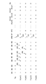
図3は、1つのフレームにおける複数の画素電極の極性を表す模式図である。図3中、データ線Xは、上述の各マルチプレクサ単位回路M1〜Msにより3本ずつ制御される。例えば、データ線X1、X2、X3は、図2のマルチプレクサ単位回路M1で制御される。
図3中、「+」、「−」の記号は、走査線Yとデータ線Xの交差に対応した画素電極の極性を示す。具体的には、「+」の記号は、画素電極が正極性であることを示す。「−」の記号は、画素電極が負極性であることを示す。
FIG. 3 is a schematic diagram showing the polarities of a plurality of pixel electrodes in one frame. In FIG. 3, three data lines X are controlled by each of the above-described multiplexer unit circuits M1 to Ms. For example, the data lines X1, X2, and X3 are controlled by the multiplexer unit circuit M1 in FIG.
In FIG. 3, the symbols “+” and “−” indicate the polarity of the pixel electrode corresponding to the intersection of the scanning line Y and the data line X. Specifically, the symbol “+” indicates that the pixel electrode is positive. The symbol “−” indicates that the pixel electrode has a negative polarity.
図3では、マルチプレクサ単位回路内において、複数の画素電極のうち走査線Y及びデータ線Xが延びる方向に隣接する2以上のものが同じ極性となっている。
例えば、走査線Y(a+1)に係る画素電極に注目すると、データ線X3、X4、X5との交差に対応する画素電極41A、41B、41Cは、正極性であり、X6、X7、X8との交差に対応する画素電極41D、41E、41Fは、負極性である。したがって、マルチプレクサ単位回路M2において、走査線Y(a+1)の延びる方向に隣接する3つの画素電極41B、41C、41Dのうち、画素電極41B、41Cの2つが同じ極性である。
また、例えば、データ線X10に係る画素電極に注目すると、走査線Ya、Y(a+1)との交差に対応する画素電極41G、41Hは、正極性であり、走査線Y(a+2)、Y(a+3)との交差に対応する画素電極41I、41Jは、負極性である。したがって、マルチプレクサ単位回路M4において、データ線X10の延びる方向に隣接する画素電極のうち、2つの画素電極41G、41H、及び、画素電極41I、41Jが、それぞれ、同じ極性である。
In FIG. 3, in the multiplexer unit circuit, two or more of the plurality of pixel electrodes adjacent in the direction in which the scanning line Y and the data line X extend have the same polarity.
For example, when attention is paid to the pixel electrode related to the scanning line Y (a + 1), the
For example, when attention is paid to the pixel electrode related to the data line X10, the
また、複数の画素電極のうち、異なるマルチプレクサ単位回路毎の境界で制御されるものが同じ極性となっている。
例えば、データ線X6、X7に係る画素電極に注目すると、走査線Y(a+1)との交差に対応する画素電極41D、41Eは、両方とも、負極性であり、走査線Y(a+2)との交差に対応する画素電極41K、41Lは、両方とも、正極性である。データ線X6、X7は、それぞれ、図2のマルチプレクサ単位回路M2、M3で制御されるので、異なるマルチプレクサ単位回路M1、M2で制御される画素電極41D、41E、及び、画素電極41K、41Lが、それぞれ、同じ極性である。
Among the plurality of pixel electrodes, those controlled at the boundaries of different multiplexer unit circuits have the same polarity.
For example, when attention is paid to the pixel electrodes related to the data lines X6 and X7, the
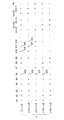
図4は、連続する複数のフレームにおける走査線Yaに係る画素電極の極性を表す模式図である。図4中、データ線Xは、上述の各マルチプレクサ単位回路M1〜Msにより3本ずつ制御される。例えば、データ線X1、X2、X3は、図2のマルチプレクサ単位回路M1で制御される。
図4中、「+」、「−」の記号は、走査線Yとデータ線Xの交差に対応した画素電極の極性を示す。具体的には、「+」の記号は、画素電極が正極性であることを示す。「−」の記号は、画素電極が負極性であることを示す。
FIG. 4 is a schematic diagram illustrating the polarity of the pixel electrode related to the scanning line Ya in a plurality of consecutive frames. In FIG. 4, three data lines X are controlled by each of the multiplexer unit circuits M1 to Ms described above. For example, the data lines X1, X2, and X3 are controlled by the multiplexer unit circuit M1 in FIG.
In FIG. 4, the symbols “+” and “−” indicate the polarity of the pixel electrode corresponding to the intersection of the scanning line Y and the data line X. Specifically, the symbol “+” indicates that the pixel electrode is positive. The symbol “−” indicates that the pixel electrode has a negative polarity.
図4において、画素電極が、それぞれ、連続する少なくとも2つ以上のフレームにおいて同じ極性となっている。
例えば、走査線Yaとデータ線X6の交差に対応した画素電極に注目すると、Jフレーム目、J+1フレーム目における画素電極41M、41Nは、負極性であり、J+2フレーム目、J+3フレーム目における画素電極41P、41Qは、正極性である。ここで、Jは自然数である。上述の画素電極41M、41N、41P、41Qは、フレームが異なるが、同一の画素電極であるので、画素電極が連続する2つのフレームにおいて同じ極性である。
In FIG. 4, each pixel electrode has the same polarity in at least two consecutive frames.
For example, when attention is paid to the pixel electrode corresponding to the intersection of the scanning line Ya and the data line X6, the
また、フレーム単位で複数の画素電極のうち極性が異なるもの同士の境界が変わっている。
例えば、Jフレーム目における走査線Yaに係る画素電極に注目すると、データ線X10、X11との交差に対応する画素電極41R、41Sは、それぞれ、正極性及び負極性である。つまり、Jフレーム目においては、極性が異なる画素電極同士の境界が、画素電極41R、41Sの間にある。
一方、J+1フレーム目における走査線Yaに係る画素電極に注目すると、データ線X11、X12との交差に対応する画素電極41T、41Uは、それぞれ、正極性及び負極性である。つまり、J+1フレーム目においては、極性が異なる画素電極同士の境界が、画素電極41T、41Uの間にある。
したがって、Jフレーム目からJ+1フレーム目に変わることで、極性が異なる画素電極同士の境界が変わっている。
In addition, the boundaries of the pixel electrodes having different polarities are changed in units of frames.
For example, when attention is paid to the pixel electrode related to the scanning line Ya in the J-th frame, the
On the other hand, paying attention to the pixel electrode related to the scanning line Ya in the J + 1 frame, the
Therefore, the boundary between pixel electrodes having different polarities is changed by changing from the J frame to the J + 1 frame.
本実施形態によれば、以下のような効果がある。
(1)マルチプレクサ単位回路内において、複数の画素電極のうち走査線Y及びデータ線Xが延びる方向に隣接する2以上のものが同じ極性となる。これにより、画素電極に交流電圧の画像信号を書き込めるため、電気光学物質が焼付くことを防止できる。また、極性の反転する回数を削減できるため、消費電力の増大を抑制できる。また、画素電極間で極性が異なるもの同士の境界の数を削減できるため、画素間のディスクリネーションの影響を抑制でき、コントラストの低下を抑制できる。さらに、1フレーム内に正極性の画素電極及び負極性の画素電極を混在させることで、フリッカを相殺させ、フリッカを抑制できる。
According to this embodiment, there are the following effects.
(1) In the multiplexer unit circuit, two or more adjacent ones of the plurality of pixel electrodes in the direction in which the scanning line Y and the data line X extend have the same polarity. Thereby, since an image signal of an alternating voltage can be written to the pixel electrode, it is possible to prevent the electro-optical material from being burned. In addition, since the number of times of polarity inversion can be reduced, an increase in power consumption can be suppressed. In addition, since the number of boundaries between the pixel electrodes having different polarities can be reduced, the influence of disclination between pixels can be suppressed, and a decrease in contrast can be suppressed. Furthermore, by mixing a positive pixel electrode and a negative pixel electrode in one frame, flicker can be offset and flicker can be suppressed.
(2)複数の画素電極のうち、異なるマルチプレクサ単位回路毎の境界で制御されるものが同じ極性となる。これにより、複数の画素電極のうち走査線Yが延びる方向に隣接し、かつ、異なるマルチプレクサ単位回路で制御されるもの同士において、極性が異なるもの同士の境界を無くすことができるため、上述の画素電極同士の間におけるディスクリネーションの影響を抑制でき、コントラストの低下を抑制できる。 (2) Among the plurality of pixel electrodes, those controlled at the boundaries of different multiplexer unit circuits have the same polarity. As a result, it is possible to eliminate the boundary between the pixel electrodes that are adjacent to each other in the direction in which the scanning line Y extends and are controlled by different multiplexer unit circuits and that have different polarities. The influence of disclination between the electrodes can be suppressed, and a decrease in contrast can be suppressed.
(3)複数の画素電極が、それぞれ、連続する少なくとも2つ以上のフレームにおいて同じ極性となる。これにより、極性の反転する回数を削減できるため、より消費電力の増大を抑制できる。 (3) Each of the plurality of pixel electrodes has the same polarity in at least two consecutive frames. Thereby, since the frequency | count of polarity inversion can be reduced, the increase in power consumption can be suppressed more.
(4)フレーム単位で画素電極のうち極性が異なるもの同士の境界が変わる。これにより、連続するフレームにおいて、複数の画素電極のうち極性が異なるもの同士の境界が同一の画素電極間で固定されるのを防止して、ブロックむらや電気光学物質の焼付きを防止できる。 (4) The boundaries between pixel electrodes having different polarities change in units of frames. Thereby, in a continuous frame, it can prevent that the boundary of what has a different polarity among several pixel electrodes is fixed between the same pixel electrodes, and can prevent block nonuniformity and the electro-optical substance from burning.
<2.第2実施形態>
図5は、本発明の第2実施形態に係るデータ線駆動回路30Aのブロック図である。データ線駆動回路30Aは、マルチプレクサの構成が、図2のデータ線駆動回路30と異なる。
<2. Second Embodiment>
FIG. 5 is a block diagram of a data
マルチプレクサ31Aは、データ線Xを6本ずつまとめて制御するマルチプレクサ単位回路N1〜Ntを含んで構成される。ここで、tは、2以上の自然数である。具体的には、マルチプレクサ単位回路N1〜Ntは、第1実施形態のマルチプレクサ単位回路M1〜Msを2つずつ一体化したものである。
The
図6は、1つのフレームにおける複数の画素電極の極性を表す模式図である。図6中、データ線Xは、上述の各マルチプレクサ単位回路N1〜Ntにより6本ずつ制御される点が、図3と異なる。 FIG. 6 is a schematic diagram showing the polarities of a plurality of pixel electrodes in one frame. 6 differs from FIG. 3 in that six data lines X are controlled by each of the multiplexer unit circuits N1 to Nt described above.
図7は、連続する複数のフレームにおける複数の画素電極の極性を表す模式図である。図7中、データ線Xは、上述の各マルチプレクサ単位回路N1〜Ntにより6本ずつ制御される点が、図4と異なる。 FIG. 7 is a schematic diagram showing the polarities of a plurality of pixel electrodes in a plurality of consecutive frames. 7 differs from FIG. 4 in that six data lines X are controlled by each of the above-described multiplexer unit circuits N1 to Nt.
本実施形態によれば、上述の(1)〜(4)に加え、以下のような効果がある。
(5)第1実施形態に係るデータ線駆動回路30では、データ線Xを3本ずつまとめて制御するマルチプレクサ単位回路M1〜Msを含んで構成されるのに対し、本実施形態に係るデータ線駆動回路30Aでは、データ線Xを6本ずつまとめて制御するマルチプレクサ単位回路N1〜Ntを含んで構成される。このため、同数のデータ線Xを制御する場合、データ線駆動回路30と比べて、データ線駆動回路30Aの方が、マルチプレクサ単位回路が少なくなる。
According to the present embodiment, in addition to the above (1) to (4), there are the following effects.
(5) The data line driving
<3.変形例>
なお、本発明は上述の実施形態に限定されるものではなく、本発明の目的を達成できる範囲での変形、改良等は本発明に含まれるものである。
例えば、複数の画素電極のうち走査線が延びる方向に隣接する3つのものを、またデータ線が延びる方向に隣接する2つのものを、それぞれ同じ極性としたが、これに限らず、5つのものが同じ極性であってもよい。
<3. Modification>
In addition, this invention is not limited to the above-mentioned embodiment, The deformation | transformation in the range which can achieve the objective of this invention, improvement, etc. are included in this invention.
For example, three of the plurality of pixel electrodes adjacent to each other in the direction in which the scanning line extends and two adjacent to each other in the direction in which the data line extends have the same polarity. May be of the same polarity.
また、上述の各実施形態では、本発明を液晶を用いた電気光学装置1に適用したが、これに限らず、液晶以外の電気光学物質を用いた電気光学装置にも適用できる。電気光学物質とは、電気信号(電流信号または電圧信号)の供給によって透過率や輝度といった光学的特性が変化する物質である。例えば、有機EL(Electro Luminescent)や発光ポリマーなどのOLED素子を電気光学物質として用いた表示パネルや、着色された液体とこの液体に分散された白色の粒子とを含むマイクロカプセルを電気光学物質として用いた電気泳動表示パネル、極性が相違する領域ごとに異なる色に塗り分けられたツイストボールを電気光学物質として用いたツイストボールディスプレイパネル、黒色トナーを電気光学物質として用いたトナーディスプレイパネル、あるいは、ヘリウムやネオン等の高圧ガスを電気光学物質として用いたプラズマディスプレイパネルなど各種の電気光学装置に対しても、上記実施形態と同様に本発明が適用され得る。
In each of the above-described embodiments, the present invention is applied to the electro-
<4.電気光学装置>
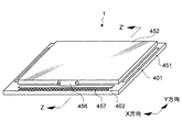
図8は、上述の実施形態及び変形例に係る電気光学装置1の構成を示す斜視図であり、図9は、図8におけるZ−Z´断面図である。
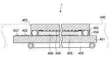
電気光学装置1は、筐体400(図9中破線で示す)に収納されている。電気光学装置1は、画素電極406等が形成された素子基板451と、この素子基板451に対向配置されかつ共通電極42等が形成された対向基板452と、素子基板451及び対向基板452の間に設けられた電気光学物質としての液晶455と、素子基板451の下側(対向基板452とは反対側)に設けられて液晶455に光を照射する光源としてのバックライト450と、を有する。素子基板451は、ガラスや半導体等で形成され、この素子基板451上には、TFT(Thin Film Transistor:薄膜トランジスタ)を用いて各種の回路等が形成される。また、対向基板452は、ガラス等の透明性の材料で形成される。
<4. Electro-optical device>
FIG. 8 is a perspective view illustrating the configuration of the electro-
The electro-
対向基板452の外周部には、素子基板451及び対向基板452の間隙を封止するシール部材454が設けられている。このシール部材454は、素子基板451及び対向基板452とともに、液晶455が封入される空間を形成する。シール部材454には、素子基板451及び対向基板452の間隔を保持するため、スペーサ453が混入されている。なお、シール部材454には、液晶455を封入するための開口部が形成されており、この開口部は、液晶455の封入後に封止材456で封止されている。
A
ここで、素子基板451の対向基板452側の表面であって、シール部材454の一辺の外側には、Y方向に延在するデータ線を駆動するデータ線駆動回路401が形成されている。さらに、この一辺には複数の接続電極457が形成されて、この接続電極457を通して各種信号が入力される。また、シール部材454の前記一辺の両側の辺には、X方向に延在する後述する走査線を駆動する走査線駆動回路402が形成されている。
Here, a data
<5.電子機器>
次に、上述した実施形態に係る電気光学装置1を適用した電子機器について説明する。図10に、電気光学装置1を適用した携帯電話機の構成を示す。携帯電話機3000は、複数の操作ボタン3001及びスクロールボタン3002、ならびに表示ユニットとしての電気光学装置1を有する。スクロールボタン3002を操作することによって、電気光学装置1に表示される画面がスクロールされる。
<5. Electronic equipment>
Next, an electronic apparatus to which the electro-
1…電気光学装置、10…画素マトリクス、20…走査線駆動回路、30、30A…データ線駆動回路、31、31A…マルチプレクサ、41…画素電極、42…共通電極、43…TFT、X…データ線、Y…走査線。
DESCRIPTION OF
Claims (3)
前記画素に設けられ、スイッチング素子を介して前記データ線に接続される画素電極と、
前記画素電極と対向する共通電極と、
当該共通電極の電位を基準として高電位側の正極性画像信号及び低電位側の負極性画像信号を、前記データ線に供給するデータ線駆動回路を有し、
前記データ線駆動回路は、
前記データ線のうち隣り合う3本以上のデータ線をまとめて制御するマルチプレクサ単位回路を備え、
前記マルチプレクサ単位回路を介して、
前記隣り合う3本以上のデータ線のうちの一部に対して前記正極性画像信号と前記負極性画像信号とのいずれか一方を供給し、
前記隣り合う3本以上のデータ線のうちの残りに対して前記正極性画像信号と前記負極性画像信号とのいずれか他方を供給し、
前記隣り合う3本以上のデータ線のうちの他のマルチプレクサ単位回路に制御されるデータ線に隣り合うデータ線と前記隣り合うデータ線に隣り合う前記他のマルチプレクサ単位回路に制御されるデータ線とに対して、フレームが変わっても、同じ極性の前記正極性画像信号または前記負極性画像信号を供給し、
前記正極性画像信号が供給されるデータ線と前記負極性画像信号が供給されるデータ線とが隣り合う境界が、フレーム単位で変わるように、前記正極性画像信号及び前記負極性画像信号を供給する、
ことを特徴とする電気光学装置。 In an electro-optical device having a pixel provided corresponding to the intersection of a scanning line and a data line,
A pixel electrode provided in the pixel and connected to the data line via a switching element;
A common electrode facing the pixel electrode;
A data line driving circuit for supplying a high-potential-side positive image signal and a low-potential-side negative image signal to the data line with reference to the potential of the common electrode;
The data line driving circuit includes:
A multiplexer unit circuit that collectively controls three or more adjacent data lines of the data lines;
Through the multiplexer unit circuit,
Supplying either one of the positive image signal and the negative image signal to a part of the three or more adjacent data lines;
Supplying the other of the positive polarity image signal and the negative polarity image signal to the rest of the three or more adjacent data lines;
A data line controlled in addition to the other multiplexer unit circuit adjacent to the data line adjacent the data line adjacent to the data line controlled in multiplexer unit circuit among the three or more data lines, wherein the adjacent In contrast , even if the frame changes, the positive polarity image signal or the negative polarity image signal having the same polarity is supplied ,
The positive image signal and the negative image signal are supplied so that the boundary between the data line to which the positive image signal is supplied and the data line to which the negative image signal is supplied changes in units of frames. To
An electro-optical device.
前記画素に設けられた画素電極と前記データ線とを、前記走査線からの制御信号に応じてスイッチング素子を介して接続し、
前記画素電極と対向して形成された共通電極の電位を基準として高電位側の正極性画像信号及び低電位側の負極性画像信号を、前記データ線のうち隣り合う3本以上のデータ線をまとめて制御するマルチプレクサ単位回路を介して前記データ線に供給し、
前記マルチプレクサ単位回路により制御される前記隣り合う3本以上のデータ線のうちの一部に対して前記正極性画像信号と前記負極性画像信号とのいずれか一方を供給し、
前記マルチプレクサ単位回路により制御される前記隣り合う3本以上のデータ線のうちの残りに対して前記正極性画像信号と前記負極性画像信号とのいずれか他方を供給し、
前記隣り合う3本以上のデータ線のうちの他のマルチプレクサ単位回路に制御されるデータ線と隣り合うデータ線に、前記隣り合うデータ線と隣り合う前記他のマルチプレクサ単位回路に制御されるデータ線とに対して、フレームが変わっても、同じ極性の前記正極性画像信号または前記負極性画像信号を供給し、
前記正極性画像信号が供給されるデータ線と前記負極性画像信号が供給されるデータ線とが隣り合う境界が、フレーム単位で変わるように、前記正極性画像信号及び前記負極性画像信号を供給する
ことを特徴とする電気光学装置の駆動方法。 In a driving method of an electro-optical device having pixels provided corresponding to intersections of a plurality of scanning lines and a plurality of data lines,
The pixel electrode provided in the pixel and the data line are connected via a switching element according to a control signal from the scanning line,
The positive image signal on the high potential side and the negative image signal on the low potential side with respect to the potential of the common electrode formed facing the pixel electrode, and three or more adjacent data lines among the data lines Supply to the data line through a multiplexer unit circuit that collectively control,
Supplying one of the positive image signal and the negative image signal to a part of the three or more adjacent data lines controlled by the multiplexer unit circuit;
Supplying the other of the positive-polarity image signal and the negative-polarity image signal to the remainder of the three or more adjacent data lines controlled by the multiplexer unit circuit;
A data line adjacent to the data line controlled by the other multiplexer unit circuit among the three or more data lines, wherein adjacent data lines controlled by the other multiplexer unit circuit adjacent to the data lines where the adjacent In contrast , even if the frame changes, the positive polarity image signal or the negative polarity image signal having the same polarity is supplied ,
The positive image signal and the negative image signal are supplied so that the boundary between the data line to which the positive image signal is supplied and the data line to which the negative image signal is supplied changes in units of frames. A method for driving an electro-optical device.
Priority Applications (1)
| Application Number | Priority Date | Filing Date | Title |
|---|---|---|---|
| JP2005156682A JP5162811B2 (en) | 2005-05-30 | 2005-05-30 | Electro-optical device, driving method of electro-optical device, and electronic apparatus |
Applications Claiming Priority (1)
| Application Number | Priority Date | Filing Date | Title |
|---|---|---|---|
| JP2005156682A JP5162811B2 (en) | 2005-05-30 | 2005-05-30 | Electro-optical device, driving method of electro-optical device, and electronic apparatus |
Related Child Applications (1)
| Application Number | Title | Priority Date | Filing Date |
|---|---|---|---|
| JP2012023875A Division JP2012123411A (en) | 2012-02-07 | 2012-02-07 | Electro-optic device and electronic apparatus |
Publications (2)
| Publication Number | Publication Date |
|---|---|
| JP2006330537A JP2006330537A (en) | 2006-12-07 |
| JP5162811B2 true JP5162811B2 (en) | 2013-03-13 |
Family
ID=37552261
Family Applications (1)
| Application Number | Title | Priority Date | Filing Date |
|---|---|---|---|
| JP2005156682A Expired - Fee Related JP5162811B2 (en) | 2005-05-30 | 2005-05-30 | Electro-optical device, driving method of electro-optical device, and electronic apparatus |
Country Status (1)
| Country | Link |
|---|---|
| JP (1) | JP5162811B2 (en) |
Families Citing this family (1)
| Publication number | Priority date | Publication date | Assignee | Title |
|---|---|---|---|---|
| CN107993629B (en) * | 2018-01-31 | 2020-05-29 | 武汉华星光电技术有限公司 | Driving method of liquid crystal display device |
Family Cites Families (5)
| Publication number | Priority date | Publication date | Assignee | Title |
|---|---|---|---|---|
| JPS6368821A (en) * | 1986-09-11 | 1988-03-28 | Fujitsu Ltd | Driving method for active matrix type liquid crystal panel |
| JP4683679B2 (en) * | 1998-03-27 | 2011-05-18 | 株式会社半導体エネルギー研究所 | Driving method of liquid crystal display device |
| JP3956748B2 (en) * | 2001-06-26 | 2007-08-08 | セイコーエプソン株式会社 | Display device, driving circuit thereof, driving method thereof, and electronic apparatus |
| JP2004219823A (en) * | 2003-01-16 | 2004-08-05 | Toshiba Matsushita Display Technology Co Ltd | Liquid crystal display device |
| JP4434628B2 (en) * | 2003-05-29 | 2010-03-17 | 三菱電機株式会社 | Liquid crystal display |
-
2005
- 2005-05-30 JP JP2005156682A patent/JP5162811B2/en not_active Expired - Fee Related
Also Published As
| Publication number | Publication date |
|---|---|
| JP2006330537A (en) | 2006-12-07 |
Similar Documents
| Publication | Publication Date | Title |
|---|---|---|
| JP5414974B2 (en) | Liquid crystal display | |
| US7116297B2 (en) | Liquid crystal display device and driving method for liquid crystal display device | |
| KR101072375B1 (en) | Liquid Crystal Display Device Automatically Adjusting Aperture Ratio In Each Pixel | |
| KR100683459B1 (en) | Electro-optical device, method of driving electro-optical device, and electronic apparatus | |
| JP4331192B2 (en) | Liquid crystal display device and driving method thereof | |
| JP2008076416A (en) | Driving device for display panel, display panel, display device with the same, and driving method for display panel | |
| US8384656B2 (en) | Driving device, electro-optical device, and electronic apparatus | |
| KR101322031B1 (en) | Flat panel display controllable viewing angle and multi-view | |
| JP2007108615A (en) | Electro-optical device, method of driving electro-optical device, and electronic equipment | |
| KR101082286B1 (en) | Liquid Crystal Display Device and Driving Method Thereof | |
| KR100759697B1 (en) | Liquid crystal display device and driving method thereof | |
| KR20020052137A (en) | Liquid crystal display | |
| JP2013195869A (en) | Liquid crystal display apparatus, method of driving liquid crystal display apparatus, and electronic apparatus | |
| KR101074381B1 (en) | A in-plain switching liquid crystal display device | |
| TWI416497B (en) | Driving method for liquid crystal display device and related device | |
| US20040239605A1 (en) | Device and method for driving polarity inversion of electrodes of LCD panel | |
| JP5162811B2 (en) | Electro-optical device, driving method of electro-optical device, and electronic apparatus | |
| KR101113997B1 (en) | Liquid crystal display and method for driving the same | |
| KR100499578B1 (en) | driving circuit of liquid crystal display device | |
| US7812911B2 (en) | Liquid crystal display | |
| JP2012123411A (en) | Electro-optic device and electronic apparatus | |
| JP2006171084A (en) | Liquid crystal display apparatus and drive method for the same | |
| US11694647B2 (en) | Display device | |
| JP2005107527A (en) | Liquid crystal display device of field sequential driving system | |
| US20160063930A1 (en) | Electro-optical device and electronic apparatus |
Legal Events
| Date | Code | Title | Description |
|---|---|---|---|
| RD04 | Notification of resignation of power of attorney |
Free format text: JAPANESE INTERMEDIATE CODE: A7424 Effective date: 20070403 |
|
| A621 | Written request for application examination |
Free format text: JAPANESE INTERMEDIATE CODE: A621 Effective date: 20070710 |
|
| A977 | Report on retrieval |
Free format text: JAPANESE INTERMEDIATE CODE: A971007 Effective date: 20100611 |
|
| A131 | Notification of reasons for refusal |
Free format text: JAPANESE INTERMEDIATE CODE: A131 Effective date: 20101214 |
|
| A521 | Written amendment |
Free format text: JAPANESE INTERMEDIATE CODE: A523 Effective date: 20110210 |
|
| A02 | Decision of refusal |
Free format text: JAPANESE INTERMEDIATE CODE: A02 Effective date: 20111108 |
|
| A521 | Written amendment |
Free format text: JAPANESE INTERMEDIATE CODE: A523 Effective date: 20120207 |
|
| A911 | Transfer of reconsideration by examiner before appeal (zenchi) |
Free format text: JAPANESE INTERMEDIATE CODE: A911 Effective date: 20120214 |
|
| A131 | Notification of reasons for refusal |
Free format text: JAPANESE INTERMEDIATE CODE: A131 Effective date: 20120918 |
|
| A521 | Written amendment |
Free format text: JAPANESE INTERMEDIATE CODE: A523 Effective date: 20121030 |
|
| TRDD | Decision of grant or rejection written | ||
| A01 | Written decision to grant a patent or to grant a registration (utility model) |
Free format text: JAPANESE INTERMEDIATE CODE: A01 Effective date: 20121120 |
|
| A61 | First payment of annual fees (during grant procedure) |
Free format text: JAPANESE INTERMEDIATE CODE: A61 Effective date: 20121203 |
|
| FPAY | Renewal fee payment (event date is renewal date of database) |
Free format text: PAYMENT UNTIL: 20151228 Year of fee payment: 3 |
|
| R150 | Certificate of patent or registration of utility model |
Ref document number: 5162811 Country of ref document: JP Free format text: JAPANESE INTERMEDIATE CODE: R150 Free format text: JAPANESE INTERMEDIATE CODE: R150 |
|
| R250 | Receipt of annual fees |
Free format text: JAPANESE INTERMEDIATE CODE: R250 |
|
| LAPS | Cancellation because of no payment of annual fees |