JP3956242B2 - Offset removal and spatial frequency band filtering circuit and method for light receiving device signal - Google Patents
Offset removal and spatial frequency band filtering circuit and method for light receiving device signal Download PDFInfo
- Publication number
- JP3956242B2 JP3956242B2 JP00082897A JP82897A JP3956242B2 JP 3956242 B2 JP3956242 B2 JP 3956242B2 JP 00082897 A JP00082897 A JP 00082897A JP 82897 A JP82897 A JP 82897A JP 3956242 B2 JP3956242 B2 JP 3956242B2
- Authority
- JP
- Japan
- Prior art keywords
- circuit
- output
- amplifier
- signal
- input
- Prior art date
- Legal status (The legal status is an assumption and is not a legal conclusion. Google has not performed a legal analysis and makes no representation as to the accuracy of the status listed.)
- Expired - Lifetime
Links
Images


Classifications
-
- H—ELECTRICITY
- H03—ELECTRONIC CIRCUITRY
- H03F—AMPLIFIERS
- H03F3/00—Amplifiers with only discharge tubes or only semiconductor devices as amplifying elements
- H03F3/45—Differential amplifiers
- H03F3/45071—Differential amplifiers with semiconductor devices only
- H03F3/45076—Differential amplifiers with semiconductor devices only characterised by the way of implementation of the active amplifying circuit in the differential amplifier
- H03F3/45475—Differential amplifiers with semiconductor devices only characterised by the way of implementation of the active amplifying circuit in the differential amplifier using IC blocks as the active amplifying circuit
-
- H—ELECTRICITY
- H03—ELECTRONIC CIRCUITRY
- H03F—AMPLIFIERS
- H03F1/00—Details of amplifiers with only discharge tubes, only semiconductor devices or only unspecified devices as amplifying elements
- H03F1/30—Modifications of amplifiers to reduce influence of variations of temperature or supply voltage or other physical parameters
- H03F1/303—Modifications of amplifiers to reduce influence of variations of temperature or supply voltage or other physical parameters using a switching device
-
- H—ELECTRICITY
- H03—ELECTRONIC CIRCUITRY
- H03F—AMPLIFIERS
- H03F3/00—Amplifiers with only discharge tubes or only semiconductor devices as amplifying elements
- H03F3/04—Amplifiers with only discharge tubes or only semiconductor devices as amplifying elements with semiconductor devices only
- H03F3/08—Amplifiers with only discharge tubes or only semiconductor devices as amplifying elements with semiconductor devices only controlled by light
- H03F3/087—Amplifiers with only discharge tubes or only semiconductor devices as amplifying elements with semiconductor devices only controlled by light with IC amplifier blocks
-
- H—ELECTRICITY
- H04—ELECTRIC COMMUNICATION TECHNIQUE
- H04N—PICTORIAL COMMUNICATION, e.g. TELEVISION
- H04N25/00—Circuitry of solid-state image sensors [SSIS]; Control thereof
- H04N25/60—Noise processing, e.g. detecting, correcting, reducing or removing noise
- H04N25/67—Noise processing, e.g. detecting, correcting, reducing or removing noise applied to fixed-pattern noise, e.g. non-uniformity of response
- H04N25/671—Noise processing, e.g. detecting, correcting, reducing or removing noise applied to fixed-pattern noise, e.g. non-uniformity of response for non-uniformity detection or correction
- H04N25/677—Noise processing, e.g. detecting, correcting, reducing or removing noise applied to fixed-pattern noise, e.g. non-uniformity of response for non-uniformity detection or correction for reducing the column or line fixed pattern noise
-
- H—ELECTRICITY
- H04—ELECTRIC COMMUNICATION TECHNIQUE
- H04N—PICTORIAL COMMUNICATION, e.g. TELEVISION
- H04N25/00—Circuitry of solid-state image sensors [SSIS]; Control thereof
- H04N25/70—SSIS architectures; Circuits associated therewith
- H04N25/701—Line sensors
-
- H—ELECTRICITY
- H04—ELECTRIC COMMUNICATION TECHNIQUE
- H04N—PICTORIAL COMMUNICATION, e.g. TELEVISION
- H04N25/00—Circuitry of solid-state image sensors [SSIS]; Control thereof
- H04N25/70—SSIS architectures; Circuits associated therewith
- H04N25/71—Charge-coupled device [CCD] sensors; Charge-transfer registers specially adapted for CCD sensors
- H04N25/75—Circuitry for providing, modifying or processing image signals from the pixel array
-
- H—ELECTRICITY
- H04—ELECTRIC COMMUNICATION TECHNIQUE
- H04N—PICTORIAL COMMUNICATION, e.g. TELEVISION
- H04N25/00—Circuitry of solid-state image sensors [SSIS]; Control thereof
- H04N25/70—SSIS architectures; Circuits associated therewith
- H04N25/76—Addressed sensors, e.g. MOS or CMOS sensors
- H04N25/767—Horizontal readout lines, multiplexers or registers
-
- H—ELECTRICITY
- H04—ELECTRIC COMMUNICATION TECHNIQUE
- H04N—PICTORIAL COMMUNICATION, e.g. TELEVISION
- H04N25/00—Circuitry of solid-state image sensors [SSIS]; Control thereof
- H04N25/70—SSIS architectures; Circuits associated therewith
- H04N25/76—Addressed sensors, e.g. MOS or CMOS sensors
- H04N25/77—Pixel circuitry, e.g. memories, A/D converters, pixel amplifiers, shared circuits or shared components
-
- H—ELECTRICITY
- H03—ELECTRONIC CIRCUITRY
- H03F—AMPLIFIERS
- H03F2200/00—Indexing scheme relating to amplifiers
- H03F2200/249—A switch coupled in the input circuit of an amplifier being controlled by a circuit, e.g. feedback circuitry being controlling the switch
-
- H—ELECTRICITY
- H03—ELECTRONIC CIRCUITRY
- H03F—AMPLIFIERS
- H03F2203/00—Indexing scheme relating to amplifiers with only discharge tubes or only semiconductor devices as amplifying elements covered by H03F3/00
- H03F2203/45—Indexing scheme relating to differential amplifiers
- H03F2203/45212—Indexing scheme relating to differential amplifiers the differential amplifier being designed to have a reduced offset
Landscapes
- Engineering & Computer Science (AREA)
- Multimedia (AREA)
- Signal Processing (AREA)
- Power Engineering (AREA)
- Transforming Light Signals Into Electric Signals (AREA)
- Facsimile Scanning Arrangements (AREA)
- Facsimile Heads (AREA)
- Light Receiving Elements (AREA)
- Amplifiers (AREA)
Description
【0001】
【発明の属する技術分野】
本発明は、一般に、信号転送回路に関し、とりわけ、受光装置アレイからの個々の信号を計算回路に転送するための回路構成に関する。
【0002】
【従来の技術】
さまざまな用途において、ある表面を横切る装置経路を正確に判定することが重要である。例えば、走査原稿の画像の忠実な再現を獲得すべき場合、原稿に沿った走査装置の走行に関する正確な情報がなければならない。一般に、スキャナによって得られる捕捉画像は、デジタル・フォーマットでメモリに記憶される画素データ列である。歪みのない画像には、画素データ列への原稿画像の忠実なマッピングが必要とされる。
【0003】
本発明の譲受人に譲渡された、Ertel 他に対する米国特許第5,149,980 号に記載されているところでは、相互相関関数を用いて、所定の方向への原稿と光電素子アレイとの間の相対移動が判定される。該特許に言及されているところによれば、1次元手法を拡張して、原稿と光電素子アレイとの間の2次元相対移動を判定し、それにより、2次元平面における並進、回転、及び変倍が追跡可能となる。
【0004】
Ertel 他に対する特許に記載されているところによれば、光センサ・アレイを用いて、原稿のある形態の「識別特性」が収集される。この識別特性は、原稿の表面質感または他の光学特徴を照射して、画像形成することによって得ることができる。光強度は、表面質感の変化に伴いピクセル毎に変動する。原稿の表面の相互相関画像によって、アレイと原稿との間の相対移動を突き止めることが可能である。
【0005】
【発明が解決しようとする課題】
Ertel 他によって解説されているようなシステムの設計に関する厳密な要素は、原稿の識別特性を確実に判定するのに十分な高レベルに、各光電素子のS/N比を維持する回路である。信号が、白紙の紙質のわずかな変化の結果として、画素から画素への反射率の差である場合、反射率の変化は、約6パーセントになる可能性がある。サンプル速度目標、及び可能性のある後続の信号平均化量を考慮すると、有効な情報を得ようとすれば、信号におけるノイズ条件は、紙反射率変動信号の6パーセント未満でなければならない。
【0006】
従って、ノイズは、受光装置アレイにおける光電素子からの信号に処理を加える上での問題の1つである。別の問題は、製造段階で導入される、処理回路の性能のばらつきである。電気的に並列な転送回路の性能がばらつくと、ある画素から他の画素への反射率の差の計算に頼る動作は、エラーを被りやすい。理想的には、信号転送回路の性能のばらつきに起因した画素間の信号差がなく、そのため、画素信号間の差が、光電素子における受光の差だけに帰属する。しかし、回路デバイスには、そのデバイスが、同じ製造プロセスによって形成された場合であっても、性能にばらつきがある。
【0007】
更に他の問題には、画素の1つ近傍における画素間では一貫しているが、画素近傍同志の間では異なるような、画像に影響を及ぼす考慮事項が存在する場合に、画像形成される表面に関する有効な情報を確実に得ることが含まれる。例えば、照射光学装置によって、画像形成すべき表面の、近傍間における照度変動を一貫させることができる。不均一な照度は、人為物を生じさせることになる。一貫した局所的パターンの他の例として、光電素子アレイの一部が、暗い背景を有する表面領域に向けられており、一方、光電素子の残りの部分は、表面の陰影のない領域に向けられているパターンがある。
【0008】
従って、本発明の目的は、製造段階で導入されるデバイスのばらつきにより、また光電素子信号の多数画素パターン発生及び/又は処理により生じるエラーに対する感受性を低減した、受光装置配列に接続するための転送回路を提供することである。
【0009】
【課題を解決するための手段】
上記目的は、本発明の1つの実施例の場合、周期的オフセット補正を受けて、転送増幅器間における性能の差に対して信号処理の感受性を低減する、並列転送増幅器を含む、光電素子アレイから計算回路に信号を転送するための回路及び方法により達成される。
【0010】
上記目的は、本発明の他の実施例の場合、光電素子アレイにおける光受信の多数光電素子パターンのような人為物の影響を抑制する空間周波数帯域フィルタリング増幅器を含む、信号転送回路によって達成される。
【0011】
以下の開示において、「DC除去」という用語は、空間周波数帯域フィルタリングを表すための簡略用語として用いられる。ここで理解されたいのは、本明細書で用いるような「DC除去」という用語には、DC空間成分の除去だけでなく、低周波数と高周波数の一方または両方における、空間周波数成分の除去も又包含される、ということである。
【0012】
転送増幅器レベルにおいて、読み出しモードの場合、各転送増幅器は第1の入力を有し、これは、光電素子で受けた光を表す信号を受信するように接続される。アレイ内の光電素子は、列と行をなすように配列され、特定の列における光電素子は、特定の転送増幅器の第1の入力に順次接続されるが、これは厳密ではない。各転送増幅器は、基準電圧源(例えば、1.75ボルト)に接続される第2の入力を有する。転送増幅器は、差動回路として機能するので、出力は、第1と第2の入力における電圧状態間の差に応答することになる。しかし、読み出し期間の間のリセット期間時には、第1と第2の入力は、両方とも、基準電圧源に接続される。さらに、転送増幅器の出力は、瞬間的にリセット電圧源(例えば、3.25ボルト)に接続される。オフセット低減回路が設けられて、出力がリセット電圧源から切断された後に、リセット電圧と出力での電圧状態との間の電圧差の検出に応答して、オフセット調整信号が発生される。このようにして、調整信号を問題となる転送増幅器に加えることによって、その転送増幅器と他の転送増幅器との間における性能差を低減、又は削除することが可能になる。
【0013】
オフセット調整型の転送増幅器の利点は、デバイス間のばらつき及び1/fノイズの影響が考慮されるという点にある。アレイ全体を読み出すためのサイクル時間は、50μs程度である。高回路密度と共に低電力動作を達成するためには、CMOS回路が望ましいが、仮に1/fノイズが抑制されないとすれば、こうしたノイズによって、増幅器の出力に大幅な揺らぎを生じる可能性がある。本発明の他の利点は、各転送増幅器には、オフセット調整信号を格納するサンプル/ホールド構成が含まれているため、各転送増幅器に必要なのは、周期的にリフレッシュされることだけとなる点にある。従って、オフセット調整信号を決める単一回路を全ての転送増幅器に用いることが可能になる。光電素子信号読み出し間における期間を延長することなく、周期的なリフレッシュを実現するタイミング・シーケンスが規定される。
【0014】
各転送増幅器には、サンプル/ホールド構成が含まれているので、転送増幅器は3つの動作モードを備えている。読み出しモードの場合、第2の入力が基準電圧源に接続され、一方、第1の入力が光電素子に接続される。結果として、電荷が、動作上関連する積分コンデンサに転送される。増幅器出力電圧は、次いで、下流の処理回路に供給される。内部のサンプル/ホールド構成によって、オフセット補正が施される。第2の動作モードは、受動リセット・モードである。オフセット調整信号が更新されないので、このリセットは「受動」である。第1の能動オフセット調整動作が実行されるまで、受動リセット・モードは低品質である。受動リセット・モードの場合、転送増幅器の2つの入力が互いに接続され、その出力は、リセット電圧源に接続されたままである。第3の動作モードは、能動リセット・モードである。受動リセット・モードのように、転送増幅器の2つの入力が基準電圧源に接続される。しかし、その出力は、瞬間的にリセット電圧源に接続されるだけである。出力は、切断されると、オフセット調整回路に接続され、適正なオフセット調整信号が決定されて、次の能動リセット動作まで、サンプル/ホールド構成によって記憶される。
【0015】
オフセット調整信号の周期的更新の間に、各転送増幅器は、交互に読み出しモードと受動リセット・モードになる。1/fオフセット・ドリフト成分は、十分に低速のため、光電素子アレイの各8番目の読み出し後の更新でも、十分な速度である。
【0016】
前記のように、本発明には、多数光電素子光パターン、及び他の人為物を抑制するDC除去増幅器も含まれている。DC除去増幅器によって、転送増幅器の出力から、低周波数と高周波数の両方の空間周波数成分が除去される。DC除去増幅器と転送増幅器は、1対1の対応とすることができる。各DC除去増幅器には、特定の光電素子から問題となる信号を受信するように接続された、一次入力が含まれている。各DC除去増幅器には、特定の光電素子に近接した光電素子から出力信号を受信するように接続された、少なくとも1つの二次入力も含まれている。要するに、二次入力の平均化が行われて、結果得られる平均値が一次入力から減算される。DC除去増幅器は、低空間周波数成分を除去する以外に、画素間隔の2倍に相当する周波数において固有の低域通過特性を備えている。従って、DC除去増幅器は、本質的に帯域通過特性を備えている。帯域通過特性の固有の低域通過要素は、平均化の前に、二次入力を異なる重み係数で乗算することによって修正することが可能である。重み係数は、正または負の数となり得る。
【0017】
DC除去増幅器は、第1と第2の差動セルから形成され、第2の差動セルは、その出力からその入力への負帰還ループを備えている。第2の差動セルは又、下流の差動動作を容易にする中間範囲の電圧を確立するために、DC入力も備える。本発明にとって不可欠ではないが、DC除去増幅器が、オフセット補正を含むこともでき、またスイッチング・ネットワークを含むこともでき、これによりユーザが、入力をDC除去増幅器に切り換えたり、又は増幅器の動作をテスト・モードに設定したりすることが可能となる。
【0018】
【発明の実施の形態】
図1を参照すると、原稿14に沿った曲がりくねった経路12を辿った、携帯用手持ち式走査装置10が示されている。原稿は、1枚の紙とすることもできるが、本発明は、他の画像を保持する基体に用いることもできる。手持ち式走査装置を利用する場合、紙の繊維といった固有の構造特徴の位置を追跡して、結果得られる位置情報を利用して、画像データを修正することができる。しかしながら、本発明は、他の用途でも利用することができる。
【0019】
走査装置10は、自立式で、バッテリで動作することが望ましい。しかし、該装置には、外部電源、あるいは、コンピュータ又はネットワークのデータ・ポートに対する接続部を含めることもできる。この走査装置には、画像ディスプレイ16が含まれている。該ディスプレイによって、捕捉した画像をほぼ瞬時に見ることが可能になる。ただしディスプレイは、不可欠ではない。
【0020】
走査装置10は、3つの自由度を可能にし、その2つは並進であり、1つは回転である。第1の自由度は、原稿14に沿った横への移動(X軸移動)である。第2の自由度は、原稿に沿った上下方向の移動(Y軸移動)である。第3の自由度は、原稿14のエッジに対して、画像センサ素子の線形アレイが回転不整合(Z軸移動の結果としてのθ不整合)となるように、該装置を動作させる能力である。すなわち、必ずしも画像形成素子の線形アレイを装置の並進方向と垂直に維持する必要はない。
【0021】
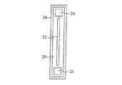
次に、図1及び2を参照すると、走査装置10の底側18には、原稿14と撮像センサ22の間の適切な接触を維持する際に手助けとなる、枢動部材20が含まれている。航行センサ24及び26が、撮像センサの対向端に配置されている。航行センサは枢動部材に装着されているので、航行センサは撮像センサに対して固定位置にある。
【0022】
物理的に小型化にするために、撮像センサ22は、接触式の画像形成装置が望ましいが、小型化がそれほど問題でない、又は更に小さい画像が所望される用途の場合、投射光学装置を用いたセンサを使用することもでき、これは倍率が1未満である。接触式の画像形成装置は、一般に、日本板硝子社の米国連邦登録商標であるSELFOCの商標名で販売されているレンズを使用する。あまり慣用的ではないが、結像レンズを用いずに、光源のインターリーブ型アレイ素子と近接センサを利用して、接触式の画像形成をなすことが可能である。走査用途のための慣用的な撮像センサを用いることもできる。撮像センサは、やはり照明光源、照明光学装置、及び像伝送光学装置を含む1つのユニットの一部とすることもできる。
【0023】
図1には、4つと何分の1かの帯状部分、すなわち原稿14を横切る側方パスからなる、曲がりくねった経路12が示されている。大部分の用途にとって有効な撮像センサ22は、25mm〜100mmの範囲内の長さを有する。帯状部分には、重複した領域が含まれるべきであり、その結果、ステッチ・プロセスを利用して、被走査原稿の忠実な再現を得ることができる。
【0024】
航行センサ
走査装置10には、少なくとも1つの航行センサ24又は26が含まれている。好適な実施例の場合、該装置には、1対の航行センサが含まれ、これらのセンサは、撮像センサ22の対向端に配置される。互いに直交して装着される光電素子の1次元アレイを利用することができるが、更に好適な実施例の場合、各航行センサは、光電素子の2次元アレイである。航行センサ24及び26を用いて、原稿に対する走査装置10の移動が追跡される。
【0025】
各航行センサは、読み出し及び信号処理回路を含む集積回路基板に形成される、光電素子のアレイである。40μmの画素距離の範囲にわたって必要な位置精度は、2.0μmである。非常に高い位置精度には、素子間で十分に異なる信号を獲得するために、長さ数十ミクロン以下の個別の光電素子が必要になる。好適な実施例の場合、紙の原稿14上で所望される画素サイズは、40μmであり、画像形成光学装置によって、1.5の倍率が得られるので、航行センサ24及び26の受光素子は、60μm×60μmになる。光学倍率が大きくなると、より大きい画素の利用が可能になる。しかし、必要とされるシリコンの総面積、従って、アレイのコストを最小限に抑えるためには、性能目標に合うように、画素サイズをできるだけ小さく保つことが望ましい。各航行センサは、64個の列と32個の行を備えたアレイとすることができる。しかし、これらの数字のどれも、本発明にとって重要なものではない。
【0026】
航行センサ24及び26の動作時、所望の信号は、原稿14の表面に沿った変化によって生じる、画素間の反射率の差である。表面変化が、白紙に沿った紙質の変化である場合、反射率は、白紙の基本反射率の約6パーセントだけしか変動しない。従って、以下で説明するような回路は、ノイズを最小限に抑え、電圧安定性を確保するように設計しなければならない。
【0027】
図3は、単一の集積回路チップに形成される回路のブロック図である。このチップは、2次元画像を捕捉して処理を施し、それにより不図示の外部コントローラに相互相関情報を供給するように設計された、アナログ信号処理チップである。上記の実施例の場合、コントローラは、画像相互相関値を用いて、X−Y位置情報を導出する。次に、X−Y位置情報を用いて、図2の撮像センサ22を利用して収集した画像データから、線形画像が正確に再構成される。
【0028】
図3の実施例の場合、航行センサ24は、32個の行と68個の列を光電素子を備えたアレイである。アレイをなす68個の列転送増幅器17によって、航行センサ24から、アレイをなす64個のDC除去回路19に、行から行へというように信号が転送される。低コストの画像捕捉システムの場合、撮像すべき全体領域にわたって完全に一定した光強度で、目標領域を照射するのは困難である。均一な照射を行う能力は、光学装置及び光源のコストに比例する場合が多い。さらに、慣用的な集積型光センサのセル毎の較正がなければ、集積回路処理技術の制限の結果として、ある程度の感度のばらつきが生じることになる。図3のアナログ信号処理チップが用いられる航行システムの場合、入射画像と、撮像アレイに対して異なる位置で以前に捕捉された画像との間で、相互相関を計算する必要がある。照度及び光電素子感度にばらつきがあると、相関信号が劣化することになる。従って、図3の空間DC除去回路19は、相関信号の完全性を維持し、同時に、システムのコストを比較的低く抑えるように設計されている。別様であれば相関信号を損なうことになる、照度及び光電素子感度における低い空間周波数の変化が、航行画像から除去される。さらに、DC除去回路には、固有の低域通過特性も備わっている。計算アレイ21は、DC除去回路19からデータを受信し、該データの局所的な差分計算を実施した後、チップ内蔵でないコントローラに相互相関出力23を転送する。また、図3には、チップの各種構成要素のための制御論理の供給源25も示されている。
【0029】
光電素子回路
図4は、光電素子回路の概略図である。図5は、光電素子対の更に詳細な回路図である。入射光は、サンプル期間中に積分される電流へと変換される。記憶値は、処理シーケンスにおける次のステップに利用することができるように、周期的に読み出される。積分サイクルの開始時に、図4におけるリセット・スイッチ28が「オン」になり、瞬間的に積分コンデンサ30を3.25ボルトにリセットする。図5に示すように、リセット・スイッチ28は、pチャネル・トランジスタであり、第1のリセット線32を介してトランジスタのゲートに論理低を加えることによって「オン」となる。フォトダイオード34によって発生する光電流は、PNPトランジスタ36によって増幅される。フォトダイオード及びトランジスタは、寄生容量38と共に、光電素子40を規定する。増幅された光電流は、トランジスタ52を介して、1.75ボルトのレベルに向かう下方へと積分コンデンサ30を充電する。サンプル期間の終了時には、読み出しスイッチ42が「オン」になり、記憶値が、読み出し線44に沿って転送増幅器46に出力される。図5に示すように、読み出しスイッチは、nチャネル・トランジスタであり、読み出し制御線48によって制御される。
【0030】
光電素子40のフォトダイオード34は、光子の受容に応答して電流を発生する。フォトダイオードは、PNPトランジスタ36のベースに接続されている。フォトダイオードは、トランジスタがフォトトランジスタになるように、トランジスタのベース/コレクタ部分とすることができる。逆バイアスのダイオードは、0.16pFである寄生容量38を有する。32×68の光電素子アレイがある上記の実施例の場合、フォトダイオードにおける光電力は、1.1nWに決定されている。この結果、ダイオード電流源に0.6nAの電流が生じることになる。電流レベルが低いので増幅が必要になるが、これは、表面質感が、関心事の画像である用途の場合に、ベース光電流の約6パーセントにしかすぎない光変動信号によって、ノイズと区別するのに十分な電圧差が生成されるのを保証するためである。
【0031】
光電素子40のPNPトランジスタ36によって、光電流が増幅される。トランジスタによって増幅されると、積分コンデンサの利用が可能になり、光電素子間の再現性が促進される。増幅されなければ、フォトダイオード34からの小電流で、2ボルトの振れ幅を得るためには、積分器として、例えば10fFといった極めて小さいコンデンサが必要になる。これは、寄生容量のため、素子毎に再現するのが困難であろう。ダイオードから基板PNPデバイスに光電素子のレイアウトを変更するのが、電流を増幅させるのに好都合な方法である。18の電流増幅率値によって、出力エミッタ電流が11.4nAに増大される。従って、0.20pFの積分コンデンサを用いることが可能になる。これにより、再現性が促進されるが、余分な領域を必要とするほど大きくはならない。
【0032】
図4の回路に関する問題は、電流増幅率従属性が、直接的に出力電流の決定に、従って積分コンデンサ電圧の決定に係わるということである。しかし、テストの結果明らかになったのは、ユニット間におけるデバイスの整合が良好であるため、電流増幅率従属性の影響は微小であった。
【0033】
サーボ回路が、3つのMOSトランジスタ50、52、及び54によって形成される。3つのMOSトランジスタは、フォトトランジスタ36の出力用の共通ゲート段52を備えた増幅器を形成する。光電素子40に発生した電流を積分コンデンサ30に適正に転送できるようにするため、フォトダイオードの逆電圧(すなわち、トランジスタのベース電圧)は、ほぼ一定のレベルに保たれなければならない。ベース・ノード56における電圧のシフトが可能になると、光電流は、基板PNPトランジスタ36によって増幅される電流を供給するのではなく、ダイオードの寄生容量38、又はトランジスタのベース・コレクタ容量を充電及び放電する際に、少なくとも部分的に消費されることになる。
【0034】
ノード56におけるトランジスタ・ベース電圧は、3つのトランジスタ50、52、及、54によってほぼ一定のレベルに保たれる。所望の動作を実現するのに不可欠ではないが、図4及び5の実施例の場合、実質的に一定の電圧レベルは、コレクタ・ノード58でのAVSSを超えるNMOSしきい値レベルにほぼ等しい。3つのMOSトランジスタは、PNPトランジスタのエミッタ・ノード62に対するソース・フォロワとして機能するトランジスタ52によって、負帰還ループとして動作する。従って、ベース電圧は、トランジスタのエミッタ電圧によって制御される。これが可能な理由は、ベース電圧、すなわちコンデンサ30におけるフォトダイオード出力が、非常に高いインピーダンス・レベルを有するためである。トランジスタ52は、共通ゲート段として機能し、これには追加の利点として、PHTO1ノード64の電圧揺動から、トランジスタのエミッタ・ノード62とベース・ノード56をさらに分離する、という利点がある。
【0035】
次に、図4、5、及び6を参照すると、リセット期間の間、PHTO1ノード64における出力電圧は、リセット・スイッチング・トランジスタ28によって3.25ボルト、すなわちVBB1に保持される。スイッチング・トランジスタを電気的に「オン」にすると、CGN1ノード66は、約2.6ボルトに保持され、エミッタ・ノード62は、約1.4ボルトに保持される。ノード56におけるベース電圧は、1.0ボルトに近い。
【0036】
問題となる媒体を照射する光源が「オン」になると、約0.6nAの光電流が、トランジスタ36のベースからAVSSに接続されたコレクタ・ノード58に流れる。図6のタイミング・シーケンスの開始から7.0μsの時点において、第1のリセット線32、すなわちRST1Bにおけるリセット信号が論理的に高に移行され、それにより、リセット・スイッチ28が「オフ」になる。結果として、フォトトランジスタ36のエミッタ電流が、第2のnチャネル・トランジスタ70と並列の第1のnチャネル・トランジスタ68のゲート・チャネル間容量によって形成される容量構造から引き出されるにつれて、PHTO1ノード64の出力が、直線的にランプ状で低下する。図5のトランジスタ68及び70は、図4における積分コンデンサ30によって表される。問題となる電圧の範囲は、3.25ボルト〜1.75ボルトである。従って、第1と第2のnチャネル・トランジスタ68及び70のゲートは、デバイスのゲート・チャネル間容量が、デバイスのしきい値レベルを超えるのに十分高く保持される。
【0037】
リセット・スイッチ28が「オフ」である積分時間中、エミッタ・ノード62とベース・ノード56における電圧は、上述の負帰還ループによって安定化された状態のままである。ベース・ノードの電圧は、約2mVの範囲内にとどまる。
【0038】
このシミュレーション実行のため、積分時間の約20マイクロ秒後に、読み出し制御線48によって、正に向かうゲート・パルスがトランジスタ42に加えられて、読み出しスイッチ42が「オン」になる。正のゲート・パルスは、約200ns間持続する。転送増幅器46の動作によって、PHTO1ノード64が1.75ボルトに引き下げられる。これにより、転送増幅器において図4の積分コンデンサ30からコンデンサ72への信号の転送が実現する。転送プロセスが終結すると、読み出し制御線48は論理低に戻され、第1のリセット・線32も論理低になる。これにより、リセット・スイッチ28が「オン」になり、PHTO1ノード64が引き上げられて、3.25ボルトに戻される。
【0039】
電荷転送
図4を参照して、特定の列転送増幅器46の基本動作について説明する。転送増幅器が読み出しモードにない場合、読み出し線44は、増幅器の第2の入力74に対して分路される。すなわち、2つの入力が、1.75ボルトに保持される。同時に、出力線108が、第2の定電圧源に接続される。重要ではないが、出力線108における電圧は3.25ボルトである。積分コンデンサ30も、リセット・スイッチ28によって3.25ボルトに接続される。
【0040】
図4及び5を参照すると、リセット・スイッチ28が開放されると、積分コンデンサ30における電荷が、光電素子40において発生する光電流に依存して変動することになる。約40μsの積分期間の後、転送増幅器の第1の入力線76と出力線108が、それぞれ、1.75ボルトと3.25ボルトの定電圧源から切断される。読み出しスイッチ42を「オン」にして、積分コンデンサ30を第1の入力線76に接続すると、正の摂動が、転送増幅器の第1の入力線において受信される。増幅器の出力は負に移行し、それにより電荷が、転送コンデンサ72を介して読み出し線44から引き出され、電圧値が1.75ボルトに戻される。これは、増幅器の利得によって生じる。電荷は保存されるので、積分コンデンサ30を、その最終積分値から第2の入力線74の電位、すなわち1.75ボルトにするのに必要な電荷量が、積分コンデンサ30から転送コンデンサ72に引き出される。積分及び電荷転送の動作を左右する式は、次の通りである。
【0041】
out=Vout−[(Vcap−Iph(β+1)Tint/Cint)−Vbott]Cint/Ctran
ここで、out は、転送動作の終了時における転送増幅器の出力電圧であり、Voutは、出力線108における開始電圧(すなわち、3.25ボルト)であり、Vcapは、積分コンデンサ用の開始電圧(すなわち、3.25ボルト)であり、Iph は、フォトダイオード電流(すなわち、0.6nA)であり、βは、フォトトランジスタ36の電流増幅率(すなわち18)であり、Tintは、受光装置のための積分時間(すなわち、40μs)であり、Cintは、積分コンデンサの値(すなわち、0.2pF)であり、Vbott は、転送増幅器の第2の入力74におけるバイアス値(すなわち、1.75ボルト)であり、Ctran は、転送コンデンサの値(すなわち、0.4pF)である。
【0042】
前記のように、図3の計算アレイ21の演算は、相関演算である。相関演算の初期部分を考えると、2つの最も近接した光電素子の信号間における差の減算が行われる。データの正確な解釈には、計算アレイに対する入力信号が、受光装置アレイ24の様々な光電素子で受ける光の照度の差に強く依存することが必要になる。従って、デバイスの製造段階での差に起因するデバイスの不整合によって、精度が悪くなる。さらに、光電素子の積分時間が40μsであり、アレイ全体の読み出しには、50μs程度のサイクル時間を要する。高い回路密度と共に小電力動作を実現するには、CMOS回路が望ましいので、1/fノイズも問題になる。解析によって、転送増幅器46のオフセットにおけるドリフトが、この時間フレーム中に生じやすいことが明らかになった。従って、列転送増幅器の全てを実質的に同じオフセット値に整合させるメカニズムによって、後続の処理動作を更に正確にすることが可能になる。結果として、以下で説明するが、オフセット制御動作がもたらされる。
【0043】
オフセット補償
次に図7を参照すると、列転送増幅器46が示されており、これは、4つのトランジスタ素子78、80、82、及び84によって、選択的に共に分路される第1の入力74と第2の入力76を備える。これらのトランジスタのうちの2つはスイッチとして機能し、一方、他の2つは、ある程度の電荷注入補償を与える。トランジスタ素子のスイッチングは、TRNRST線86における信号によって制御される。線86上の信号が論理高の場合、入力74及び76は、両方とも、VBB3線88を介して定電圧源に接続される。上例の場合、VBB3電圧は、1.75ボルトである。インバータ110及び112が、トランジスタ78−84に適正な信号レベルを供給する。
【0044】
列転送増幅器46が読み出し動作間にある場合、線86上の信号によって、転送増幅器はリセット・モードになる。転送リセット信号によって、入力74及び76が共に接続され、同時に、出力線108が線114を介してVBB2の電源に接続される。4つのトランジスタ素子からなる第2のバンク116が、出力線108とVBB2の電源を接続又は切断するために、TRNRST線86上の転送リセット信号によって制御される。上記の実施例の場合、VBB2電圧は3.25ボルトである。入力電圧及び出力電圧の選択によって、出力電圧を、後続段のために、動作電源電圧のほぼ中間範囲に中心決めすることが保証される。トランジスタ素子の第2のバンク116内において、素子のうちの2つは、電荷注入補償を実現するために設けられている。
【0045】
4つのトランジスタ素子からなる第3のバンク118が、転送増幅器46の出力線108を読み出し帰還線120に選択的に接続するために含まれている。第3のバンク118及び読み出し帰還線120は、オフセット調整ループの一部を形成する。やはり、そのバンク内のトランジスタのうちの2つは、電荷注入補償のためだけに設けられている。複数のゲート122、124、126、及び128と、クロック装置130が、第2のバンク116及び第3のバンク118の適正な動作を与えるように接続される。これらのデバイスは、それぞれ、慣用的な仕方で動作するものであり、当業者には明らかなように、他の慣用的な回路に簡単に置き換えることもできる。
【0046】
転送増幅器46がリセット・モードにある場合、2つの入力74及び76は、トランジスタ78−84の第1のバンクによって、1.75ボルトに接続され、また出力線108は、トランジスタ素子の第2のバンク116によって、一時的に3.25ボルトに接続される。オフセット制御動作中、トランジスタ素子の第3のバンク118は、第2のバンク116が「オフ」なった後、出力線を読み出し帰還線120に接続する。次に、図8を参照すると、複雑さを軽減するため、図7の回路構成が、単一ブロック132に簡略化されている。また、ブロック形式で示されるのは、電圧源134であり、この目的は、回路を動作させるのに必要な各種のバイアス及びリセット電圧のためである。最後に、図8には、オフセット調整増幅器136が示され、これは、VBB2線114に接続された第1のノード138と、帰還線120に接続された第2のノード140とを有する。
【0047】
オフセット調整増幅器136は、図3の受光装置アレイ24の列転送増幅器17の全てに共通している。しかし、図8の第2のノード140は、所定時間に1つの転送増幅器だけに接続される。実際、68個の列転送増幅器が、同時に読み出しモードになると、第2のノード140は、転送増幅器からのどんな信号受信からも電気的に分離されることになる。
【0048】
オフセット調整増幅器136の動作時、読み出し帰還線120における電圧状態が、VBB2線114における定電圧と比較される。理想の場合には、ノード138及び140における電圧状態は等しくなるため、出力ノード142及びOFA線144における電圧が、公称出力バイアス・レベルになる。しかし、デバイス製造段階でのばらつき、及び他の性能メカニズムによって、オフセットが生じることになる。結果として、ノード138及び140における電圧状態が異なることになり、それによって、OFA線144を介して回路ブロック132に伝達されるオフセット信号が生成される。図7に示すように、線144は、列転送増幅器46に接続されて、転送増幅器のオフセット補償をもたらす。
【0049】
OFA線144は、図7に示すように、オフセット補正ポート146において転送増幅器46に接続される。図9を参照すると、転送増幅器46の内部回路が示されている。図9の回路構成の一部は、慣用的なものであり、当業者には容易に理解されるものである。かかる慣用的な回路については、ここでは説明しない。しかし、慣用的な回路に、オフセット・サンプル/ホールド回路148が追加されており、これは、転送増幅器のオフセット補正ポート146によってアクセスされる。特定の転送増幅器が、図8のオフセット調整増幅器136に接続されるリセット動作が終了すると、サンプル/ホールド回路がリフレッシュされる。転送増幅器のリフレッシュ・ポート150において受信される信号が、オフセット補正ポート146をOFAM線154に接続するための、トランジスタ素子の第4のバンク152を適切にバイアスする。OFAM線154は、1対のトランジスタに通じ、これは、オフセット調整信号用の記憶コンデンサとして機能すべく結合している。第3のトランジスタ160が、オフセット補正信号によってバイアスされて、転送増幅器の慣用的な回路に対してオフセット補償を施す。
【0050】
動作時に、オフセット補正は、転送増幅器46の出力線に始まり、転送増幅器のオフセット補正ポート146まで続くループを形成することによって達成される。図7を参照すると、増幅器の第1の入力74、及び第2の入力76がVBB3(例えば、1.75ボルト)に接続され、またトランジスタ素子の第2のバンク116によって、出力線108がVBB2(例えば、3.25ボルト)に接続され、次いでVBB2から切断されると、オフセット制御動作は、トランジスタ素子の第3のバンク118によって、出力線108を読み出し帰還線120に接続することによって開始される。オフセット補正の必要がなければ、読み出し帰還線120における電圧状態はVBB2と等しくなる。次に、図8を参照すると、オフセット調整増幅器136は、読み出し帰還線120における電圧を、予測される電圧状態、すなわちVBB2電圧と比較する。増幅器136は、差動セルであり、オフセット調整線144に接続された出力ノード142を有する。このオフセット調整線は、図8及び9に示すように、転送増幅器46のオフセット補正ポート146に接続することによってループを完成する。リフレッシュ間隔の間、トランジスタ素子の第4のバンク152が、トランジスタ156及び158による、オフセット補正ポート146における信号の記憶を可能にする。記憶された電荷によって、次のリフレッシュ間隔まで、転送増幅器回路にオフセット補正が与えられる。
【0051】
前記のように、各列転送増幅器46は、光電素子の特定行内の光電素子に順次接続される。1つの実施例において、光電素子の68個の列と32個の行が存在する。図10には、列のうちの5つ162、164、166、168、及び170が示されており、その各々は、異なる転送増幅器46、172、174、176、及び178に選択的に接続される。
【0052】
図5について簡単に言及すると、図4の光電素子40が、同じ列からの第2の光電素子102と対をなすように示されている。従って、各光電素子は、読み出しスイッチ42及び101を「オン」にすることによって、同じ読み出し線44に接続される。読み出し制御線48及び90は、転送増幅器に同時に2つの光電素子が接続されることがないように、読み出しスイッチの個々の制御を与える。また、リセット・デバイス28及び92も示されており、これらは、独立したリセット線32及び94と、独立したPHTOノード64及び96に接続される。第2の光電素子には、それ自体の共通ゲート構成が含まれ、これは、第1の光電素子40のMOSトランジスタ50、52、及び54と同様に動作する、MOSトランジスタ98、99、及び100によって与えられる。最後に、第2の光電素子には、第2の光電素子ための積分コンデンサの働きをする容量性記憶トランジスタ104及び106が含まれている。
【0053】
図10の回路の動作時、各列162−170における光電素子40及び102の積分時間は、約40μsである。積分期間の後に続いて、光電素子40の第1行の読み出しスイッチ42が閉じられ、その結果、各種の転送増幅器46、172、174、176、及び178は、第1行の光電素子40に当たる光エネルギに対応する電荷を受ける。受け取った電荷は、出力線108、180、182、184、及び186を介して、後続の処理回路に転送される。単一行の読み出し時間は、200nsから300nsの間であると推定される。第1行の読み出しに続いて、読み出しスイッチ42が開放されて、光電素子102の第2列の読み出しスイッチ101が閉じられる。この行程は、光電素子の各行が読み出されるまで繰り返される。
【0054】
上記のオフセット調整動作には、多くて4μsしか必要としない。従って、少なくとも8つの転送増幅器46及び172−178を、転送増幅器が転送動作間の遊休状態になる40μsの各積分期間毎に、順次的に、図8のオフセット調整増幅器136に接続することが可能である。図9に示すように、各転送増幅器のサンプル/ホールド回路148は、トランジスタ156及び158によって与えられる記憶容量において、ほとんど電圧垂下がないことが保証されるように設計されている。従って、リセットは、光電素子信号の転送に関して時間を犠牲にすることなく発生可能である。
【0055】
DC除去回路
図3の計算アレイ21を介した光電素子の航行アレイ24からの信号処理における問題には、光電素子の近隣内で共通である特性の結果として、処理が潜在的に損なわれることが伴う。例えば、スキャナは、原稿に対して移動する際に、基体を照射するための光源を備える。照度にばらつきがなく、全視野領域を照射するのは困難である。信号処理は、こうしたばらつきによって悪影響を受ける可能性がある。
【0056】
図3のDC除去回路19は、光電素子の近隣内の低い空間周波数の変動を除去する基本機能を備えている。上記のように、DC除去回路は又、高周波数の空間周波数成分を除去するように設定される、低域通過特性を有する。従って、DC除去回路は、帯域通過特性を有することが可能である。DC除去回路は、原稿画像を局部的差分からなる画像に変換する。局部的差分手法は、結果として原稿画像の破壊を生じることになるが、原稿に対するスキャナの移動を測定するような用途の場合、これは重要ではない。低い空間周波数の除去によって、相関信号の完全性が維持される。さらに、局部的差分手法には、実際に画像相互相関を計算する、計算アレイ21のダイナミック・レンジの必要条件を低減するという付加的利点もある。
【0057】
航行センサ24の検分を受ける基体の照度ばらつきの悪影響を克服する以外に、低い空間周波数を除去することによって、走査を受ける原稿の陰影の付いた領域における紙の繊維が、アレイの主たる領域の1つの視界内に入るが、アレイの第2の部分の視界内に入る紙の繊維は、陰影の付いた領域の外側となるように、航行センサが位置決めされるといったことに対して、航行動作が、影響されにくくなる。
【0058】
列転送増幅器17は、時間多重化方式で行毎に捕捉画像データを転送するので、DC除去は並列処理で行うことができる。図11の場合、5つの異なる列転送増幅器からの5つの受光装置の出力188、190、192、194、及び196が、スイッチング・ネットワーク198、200、202、204、及び206に伝達される。各スイッチング・ネットワークは、図3の制御論理回路25からのデジタル制御入力によって制御される一連のスイッチを介して、その入力にゲート制御を施す。各スイッチング・ネットワーク198−206の出力は、関連するDC除去増幅器208、210、及び212に接続されている。スイッチング・ネットワークに依存して、DC除去回路は、テスト・モード及びDC除去禁止モードを含む多数のモードのうちの任意の1つにすることができる。
【0059】
図15について簡単に言及すると、図11のDC除去増幅器210の可能な4つの動作モードの一例が特徴付けられている。NODCR(非DC除去)モードの場合、増幅器210の出力236は、スイッチング・ネットワーク202によって受光装置出力線192に直接接続される、入力INPと同じである。TST(テスト)モードの場合、DC除去増幅器の出力信号は、3つの既知のテスト出力、すなわちTC、TL、及びTRに依存する。
【0060】
F1及びF2のDC除去モードの場合、線192における受光装置の出力PHR(i)の低い空間周波数成分が除去される。以下で詳細に説明するのは、受光装置の出力192から、線188における受光装置の出力を減算する図11の回路の実施例である。DCRCMという用語は、WDATA(i)線236からのアナログ信号の後続の処理を可能にするために、正の中間範囲の電圧値を設定するために選択されたDC値を表している。図15のF2モードは、受光装置出力PHR(i)の両側におけるその受光装置の出力の選択において、F1モードとは異なっている。スイッチング・ネットワーク202は、最も近傍の受光装置には接続されていないので、低周波数情報を除去するためのより広いサンプリング値が収集される。F1及びF2モードにおける「一次入力」は、PHR(i)出力であり、局部的差分は、PH(i+2)及びPHR(i−2)から二次入力を減算することによって得られる。2次元DC除去を可能にする実施例については、以下で図16及び17を参照する際に説明する。
【0061】
中心スイッチング・ネットワーク202の機能について、図11、12、及び13を参照して更に詳細に説明する。動作上関連する受光装置PHR(i)に対する接続192以外に、スイッチング・ネットワーク202は、問題となる受光装置から2だけ除去される受光装置である、受光装置の出力188及び196からの入力を受信する。受光装置の出力は、前に説明した転送増幅器を介して受信される。
【0062】
各スイッチング・ネットワーク202による電位出力に対する他の入力は、テスト入力TL214、TR216、及びTC218である。テスト入力は、図3の制御論理回路25から受信される。最後に、DC除去コモン・モード(DCRCM)入力220は、関連するDC除去増幅器210への電位出力のために、各スイッチング・ネットワークに接続される。DCRCMはコモン・モード信号であり、これは、画像信号が、後続回路要素の動作範囲内で変化するのを可能にする、本質的にDC項の追加である。例えば、図3の計算アレイ21に、入力として0ボルトと5ボルトの間でのみ線形に動作する演算増幅器が含まれている場合、コモン・モード信号は、2.5ボルトになるように選択される。
【0063】
次に、図13を特定して参照すると、スイッチング・ネットワークは、2進入力対CFIG1 222及びCFIG0 224を、可能な4つの組み合わせの1つにセットすることによって構成される。さらに、較正信号が、CAL線226において受信される。CAL信号は、INP(i)線228だけが、スイッチング・ネットワーク202からの信号をDC除去増幅器210に伝達する条件を与えるために用いられる。従って、CAL信号は、転送増幅器のオフセット制御動作とは別個であるオフセット補正動作時に、DIN出力230、232、及び234を切り離す。
【0064】
図11−13の回路は、線222及び224における構成信号を制御することによって、4つの方法の1つで構成可能である。第1のモードの場合、DC除去が禁止される。このモードの場合、線192における受光装置の出力は、INP(i)線228を介してWDATA(i)出力236まで経路指定される。すなわち、DC除去増幅器210は、PHR(i)=INP(i)=WDATA(i)となる、利得が1の増幅器として機能する。図13のゲート242及び252が、線244−250、256、及び258において必要とされるDC除去許可信号を供給しないので、出力230、232、及び234に沿ったDIN信号はこのモードでは利用されない。
【0065】
第2のモードの場合、線222及び224における構成信号が、テスト・モードゲートを規定し、この場合、ゲート242が、線244及び246において許可信号を供給する。この状態において、DCRCMコモン・モード入力220は、スイッチング・ネットワーク202を介してINP(i)線228に送られる。テスト入力TL214、TR216、及びTC218は、それぞれ、出力234、232、及び230に送られる。テスト入力は、DC除去増幅器210の完全な特徴付けを可能にする、既知の信号である。
【0066】
スイッチング・ネットワーク202の第3の構成を、DC除去機能1モードと呼ぶ。このF1モードの場合、INP(i)線228は、DCRCM線220に接続されて、DINP(i)=PHR(i)、DINM0(i)=PHR(i−2)、及びDINM1(i)=PHR(i−2)になる。この第3のモードは、ゲート252によって線250に論理高を供給し、線248に論理低を供給することによって許可される。
【0067】
第4の構成を、DC除去機能2モードと呼ぶ。このF2モードの場合、出力228、230、及び232における信号は、F1モードの信号と同じである。すなわち、INP(i)=DCRCM、DINP(i)=PHR(i)、及びDINM0(i)=PHR(i−2)になる。しかし、F2モードでは、DINM1(i)出力232が、PHR(i+2)線196に接続される。ゲート254が、F2モードを許可するため、線256及び258に沿って適正な信号をトリガする。
【0068】
図14には、DC除去増幅器210が示されている。この増幅器には、第1の差動セルAy260と第2の差動セルAx262が含まれる。INP(i)出力228が、第2の差動セルにおいて受信され、一方、図12からの他の3つの出力230、232、及び234は、第1の差動セルにおいて受信される。
【0069】
第2の差動セル262には、トランジスタ264及び266の差動対が含まれる。トランジスタ268及び270は、トランジスタ264及び266に対して電流ミラー負荷を与える。折重ねカスコード出力段が、4つの直列接続トランジスタ272、274、276、及び278によって形成される。トランジスタ272及び278に加えて、トランジスタ280及び282が、電圧NCON4及びPCON4によりバイアスされて、定電流源として機能する。これら2つの電圧は、バイアス電圧VBP及びVBNと同様、定電圧源によって発生及び供給される。
【0070】
以下で更に十分説明するように、DC除去増幅器210には、オフセット補正回路が含まれる。トランジスタ284は、利得1の帰還を実現するためのスイッチとして機能する。オフセット補正トランジスタ286、288、290、及び292が、三極管領域においてバイアスされると、オフセット補正が増幅器に導入される。
【0071】
DC除去動作は、図13を参照して前に説明した信号線238及び240を利用して、トランジスタ294及び296を「オン」にすることによって許可される。一方、DC除去は、スイッチ294及び296が「オフ」になる場合に禁止され、その結果、増幅器210は、出力WDATA(i)=INP(i)である単純な利得1のバッファ増幅器になる。
【0072】
DC除去モードの場合、第1の差動セル260は、下記に等しい電流(Iy) を発生する。
【0073】
Iy=gmy(2・DINP−(DINM0 +DINM1)) (1)
同様に、第2の差動セル262は、下記に等しい電流(Ix)を発生する。
【0074】
Ix=gmx(INP−WDATA) (2)
第2の差動セルには、図11に帰還線298として簡単に示される負帰還が含まれるので、電流Ix は、強制的に−Iy になる。従って、DC除去が許可されると、以下のようになる。
【0075】

【0076】
【0077】
8つのトランジスタのバンク300内で、4つの抵抗性トランジスタ302、304、306、及び308を、それぞれ、r302、r304、r306、及びr308と呼ぶことにする。利得縮退抵抗の影響を含めると、第2の差動セル262の相互コンダクタンスは、以下のようになる。
【0078】
【数1】
ここで、gmx0は、第2の差動セルの非縮退gmであり、この場合、r302=r304、及びr306=r308となる。値/G1及び/G2は、デジタル制御入力G1及びG2のブール補数であり、0または1の値を有する。縮退抵抗器の値r302−r308 は、線310における制御電圧入力GAINADJを変化させることによって変調される。
【0080】
β264及びβ302を用いて、トランジスタ264及び302に対するu0CoxW/2Lを表し、VDS302及びVDS304を無視すると、gmx0r302 は、次のように表すことができる。
【0081】
【数2】
gmy=gmx0、β264/β302=4及びβ264/β306=8とすると、gmy/gmx は、式(5)、(6)、及び(7)を用いて次のように表すことができる。
【0083】
【数3】
式(8)を式(4)に代入すると、以下のような増幅器の公称転送特性が得られる。
【0085】
【数4】
上記のように、図12及び13のスイッチング・ネットワーク202を用いて、DC除去増幅器210が、4つのモードの任意の1つに設定される。図15は、4つのモードの各々における転送特性を要約した表である。F1及びF2のDC除去モードにおいて、図11の受光装置の出力192における低い空間周波数成分が、DC除去増幅器210によって受信された、2つ以上の受光装置からの信号の平均を問題となる信号から減算することによって効果的に除去される。F1モードの場合、問題となる信号は、線192からのPHR(i)信号である。この信号は、図14のDINP(i)線230において受信される。DINP(i)は、トランジスタ314とトランジスタ316の両方に接続されるので、PHR(i)は、図示のように、F1モードの式において2倍される。このモードの場合、PHR(i−2)からの信号は、DINM1(i)線232とDINM0(i)線234の両方に切り換えられるので、PHR(i−2)も2倍される。差分値は、gmy/gmx倍され、DCRCM値から減算される。やはり、DCRCM値は、WDATA(i)線236における後続のアナログ信号処理のために、正の中間範囲の電圧値を設定すべく選択される。
【0087】
図15のF2モードの場合、INP(i)線228、DINP(i)線230、及びDINM0(i)線234における信号は、同じままであるが、DINM1(i)線232は、PHR(i−2)出力線188との接続からPHR(i+2)線196に切り換えられる。共通成分のフィルタリングが行われるが、その共通性は、2つの受光装置ではなく、3つの受光装置に関するものである。受光装置PHR(i)は、トランジスタ314及び316を制御する。受光装置PHR(i−2)は、トランジスタ318を制御し、一方、受光装置PHR(i+2)は、トランジスタ320を制御する。
【0088】
各受光装置によって制御されるトランジスタの数またはこうしたトランジスタの面積を変更して、異なる受光装置の重み付けを変更可能である。
【0089】
図16及び17の回路は、F2モードの変形例を提供する。図16の場合、受光装置からの信号は、遅延を伴わずに、線192に伝達される。この192に沿った信号は実時間(t)である。1対の遅延回路290及び292が、第2の線294に沿って直列に接続されている。線294における信号は、2τの遅延を伴う受光装置の出力である。
【0090】
第2の線294に沿った遅延回路290及び292は、2次元DC除去を可能にする。すなわち、DC除去用の二次入力が、一次入力の供給源と同じ列内の異なる行からとられる。F2モードは、従って、次のようになる。
【0091】
【0092】
図16における遅延回路290及び292の利用は、2次元DC除去機能の動作にとって重要ではない。例えば、ラウンド・ロビン式に動作するサンプル/ホールド回路によって、適切な二次入力を供給することも可能である。
【0093】
図12−14、及び図16と17の回路は、受光装置アレイによる検分を受ける基体の照度ばらつきの悪影響を効率的に克服する。さらに、上記のように、航行情報の供給に本発明を利用する場合、航行アレイの一部が、走査を受ける原稿の陰影付き領域における紙の繊維を検分し、一方、アレイの第2の部分が検分する紙の繊維が、原稿の陰影付き領域の外側であるといったことによって、航行動作はあまり影響を受けない。
【0094】
重要ではないが、図14のDC除去増幅器210には、オフセット補正が含まれて、製造段階で導入されるデバイスのパラメータのばらつきによって発生するような、電圧オフセットが低減される。トランジスタ322、324、326、328、330、及び332を用いて、オフセット補正が実施される。オフセット補正サイクルを実施するために、トランジスタ322が、線226におけるCAL入力信号によって「オン」にされ、それにより、DC除去増幅器出力WDATA(i)がOFST_CTRLノード334に接続される。図11に線298で示された、第2の差動セル262における負帰還が、トランジスタ284をオフにすることによって切断される。セル260及び262に対する差動入力は、分路スイッチ・トランジスタ328、330、及び332によって短絡させられる。該入力が短絡すると、DC除去増幅器210は、入力オフセットを増幅する。オフセット補正トランジスタ286、288、290、及び292は、三極管領域においてバイアスされる。OFST_CTRLノード334における電圧が、バイアス電圧VBPに等しくなければ、トランジスタ268及び270とトランジスタ336及び338によって得られる電流ミラーは、不平衡であり、WDATA(i)出力236において付加電圧を発生する。Ao1を慣用的な入力からの増幅器210の開ループ利得とすると、増幅器は、OFST_CTRLノードと出力236との間において下記の関係を有するように設計される。
【0095】
WDATA(i)=Ao1(vbs−OFST_CTRL)/100 (11)
増幅器の出力が、トランジスタ322を介してOFST_CTRLノードに接続されると、新たな負帰還経路が導入される。OFST_CTRLノードから増幅器出力への利得は、慣用的な入力から出力への利得の約100分の1になるので、トランジスタ322によって形成される一時的な負帰還経路によって、入力オフセットの100倍に等しい信号が、OFST_CTRLとバイアス電圧VBPの間に生じることになる。
【0096】
較正サイクルの終了時には、CAL入力は論理低になり、その結果、OFST_CTRLノード334は、WDATA(i)出力236から切断される。トランジスタ324は、約300fFに等しいコンデンサとして用いられる。補正サイクル中に発生するオフセット補正信号は、トランジスタ324のゲートに電荷として記憶される。所望ならば、線340を介してトランジスタ326のゲートを論理低に駆動することによって、オフセット補正を禁止することもでき、それによって、OFST_CTRノード334は、バイアス入力VBPに分路される。
【0097】
以下に、本発明の実施態様を列挙する。
【0098】
1.読み出し動作とリセット動作の間で周期的に切り換えられる差動回路に、オフセット補正を与える方法であって、上記差動回路は、第1及び第2の回路入力と、出力電圧状態が前記回路入力における電圧状態に応答する回路出力とを備え、前記方法は、前記リセット動作の少なくとも幾つかに対して実行される、方法において、
前記差動回路が、読み出し動作からリセット動作に切り換えられる場合、前記第1の回路入力を前記第2の回路入力に接続するステップと、
前記差動回路が、前記読み出し動作から前記リセット動作に切り換えられる場合、前記回路出力を固定電圧状態の電源に接続するステップと、
前記リセット動作の第1の時間セグメントの後に続いて、前記電源から前記回路出力を切断し、それによって、前記回路出力が、前記固定電圧状態から自由に浮動する、前記リセット動作の第2の時間セグメントを開始するステップと、
前記第2の時間セグメントの間に、前記回路出力における電圧状態のシフトに応答して、オフセット補正信号を形成するステップと、
を含むことを特徴とする方法。
【0099】
2.前記電源から前記回路出力を切断する前記ステップ、及び前記オフセット補正信号を形成する前記ステップは、前記リセット動作の一部に対してのみ実行され、前記方法はさらに、前記読み出し動作中に前記差動回路に加えるために、前記オフセット補正信号を記憶するステップを含むことを特徴とする、前項1に記載の方法。
【0100】
3.前記回路出力を電源に接続する前記ステップは、前記回路出力を正の電圧源に接続するステップであることを特徴とする、前項1に記載の方法。
【0101】
4.前記オフセット補正信号を形成する前記ステップは、前記第2の時間セグメントの間に、前記電源の前記固定電圧状態を、前記回路出力における前記電圧状態と比較するステップを含むことを特徴とする、前項1に記載の方法。
【0102】
5.前記第1の回路入力を前記第2の回路入力に接続する前記ステップは、前記第1と第2の入力を第2の固定電圧源に接続するステップであることを特徴とする、前項1に記載の方法。
【0103】
6.受光装置アレイにおいて、
光電素子が、計算回路への光電流信号の転送に関して、動作的にグループ化され、それにより、複数の光電素子グループを規定する光電素子アレイと、
各転送増幅器が、1つの光電素子グループと動作的に関連するように、前記光電素子グループと1対1の対応を有する、複数の転送増幅器であって、各転送増幅器は、第1の入力及び第2の入力を備え、また該第1の入力と第2の入力の電圧状態の差を表す出力を備え、前記第2の入力は、基準電圧源に接続されている、複数の転送増幅器と、
前記グループ内の前記光電素子を、前記グループが動作的に関連している前記転送増幅器の前記第1の入力に順次接続し、また、前記光電素子のどれも前記入力に接続されていないリセット期間を与えるための、各光電素子グループに対する第1のスイッチング手段と、
前記第1と第2の入力における電圧状態が等しい前記リセット期間中に、前記第1の入力を前記第2の入力に接続するための、各転送増幅器に対する第2のスイッチング手段と、
前記リセット期間の少なくともいくつかの第1の部分の間、前記出力をリセット電圧源に接続し、また、前記リセット期間の第2の部分の間、前記出力を前記リセット電圧源から切断するための、各転送増幅器に対する第3のスイッチング手段と、
各転送増幅器に対する、前記出力への前記第1の入力の容量性結合と、
前記時間期間の1つの第2の部分の間、前記リセット電圧と、前記転送増幅器の前記出力の1つにおける電圧状態との間の電圧差の検出に応答して、前記転送増幅器にオフセット調整信号を供給するためのオフセット手段と、
からなる受光装置アレイ。
【0104】
7.各光電素子グループは、前記光電素子アレイが、複数の列と行を有するように配列された、光電素子の1つの列であり、前記転送増幅器の各々は、単一列の光電素子に選択的に接続されることを特徴とする、前項6に記載の受光装置アレイ。
【0105】
8.前記リセット期間中に、1度に1つずつ、前記オフセット手段を前記転送増幅器に接続するための第3のスイッチング手段から更になり、前記オフセット手段は、前記オフセット調整信号を発生するための回路を備えることを特徴とする、前項7に記載の受光装置アレイ。
【0106】
9.前記オフセット手段は、前記リセット電圧源に接続された第1の入力ノードを有し、また、前記転送増幅器の前記出力に選択的に接続された第2の入力ノードを有する、1つの差動増幅器を備え、該差動増幅器は1つの出力ノードを有し、前記転送増幅器の各々は、前記差動増幅器の前記出力ノードに接続された1つのオフセット入力を有することを特徴とする、前項7に記載の受光装置アレイ。
【0107】
10.各転送増幅器は、前記オフセット調整信号を記憶するために、前記オフセット入力に接続されたサンプル/ホールド手段を備えることを特徴とする、前項9に記載の受光装置アレイ。
【0108】
11.信号を転送するための回路構成において、
前記回路構成の各々が1つの出力を有する、複数の信号発生回路と、
該信号発生回路の前記出力から、空間周波数成分を除去するための複数のDC除去手段であって、各DC除去手段は、1つの特定の信号発生回路と動作的に関連しており、また前記特定の信号発生回路の出力から、問題となる信号を受信するように接続された一次入力を有し、前記各DC除去手段は、前記特定の信号発生回路に近接する前記信号発生回路の1つから出力された信号を受信するように接続された、少なくとも1つの二次入力を備え、前記各DC除去手段は、前記問題となる信号と、前記少なくとも1つの二次入力において受信された前記信号出力との間のアナログ信号差に応答して、1つの出力信号を供給するための差動手段を備える、複数のDC除去手段と、
からなる信号を転送するための回路構成。
【0109】
12.各DC除去手段は、前記一次入力と前記少なくとも1つの二次入力を有する第1の差動セルを含み、該第1の差動セルは、前記一次入力と前記少なくとも1つの二次入力との間の信号差に応答する1つの出力ノードを有することを特徴とする、前項11に記載の回路構成。
【0110】
13.各DC除去手段は、前記第1の差動セルの前記出力ノードに接続された第1の入力を有し、また第2の入力及び信号出力ノードを有する、第2の差動セルを含み、前記第2の入力は、負帰還ループによって前記信号出力ノードに接続されることを特徴とする、前項12に記載の回路構成。
【0111】
14.各第2の差動セルは、固定コモン・モード信号の供給源に選択的に接続される1つの正の入力を有すことを特徴とする、前項13に記載の回路構成。
【0112】
15.前記信号発生回路は、光電素子の第1の行を形成するように配列された光電素子であり、前記特定の信号発生回路は、前記第1の行内における光電素子であり、また、前記第1の行内の中間光電素子によって、前記少なくとも1つの二次入力に接続される全ての光電素子から離隔されることを特徴とする、前項11に記載の回路構成。
【0113】
16.各DC除去手段は、前記第1の行内の異なる光電素子と動作的に関連していることを特徴とする、前項15に記載の回路構成。
【0114】
17.前記第1の行と共に、光電素子の列を規定するように配列される複数の第2の行から更になり、前記DC除去手段の各々は、光電素子の異なる列と動作的に関連していることを特徴とする、前項16に記載の回路構成。
【0115】
18.前記信号発生回路は、行と列に配列された光電素子であり、各DC除去手段は、前記一次入力に接続された光電素子と同じ行の光電素子から、二次入力を受信するように接続され、また、前記一次入力に接続された前記光電素子と同じ列の光電素子から、二次入力を受信するように接続されることを特徴とする、前項11に記載の回路構成。
【0116】
19.各DC除去手段は、1つの負帰還ループと、オフセット信号を記憶するための1つのサンプル/ホールド構成とを有する、1つのオフセット補正回路を含むことを特徴とする、前項11に記載の回路構成。
【0117】
20.前記複数のDC除去手段と1対1に対応する、複数のスイッチング・ネットワークから更になり、各スイッチング・ネットワークは、前記複数の信号発生回路の異なる回路を含む、異なる信号源への前記一次入力及び二次入力の接続を選択的に変更するための複数のスイッチを有することを特徴とする、前項11に記載の回路構成。
【0118】
21.前記DC除去手段は、前記特定の信号発生回路の前記出力からの問題となる前記信号に対して、前記特定の信号発生回路に近接する前記信号発生回路のうちの前記1つから出力された前記信号を重み付けするための手段を含むことを特徴とする、前項11に記載の回路構成。
【0119】
【発明の効果】
本発明は上述のように、オフセット低減回路が設けられて、出力がリセット電圧源から切断された後に、リセット電圧と出力での電圧状態との間の電圧差の検出に応答して、オフセット調整信号が発生される。このようにして、オフセット調整信号を問題となる転送増幅器に加えることによって、その転送増幅器と他の転送増幅器との間における性能差を低減、又は削除することが可能になる。
【0120】
また、オフセット調整型の転送増幅器により、デバイス間のばらつき及び1/fノイズの影響が低減されるという効果がある。
【図面の簡単な説明】
【図1】原稿上で曲がりくねった経路を辿る、手持ち式走査装置の斜視図である。
【図2】図1の走査装置の画像形成及び航行センサの底面図である。
【図3】本発明による受光装置アレイ及び処理回路のブロック図である。
【図4】本発明による転送増幅器に接続された光電素子回路である。
【図5】本発明による光電素子対の概略図である。
【図6】図5の回路に関するタイミング図である。
【図7】図4の転送増幅器を動作させるための回路の概略図である。
【図8】図7の転送増幅器に対してオフセット調整を決定するための回路の概略図である。
【図9】図4の転送増幅器の概略図である。
【図10】本発明による光電素子と転送増幅器からなるアレイのブロック図である。
【図11】本発明に従って、図10の転送増幅器から出力を受信して処理を施す、スイッチング・ネットワーク及びDC除去増幅器からなるアレイのブロック図である。
【図12】図11のDC除去増幅器に伝送される信号を切り換えるための回路の概略図である。
【図13】図12のスイッチング回路を構成するための回路の概略図である。
【図14】図11のDC除去増幅器の概略図である。
【図15】図13の構成回路により実現されるような、図14のDC除去増幅器に対する4つの動作モードの各々の転送特性表である。
【図16】後続の2次元DC除去のための信号関係を確立するように、受光装置の出力が2つの並列線の一方だけに沿って遅延される回路の概略図である。
【図17】図16の回路に接続するための2次元DC除去回路の概略図である。
【符号の説明】
10 走査装置
12 経路
14 原稿
16 画像ディスプレイ
17 列転送増幅器
19 DC除去回路
21 計算アレイ
22 撮像センサ
24,26 航行センサ
25 制御論理回路
28 リセット・スイッチ
40 光電素子
42 読み出しスイッチ
46 転送増幅器
136 オフセット調整増幅器
148 サンプル/ホールド回路
198-206 スイッチング・ネットワーク
208-212 DC除去増幅器
260 第1の差動セルAy
262 第2の差動セルAx[0001]
BACKGROUND OF THE INVENTION
The present invention generally relates to a signal transfer circuit, and more particularly to a circuit configuration for transferring individual signals from a light receiving device array to a calculation circuit.
[0002]
[Prior art]
In various applications, it is important to accurately determine the device path across a surface. For example, if a faithful reproduction of an image of a scanned document is to be obtained, there must be accurate information about the scanning device's travel along the document. Generally, the captured image obtained by the scanner is a pixel data string stored in memory in a digital format. An image without distortion requires a faithful mapping of the original image to the pixel data string.
[0003]
As described in U.S. Pat.No. 5,149,980 to Ertel et al., Assigned to the assignee of the present invention, the cross-correlation function is used to provide relative movement between a document and a photoelectric element array in a predetermined direction. Determined. According to the patent, the one-dimensional technique is extended to determine the two-dimensional relative movement between the document and the photoelectric element array, thereby translating, rotating, and changing in the two-dimensional plane. Double can be tracked.
[0004]
As described in a patent to Ertel et al., Some form of “discriminating characteristics” of a document is collected using an optical sensor array. This identification characteristic can be obtained by irradiating the surface texture of the document or other optical features to form an image. The light intensity varies from pixel to pixel as the surface texture changes. The relative movement between the array and the document can be determined by the cross-correlation image of the surface of the document.
[0005]
[Problems to be solved by the invention]
A rigorous factor in the design of a system as described by Ertel et al. Is a circuit that maintains the S / N ratio of each photoelectric element at a high enough level to reliably determine the document identification characteristics. If the signal is a pixel-to-pixel reflectivity difference as a result of a slight change in blank paper quality, the reflectivity change can be about 6 percent. Considering the sample rate target and possible subsequent signal averaging, the noise condition in the signal should be less than 6 percent of the paper reflectance variation signal in order to obtain useful information.
[0006]
Therefore, noise is one of the problems in processing the signal from the photoelectric element in the light receiving device array. Another problem is the variation in processing circuit performance introduced at the manufacturing stage. When the performance of electrically parallel transfer circuits varies, operations that rely on calculating the difference in reflectance from one pixel to another are subject to errors. Ideally, there is no signal difference between the pixels due to variations in the performance of the signal transfer circuit, and therefore the difference between the pixel signals belongs only to the difference in light reception in the photoelectric element. However, the performance of circuit devices varies even when the devices are formed by the same manufacturing process.
[0007]
Yet another problem is that the surface to be imaged when there are considerations affecting the image that are consistent between pixels in the vicinity of one pixel but differ between pixels. To ensure that valid information about is obtained. For example, the illumination optical device can make the illuminance variation between the vicinity of the surface to be imaged consistent. Non-uniform illumination will produce artifacts. As another example of a consistent local pattern, a portion of the photoelectric element array is directed to a surface area with a dark background, while the remaining portion of the photoelectric element is directed to an unshaded area of the surface. There is a pattern.
[0008]
Accordingly, it is an object of the present invention to transfer for connection to a light receiving device array that has reduced susceptibility to errors caused by device variations introduced in the manufacturing stage and by the generation and / or processing of multiple pixel patterns of photoelectric element signals. To provide a circuit.
[0009]
[Means for Solving the Problems]
The object is from an optoelectronic device array, including a parallel transfer amplifier, which, in one embodiment of the present invention, undergoes periodic offset correction to reduce the sensitivity of signal processing to performance differences between the transfer amplifiers. This is accomplished by a circuit and method for transferring a signal to a computing circuit.
[0010]
The above objective is accomplished by a signal transfer circuit including a spatial frequency band filtering amplifier that suppresses the effects of artifacts such as multiple photoelectric element patterns of light reception in a photoelectric element array in another embodiment of the present invention. .
[0011]
In the following disclosure, the term “DC rejection” is used as a shorthand term to describe spatial frequency band filtering. It should be understood that the term “DC removal” as used herein includes not only the removal of DC spatial components, but also the removal of spatial frequency components at one or both of low and high frequencies. It is also included.
[0012]
At the transfer amplifier level, in read mode, each transfer amplifier has a first input, which is connected to receive a signal representative of light received at the photoelectric element. The photoelectric elements in the array are arranged in rows and columns, and the photoelectric elements in a particular column are sequentially connected to the first input of a particular transfer amplifier, but this is not exact. Each transfer amplifier has a second input connected to a reference voltage source (eg, 1.75 volts). Since the transfer amplifier functions as a differential circuit, the output will respond to the difference between the voltage states at the first and second inputs. However, during the reset period between the read periods, both the first and second inputs are connected to the reference voltage source. In addition, the output of the transfer amplifier is momentarily connected to a reset voltage source (eg, 3.25 volts). An offset reduction circuit is provided and an offset adjustment signal is generated in response to detecting a voltage difference between the reset voltage and the voltage state at the output after the output is disconnected from the reset voltage source. In this way, by adding the adjustment signal to the transfer amplifier in question, it becomes possible to reduce or eliminate performance differences between that transfer amplifier and other transfer amplifiers.
[0013]
The advantage of the offset adjustment type transfer amplifier is that the influence of variations between devices and 1 / f noise is taken into consideration. The cycle time for reading the entire array is about 50 μs. A CMOS circuit is desirable to achieve low power operation with high circuit density, but if 1 / f noise is not suppressed, such noise can cause significant fluctuations in the output of the amplifier. Another advantage of the present invention is that each transfer amplifier includes a sample / hold configuration that stores an offset adjustment signal, so that all the transfer amplifiers need only be periodically refreshed. is there. Therefore, a single circuit that determines the offset adjustment signal can be used for all transfer amplifiers. A timing sequence for realizing periodic refresh is defined without extending the period between photoelectric element signal readouts.
[0014]
Since each transfer amplifier includes a sample / hold configuration, the transfer amplifier has three modes of operation. In the read mode, the second input is connected to the reference voltage source, while the first input is connected to the photoelectric element. As a result, charge is transferred to the operationally relevant integrating capacitor. The amplifier output voltage is then provided to downstream processing circuitry. Offset correction is performed by an internal sample / hold configuration. The second operation mode is a passive reset mode. This reset is “passive” because the offset adjustment signal is not updated. Until the first active offset adjustment operation is performed, the passive reset mode is of poor quality. In the passive reset mode, the two inputs of the transfer amplifier are connected to each other and the output remains connected to the reset voltage source. The third operating mode is an active reset mode. As in the passive reset mode, the two inputs of the transfer amplifier are connected to a reference voltage source. However, its output is only momentarily connected to the reset voltage source. When disconnected, the output is connected to an offset adjustment circuit and the proper offset adjustment signal is determined and stored by the sample / hold configuration until the next active reset operation.
[0015]
During the periodic update of the offset adjustment signal, each transfer amplifier alternates between a read mode and a passive reset mode. Since the 1 / f offset / drift component is sufficiently slow, the update after each eighth read of the photoelectric element array is sufficiently fast.
[0016]
As described above, the present invention also includes a multi-photoelement light pattern and a DC rejection amplifier that suppresses other artifacts. The DC rejection amplifier removes both low and high frequency spatial frequency components from the output of the transfer amplifier. The DC removal amplifier and the transfer amplifier can have a one-to-one correspondence. Each DC rejection amplifier includes a primary input connected to receive a signal of interest from a particular photoelectric element. Each DC rejection amplifier also includes at least one secondary input connected to receive an output signal from a photoelectric element proximate to a particular photoelectric element. In short, the secondary input is averaged and the resulting average value is subtracted from the primary input. In addition to removing low spatial frequency components, the DC removal amplifier has a unique low-pass characteristic at a frequency corresponding to twice the pixel interval. Therefore, the DC rejection amplifier has essentially a band pass characteristic. The inherent low pass element of the band pass characteristic can be modified by multiplying the secondary input by a different weighting factor before averaging. The weighting factor can be a positive or negative number.
[0017]
The DC rejection amplifier is formed from first and second differential cells, and the second differential cell includes a negative feedback loop from its output to its input. The second differential cell also includes a DC input to establish an intermediate range voltage that facilitates downstream differential operation. Although not essential to the present invention, the DC rejection amplifier can include offset correction, and can also include a switching network, which allows the user to switch the input to the DC rejection amplifier or to operate the amplifier. It is possible to set the test mode.
[0018]
DETAILED DESCRIPTION OF THE INVENTION
Referring to FIG. 1, a portable hand-held
[0019]
The
[0020]
The
[0021]
Referring now to FIGS. 1 and 2, the
[0022]
In order to reduce the size physically, the image sensor 22 is preferably a contact-type image forming apparatus. However, for applications where downsizing is not a problem or a smaller image is desired, a projection optical device is used. A sensor can also be used, which has a magnification of less than 1. A contact-type image forming apparatus generally uses a lens sold under the trade name of SELFOC, which is a registered trademark of Nippon Sheet Glass. Although not very common, it is possible to form a contact-type image by using an interleaved array element of a light source and a proximity sensor without using an imaging lens. Conventional imaging sensors for scanning applications can also be used. The imaging sensor can also be part of one unit that also includes an illumination light source, an illumination optical device, and an image transmission optical device.
[0023]
FIG. 1 shows a
[0024]
Navigation sensor
The
[0025]
Each navigation sensor is an array of photoelectric elements formed on an integrated circuit board that includes readout and signal processing circuitry. The required positional accuracy over a range of 40 μm pixel distance is 2.0 μm. Very high positional accuracy requires individual photoelectric elements that are tens of microns or less in length in order to obtain signals that differ sufficiently between the elements. In the preferred embodiment, the desired pixel size on the
[0026]
During operation of the
[0027]
FIG. 3 is a block diagram of a circuit formed on a single integrated circuit chip. This chip is an analog signal processing chip designed to capture and process a two-dimensional image, thereby supplying cross-correlation information to an external controller (not shown). In the case of the above embodiment, the controller derives the XY position information using the image cross-correlation value. Next, using the XY position information, a linear image is accurately reconstructed from the image data collected using the imaging sensor 22 of FIG.
[0028]
In the embodiment of FIG. 3, the
[0029]
Photoelectric circuit
FIG. 4 is a schematic diagram of a photoelectric element circuit. FIG. 5 is a more detailed circuit diagram of the photoelectric element pair. Incident light is converted into a current that is integrated during the sample period. The stored value is periodically read so that it can be used for the next step in the processing sequence. At the beginning of the integration cycle, the
[0030]
The
[0031]
The photocurrent is amplified by the
[0032]
The problem with the circuit of FIG. 4 is that the current amplification factor dependency is directly related to the determination of the output current and hence the integration capacitor voltage. However, as a result of the test, it was revealed that the matching of the devices between the units was good, and the influence of the current amplification factor dependency was very small.
[0033]
A servo circuit is formed by three
[0034]
The transistor base voltage at
[0035]
4, 5 and 6, during the reset period, the output voltage at
[0036]
When the light source illuminating the medium in question is “on”, a photocurrent of about 0.6 nA flows from the base of
[0037]
During the integration time when
[0038]
For this simulation run, approximately 20 microseconds after the integration time, the
[0039]
Charge transfer
With reference to FIG. 4, the basic operation of a specific
[0040]
4 and 5, when the
[0041]
out = Vout− [(Vcap−Iph(Β + 1) Tint/ Cint-Vbott] Cint/ Ctran
Here, out is the output voltage of the transfer amplifier at the end of the transfer operation, and VoutIs the starting voltage on output line 108 (ie 3.25 volts) and VcapIs the starting voltage for the integrating capacitor (ie, 3.25 volts) and Iph Is the photodiode current (ie 0.6 nA), β is the current gain of the phototransistor 36 (ie 18), and TintIs the integration time for the light receiving device (
[0042]
As described above, the calculation of the
[0043]
Offset compensation
Referring now to FIG. 7, a
[0044]
When
[0045]
A
[0046]
When the
[0047]
The offset
[0048]
During operation of the offset
[0049]
The
[0050]
In operation, offset correction is accomplished by forming a loop that begins at the output line of the
[0051]
As described above, each
[0052]
Referring briefly to FIG. 5, the
[0053]
When the circuit of FIG. 10 operates, the integration time of the
[0054]
The offset adjustment operation requires only 4 μs at most. Accordingly, at least eight
[0055]
DC removal circuit
Problems with signal processing from the
[0056]
The
[0057]
In addition to overcoming the adverse effects of illuminance variations on the substrate undergoing inspection by the
[0058]
Since the
[0059]
Briefly referring to FIG. 15, one example of four possible modes of operation of the
[0060]
In the DC removal mode of F1 and F2, the low spatial frequency component of the light receiving device output PHR (i) on
[0061]
The function of the
[0062]
The other inputs for the potential output by each switching
[0063]
Referring now specifically to FIG. 13, the switching network is configured by setting the binary
[0064]
The circuit of FIGS. 11-13 can be configured in one of four ways by controlling the configuration signals on
[0065]
For the second mode, the configuration signal on
[0066]
The third configuration of the
[0067]
The fourth configuration is referred to as a
[0068]
In FIG. 14, a
[0069]
Second
[0070]
As will be described more fully below, the
[0071]
The DC removal operation is permitted by turning on
[0072]
In the DC rejection mode, the first
[0073]
Iy= Gmy(2 · DINP-(DINM0 + DINM1)) (1)
Similarly, the second
[0074]
Ix= Gmx(INP-WDATA) (2)
The second differential cell includes a negative feedback, simply shown as
[0075]
[0076]
[0077]
Within the eight-
[0078]
[Expression 1]
Where gmx0Is the non-degenerate gm of the second differential cell, where r302= R304And r306= R308It becomes. The values / G1 and / G2 are Boolean complements of the digital control inputs G1 and G2, and have a value of 0 or 1. Degeneration resistor value r302-R308Is modulated by changing the control voltage input GAINADJ on
[0080]
β264And β302To u for
[0081]
[Expression 2]
gmy= Gmx0, Β264/ Β302= 4 and β264/ Β306= 8, gmy/ GmxCan be expressed as follows using equations (5), (6), and (7).
[0083]
[Equation 3]
By substituting equation (8) into equation (4), the following nominal transfer characteristics of the amplifier are obtained.
[0085]
[Expression 4]
As described above,
[0087]
In the F2 mode of FIG. 15, the signals on the INP (i)
[0088]
It is possible to change the weight of different light receiving devices by changing the number of transistors controlled by each light receiving device or the area of such transistors.
[0089]
The circuits of FIGS. 16 and 17 provide a variation of the F2 mode. In the case of FIG. 16, the signal from the light receiving device is transmitted to the
[0090]
Delay
[0091]
[0092]
Use of the
[0093]
The circuits of FIGS. 12-14 and FIGS. 16 and 17 effectively overcome the adverse effects of illuminance variations of the substrate undergoing inspection by the light receiving device array. Further, as described above, when utilizing the present invention to provide navigation information, a portion of the navigation array inspects the paper fibers in the shaded area of the document being scanned while the second portion of the array The navigational movement is not significantly affected by the fact that the paper fibers to be inspected are outside the shaded area of the document.
[0094]
Although not critical, the
[0095]
WDATA (i) = Ao1(Vbs-OFST_CTRL) / 100 (11)
When the amplifier output is connected to the OFST_CTRL node via
[0096]
At the end of the calibration cycle, the CAL input goes to a logic low, resulting in the
[0097]
The embodiments of the present invention are listed below.
[0098]
1. A method of providing an offset correction to a differential circuit that is periodically switched between a read operation and a reset operation, wherein the differential circuit includes first and second circuit inputs and an output voltage state of the circuit input. A circuit output responsive to a voltage condition at, wherein the method is performed for at least some of the reset operations,
When the differential circuit is switched from a read operation to a reset operation, connecting the first circuit input to the second circuit input;
When the differential circuit is switched from the read operation to the reset operation, connecting the circuit output to a power supply in a fixed voltage state;
Following the first time segment of the reset operation, a second time of the reset operation in which the circuit output is disconnected from the power supply, whereby the circuit output is free to float from the fixed voltage state. Starting a segment;
Forming an offset correction signal in response to a voltage state shift in the circuit output during the second time segment;
A method comprising the steps of:
[0099]
2. The step of disconnecting the circuit output from the power source and the step of forming the offset correction signal are performed only for a portion of the reset operation, and the method further includes the differential during the read operation. The method of
[0100]
3. The method of
[0101]
4). The step of forming the offset correction signal comprises comparing the fixed voltage state of the power source with the voltage state at the circuit output during the second time segment. The method according to 1.
[0102]
5. In the
[0103]
6). In the photoreceiver array,
Photoelectric elements are operatively grouped with respect to the transfer of photocurrent signals to the computing circuit, thereby defining a plurality of photoelectric element groups; and
A plurality of transfer amplifiers having a one-to-one correspondence with the photoelectric element groups such that each transfer amplifier is operatively associated with one photoelectric element group, each transfer amplifier having a first input and A plurality of transfer amplifiers comprising a second input and comprising an output representative of a voltage state difference between the first input and the second input, the second input connected to a reference voltage source; ,
The photoelectric elements in the group are sequentially connected to the first input of the transfer amplifier to which the group is operatively associated, and the reset period in which none of the photoelectric elements are connected to the input A first switching means for each photoelectric element group to provide
A second switching means for each transfer amplifier for connecting the first input to the second input during the reset period in which the voltage states at the first and second inputs are equal;
For connecting the output to a reset voltage source during at least some first part of the reset period and for disconnecting the output from the reset voltage source during a second part of the reset period. A third switching means for each transfer amplifier;
Capacitive coupling of the first input to the output for each transfer amplifier;
In response to detecting a voltage difference between the reset voltage and a voltage state at one of the outputs of the transfer amplifier during one second portion of the time period, an offset adjustment signal is provided to the transfer amplifier. Offset means for supplying
An array of light receiving devices.
[0104]
7. Each photoelectric element group is one column of photoelectric elements arranged so that the photoelectric element array has a plurality of columns and rows, and each of the transfer amplifiers is selectively selected as a single column photoelectric element. 7. The light receiving device array according to item 6, wherein the light receiving device array is connected.
[0105]
8). The reset means further comprises third switching means for connecting the offset means to the transfer amplifier one at a time, the offset means comprising a circuit for generating the offset adjustment signal. 8. The light receiving device array according to item 7, wherein the light receiving device array is provided.
[0106]
9. The offset means has a first input node connected to the reset voltage source, and a second differential amplifier having a second input node selectively connected to the output of the transfer amplifier Wherein the differential amplifier has one output node and each of the transfer amplifiers has one offset input connected to the output node of the differential amplifier. The described light receiving device array.
[0107]
10. 10. The light receiving device array according to claim 9, wherein each transfer amplifier includes sample / hold means connected to the offset input in order to store the offset adjustment signal.
[0108]
11. In a circuit configuration for transferring a signal,
A plurality of signal generating circuits, each of the circuit configurations having one output;
A plurality of DC removing means for removing spatial frequency components from the output of the signal generating circuit, each DC removing means being operatively associated with one particular signal generating circuit; and A primary input connected to receive a signal of interest from an output of a particular signal generation circuit, wherein each DC removal means is one of the signal generation circuits proximate to the particular signal generation circuit; Comprising at least one secondary input connected to receive a signal output from said each DC removal means, said DC removing means and said signal received at said at least one secondary input A plurality of DC removal means comprising differential means for providing a single output signal in response to an analog signal difference from the output;
A circuit configuration for transferring a signal comprising:
[0109]
12 Each DC removal means includes a first differential cell having the primary input and the at least one secondary input, the first differential cell comprising the primary input and the at least one secondary input. 12. The circuit configuration according to
[0110]
13. Each DC removal means includes a second differential cell having a first input connected to the output node of the first differential cell and having a second input and a signal output node; 13. The circuit configuration according to
[0111]
14 14. The circuit configuration according to item 13, wherein each second differential cell has one positive input that is selectively connected to a source of a fixed common mode signal.
[0112]
15. The signal generation circuit is a photoelectric element arranged to form a first row of photoelectric elements, the specific signal generation circuit is a photoelectric element in the first row, and the first 12. The circuit configuration according to
[0113]
16. 16. The circuit configuration according to item 15, wherein each DC removing unit is operatively associated with a different photoelectric element in the first row.
[0114]
17. Along with the first row, further comprising a plurality of second rows arranged to define a column of photoelectric elements, each of the DC removal means being operatively associated with a different column of photoelectric elements. 18. The circuit configuration according to
[0115]
18. The signal generation circuit is photoelectric elements arranged in rows and columns, and each DC removing means is connected to receive secondary inputs from photoelectric elements in the same row as the photoelectric elements connected to the primary inputs. The circuit configuration according to
[0116]
19. 12. The circuit configuration according to
[0117]
20. And further comprising a plurality of switching networks corresponding one-to-one with the plurality of DC removal means, each switching network including the primary inputs to different signal sources including different circuits of the plurality of signal generating circuits; 12. The circuit configuration according to
[0118]
21. The DC removing means outputs the signal that is a problem from the output of the specific signal generation circuit, and is output from the one of the signal generation circuits adjacent to the specific signal generation circuit. 12. The circuit configuration according to
[0119]
【The invention's effect】
As described above, the present invention provides an offset reduction circuit and adjusts the offset in response to detecting a voltage difference between the reset voltage and the voltage state at the output after the output is disconnected from the reset voltage source. A signal is generated. In this way, by adding the offset adjustment signal to the transfer amplifier in question, it becomes possible to reduce or eliminate performance differences between that transfer amplifier and other transfer amplifiers.
[0120]
Further, the offset adjustment type transfer amplifier has an effect of reducing the influence of variations between devices and 1 / f noise.
[Brief description of the drawings]
FIG. 1 is a perspective view of a hand-held scanning device that follows a winding path on a document.
2 is a bottom view of the image forming and navigation sensor of the scanning device of FIG. 1. FIG.
FIG. 3 is a block diagram of a light receiving device array and a processing circuit according to the present invention.
FIG. 4 is a photoelectric element circuit connected to a transfer amplifier according to the present invention.
FIG. 5 is a schematic view of a photoelectric element pair according to the present invention.
FIG. 6 is a timing diagram for the circuit of FIG.
7 is a schematic diagram of a circuit for operating the transfer amplifier of FIG. 4;
8 is a schematic diagram of a circuit for determining an offset adjustment for the transfer amplifier of FIG.
9 is a schematic diagram of the transfer amplifier of FIG.
FIG. 10 is a block diagram of an array of photoelectric elements and transfer amplifiers according to the present invention.
11 is a block diagram of an array of switching networks and DC cancellation amplifiers that receive and process the output from the transfer amplifier of FIG. 10 in accordance with the present invention.
12 is a schematic diagram of a circuit for switching a signal transmitted to the DC removal amplifier of FIG. 11;
13 is a schematic diagram of a circuit for configuring the switching circuit of FIG.
14 is a schematic diagram of the DC rejection amplifier of FIG.
15 is a transfer characteristic table for each of the four modes of operation for the DC rejection amplifier of FIG. 14, as realized by the configuration circuit of FIG.
FIG. 16 is a schematic diagram of a circuit in which the output of the light receiving device is delayed along only one of two parallel lines so as to establish a signal relationship for subsequent two-dimensional DC removal.
17 is a schematic diagram of a two-dimensional DC removal circuit for connection to the circuit of FIG.
[Explanation of symbols]
10 Scanning device
12 routes
14 Original
16 image display
17 column transfer amplifier
19 DC removal circuit
21 computational array
22 Imaging sensor
24,26 Navigation sensor
25 Control logic
28 Reset switch
40 photoelectric elements
42 Read switch
46 Transfer amplifier
136 Offset adjustment amplifier
148 Sample / hold circuit
198-206 Switching network
208-212 DC rejection amplifier
260 First differential cell Ay
262 Second differential cell Ax
Claims (5)
前記差動回路が読み出し動作からリセット動作に切り替えられる時に、前記第1の回路入力を前記第2の回路入力に接続するステップ(78、80、82、及び84)と、
前記差動回路が前記読み出し動作から前記リセット動作に切り替えられる時に、前記回路出力を固定電圧状態である電源(114)に接続するステップ(116)と、
前記リセット動作の第1の時間セグメントに続いて前記電源から前記回路出力を切断するステップ(116)であって、それにより、前記回路の出力が前記固定電圧状態から自由に浮動する、前記リセット動作の第2の時間セグメントを開始することからなるステップと、
前記電源から前記回路出力を切断して前記第2の時間セグメントを開始する時の前記回路出力における電圧状態のシフトに応答して、オフセット補正信号を形成するステップ(136)
を含む方法。In a method for providing offset correction to a differential circuit (46) that is periodically switched between a read operation and a reset operation, the differential circuit includes first and second circuit inputs (74 and 76); A circuit output (108) having an output voltage state responsive to a voltage state at the circuit input, wherein the method is performed for at least some of the reset operations;
Connecting (78, 80, 82, and 84) the first circuit input to the second circuit input when the differential circuit is switched from a read operation to a reset operation;
Connecting the circuit output to a power supply (114) in a fixed voltage state when the differential circuit is switched from the read operation to the reset operation;
Disconnecting the circuit output from the power supply following a first time segment of the reset operation (116), whereby the output of the circuit is free to float from the fixed voltage state; Consisting of starting a second time segment of
Forming an offset correction signal in response to a shift in voltage state at the circuit output when disconnecting the circuit output from the power source and starting the second time segment (136)
Including methods.
前記方法は、前記リセット動作中に決定された前記オフセット補正信号を電気的に格納するステップ(156、158、及び160)と、その格納された前記オフセット補正信号を前記読み出し動作中に前記差動回路(46)に提供するステップとを更に含むことからなる、請求項1の方法。The step (116) of disconnecting the circuit output (108) from the power source (114) and the step (136) of forming the offset correction signal are performed for only a part of the reset operation ,
Before SL method, the difference between step (156, 158, and 160) for storing said offset correction signal determined during the reset operation electrically, the offset correction signal that stored in the read operation The method of claim 1 , further comprising the step of providing to a moving circuit (46) .
Applications Claiming Priority (2)
| Application Number | Priority Date | Filing Date | Title |
|---|---|---|---|
| US08/591,076 US5703353A (en) | 1996-01-25 | 1996-01-25 | Offset removal and spatial frequency band filtering circuitry for photoreceiver signals |
| US591076 | 1996-01-25 |
Related Child Applications (1)
| Application Number | Title | Priority Date | Filing Date |
|---|---|---|---|
| JP2003434480A Division JP4027308B2 (en) | 1996-01-25 | 2003-12-26 | Offset removal and spatial frequency band filtering circuit and method for light receiving device signal |
Publications (2)
| Publication Number | Publication Date |
|---|---|
| JPH10136149A JPH10136149A (en) | 1998-05-22 |
| JP3956242B2 true JP3956242B2 (en) | 2007-08-08 |
Family
ID=24364959
Family Applications (2)
| Application Number | Title | Priority Date | Filing Date |
|---|---|---|---|
| JP00082897A Expired - Lifetime JP3956242B2 (en) | 1996-01-25 | 1997-01-07 | Offset removal and spatial frequency band filtering circuit and method for light receiving device signal |
| JP2003434480A Expired - Lifetime JP4027308B2 (en) | 1996-01-25 | 2003-12-26 | Offset removal and spatial frequency band filtering circuit and method for light receiving device signal |
Family Applications After (1)
| Application Number | Title | Priority Date | Filing Date |
|---|---|---|---|
| JP2003434480A Expired - Lifetime JP4027308B2 (en) | 1996-01-25 | 2003-12-26 | Offset removal and spatial frequency band filtering circuit and method for light receiving device signal |
Country Status (4)
| Country | Link |
|---|---|
| US (2) | US5703353A (en) |
| EP (2) | EP1175090B1 (en) |
| JP (2) | JP3956242B2 (en) |
| DE (2) | DE69730367T2 (en) |
Families Citing this family (27)
| Publication number | Priority date | Publication date | Assignee | Title |
|---|---|---|---|---|
| US6256016B1 (en) | 1997-06-05 | 2001-07-03 | Logitech, Inc. | Optical detection system, device, and method utilizing optical matching |
| US6025935A (en) * | 1997-12-31 | 2000-02-15 | Peripheral Imaging Corporation | Charge storage image scanner having equalizing pre-charge and reset improvements |
| US6233368B1 (en) * | 1998-03-18 | 2001-05-15 | Agilent Technologies, Inc. | CMOS digital optical navigation chip |
| US6002124A (en) * | 1998-03-20 | 1999-12-14 | Hewlett-Packard Company | Portable image scanner with optical position sensors |
| US6188058B1 (en) | 1998-09-17 | 2001-02-13 | Agilent Technologies Inc. | System for taking displacement measurements having photosensors with imaged pattern arrangement |
| US6118132A (en) * | 1998-09-17 | 2000-09-12 | Agilent Technologies | System for measuring the velocity, displacement and strain on a moving surface or web of material |
| US6304826B1 (en) * | 1999-02-05 | 2001-10-16 | Syscan, Inc. | Self-calibration method and circuit architecture of image sensor |
| US6246050B1 (en) | 1999-03-08 | 2001-06-12 | Hewlett-Packard Company | Optical encoders using non-patterned targets |
| US6633332B1 (en) | 1999-05-13 | 2003-10-14 | Hewlett-Packard Development Company, L.P. | Digital camera system and method capable of performing document scans |
| US6362465B1 (en) | 1999-06-14 | 2002-03-26 | Hewlett-Packard Company | Optical scanning system and method capable of receiving inputs from a user |
| US6975355B1 (en) | 2000-02-22 | 2005-12-13 | Pixim, Inc. | Multiple sampling via a time-indexed method to achieve wide dynamic ranges |
| US6312124B1 (en) | 1999-10-27 | 2001-11-06 | Hewlett-Packard Company | Solid and semi-flexible body inkjet printing system |
| US6297984B1 (en) * | 1999-12-29 | 2001-10-02 | Tower Semiconductor Ltd. | Structure and method for protecting integrated circuits during plasma processing |
| US7161578B1 (en) | 2000-08-02 | 2007-01-09 | Logitech Europe S.A. | Universal presentation device |
| US7035932B1 (en) * | 2000-10-27 | 2006-04-25 | Eric Morgan Dowling | Federated multiprotocol communication |
| US6781570B1 (en) | 2000-11-09 | 2004-08-24 | Logitech Europe S.A. | Wireless optical input device |
| US6657487B2 (en) | 2001-02-05 | 2003-12-02 | Em(Us) Design, Inc | Photodetector preamplifier circuit having a rotating input stage |
| US7333083B1 (en) | 2001-05-10 | 2008-02-19 | Logitech Europe S.A. | Optical based performance improvement for an optical illumination configuration |
| US6617565B2 (en) * | 2001-11-06 | 2003-09-09 | Omnivision Technologies, Inc. | CMOS image sensor with on-chip pattern recognition |
| US6788875B1 (en) | 2002-04-08 | 2004-09-07 | Logitech Europe S.A. | Suspension system for use in an optical displacement detection system |
| US7131751B1 (en) | 2002-04-12 | 2006-11-07 | Logitech, Inc. | Attachment system for use in an optical illumination system |
| US6876233B1 (en) | 2003-02-15 | 2005-04-05 | Medtronics, Inc. | DC cancellation apparatus and method |
| US7515188B2 (en) * | 2004-07-16 | 2009-04-07 | Micron Technology, Inc. | Method and system for reducing mismatch between reference and intensity paths in analog to digital converters in CMOS active pixel sensors |
| KR100790259B1 (en) | 2005-12-14 | 2008-01-02 | 매그나칩 반도체 유한회사 | Analog digital converter, cmos image sensor having the same and method for removing analog offset |
| JP4978022B2 (en) * | 2006-02-16 | 2012-07-18 | 富士通セミコンダクター株式会社 | Operational amplifier |
| JP5495864B2 (en) * | 2010-03-08 | 2014-05-21 | キヤノン株式会社 | Photoelectric conversion device |
| JP5360270B2 (en) * | 2011-12-07 | 2013-12-04 | 凸版印刷株式会社 | Liquid crystal display |
Family Cites Families (13)
| Publication number | Priority date | Publication date | Assignee | Title |
|---|---|---|---|---|
| US3937874A (en) * | 1975-01-09 | 1976-02-10 | General Electric Company | Offset voltage correction circuit for multiple video channel imager |
| US4409483A (en) * | 1980-10-07 | 1983-10-11 | Westinghouse Electric Corp. | Radiant energy differential sensor system |
| US4400729A (en) * | 1980-12-03 | 1983-08-23 | Jones George R | Pseudo-DC restore application to staring array detectors |
| DE3049043A1 (en) * | 1980-12-24 | 1982-07-15 | Robert Bosch Gmbh, 7000 Stuttgart | METHOD AND ARRANGEMENT FOR SUPPRESSING LOW-FREQUENCY NOISE ON OUTPUT SIGNALS FROM SEMICONDUCTOR SENSORS |
| JPS6152012A (en) * | 1984-08-22 | 1986-03-14 | Hitachi Ltd | Differential amplifier circuit |
| US4884039A (en) * | 1988-09-09 | 1989-11-28 | Texas Instruments Incorporated | Differential amplifier with low noise offset compensation |
| US4940981A (en) * | 1989-02-08 | 1990-07-10 | Burr-Brown Corporation | Dual analog-to-digital converter with single successive approximation register |
| JP2931088B2 (en) * | 1990-11-30 | 1999-08-09 | キヤノン株式会社 | Multi-chip type photoelectric conversion device |
| US5149980A (en) * | 1991-11-01 | 1992-09-22 | Hewlett-Packard Company | Substrate advance measurement system using cross-correlation of light sensor array signals |
| JPH05219440A (en) * | 1992-02-07 | 1993-08-27 | Olympus Optical Co Ltd | Picture input device |
| JP2988795B2 (en) * | 1992-05-29 | 1999-12-13 | シャープ株式会社 | Light receiving amplifier |
| US5352884A (en) * | 1993-04-14 | 1994-10-04 | General Electric Corporation | Method and apparatus for providing offset for light detector |
| FR2728420B1 (en) * | 1994-12-16 | 1997-01-24 | Thomson Csf | METHOD OF ELECTRONIC COMPENSATION OF NON-UNIFORMITIES IN THE DETECTION OF IMAGES, IN PARTICULAR INFRARED, AND CORRECTION CIRCUIT FOR ITS IMPLEMENTATION |
-
1996
- 1996-01-25 US US08/591,076 patent/US5703353A/en not_active Expired - Lifetime
-
1997
- 1997-01-07 JP JP00082897A patent/JP3956242B2/en not_active Expired - Lifetime
- 1997-01-13 DE DE69730367T patent/DE69730367T2/en not_active Expired - Lifetime
- 1997-01-13 EP EP01117841A patent/EP1175090B1/en not_active Expired - Lifetime
- 1997-01-13 EP EP97300163A patent/EP0786899B1/en not_active Expired - Lifetime
- 1997-01-13 DE DE69737665T patent/DE69737665T2/en not_active Expired - Lifetime
- 1997-09-05 US US08/924,161 patent/US5900625A/en not_active Expired - Lifetime
-
2003
- 2003-12-26 JP JP2003434480A patent/JP4027308B2/en not_active Expired - Lifetime
Also Published As
| Publication number | Publication date |
|---|---|
| DE69737665D1 (en) | 2007-06-06 |
| US5900625A (en) | 1999-05-04 |
| EP0786899B1 (en) | 2004-08-25 |
| EP1175090B1 (en) | 2007-04-25 |
| JP2004120801A (en) | 2004-04-15 |
| DE69730367D1 (en) | 2004-09-30 |
| DE69737665T2 (en) | 2007-12-27 |
| DE69730367T2 (en) | 2005-09-01 |
| EP0786899A2 (en) | 1997-07-30 |
| EP0786899A3 (en) | 1998-10-14 |
| JP4027308B2 (en) | 2007-12-26 |
| US5703353A (en) | 1997-12-30 |
| JPH10136149A (en) | 1998-05-22 |
| EP1175090A1 (en) | 2002-01-23 |
Similar Documents
| Publication | Publication Date | Title |
|---|---|---|
| JP3956242B2 (en) | Offset removal and spatial frequency band filtering circuit and method for light receiving device signal | |
| US5488415A (en) | Solid-state image pickup device having a photoelectric conversion detection cell with high sensitivity | |
| US5769384A (en) | Low differential light level photoreceptors | |
| US6037643A (en) | Photocell layout for high-speed optical navigation microchips | |
| Simoni et al. | A single-chip optical sensor with analog memory for motion detection | |
| JP3581031B2 (en) | Photodetector | |
| JPH10256593A (en) | Active integrator optical sensor and fabrication thereof | |
| KR100959305B1 (en) | Sequential read-out method and system that employs a single amplifier for multiple columns | |
| US6104020A (en) | Electronic shutter for a low differential light level photo-receiver cell | |
| US6093924A (en) | Gain and error correction circuitry | |
| US4454435A (en) | CCD Amplifier using second correlated sampling and negative feedback for noise reduction | |
| US20030094565A1 (en) | Systems and methods of sampling a photodetector and photocell circuits incorporating the same | |
| EP0880851B1 (en) | Apparatus for reading and processing image information | |
| JPH07203319A (en) | Solid state image pickup element | |
| US10879856B2 (en) | Sensor array with distributed low noise amplifier | |
| US6025589A (en) | Apparatus and method for normalizing multiple color signals | |
| Zimmermann et al. | Examples of Optoelectronic Integrated Circuits | |
| JPH0142186B2 (en) | ||
| JPS6069968A (en) | Image sensor | |
| JPS6128442Y2 (en) | ||
| JPH08242330A (en) | Image sensor and fixed pattern noise removing system | |
| JPS62129809A (en) | Focus detecting device |
Legal Events
| Date | Code | Title | Description |
|---|---|---|---|
| A711 | Notification of change in applicant |
Free format text: JAPANESE INTERMEDIATE CODE: A711 Effective date: 20051028 |
|
| A977 | Report on retrieval |
Free format text: JAPANESE INTERMEDIATE CODE: A971007 Effective date: 20051107 |
|
| A521 | Request for written amendment filed |
Free format text: JAPANESE INTERMEDIATE CODE: A821 Effective date: 20051028 |
|
| A131 | Notification of reasons for refusal |
Free format text: JAPANESE INTERMEDIATE CODE: A131 Effective date: 20051227 |
|
| A601 | Written request for extension of time |
Free format text: JAPANESE INTERMEDIATE CODE: A601 Effective date: 20060324 |
|
| A602 | Written permission of extension of time |
Free format text: JAPANESE INTERMEDIATE CODE: A602 Effective date: 20060329 |
|
| A521 | Request for written amendment filed |
Free format text: JAPANESE INTERMEDIATE CODE: A523 Effective date: 20060627 |
|
| TRDD | Decision of grant or rejection written | ||
| A01 | Written decision to grant a patent or to grant a registration (utility model) |
Free format text: JAPANESE INTERMEDIATE CODE: A01 Effective date: 20070403 |
|
| A711 | Notification of change in applicant |
Free format text: JAPANESE INTERMEDIATE CODE: A711 Effective date: 20070426 |
|
| A61 | First payment of annual fees (during grant procedure) |
Free format text: JAPANESE INTERMEDIATE CODE: A61 Effective date: 20070426 |
|
| R150 | Certificate of patent or registration of utility model |
Free format text: JAPANESE INTERMEDIATE CODE: R150 |
|
| S111 | Request for change of ownership or part of ownership |
Free format text: JAPANESE INTERMEDIATE CODE: R313113 |
|
| FPAY | Renewal fee payment (event date is renewal date of database) |
Free format text: PAYMENT UNTIL: 20100518 Year of fee payment: 3 |
|
| FPAY | Renewal fee payment (event date is renewal date of database) |
Free format text: PAYMENT UNTIL: 20100518 Year of fee payment: 3 |
|
| R360 | Written notification for declining of transfer of rights |
Free format text: JAPANESE INTERMEDIATE CODE: R360 |
|
| FPAY | Renewal fee payment (event date is renewal date of database) |
Free format text: PAYMENT UNTIL: 20100518 Year of fee payment: 3 |
|
| FPAY | Renewal fee payment (event date is renewal date of database) |
Free format text: PAYMENT UNTIL: 20100518 Year of fee payment: 3 |
|
| R350 | Written notification of registration of transfer |
Free format text: JAPANESE INTERMEDIATE CODE: R350 |
|
| FPAY | Renewal fee payment (event date is renewal date of database) |
Free format text: PAYMENT UNTIL: 20100518 Year of fee payment: 3 |
|
| S111 | Request for change of ownership or part of ownership |
Free format text: JAPANESE INTERMEDIATE CODE: R313113 |
|
| FPAY | Renewal fee payment (event date is renewal date of database) |
Free format text: PAYMENT UNTIL: 20100518 Year of fee payment: 3 |
|
| R360 | Written notification for declining of transfer of rights |
Free format text: JAPANESE INTERMEDIATE CODE: R360 |
|
| FPAY | Renewal fee payment (event date is renewal date of database) |
Free format text: PAYMENT UNTIL: 20100518 Year of fee payment: 3 |
|
| R350 | Written notification of registration of transfer |
Free format text: JAPANESE INTERMEDIATE CODE: R350 |
|
| FPAY | Renewal fee payment (event date is renewal date of database) |
Free format text: PAYMENT UNTIL: 20100518 Year of fee payment: 3 |
|
| S631 | Written request for registration of reclamation of domicile |
Free format text: JAPANESE INTERMEDIATE CODE: R313631 |
|
| S633 | Written request for registration of reclamation of name |
Free format text: JAPANESE INTERMEDIATE CODE: R313633 |
|
| R350 | Written notification of registration of transfer |
Free format text: JAPANESE INTERMEDIATE CODE: R350 |
|
| FPAY | Renewal fee payment (event date is renewal date of database) |
Free format text: PAYMENT UNTIL: 20100518 Year of fee payment: 3 |
|
| RD02 | Notification of acceptance of power of attorney |
Free format text: JAPANESE INTERMEDIATE CODE: R3D02 |
|
| FPAY | Renewal fee payment (event date is renewal date of database) |
Free format text: PAYMENT UNTIL: 20110518 Year of fee payment: 4 |
|
| FPAY | Renewal fee payment (event date is renewal date of database) |
Free format text: PAYMENT UNTIL: 20110518 Year of fee payment: 4 |
|
| S111 | Request for change of ownership or part of ownership |
Free format text: JAPANESE INTERMEDIATE CODE: R313113 |
|
| FPAY | Renewal fee payment (event date is renewal date of database) |
Free format text: PAYMENT UNTIL: 20120518 Year of fee payment: 5 |
|
| R350 | Written notification of registration of transfer |
Free format text: JAPANESE INTERMEDIATE CODE: R350 |
|
| FPAY | Renewal fee payment (event date is renewal date of database) |
Free format text: PAYMENT UNTIL: 20130518 Year of fee payment: 6 |
|
| FPAY | Renewal fee payment (event date is renewal date of database) |
Free format text: PAYMENT UNTIL: 20130518 Year of fee payment: 6 |
|
| R250 | Receipt of annual fees |
Free format text: JAPANESE INTERMEDIATE CODE: R250 |
|
| R250 | Receipt of annual fees |
Free format text: JAPANESE INTERMEDIATE CODE: R250 |
|
| R250 | Receipt of annual fees |
Free format text: JAPANESE INTERMEDIATE CODE: R250 |
|
| R250 | Receipt of annual fees |
Free format text: JAPANESE INTERMEDIATE CODE: R250 |
|
| EXPY | Cancellation because of completion of term |