JP3943860B2 - Image forming apparatus - Google Patents
Image forming apparatus Download PDFInfo
- Publication number
- JP3943860B2 JP3943860B2 JP2001140585A JP2001140585A JP3943860B2 JP 3943860 B2 JP3943860 B2 JP 3943860B2 JP 2001140585 A JP2001140585 A JP 2001140585A JP 2001140585 A JP2001140585 A JP 2001140585A JP 3943860 B2 JP3943860 B2 JP 3943860B2
- Authority
- JP
- Japan
- Prior art keywords
- electron
- film
- electrode
- face plate
- electrodes
- Prior art date
- Legal status (The legal status is an assumption and is not a legal conclusion. Google has not performed a legal analysis and makes no representation as to the accuracy of the status listed.)
- Expired - Fee Related
Links
Images


Description
【0001】
【発明の属する技術分野】
本願に係わる発明は、電子により画像を形成する画像形成装置に関する。
【0002】
【従来の技術】
従来、電子放出素子を利用した電子放出装置の利用形態としては、画像形成装置が挙げられ、例えば、冷陰極電子放出素子を多数形成した電子源基板と、電子放出素子から放出された電子を加速するメタルバックあるいは透明電極、及び蛍光体を具備した陽極基板とを平行に対向させ、真空に排気した平面型の電子線表示パネルが知られている。このような画像形成装置において、電界放出型電子放出素子を用いたものは、例えば、I.Brodie,“Advanced technology:flat cold−cathode CRTs”,Information Display,1/89,17(1989)に開示されたものがある。また、表面伝導型電子放出素子を用いたものは、例えば、米国特許第5066883号等に開示されている。平面型の電子線表示パネルは、現在広く用いられている陰極線管(cathode ray tube:CRT)表示装置に比べ、軽量化、大画面化を図ることができ、また、液晶を利用した平面型表示パネルやプラズマ・ディスプレイ、エレクトロルミネッセント・ディスプレイ等の他の平面型表示パネルに比べて、より高輝度、高品質な画像を提供することができる。
【0003】
図17に電子放出素子を利用した画像形成装置の一例として、電子線表示パネルの概略構成図を示す。このパネルの構成について詳述すると、図中、31は電子源基板であるリアプレート、46は陽極(アノード)基板であるフェースプレート、42は外枠、41はリアプレートの基体であるガラス基板、これらにより真空外囲器47を構成している。34は電子放出素子である。32(走査電極)及び33(信号電極)は配線電極であり、それぞれ、素子電極に接続されている。46はフェースプレートの基体であるガラス基板、44は透明電極(アノード)、45は蛍光体(蛍光膜)である。
【0004】
この表示パネルにおいて画像を形成するには、マトリクス状に配置された走査電極32と信号電極33に所定の電圧を順次印加することで、マトリクスの交点に位置する所定の電子放出素子34を選択的に駆動し、放出された電子を蛍光体45に照射して所定の位置に輝点を得る。なお、透明電極44は、放出電子を加速してより高い輝度の輝点を得るために、素子34に対して高電位となるように高電圧Hvが印加される。ここで、印加される電圧は、蛍光体の性能にもよるが、数百Vから数十kV程度の電圧である。従って、リアプレート31とフェースプレート46間の距離dは、この印加電圧によって真空の絶縁破壊(すなわち放電)が生じないようにするため、百μmから数mm程度に設定されるのが一般的である。
【0005】
尚、ここでは透明電極を用いた例を説明したが、ガラス基板46上に蛍光体45を形成し、さらにその上にアルミ等からなるメタルバックを前述の高電圧を印加して電子を加速するための電極としてもちいる場合も有る。
【0006】
図18は蛍光膜を示す模式図である。蛍光膜はモノクロームの場合は蛍光体のみから構成することができる。カラーの蛍光膜の場合は蛍光体の配列によりブラックストライプ(図18(a))あるいはブラックマトリクス(図18(b))などと呼ばれる黒色部材91と蛍光体92とから構成することが出来る。ブラックストライプ、ブラックマトリクスを設ける目的は、カラー表示の場合、必要となる三原色蛍光体の各蛍光体92間の塗りわけ部を黒くすることで混色等を目立たなくすることと、外光反射によるコントラストの低下を抑制することにある。ブラックストライプの材料としては、通常用いられている黒鉛を主成分とする材料の他光の透過及び反射が少ない材料であれば、これを用いることが出来る。
【0007】
ガラス基板に蛍光体を塗布する方法は、モノクローム、カラーによらず、沈殿法、印刷法等が採用できる。メタルバックを用いる目的は、蛍光体の発光のうち内面側への光をフェースプレート47側へ鏡面反射させることにより輝度を向上させること、電子ビームの加速電圧を印加するための電極として作用させること、外囲器内で発生した負イオンの衝突によるダメージから蛍光体を保護すること等である。メタルバックは蛍光膜作製後、蛍光膜の内面側表面の平滑化処理(通常、「フィルミング」と呼ばれる)を行ないその後Al等を用いて堆積させることで作製できる。
【0008】
フェースプレート47には、さらに蛍光膜45の導電性を高めるため、蛍光膜45の外面側(ガラス基板46側)に透明電極(不図示)を設けてもよい。
【0009】
カラーの場合には各色蛍光体と電子放出素子とを対応させる必要があり、十分な位置合わせが求められる。
【0010】
また、上記のような電子線を用いた平面型の画像形成装置の場合、表示面積を大きくしていった場合には、容器の内部の真空と外部の大気圧との差に対する容器の支持のための構造部材が必要な場合がある。
【0011】
この様な部材を設けた場合にはスペーサ近傍電子源から放出された電子あるいはフェースプレートで反射された電子の一部がスペーサに衝突する、あるいは放出した電子によりイオン化した正イオンがスペーサに付着することによりスペーサが帯電する場合がある。スペーサの帯電が強い時には、電子源から放出された電子はその軌道を曲げられ、蛍光体上の正規な位置とは異なる位置に到達し、表示画像を全面から見た時、スペーサ近傍の画像が歪んだり明暗差をともなって表示されてしまう。
【0012】
この問題を解決するためにスペーサに微少電流が流れる様にして帯電を除去する提案(特開昭57−118355号公報、特開昭61−124031号公報)がなされている。そこで絶縁性のスペーサの表面に高抵抗膜を形成することによりスペーサに微少電流が流れる様にすることで帯電を防いでいる。
【0013】
【発明が解決しようとする課題】
このように冷陰極マルチ電子源電子を加速するための前述のメタルバックや透明電極等との対向陽電極間に高電圧を印加するタイプの画像形成装置においては、発光輝度を最大限得るために高電圧を印加するのが有利である。素子の種類によって放出される電子線は対向電極に到達するまでに発散するので、高解像度のディスプレーを実現しようとすると、両極間距離が短いのが好ましい。
【0014】
しかし必然的に対向する電極間が高電界となるため放電により電子源素子34が破壊される現象、あるいは蛍光体の一部に集中して電流が流れるため表示画面の一部が光る現象などが生じる場合がある。
【0015】
このような問題の解決のためには放電頻度を減らすか放電破壊が生じにくくする必要がある。
【0016】
放電破壊の原因としては短時間に1点に集中して大電流が流入し発熱により素子を破壊したり、電子放出素子にかかる電圧が一瞬上昇することにより素子を破壊したりすることにあると考えられる。
【0017】
放電破壊の原因となる電流を減らす手段としては図19に示すように制限抵抗を直列に挿入する方法が考えられるが、例えば、縦500素子×横1000素子がマトリクス配線で線順次で駆動され、同時におよそ1000程度の素子がON状態となる本デバイスにこの方法を採用すると次のような新たな問題が生じる。
【0018】
いま1000程度の素子がON状態となる1素子あたりの放出電流を5μAと仮定すると、画像により0〜5mAの陽極流入電流変動が生じているので、1MΩの直列抵抗を陽極に外付けで挿入する図19の例では電圧降下が0〜5kVとなり10kVの高電圧で加速する場合には最大50%程度の輝度ムラを生じてしまう。
【0019】
また、対向する平板に高電圧が印加されているので、コンデンサーとして蓄積される電荷は例えば図19の陰極、陽極の面積が100cm2 、その間隔が1mm、陽極と陰極の電位差が10kVとして10-6クーロンに達し、1μsecで放電しても1箇所に1Aの電流が集中する事により、これが原因で素子破壊をもたらすので前述の輝度むら問題が無いとしても、外部直列抵抗付加では問題の充分な解決とはならない。
【0020】
よって本発明では、電圧印加の構成を改善することを目的とする。
【0021】
【課題を解決するための手段】
本発明に係わる画像形成装置は、走査信号が印加されるX方向の配線と、変調信号が印加されるY方向の配線と、前記X方向の配線及びY方向の配線に接続され、前記走査信号と前記変調信号とにより線順次駆動される複数の電子放出素子とを備える第1の基板と、
抵抗体を介して加速電圧印加手段に接続され定電圧が印加される複数の電極を備える第2の基板と、
前記複数の電極の内の2つ以上の電極にまたがって配置され前記第1の基板と第2の基板との間隔を保持するとともに、前記X方向の配線及び前記2つ以上の電極と電気的に接続される支持部材とを有する画像形成装置であって、
前記第2の基板は、前記複数の電極の各々の上に位置する複数の蛍光体と、前記複数の蛍光体の各々の上であって、前記複数の電極の間隔と等しい間隔で位置する複数のメタルバックとを更に備え、
前記複数の電極の各々及び複数のメタルバックの各々は、前記X方向と非平行な方向に延びる形状であり、
前記支持部材は、第1の導電性を有する第1の部材と、前記第1の導電性よりも高い第2の導電性を有し、前記2つ以上の電極と前記第1の部材とを電気的に接続する複数の第2の部材とを備え、
前記複数の第2の部材は、それぞれ離間して位置し、該それぞれの第2の部材は、前記2つ以上の電極のそれぞれと電気的に接続していることを特徴とする。
【0022】
以下、本願発明の画像形成装置に関連する電子放出装置、画像形成装置及び電圧印加装置について説明する。
【0023】
なお、上記発明で言う定電圧とは、実質的な作動時に明確にある値の電圧と他の値の電圧の間でのスイッチングを伴わない、即ち明確なONとOFFのスイッチングを伴わない電圧である。
【0024】
支持部材は具体的には、第1の基板と第2の基板の間の圧力と、外側の圧力との差による力によって第1の基板と第2の基板の間隔が変わるのを抑制するものであったり、第1の基板と第2の基板の間隔を略一様に保つものであったりする。
【0025】
また、上記発明において、前記支持部材は、前記第1の基板と第2の基板の間で電流を流すことができるものであったりする。支持部材が導電性を有することにより支持部材の帯電が問題になる際に、該帯電を緩和することができる。ここで、支持部材の導電性がよくなる(電流を流しやすくなる)と消費電力が増大するので、導電性は該消費電力と、どの程度帯電を緩和したいかを考慮して設定すれば好適である。また導電性を有する支持部材を電極と電気的に接続する際に、該接続が良好になるように、該接続部に、より導電性が良好な部材を設けてもよい。
【0026】
前記支持部材が第1の導電性を有する第1の部材を有しており、該支持部材を前記電極に電気的に接続する構成で、かつ電極との接続部に電気的接続を良好にする第2の導電性を有する第2の部材を設ける構成で、かつ支持部材を分割された電極のうちの少なくとも2つ以上の電極にまたがって設ける時には、該電気的接続を良好にするための第2の部材によって、分割した電極が短絡しやすくなってしまう。それを抑制するためには、良好な第2の導電性を有する第2の部材を離間して設ければよい。この時、第1の導電性については、それによる分割した複数の電極間での短絡が許容できる範囲内に抑制できる程度に設定すればよい。もとより第1の導電性については、消費電力の抑制の観点からも大きな電流が流れないように設定する場合があるので、上記短絡の抑制と、消費電力の抑制とを考慮して、また帯電の緩和の程度を考慮して決定すればよい。
【0027】
また、上記第1の導電性を有する第1の部材、第2の導電性を有する第2の部材を用いる各発明においては、電気的接続を良好にするためには第2の導電性を有する部材の表面抵抗を10-1から10-2Ωにし、第1の導電性を有する部材の表面抵抗を108 から1011Ωにすると好適である。
【0028】
また、上記各発明における導電性を有する支持部材とは様々に構成できる。特には、支持部材の基体表面に導電性を与えるための膜を形成して、導電性を有する支持部材を得ることができる。その膜の材料、組成、厚さ、形状を選択することにより、所望の導電性を与えることができる。
【0029】
また、上述の各発明において、前記分割した電極毎に印加電圧が設定されるようにしてもよい。
【0030】
また、上記発明において、前記抵抗体の抵抗値は、10kΩから1GΩの間であったり、10kΩから4MGの間であると好適である。
【0031】
また、上記各発明において、前記電子放出素子は複数設けられており、前記抵抗体の抵抗値をR、各電子放出素子の放出電流値をIe、前記電極により印加される加速電圧をV、分割された一つの電極に向けて電子を放出する電子放出素子の数をnとした時、
R≦0.004×V/(n×Ie)
を満たす様にすると好適である。
【0032】
また、上記各発明において、前記電子放出素子は、表面伝導型放出素子であると好適である。
【0033】
ここで、前記画像形成部材は電子の照射により発光する発光体であったり、特には、電子の照射により発光する蛍光体であったりする。
【0034】
ここで、前記画像形成部材は、前記分割されている電極が設けられている基板に設けられるものであってもよい。
【0035】
また、前記分割された電極は、横と縦の比率が4:3の比を有する電極を含むものであったり、前記分割された電極は、全体の横と縦の比率が16:9であったりする。
【0036】
【発明の実施の形態】
以下に発明の実施の形態を述べる。
【0037】
最初に、電子放出装置の構成の概略を説明し、従来から知られる構成と等価回路図を用いて対比する。
【0038】
図7は従来の電子放出装置の等価回路を示したもので、複数の電子放出素子及びその素子を選択駆動するマトリクス配線が形成されているリアプレート基板側はほぼGNDに近い電位であり、放電をきっかけとしてフェースプレート、リアプレートで作られるコンデンサーによる放電電流Ib1が素子印加電位を変動させる。変動程度はリアプレート側の回路構成(模擬的に抵抗Rrで表示)にも依存するが、表面伝導型電子放出素子の場合には素子駆動の典型的電圧1〜5Volt 程度でも素子は劣化することがある。
【0039】
本発明は図8のようにフェースプレート側の電極(図17の透明電極44や前述のメタルバック等)を分割しそれぞれに高抵抗R1を挿入することで、コンデンサー容量を低減させ放電電流Ib2を低減している。これによって放電電流による素子印加の電圧変動も軽減され、放電時のダメージも改善される。図8では抵抗体を介して並列に各電極を繋いでいる。ここで、カソード側で選択できるように電子放出素子を多数配列形成すれば、電子放出型やその他の電子放出素子が好ましく使用できる。
【0040】
尚、分割された複数のアノードを有する構成は米国特許第5225820号に開示されているが、これは発光させる蛍光体を選択(アドレス)する為にアノードを分割するものであり、本願に係わる発明の構成要素を全て含むものではない。
【0041】
図9、図10は図7、図8の抵抗Rrに相当する部分をより詳しく記したもので、各素子の抵抗Rsを介して画像が信号入力させるスイッチが繋がっている。放電による破壊はこのRs両端の電圧が大きくなりすぎることで生じると考えられる。
【0042】
以上説明したように、本発明では陽極に(アノード)を分割してコンデンサー構成部に蓄積される電荷を減少させる事である。N個に分割すれば蓄積電荷量は1/Nになる。また電極の分離を、同時に駆動される可能性のある素子が並ぶ方向と非平行にすることにより、分割した電極それぞれに同時に流入する可能性のある電流の範囲は狭くなり、電圧降下を抑制できる。また特には、前記同時に駆動される素子が並ぶ方向と、分割の方向を直交させることにより、各電極に流入する放出電流最大値も1/Nに減少するので、上記電圧降下も1/Nに出来る。従って付加抵抗により生じる輝度ムラ減少とコンデンサーとして蓄積される電荷減少も同時に実現される。即ち視覚的悪影響なしに効果的に放電ダメージが軽減される。
【0043】
又、分割した各陽極の面積は必ずしも等しくする必要は無く、図11に示されるように陽極の面積が異なるように分割してもよい。
【0044】
一般にNは大きい程効果は大きいが、N=2でも蓄積電荷量を1/2にでき、また陽極ごとに電流制限抵抗を配置する事により流入する放出電流最大値も1/2に減少出来る効果がある。Nの最大値は作製精度限界により決まるが電極に対向した画素が1つの場合は電圧降下による輝度分布が好適に抑制されるので、Nはm×l個にマトリクス状に画素が配列されている場合N=m×lとして、1画素ごとに分離するのが良い。通常線順次で同時に駆動する素子数程度まで分離するのは容易であり、効果も充分期待できる。
【0045】
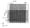
たとえば図1の様に1000素子を同時駆動する場合には、図1に示すようにフェースプレートのアノードであるITO電極を1〜1000に分割し、このアノードに分割パターンがリアプレートの電子源(図3:例えば、v004共通電極(走査電極)上の1〜1000の放出点)に対応するように位置あわせして、図17の様にパネルとして封着する。
【0046】
分離されたフェースプレート上のITO 101は同一基板上に設けた高抵抗(膜)102を介して共通電極105に束ねられ(図1)、電子源から放出された電子を加速するための高電圧が端子103及び共通電極105を介して印加される。ITO間の抵抗値は前述の高抵抗膜102の抵抗値と同等以上が好ましいが、1/100〜1/10程度以上あれば充分である。上限はない。
【0047】
しかしながら長方形をしたフェースプレートをm×lのマトリクス状に分離した場合で端にない電極が生じる場合は、端にない電極までの配線をパターン中に設ける構成をとりうる。そのような配線が必要な孤立した電極を作らないで本発明を実現する時にはm、lのどちらかは2以下にすることが接続する抵抗や取り出し電極の作製が容易にする。
【0048】
またフェースプレートのアノードの分割数はリアプレートの素子配列数に対応させて設けずに、放出点1〜4、5〜8、…の放出点のブロック毎にアノードを分割して形成し分割数を少なくすることが出来る。
【0049】
なおアノードの分割は素子配列に対して直交するように配置し画素中に分割の切れ目がない方が設計が容易だが、図5示すように斜めに交差させても効果は失われない。
【0050】
ここで、1000素子同時線順次駆動の例での適正な抵抗値を見積もると、1素子の放出電流を1〜10μAとして0.1〜1000MΩが好ましい。抵抗値の実用的な上限は電圧降下がVaの1〜数割程度以下で輝度ムラを生じない範囲で決められる。
【0051】
一般に行われている、蛍光体に1000オングストローム〜2000オングストローム程度の厚さのメタルバック処理を施した場合には加速された電子の透過率はその加速電圧が10kV程度で透過率が1に近く利用効率が高い。その10kVで加速するように設計した場合に10kVの加速電圧での電圧降下分1kVを1つの目安とすると、放出電流値により<10μA,100MΩ、1μA,1000MΩ>などの組み合わせ例が挙げられる。抵抗値の下限はDC的に流れる電流が素子破壊に対して障害がない程度に選択できる。0.1MΩ、Va=10kVでは100mAの電流が流入し、破壊が顕著になる領域である。しかし破壊は電子放出素子特性、配線抵抗値、走査電極・信号電極のスイッチング抵抗値に依存しており壊れなければ更に小さい抵抗でも良い。従って付加する抵抗値は具体的には0.01MΩ〜10GΩから選択される。1MΩ〜100MΩがより有効に機能する範囲と考えられる。
【0052】
また、たとえば、TV受像機のような高品位の要求には256階調が仕様であることから、そのレベル以下に輝度むらを抑えることが重要な意味をもつ。
【0053】
256階調すなわち0.4%の幅に抑えるために、陽極の電圧の変動幅を0.4%程度以内にする必要があるので、抵抗による電圧降下をその幅にとどめればよい。
【0054】
つまり分割された陽極に抵抗を接続し共通配線で駆動する場合には実際に電子の加速される領域での電圧が精度良くそろっていることが望ましく、共通配線で接続されていない場合には分割された電極、それぞれの電圧が揃うように調整する。
【0055】
輝度が加速電圧に対してリニアなところを利用するとして、加速電圧Vの印加された分割されたアノードの中で同時に点灯する素子の数がnの場合に、許される電圧降下量をΔVとするとΔV/Vが0.004となればいいのでアノードに接続されている抵抗がR、1素子から流れる放出電流値がIeの時
ΔV=R×n×Ieであるから
R=0.004×V/(n×Ie) で決まる。
点灯数nの最小値は2なので
R≦0.002×V/Ieである。
Va=10kVolt 、Ie=5μAではR≦4MΩとなる。
また同様にnが3であればR≦2.67MΩである。
【0056】
単純マトリクス配線を利用して素子を駆動し画像表示を行なう場合には線順次走査を行なうのが一般的である。線順次走査を行なう場合の本発明の好適な適用方法としては加速電極の分割パターンに関して走査時に同時に選択される1行の走査配線に対して垂直に配置する。そのため、分割された加速電極に接続された抵抗による電圧降下の輝度分布に及ぼす影響は1走査配線を横に分割する分割数で1走査配線に接続された電子放出素子の数を割った結果で上式のnが決まるので分割数を決めた場合により大きな抵抗Rを接続出来る。
【0057】
さらに一般的な薄膜抵抗の作成において0.4%の精度を実現するのにレーザートリミング等の手段が必要で工程の長時間化につながりコストアップの要因となる場合を鑑み、本発明では分割された加速電極に接続された抵抗の精度による輝度バラツキを補正するために分割された電極に対向した素子毎に駆動条件を異ならせることが出来る設定手段をもうけることでこの問題を解決する。
【0058】
スペーサ上の帯電防止膜は絶縁性基板の表面を導電性膜で被覆することにより、絶縁性基板表面に蓄積した電荷を除去するものであり、通常、帯電防止膜の表面抵抗が1012Ω以下であるとよい。さらに、十分な帯電防止効果を得るためには、より低い抵抗値であればよく1011Ω以下であることが好ましく、より低抵抗であれば除電効果が向上する。
【0059】
帯電防止膜を画像形成装置のスペーサに適用した場合においては、スペーサの表面抵抗は帯電防止及び消費電力からその望ましい範囲に設定される。表面抵抗の下限はスペーサにおける消費電力により制限される。低抵抗であるほどスペーサに蓄積する電荷を速やかに除去することが可能となるが、スペーサで消費される電力が大きくなる。スペーサに使用する帯電防止膜としては比抵抗が小さい金属膜よりは半導電性の材料であることが好ましい。その理由は比抵抗が小さい材料を用いた場合、表面抵抗を所望の値にするためには帯電防止膜の厚みを極めて薄くしなければならないからである。薄膜材料の表面エネルギー及び基板との密着性や基板温度によっても異なるが、一般的に102オングストローム以下の薄膜は島状となり、抵抗が不安定で成膜再現性に乏しい。
【0060】
したがって、比抵抗値が金属導電体より大きく、絶縁体よりは小さい範囲にある半導電性材料が好ましいのであるが、これらは抵抗温度係数が負の材料が多い。抵抗温度係数が負であると、スペーサ表面で消費される電力による温度上昇で抵抗値が減少し、さらに発熱し温度が上昇しつづけ、過大な電流が流れる、いわゆる熱暴走を引き起こす。しかし、発熱量すなわち消費電力と放熱がバランスした状況では熱暴走は発生しない。また、帯電防止膜材料の抵抗温度係数TCRの絶対値が小さいければ熱暴走しずらい。
【0061】
TCRが−1%の帯電防止膜を用いた条件でスペーサ1cm2 当たりの消費電力がおよそ0.1Wを越えるようになるとスペーサに流れる電流が増加しつづけ、熱暴走状態となることが実験で認められた。もちろんスペーサ形状とスペーサ間に印加される電圧Va及び帯電防止膜の抵抗温度係数により左右されるが、以上の条件から、消費電力が1cm2 あたり0.1Wを越えない表面抵抗の値は10×Va2Ω以上である。すなわち、スペーサ上に形成した帯電防止膜の表面抵抗は10×Va2Ωから1011Ωの範囲に設定されると好適である。
【0062】
上述したように絶縁性基板上に形成された帯電防止膜の膜厚は102オングストローム以上が望ましい。一方膜厚が104オングストローム以上では膜応力が大きくなって膜はがれの危険性が高まり、また成膜時間が長くなるため生産性が悪い。したがって、膜厚は102〜104オングストローム、さらには2.0×10²〜5.0×10³オングストロームであることが望ましい。比抵抗は表面抵抗と膜厚の積であり、以上に述べた好ましい範囲から、帯電防止膜の比抵抗は10-5×Va2〜107Ωcmであるとよい。さらに表面抵抗と膜厚のより好ましい範囲を実現するためには、2.0×10⁻⁵×Va2〜5.0×10⁶Ωcmとするのが良い。
【0063】
画像形成装置における電子の加速電圧Vaは100以上であり、十分な輝度を得るためには1kVの電圧を要する。Va=1kVの条件においては、帯電防止膜の比抵抗は10〜107Ωcmが好ましい範囲である。
【0064】
さらにスペーサには、アノード電極及び配線電極との良好な電気的接触を得るために、金属導電膜により帯状接触電極が好ましく形成されるとよい。すなわち、第1の導電性を有する第1の部材として帯電防止膜を設け、該帯電防止膜と、アノード電極もしくは配線電極との電気的接続を良好にする、第2の導電性を有する第2の部材として接触電極(金属導電膜)を設けるとよい。
【0065】
そこで、本発明では分割アノード電極にまたがらないようにスペーサを配置して、分割アノード電極を電気的に短絡させることをなくすようにしてもよい。
【0066】
また、本発明では分割アノード電極にまたがって配置されるスペーサに関して、分割アノード電極を電気的に短絡させることなく上記接触電極を形成するようにしてもよい。
【0067】
例えば表面抵抗が10-1〜10-2Ωに設定された接触電極は、分割アノード電極側については島状に形成する。また、帯電防止膜の表面抵抗は108から1011Ωに設定され、島状接触電極間及び分割アノード電極間の電気的短絡を防止する。さらに、島状接触電極の幅が分割アノード間距離より小さい場合にはスペーサ組み立て時のアライメントが簡単もしくは不要で、従来の姿穴治具を使った簡便な方法によりスペーサを組み立てることが可能である。また、島状接触電極のピッチをスペーサ高さよりも小さく形成した場合には、放出電子軌道に与える影響を抑制でき、望ましい効果を期待できる。
【0068】
以上のような構成のスペーサを、電流制限抵抗を介して共通接続された複数の分割アノード電極が配置され、さらに電子線の照射によって発光する発光部が形成されたフェースプレートを使用した画像形成装置に適用することにより、高輝度で歪みのない表示画像を得ることが可能で、さらに素子破壊がない高寿命の画像形成装置を作製することが可能である。
【0069】
図29、図30は、本発明のスペーサを利用した画像形成装置の構成の一例を示す模式図であり、図30は、図29におけるA−A′断面図である。
【0070】
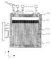
図29において、1は電子源基板であるリアプレート、2は陽極基板であるフェースプレート、3はスペーサ、4はリアプレート1の基体である基板、5は電子放出素子、6a及び6bは電子放出素子5に電圧を印加するための電極、7a(走査電極)及び7b(信号電極)は、それぞれ電極6a,6bに接続されている配線電極、8はフェースプレート2の基体である基板、9はメタルバック、10は蛍光体である。図30においては、11はスペーサに導電性を与え、帯電を緩和する帯電防止膜、12は膜11とアノード電極9及びリアプレート上の配線との電気的接続を良好にする接触電極、またdはスペーサの高さすなわちフェースプレートとリアプレート間の距離、Hはフェースプレート側の接触電極の高さ、H′はリアプレート側の接触電極の高さ、Lc はフェースプレート側の島状接触電極の幅、Pc はそのピッチ、La は分割アノード電極を構成する透明電極11の幅、Pa はそのピッチである。リアプレート1とスペーサ11を接続する例を示しているが、フェースプレート2側に絶縁性フリットを塗布してフェースプレート2とスペーサ11を接続することも可能である。
【0071】
リアプレート1は、多数の電子放出素子が基板4上に配列された電子源基板である。基板4としては、石英ガラス、青板ガラス、Na等の不純物含有量を軽減したガラス、青ガラスにSiO2 を積層したガラス基板、アルミナ等のセラミックス、及びSi基板等を用いることができるが、特に大画面表示パネルを構成する場合、青板ガラス、カリウム置換ガラス、青板ガラスに液相成長法、ゾル−ゲル法、スパッタ法等によりSiO2 を積層したガラス基板等が、比較的低コストであり、好ましく用いることができる。電子放出素子5として、ここでは、表面伝導型電子放出素子を用いている。
【0072】
図31はこの構成例に係わる画像形成装置の構成図、図32はこの構成例に係わる画像形成装置の電子源の製法図である。図31及び図32において、図29、図30に示した部位と同じ部位には図29、図30に付した符号と同一の符号を付している。図32において31は導電性薄膜、32は電子放出部である。導電性薄膜31には、たとえば、10オングストロームより500オングストロームの範囲の膜厚の導電性微粒子で構成された微粒子膜が好ましく用いられる。導電性薄膜31を構成する材料として、種々の導電体、ないし半導体を用いることができるが、特にPd、Pt、Ag、Au等の貴金属元素を含む有機化合物を加熱焼成して得られるPd、Pt、Ag、Au、PdO等が好ましく用いられる。電子放出部32は、導電性薄膜31の一部に形成された高抵抗の亀裂により構成され、その内部には、導電性薄膜31を構成する材料の元素、及び炭素、炭素化合物を含有する数オングストロームから数百オングストロームの範囲の粒径の導電性微粒子が存在する場合もある。
【0073】
電極6a,6bとしては、一般的な導体材料を用いることができる。これは例えばNi、Cr、Au、Mo、W、Pt、Ti、Al、Cu、Pd等の金属或いは合金及びPd、Ag、Au、RuO2 、Pd−Ag等の金属或いは金属酸化物とガラス等から構成される印刷導体、In2 O3 −SnO2 等の透明導電体及びポリシリコン等の半導体導体材料等から適宜選択することができる。
【0074】
電子放出素子5の配列については、種々のものが採用できる。ここで説明しているのは単純マトリクス配置と称される配列で、電子放出素子5をX方向及びY方向に行列状に複数個配し、同じ行に配された複数の電子放出素子5の電極の一方6aを、X方向の配線7aに共通に接続し、同じ列に配された複数の電子放出素子5の電極の他方6bを、Y方向の配線7bに共通に接続したものである。X方向配線電極7a、Y方向配線電極7b共に真空蒸着法、印刷法、スパッタ法等を用いて形成された導電性金属等で構成することができる。配線の材料、膜厚、巾は適宜設計される。また、層間絶縁層14は、ガラス、セラミック等を真空蒸着法、印刷法、スパッタ法等を用いて形成された絶縁体層である。例えば、X方向配線7aを形成した基板4の全面或いは一部に所望の形状で形成され、特に、X方向配線7aとY方向配線7bの交差部の電位差に耐え得るように、膜厚、材料、製法が、適宜設定される。X方向配線7aには、X方向に配列した電子放出素子5の行を選択するための走査信号を印加する、不図示の走査信号印加手段が接続される。一方、Y方向配線7bには、Y方向に配列した電子放出素子5の各列を入力信号に応じて、変調するための不図示の変調信号発生手段が接続される。各電子放出素子に印加される駆動電圧は、当該素子に印加される走査信号と変調信号の差電圧として供給される。
【0075】
上記構成においては、単純マトリクス駆動により、個別の素子を選択し、独立に駆動可能とすることができる。
【0076】
このほかに、並列に配置した多数の電子放出素子の個々を両端で接続し、電子放出素子の行を多数個配し(行方向と呼ぶ)、この配線と直交する方向(列方向と呼ぶ)で、該電子放出素子の上方に配した制御電極(グリッドとも呼ぶ)により、電子放出素子からの電子を制御駆動するはしご状配置のもの等があるが、本発明は特にこれらの配置によって限定されるものではない。
【0077】
フェースプレート2は、基板8の表面にメタルバック9と蛍光体膜10等を形成した陽極基板である。基板8としては、透明であることは言うまでもないが、リアプレート用基板4と同様の機械強度、熱物性を有するものが好ましく、大画面表示パネルを構成する場合、青板ガラス、カリウムガラス、青板ガラスに液相成長法、ゾル−ゲル法、スパッタ法等によりSiO2 を積層したガラス基板等が、好ましく用いることができる。
【0078】
メタルバック9は、電圧降下をできるだけ小さく抑えるためにY方向配線7bに平行、X方向配線7aに垂直に配置されるよう、フォトリソグラフィーによって分割パターニングされ、さらに分割列毎に100MΩ程度の電流制限抵抗を介して共通接続された取り出し部分に不図示の外部電源から正の高電圧Vaが印加される。このとき、分割アノード電極の幅La 及びピッチPa は画像形成装置における素子数及びX方向配線側の素子ピッチPx 等によっても異なるが、概ね以下のように規定される。
【0079】
Pa =n・Px (n∈N|n<100)
10-6m≦Pa −La ≦10-4m
こうして電子放出素子5より放出された電子はフェースプレート2へ引きつけられ、加速されて蛍光体膜10に照射される。このとき、入射電子が蛍光体膜10を発光させるのに十分なエネルギーをもっていれば、そこに輝点を得ることができる。一般に、カラーTV用CRTに用いられている蛍光体では、数kVから数10kVの加速電圧で電子を加速して照射して良好な輝度と発色を得ている。CRT用の蛍光体は、比較的安価でありながら非常に高い性能を有するため、本発明においても好ましく用いることができる。アノード電極としてメタルバックを採用する場合、蛍光体の発光のうちリアプレート1側への光をフェースプレート2側へ鏡面反射させることにより輝度を向上させること、外囲器内で発生した負イオンの衝突によるダメージから蛍光体を保護するという更なる効果もある。アノード電極として透明電極を用いる場合で、かつ支持部材と透明電極を電気的に接続する場合は、透明電極と支持部材の間に蛍光体が介在するが、外囲器内外の圧力差等によって蛍光体はつぶされる為、電気的な接続は実現できる。また透明電極と支持部材の間には蛍光体を配置しない様にしてもよい。
【0080】
図31において、外枠13は、リアプレート1及びフェースプレート2と接続されており、外囲器を形成している。外枠13とリアプレート1及びフェースプレート2との接続は、リアプレート1、フェースプレート2、外枠13を構成する材質にもよるが、一例としてガラスを用いた場合、ガラスフリットを用いて融着することができる。スペーサ11は、耐大気圧支持とリアプレート1とフェースプレート2間の距離dを略均等にする目的がある。この距離dは、上述の高電圧Vaによる真空中の放電を起こさない程度に大きくなければならない。一方、電子放出素子5からの放出電子は有限の拡がり角をもっているため、あまり大きな距離をとると、隣り合う画素との重なりを生じ、混色やコントラスト低下を生じる場合がある。したがって、上記数kVから数10kVのVaに対して、数百μmから数mm程度の距離d、すなわちスペーサ高さに設定されるのが望ましい。
【0081】
以下、本発明のスペーサの作製法の一例を述べる。
【0082】
まず、洗浄したガラス基板に真空蒸着法、スパッタ法、印刷法、引き上げ法等により導電性金属で接触電極を形成する。フェースプレート側の島状接触電極のスケールに関して、図30における符号を用いると、以下の条件を満足することが望ましい。
【0083】
第一に如何なるアライメントによっても島状接触電極が複数の分割アノードラインを短絡しない条件、
Lc <Pa −La …(1)
第二に島状接触電極によって素子間で輝点のバラツキが生じるような電界ムラを抑制する条件、
Pc ≦Px ≦Pa …(2)
H≪d …(3)
リアプレート側の帯状接触電極のスケールに関しては、第二の条件を満足することが望ましい。
【0084】
H′≪d …(4)
このようにして接触電極が形成されたスペーサは、さらに真空蒸着法、スパッタ法、印刷法、引き上げ法等によって導電性を有する帯電防止膜が形成される。
【0085】
この帯電防止膜の表面抵抗Rsは、
108 Ω<Rs<1011Ω
なる範囲に望ましく設定される。抵抗の下限は、分割アノード電極間の短絡抑止、消費電力の抑制等から規定され、上限はスペーサの帯電防止効果が認められる範囲に規定される。
【0086】
以上を満足すれば、スペーサとフェースプレートとの位置合わせをせずに、放電耐性及び放出電子軌道に位置的なバラツキがない均一な画像形成装置を作製できる。
【0087】
【実施例】
以下、実施例を用いて本発明をさらに詳しく説明する。本発明の理解の容易化のために、参考例についても説明を行う。
【0088】
実施例及び参考例で示す図面中XY軸に対してX方向に平行に走査配線、Y方向に平行に信号配線が有するものとする。
【0089】
[参考例1]
図17で述べた電子放出素子を利用した画像形成装置を試作した。図3に示すようにリアプレートのマルチ電子源はマトリクス配線されたSEC電子源(後に詳細に述べる)である。図3の300は各電子放出素子を示す。この電子源は共通配線単位の1000素子ごとに線順次駆動される。放出点は1000×500である。
【0090】
一方、図1に示すように、フェースプレートは、ガラス基板にベタでITO膜を形成した後、230μmピッチ(1000ライン分)にフォトリソグラフィー工程で分離(101)し、片側を100MΩの抵抗体(パターニングしたNiO膜(102))を介して束ねて高電圧を端子103から印加出来るようにした。
【0091】
次に図2に示すように分離したITO上に蛍光体ZnS(Cuドープ)を塗布焼成し201,202、冷陰極マルチ電子源(リアプレート)に対して陽極高電圧を印加するフェースプレートとした。
【0092】
リアプレートの共通配線v001,v002,…とフェースプレートのITO分離配線101とは直交(交差)するよう配置した。本参考例では共通配線v001,v002,…v500は走査配線であり、各配線上の1000個の素子は同時に電子を放出する可能性があるが、同時に駆動される可能性のある素子が並ぶ方向(走査配線の方向)と非平行にアノード電極を分割することにより、各アノード電極に流れる電流の変化の範囲を抑制している。
【0093】
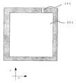
図1のフェースプレートと図3のリアプレート間を2mmにし、高電圧Va:5kVを印加した。線順次駆動はTVレートで1ライン30μsecでスクロールした。リアプレート、フェースプレート間の放電の影響を調べるために、画像形成装置内の真空度を落とす(悪くする)ことにより計測を行った。外部回路の測定及び蛍光体の輝点をCCDにより検出することにより放電は2回/時間程度観測されたが、画素の大幅な輝度劣化は認められなかった。比較のため試作したフェースプレートのITOを分離しない(図4)場合は縦、横の配線に沿って画素の大幅な輝度劣化が認められた。
【0094】
図4において401はITO膜、403は取り出し電極を示す。
【0095】
以下、本発明に使用した表面伝導型(SCE)電子放出素子について説明する。図12は、本発明を適用可能な平面型表面伝導型電子放出素子の構成を示す模式図であり、図12(a)は平面図、図12(b)は断面図である。図12において311は基板、312と313は素子電極、314は導電性薄膜、315は電子放出部である。
【0096】
基板311としては、石英ガラス、Na等の不純物含有量を減少したガラス、青板ガラス、青板ガラスにスパッタ法等により形成したSiO2 を積層したガラス基板及びアルミナ等のセラミックス及びSi基板等を用いることができる。対向する素子電極312,313の材料としては、一般的な導体材料を用いることができる。これは例えばNi、Cr、Au、Mo、W、Pt、Ti、Al、Cu、Pd等の金属或いは合金及びPd、Ag、Au、RuO2 、Pd−Ag等の金属或いは金属酸化物とガラス等から構成される印刷導体、In2 O3 −SnO2等の透明導電体及びポリシリコン等の半導体導体材料等から適宜選択することができる。
【0097】
素子電極間隔SL、素子電極長さSW、導電性薄膜314の形状等は、応用される形態等を考慮して設計される。素子電極間隔SLは、好ましくは数千オングストロームから数百マイクロメートルの範囲とすることができ、より好ましくは、素子電極間に印加する電圧等を考慮して数マイクロメートルから数十マイクロメートルの範囲とすることができる。
【0098】
素子電極長さSWは、電極の抵抗値、電子放出特性を考慮して、数マイクロメートルから数百マイクロメートルの範囲とすることができる。素子電極312,313の膜厚dは、数百オングストロームから数マイクロメートルの範囲とすることができる。尚、図12に示した構成だけでなく、基板311上に、導電性薄膜314、対向する素子電極312,313の順に積層した構成とすることもできる。
【0099】
導電性薄膜314には、良好な電子放出特性を得るために、微粒子で構成された微粒子膜を用いるのが好ましい。その膜厚は、素子電極312,313へのステップカバレージ、素子電極312,313間の抵抗値及び後述するフォーミング条件等を考慮して適宜設定されるが、通常は、数オングストロームから数千オングストロームの範囲とするのが好ましく、より好ましくは10オングストロームより500オングストロームの範囲とするのが良い。その抵抗値は、Rsが102から107Ω/□の値である。なおRsは、厚さがt、幅がwで長さがlの薄膜の抵抗Rを、R=Rs(l/t×w)とおいたときに現れる。ここでは、フォーミング処理については、通電処理を例に挙げて説明するが、フォーミング処理はこれに限られるものではなく、膜に亀裂を生じさせて高抵抗状態を形成する処理であれば通電処理以外のものであっても良い。
【0100】
導電性薄膜314を構成する材料は、Pd、Pt、Ru、Ag、Au、Ti、In、Cu、Cr、Fe、Zn、Sn、Ta、W、Pb等の金属、PdO、SnO2 、In2 O3 、PbO、Sb2 O3 等の酸化物、HfB2 、ZrB2 、LaB6 、CeB6 、YB4 、GdB4 等の硼化物、TiC、ZrC、HfC、TaC、SiC、WC等の炭化物、TiN、ZrN、HfN等の窒化物、Si、Ge等の半導体、カーボン等の中から適宜選択される。
【0101】
ここで述べる微粒子膜とは、複数の微粒子が集合した膜であり、その微細構造は、微粒子が個々に分散配置した状態あるいは微粒子が互いに隣接、あるいは重なり合った状態(いくつかの微粒子が集合し、全体として島状構造を形成している場合も含む)をとっている。微粒子の粒径は、数オングストロームから数千オングストロームの範囲、好ましくは、10オングストロームから200オングストロームの範囲である。なお、本明細書では頻繁に「微粒子」という言葉を用いるので、その意味について説明する。
【0102】
小さな粒子を「微粒子」と呼び、これよりも小さいものを「超微粒子」と呼ぶ。「超微粒子」よりもさらに小さく原子の数が数百個程度以下のものを「クラスター」と呼ぶことは広く行われている。
【0103】
しかしながら、それぞれの境は厳密なものではなく、どの様な性質に注目して分類するかにより変化する。また「微粒子」と「超微粒子」を一括して「微粒子」と呼ぶ場合もあり、本明細書中での記述はこれに沿ったものである。「実験物理学講座14 表面・微粒子」(木下是雄編、共立出版 1986年9月1日発行)では次のように記述されている。
【0104】
「本稿で微粒子と言うときにはその直径がだいたい2〜3μm程度から10nm程度までとし、特に超微粒子というときは粒径が10nm程度から2〜3nm程度までを意味することにする。両者を一括して単に微粒子と書くこともあってけっして厳密なものではなく、だいたいの目安である。粒子を構成する原子の数が2個から数十〜数百個程度の場合はクラスターと呼ぶ。」(195ページ22〜26行目)
付言すると、新技術開発事業団の“林・超微粒子プロジェクト”での「超微粒子」の定義は、粒径の下限はさらに小さく、次のようなものであった。「創造科学技術推進制度の“超微粒子プロジェクト”(1981〜1986)では、粒子の大きさ(径)がおよそ1〜100nmの範囲のものを“超微粒子”(ultra fine particle)と呼ぶことにした。すると1個の超微粒子はおよそ100〜108個くらいの原子の集合体という事になる。原子の尺度でみれば超微粒子は大〜巨大粒子である。」
(「超微粒子 創造科学技術」林主税、上田良二、田崎明編;三田出版 1988年2ページ1〜4行目)「超微粒子よりさらに小さいもの、すなわち原子が数個〜数百個で構成される1個の粒子は、ふつうクラスターと呼ばれる」(同書2ページ12〜13行目)
上記のような一般的な呼び方をふまえて、本明細書において「微粒子」とは多数の原子・分子の集合体で、粒径の下限は数オングストローム〜10オングストローム程度、上限は数μm程度のものを指すこととする。
【0105】
電子放出部315は、導電性薄膜314の一部に形成された高抵抗の亀裂により構成され、導電性薄膜314の膜厚、膜質、材料及び後述する通電フォーミング等の手法等に依存したものとなる。電子放出部315の内部には、数オングストロームから数百オングストロームの範囲の粒径の導電性微粒子が存在する場合もある。この導電性微粒子は、導電性薄膜314を構成する材料の元素の一部、あるいは全ての元素を含有するものとなる。電子放出部315及びその近傍の導電性薄膜314には、炭素及び炭素化合物を有することもできる。
【0106】
上述の表面伝導型電子放出素子の製造方法としては様々な方法があるが、その一例を図13に模式的に示す。
【0107】
以下、図13を参照しながら製造方法の一例について説明する。図13においても、図12に示した部位と同じ部位には図12に付した符号と同一の符号を付している。
【0108】
1)基板311を洗剤、純水及び有機溶剤等を用いて十分に洗浄し、真空蒸着法、スパッタ法等により素子電極材料を堆積後、例えばフォトリソグラフィー技術を用いて基板311上に素子電極312,313を形成する(図13(a))。
【0109】
2)素子電極312,313を設けた基板311に、有機金属溶液を塗布して、有機金属薄膜を形成する。有機金属溶液には、前述の導電性薄膜314の材料の金属を主元素とする有機金属化合物の溶液を用いることができる。有機金属薄膜を加熱焼成処理し、リフトオフ、エッチング等によりパターニングし、導電性薄膜314を形成する(図13(b))。ここでは、有機金属溶液の塗布法を挙げて説明したが、導電性薄膜314の形成法はこれに限られるものでなく、真空蒸着法、スパッタ法、化学的気相堆積法、分散・塗布法、ディッピング法、スピンナー法等を用いることもできる。
【0110】
3)つづいて、フォーミング工程を施す。このフォーミング工程の方法の一例として通電処理による方法を説明する。素子電極312,313間に、不図示の電源を用いて通電を行うと、導電性薄膜314の部位に構造の変化した電子放出部5が形成される(図13(c))。通電フォーミングによれば導電性薄膜314に局所的に破壊、変形もしくは変質等の構造の変化した部位が形成される。該部位が電子放出部315を構成する。通電フォーミングの電圧波形の例を図14に示す。
【0111】
電圧波形は、パルス波形が好ましい。これにはパルス波高値を定電圧としたパルスを連続的に印加する図14(a)に示した手法とパルス波高値を増加させながら、電圧パルスを印加する図14(b)に示した手法がある。
【0112】
図14(a)におけるT1及びT2は電圧波形のパルス幅とパルス間隔である。通常T1は1マイクロ秒〜10ミリ秒、T2は、10マイクロ秒〜100ミリ秒の範囲で設定される。三角波の波高値(通電フォーミング時のピーク電圧)は、表面伝導型電子放出素子形態に応じて適宜選択される。このような条件のもと、例えば、数秒から数十分間電圧を印加する。パルス波形は三角波に限定されるものではなく、矩形波など所望の波形を採用することができる。
【0113】
図14(b)におけるT1及びT2は、図14(a)に示したのと同様とすることができる。三角波の波高値(通電フォーミング時のピーク電圧)は、例えば0.1Vステップ程度づつ、増加させることができる。
【0114】
通電フォーミング処理の終了は、パルス間隔T2中に、導電性薄膜2を局所的に破壊、変形しない程度の電圧を印加し、電流を測定して検知することができる。例えば0.1V程度の電圧印加により流れる素子電流を測定し、抵抗値を求めて1MΩ以上の抵抗を示した時、通電フォーミングを終了させる。
【0115】
4)フォーミングを終えた素子には活性化工程と呼ばれる処理を施すのが好ましい。活性化工程とは、この工程により素子電流If、放出電流Ieが著しく変化する工程である。
【0116】
活性化工程は、例えば有機物質のガスを含有する雰囲気下で、通電フォーミングと同様に、パルスの印加を繰り返すことで行うことができる。この雰囲気は、例えば油拡散ポンプやロータリーポンプなどを用いて真空容器内を排気した場合に雰囲気内に残留する有機ガスを利用して形成することができる他、イオンポンプなどにより一旦十分に排気した真空中に適当な有機物質のガスを導入することによっても得られる。このときの好ましい有機物質のガス圧は、前述の応用の形態、真空容器の形状や有機物質の種類などにより異なるため場合に応じ適宜設定される。適当な有機物質としては、アルカン、アルケン、アルキンの脂肪族炭化水素類、芳香族炭化水素類、アルコール類、アルデヒド類、ケトン類、アミン類、フェノール、カルボン、スルホン酸等の有機酸類等を挙げることが出来、具体的には、メタン、エタン、プロパンなどCnH2n+2で表される飽和炭化水素、エチレン、プロピレンなどCnH2n等の組成式で表される不飽和炭化水素、ベンゼン、トルエン、メタノール、エタノール、ホルムアルデヒド、アセトアルデヒド、アセント、メチルエチルケトン、メチルアミン、エチルアミン、フェノール、蟻酸、酢酸、プロピオン酸等が使用できる。この処理により、雰囲気中に存在する有機物質から、炭素あるいは炭素化合物が素子上に堆積し、素子電流If、放出電流Ieが著しく変化するようになる。活性化工程の終了判定は、素子電流Ifと放出電流Ieを測定しながら適宜行う。なお、パルス幅、パルス間隔、パルス波高値などは適宜設定される。
【0117】
炭素及び炭素化合物とは、例えばグラファイト(いわゆるHOPG,PG,GCを包含する。HOPGはほぼ完全なグラファイトの結晶構造、PGは結晶粒が200オングストローム程度で結晶構造がやや乱れたもの、GCは結晶粒が20オングストローム程度になり結晶構造の乱れがさらに大きくなったものを指す。)、非晶質カーボン(アモルファスカーボン及び、アモルファスカーボンと前記グラファイトの微結晶の混合物を指す)であり、その膜厚は、500オングストローム以下の範囲とするのが好ましく、300オングストローム以下の範囲とすることがより好ましい。
【0118】
5)このような工程を経て得られた電子放出素子は、安定化工程を行うことが好ましい。この工程は、真空容器内の有機物質排気する工程である。真空容器内の圧力は、1〜3×10⁻⁷Torr以下が好ましく、さらに1×10⁻⁸Torr以下が特に好ましい。真空容器を排気する真空排気装置は、装置から発生するオイルが素子の特性に影響を与えないように、オイルを使用しないものを用いるのが好ましい。具体的には、ソープションポンプ、イオンポンプ等の真空排気装置を挙げることが出来る。さらに真空容器内を排気するときには、真空容器全体を加熱して、真空容器内壁や電子放出素子に吸着した有機物質分子を排気しやすくなるのが好ましい。このときの加熱条件は、80〜200℃で5時間以上が望ましいが、特にこの条件に限るものではなく、真空容器の大きさや形状、電子放出素子の構成などの諸条件により適宜選ばれる条件により行う。
【0119】
安定化工程を行った後の駆動時の雰囲気は、上記安定化処理終了時の雰囲気を維持するのが好ましいが、これに限るものではなく、有機物質が十分除去されていれば、真空度自体は多少低下しても十分安定な特性を維持することが出来る。このような真空雰囲気を採用することにより、新たな炭素あるいは炭素化合物の堆積を抑制でき、結果として素子電流If、放出電流Ieが安定する。
【0120】
[参考例2]
本参考例では、図15に示すようにフェースプレートガラス基板上に導電性ブラックストライプ;BS(カーボン60%、水ガラス成分40%を分散したもの)をスクリーン印刷した(1001)。幅100μm、ピッチ230μm、厚み10μmとした。抵抗値は150Ω/□である。
【0121】
さらに高抵抗体としてRuO2 を印刷した。抵抗値は幅100μm長さ750μmで10MΩであった(1002)。次にCRT用蛍光体P22をR、G、BをBS間にストライプ状に10μm厚で塗布、焼成した。続いてAlのメタルバックを施した(1003)。アクリル系の樹脂をディッピングで成形後1000オングストロームのAlを蒸着、焼成する。Al側からレーザ加工によりAl膜を分離することにより目的のフェースプレートを得た。
【0122】
本素子を参考例1のリアプレートと参考例1と同様に封着し、パネルを形成し同様の耐放電テストを行ったところ、放電は2〜5回/時間程度観測されたが画素の大幅な輝度劣化は認められず、Al膜を分離しないものと比較して放電ダメージを顕著に減少させる効果が認められた。又試験的に1ライン、10ライン、100ライン毎に分離幅を変えてテストしたところ細かい分離幅の方が、放電ダメージが小さく有効である事がわかった。(図15はこのレーザ加工の様子を模式図的に示したものである。)
具体的には1ライン、10ラインの分離領域では画素の大幅な輝度劣化はなかったが100ライン部では数画素にわたる劣化が(輝度低下が)認められた。
【0123】
比較例として行ったAlを分離しないパネルでは参考例1と同様の配線にそって画素の大幅な輝度劣化が生じた。
【0124】
[参考例3]
本参考例では図16(a)、図16(b)に示すように、参考例2で行った樹脂ディッピングの後Al斜め蒸着を行った図16において1105は蛍光体、1106はフェースプレートを構成するガラス基板、1107は蒸着Al膜である。
【0125】
BS1101の高さはAlビーム1102の影を形成するよう25μmとした。ここにAlビーム1102を斜め方向からあてることにより、分割されたAl膜1107を設けた。焼成後1ライン毎の素子分離が大部分(90%以上)が100MΩ以上である事を確認、作成されたフェースプレートとリアプレートとを封着し、素子活性化後、参考例1と同様の耐放電テストを行ったところ、Al膜を分離しないサンプルと比較し放電に対して有意な改善が認められた。すなわち放電回数は〜3回/時間であったが、放電にともなう大幅な輝度劣化は認められなかった。比較例サンプルでは参考例2で示したものと同じように配線にそった画素の大幅な輝度劣化が発生した。完全にアノード(Alのメタルバック)分離が出来なくても、ある程度有効である事が実験からも確認出来た。これは不完全な素子分離によっても、蓄積電荷容量が減少している効果によるものと考えられる。
【0126】
[参考例4]
本参考例ではフェースプレートを構成するガラス基板上に導電性ブラックストライプ;BS(カーボン60%、水ガラス成分40%を分散したもの)をスクリーン印刷した。本参考例では導電性ブラックストライプがアノード電極を兼ねる。幅100μm、ピッチ230μm、厚み10μmとした。抵抗値は150Ω/□である。高抵抗体としてRuO2 を印刷した。抵抗値は幅100μm長さ750μmで10MΩであった。次に低抵抗化処理済 GREEN蛍光体(ZnS、Cu doped In2 O3 添加、比抵抗〜109Ωcm)を10μm厚で表示部全面に形成した。導電性BS間の抵抗値はRuO2 の抵抗値10MΩと隣接BS間の導電性蛍光体抵抗〜300MΩの並列抵抗で分離されている。参考例1と同様に画像形成装置を形成し、放電による劣化特性を比較したところ、参考例1のITOパターンによる素子分離の場合と同様な有効な結果を得た。低抵抗化処理をしないZnSを用いた場合は1012Ωcmの比抵抗であり、若干のチャージアップ現象がみられたが、放電耐性は効果が認められた。このように初めに述べたように、フェースプレート陽極上で1〜100MΩ程度の分離ができれば、本発明が有効であることが実証された。
【0127】
[参考例5]
本参考例ではフェースプレートを構成するガラス基板上に透明導電性膜をシート抵抗値が100KΩ/□になるようにSbをドープしたIn2 O3 で形成した。
【0128】
参考例1のようにストライプ状にパターニングし、参考例1と同様分割されたアノード1つあたりの抵抗を100MΩとした後、取り出し部にAg印刷電極103、蛍光体(不図示)を形成、焼成した(図1)。ただし本参考例ではアノードが有意な抵抗を有しており、アノード自体がアノードが抵抗体を介して接続される際の抵抗体を兼ねるので、別個に設けた抵抗体102はない。
【0129】
参考例1と同じ封着工程でリアプレートと対向させてパネル化しディスプレーとした。放電に対する耐性は図4に示す比較用ベタ低抵抗ITOサンプルより優れており、電圧降下による輝度ムラも実用に耐える程度であった。線順次駆動実験中の同時放出電流はΣIe=0〜1mAであり、DC印加電圧の電圧降下による輝度ムラは許容出来る範囲であった。
【0130】
[参考例6]
本参考例では電子放出素子として電界放出型電子放出素子(FE)を用いた。
【0131】
図6に示すように、リアプレートを構成するガラス基板707に、陰極膜706、アモルファスSi抵抗膜701、SiO2 絶縁膜702、ゲート膜703を順次積層する。続いて、ドライエッチングにより2μmの穴を開けた後、SiO2 層のみ選択的にドライエッチングで除去した。つぎに、ゲート上にNiカソード配線膜を形成後、冷陰極材のMo704を回転斜方蒸着により成膜した。ゲート上のMo膜はNiのリフトオフにより除去しFE電子源を形成した。各電子放出ユニットは図6(a)のような構造をしている。
【0132】
この電子放出素子を〜2000個を1画素として1000×500の陰極側電子放出源をリアプレートとした。陽極側は[参考例1]の方法で蛍光体を塗布したフェースプレートを用い、リアプレートと封着してディスプレーパネルを形成した。
【0133】
フェースプレート、リアプレート間に600V電圧を印加、リアプレートはカソード配線、ゲート電極で選択的に必要画素を駆動することで平面ディスプレーを実現した。陽極のITOを分割しなかった(図4)のフェースプレートを用いたパネルはゲート電極、Mo陰極先端部の放電による劣化が顕著であったが、(図1)のITO分割したフェースプレートを用いた方は放電劣化が著しく軽減され、本発明の有効性が実証された。すなわちITOを分割した場合は一定時間駆動中の放電による画素の輝度の大幅な劣化はなかった。比較例では放電により輝度が50%以下になった画素が20点見られた。
【0134】
[参考例7]
本参考例のフェースプレート構造について述べる。参考例1と同様にガラス基板にITO膜を形成、230μmピッチ(1500ライン分)に分離し、片側を100MΩの抵抗体(スクリーン印刷によりRuO2 を分離形成)を介して束ねて高電圧を印加出来るようにした(図1)。
【0135】
次に分離したITO上の分離溝毎に絶縁性ブラックストライプを印刷、次に、分離したITOストライプ101上に各色RGB蛍光体(P22)を周期的に塗布焼成した。Alメタルバック形成後BS上に沿ってレーザ加工しAlメタルバックも分離し、後述する冷陰極マルチ電子源(リアプレート)に対して陽極高電圧を印加するカラーフェースプレートとした(図1)。
【0136】
リアプレートは1500×500のSCE電子放出素子を形成し、図3に示す共通配線とフェースプレートのITO分離配線とは直交(交差)するよう、かつ電子放出素子とRGB蛍光体が対向するようにアライメント封着した。
【0137】
フェースプレートとリアプレートとの間隔は3mmとし高電圧Va;8kVを印加した。線順次駆動はTVレートで1ライン30μsecでスクロールした。リアプレート、フェースプレート間の放電は外部回路の測定及び蛍光体の輝点をCCDにより検出することにより行い、駆動初期は〜5回/時間程度観測されたが、リアプレート側の素子劣化は認められなかった。すなわち画素の輝度の大幅な劣化は認められなかった。比較のため試作したフェースプレートのITOを分離しない場合は放電に因る画素の輝度の大幅な劣化が横、縦の配線に沿って認められる場合があった。
【0138】
[参考例8]
本参考例でのフェースプレート構造について述べる。
【0139】
図20に示すように、フェースプレートガラス基板上にAgの取り出し配線3箇所103を印刷した。縦横の絶縁性ブラックストライプをスクリーン印刷した。横幅100μm、横ピッチ282μm、縦幅300μm、縦ピッチ842μm、厚み10μmとした。取り出し配線を外付け抵抗3つを介して電源V1、V2及びV3に接続し加速電圧が掛けられるようにした。それぞれの抵抗値は10.1MΩと10.3MΩ、10.4MΩであった。
【0140】
次にCRT用蛍光体P22をR、G、BをBS間にストライプ状に15μm厚で塗布、焼成した。続いてAlメタルバックを形成した。(アクリル系の樹脂をディッピングで形成後1000オングストロームのAl蒸着、焼成する。)本フェースプレートは約16:9の表示エリアをもっている。
【0141】
左右から320個目の縦のブラックストライプにそって2本Al側からレーザ加工によりAl膜を分離することにより目的のフェースプレートを得た。リアプレートは2556×480のSCE電子放出素子を形成した。
【0142】
電子放出素子とRGB蛍光体が対向するようにフェースプレートとリアプレートをアライメントし封着した。フェースプレートとリアプレート間隔は3mmとし高電圧Va;8kVを印加した。線順次駆動はTVレートで1ライン30μsecでスクロールした。
【0143】
全面を発光させCCDで計測したところ抵抗値のバラツキと同様に一番抵抗値の高い抵抗が接続された取り出し電極高圧を供給する分割された加速電極に対応した面の輝度が暗かったが、高圧電源の出力を調整し駆動したところ分割電極に対応した輝度差は計測誤差以内にすることが出来た。
【0144】
リアプレート、フェースプレート間の放電は外部回路の測定及び蛍光体の輝点をCCDにより検出することにより駆動初期は〜5回/時間程度観測されたが、リアプレート側の素子劣化は認められなかった。また、NTSC画像等の4:3の縦横比率を画面中央に出す場合に外側の領域の高圧を0.3kV落としたところ放電回数が減り〜2回/時間程度観測されたが、高圧を落とした領域では放電は観測されなかった。また放電による画素の輝度の劣化は認められなかった。
【0145】
[参考例9]
本参考例ではリアプレートのマルチ電子源はマトリクス配線されたSCE電子源である。この電子源は共通配線単位の1500素子ごとに線順次駆動される。放出点は1500×500である。
【0146】
一方、図21に示すように、フェースプレートは、ガラス基板2101に2分割されたITO膜2102を形成、取り出し電極103を形成し10kΩの外付け抵抗(不図示)を介し高電圧を印加出来るようにした。
【0147】
次にITO上に縦横に絶縁性ブラックストライプを幅100μm、ピッチ230μm、厚み10μmと印刷した(不図示)。次にCRT用蛍光体P22に導電性を付加したもの(In2 O3 添加、比抵抗〜109Ωcm)各色R、G、BをBS間にストライプ状に10μm厚で塗布、焼成した(2103)。続いてAlのメタルバックを施した(2104)。(アクリル系の樹脂をディッピングで形成後1000オングストロームのAlを蒸着、焼成する。)Alメタルバック形成後BS上に沿ってレーザ加工しAl膜を分離することで冷陰極マルチ電子源(リアプレート)に対して陽極高電圧を印加するカラーフェースプレートとした。
【0148】
図22に本参考例のフェースプレートの模式的な断面図を示す。
【0149】
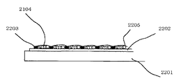
ガラス基板2201、ITO膜2202、ブラックストライプ2203、蛍光体2204、メタルバック2205である。画素ごとのメタルバックはブラックストライプと蛍光体の抵抗で絶縁分離されており放電時の電流は1画素分の大きさのメタルバックの容量成分にたまるわずかな電荷で決まる電流は流れてしまうが電源から供給される分は蛍光体の抵抗及び外付け抵抗で制限されるので素子破壊にいたるような電流は流れない。導電性のない蛍光体を用いたフェースプレートも作製したが、帯電により若干の輝度低下が見られたが放電時の電流抑制の効果は同様にあった。
【0150】
リアプレートとフェースプレートは電子放出素子とRGB蛍光体が対向するようにアライメントし封着した。フェースプレートとリアプレート間隔は3mmとし高電圧Va;8kVを印加した。線順次駆動はTVレートで1ライン30μsecでスクロールした。リアプレート、フェースプレート間の放電は外部回路の測定及び蛍光体の輝点をCCDにより検出することにより駆動初期は〜8回/時間程度観測されたが、画素の大幅な輝度劣化は認められなかった。比較のため試作したフェースプレートのメタルバックを分離しない場合は放電に因る縦、横の配線に沿って画素の大幅な輝度劣化が認められた。
【0151】
[参考例10]
本参考例ではリアプレートのマルチ電子源はマトリクス配線されたSCE電子源である。この電子源は共通配線単位の2556素子ごとに線順次駆動される。放出点は2556×480である。
【0152】
一方、フェースプレート構造の部分拡大図を図23に示す。
【0153】
フェースプレートを構成するガラス基板2301上にAgの取り出し配線2303を印刷した。絶縁性ブラックストライプ2305をスクリーン印刷した。横幅100μm、横ピッチ282μm、厚み10μmとした。高抵抗体としてRuO2 を印刷した(2302)。抵抗値は幅100μm、長さ750μmであり100MΩであった。
【0154】
次にCRT用蛍光体P22をR、G、BをBS間にマトリクス状に15μm厚で塗布、焼成した。続いてAlメタルバックを形成した(2304)。(アクリル系の樹脂をディッピングで形成後1000オングストロームのAlを蒸着、焼成する。)ブラックストライプにそってAl側からレーザ加工によりAl膜を分離する。
【0155】
次に走査ラインに垂直に2分割することにより図24に示す様な目的のフェースプレートを得た。図24はフェースプレートとリアプレートを重ね合せた図である。すなわち、それぞれの電子放出素子に対応した幅で加速電極であるメタルバックがストライプ状に分離されたフェースプレートである。
【0156】
リアプレートの共通配線v001,v002,…とフェースプレートの分離されたアルミのメタルバック2304とが図の通り、直交(交差)するよう配置した。
【0157】
表示パネルの配線は、端子Dx1からDxm(m=2556)及びDy1からDyn(n=480)を介して外部の電気回路と接続されている。走査回路2306の出力はそれぞれリアプレートの端子Dy1からDynに接続され共通配線v001,v002を1ライン30μsec、60Hzでスクロールし駆動する。
【0158】
走査回路2306について説明する。同回路は、内部にn個のスイッチング素子を備えるもので、各スイッチング素子は、図示せぬ直流電圧源の2つの出力電圧VsもしくはVsnのいずれか一方を選択し、表示パネルの端子Dy1ないしDynと電気的に接続するものである。各スイッチング素子は、タイミング信号発生回路2607が出力する制御信号Tscanにもとづいて出力が電位VsとVnsの2値間で切り換えられる。
【0159】
次に、入力された画像信号の流れについて図26を用いて説明する。
【0160】
入力されたコンポジット画像信号をデコーダで3原色の輝度信号及び水平、垂直同期信号(HSYNC,VSYNC)に分離する。タイミング信号発生回路2607ではHSYNC,VSYNC信号に同期した各種タイミング信号を発生させる。
【0161】
画像データ(輝度データ)はシフトレジスタ2608に入力される。シフトレジスタ2608は、時系列的にシリアルに入力される画像データを、画像の1ラインを単位としてシリアル/パラレル変換するためのもので、前記制御回路2607より入力される制御信号(シフトクロック)Tsft に基づいて動作する。パラレル信号に変換された画像1ライン分のデータ(電子放出素子 N素子分の駆動データに相当する)は、Id1〜Idnの並列信号としてラッチ回路2609に対して出力される。
【0162】
ラッチ回路2609は、画像1ライン分のデータを必要時間の間だけ記憶するための記憶回路であり、制御回路2607より送られる制御信号Tmry に従ってId1〜Idnを同時に記憶する。記憶されたデータは、I′d1〜I′dnとしてパルス幅変調回路2610に対して出力される。
【0163】
パルス幅変調回路2610は、前記画像データI′d1〜I′dnに応じて一定の波高値の電圧パルスを発生するが、入力されるデータに対応する電圧パルスの長さを変調するパルス幅変調方式の回路を用いる。
【0164】
パルス幅変調回路2610で画像信号強度に対応したパルス幅を持つドライブパルスをI″d1〜I″dnとして出力する。より具体的には、画像データの輝度レベルが大きい程幅の広い電圧パルスを出力するもので、例えば波高値として7.5[V]、最高輝度に対して30[μsec]の電圧パルスを出力するものである。上記出力信号I″d1〜I″dnは、表示パネル101の端子Dy1〜Dymに印加される。
【0165】
電圧出力パルスが供給されたパネルでは走査回路が選択した行に接続された表面伝導型放出素子のみが供給されたパルス幅に応じた期間だけ電子を放出する。
【0166】
フェースプレートとリアプレートとの間に高電圧Va;5kVを印加した状態では電子が加速され蛍光体が発光する。走査回路が選択する行を順次走査することで2次元画像が形成される。
【0167】
リアプレート、フェースプレート間の放電は外部回路の測定及び蛍光体の輝点をCCDにより検出することにより3回/時間程度観測されたが、リアプレート側の素子劣化は認められなかった。比較のため試作したフェースプレートのITOを分離しない(図4)場合は放電に因る素子劣化が横、縦の配線に沿って認められた。
【0168】
また、1つの分割された加速電極に対応して配置されているR、G、Bそれぞれの素子は同一の入力信号に対して他の素子の点灯の有無によらず一定の輝度値を示していた。例えばRに240の指示値を与えた状態でG、Bそれぞれの素子の発光を変化させた時もRの輝度は変化しなかった。
【0169】
[参考例11]
本参考例では参考例1と同様なリアプレートを用いる。
【0170】
一方、フェースプレートに関しては図27に示すようにITO膜の分離のピッチを変更し230×5μmピッチに分離し、片側を100MΩの抵抗体(パターニングしたNiO膜(102))を介して束ねて高電圧を印加出来るようにした。また上記の高抵抗膜の個々の精度に関しては特に注意を払わずに作製した。
【0171】
このとき100MΩの抵抗体の抵抗値は5%程度のバラツキを持っていた。
【0172】
次に分離したITO上に蛍光体ZnS(Cuドープ)を塗布焼成し冷陰極マルチ電子源(リアプレート)に対して陽極高電圧を印加するフェースプレートとした。
【0173】
本参考例では、分割した電極領域毎の特性の差を、各電極領域に電子を放出する電子放出素子の駆動条件を制御することによって、より望ましい状態に補正している。より具体的には、特性の差を少なくするように補正している。電極領域毎の特性の差とは、例えば各領域毎の発光状態の違いなどによって顕われる。電子放出素子の駆動条件の制御は、例えば電子放出素子への印加電圧や、パルス幅変調する際の電圧印加時間等の印加信号波形を制御することによって実現することができる。
【0174】
本参考例ではリアプレートの変調配線の駆動回路の5ライン毎に駆動電流値を設定出来るROM2711を配置しパネル作製後、同条件で全面を発光させCCDで計測したところ抵抗値のバラツキと同様な5%程度のバラツキがあったため、補正値をROMに書き込み駆動したところ分割電極に対応した輝度バラツキは計測誤差以内にすることが出来た。
【0175】
図27の取り出し部103とリアプレート間2mmに高電圧Va;5kVを印加した。線順次駆動はTVレートで1ライン30μsecでスクロールした。リアプレート、フェースプレート間の放電は外部回路の測定及び蛍光体の輝点をCCDにより検出することにより2回/時間程度観測されたが、画素の輝度の大幅な劣化は認められなかった。
【0176】
[参考例12]
本参考例では参考例1と同様だが走査配線と信号配線の上下関係を逆にしたリアプレートを用いる。一方、図1に示すように、フェースプレートは、ガラス基板に230×3μmピッチ(1000ライン分)で絶縁性ブラックストライプを印刷、パターニングしたRuO2 膜(2.6MΩの抵抗体)を作製する。
【0177】
次に分離したブラックストライプ間に各色RGB蛍光体(P22)を周期的に塗布焼成した。Alメタルバック形成後BS上に沿って2本おきにレーザ加工しAlメタルバックも分離し、後述する冷陰極マルチ電子源(リアプレート)に対して陽極高電圧を印加するカラーフェースプレートとした。すなわち、1画素RGBの3つの電子放出素子に対応した幅でメタルバックが分離配置されたフェースプレートである。
【0178】
リアプレートの共通配線v001,v002,…とフェースプレートの分離メタルバック膜とは交差(直交)するよう配置した。図28にリアプレートの平面図を示す。
【0179】
スペーサ2815は、リアプレート側では列方向配線上に、フェースプレート側では分離したメタルバック面上に複数のメタルバックにまたがらないように、導電性のフィラーあるいは金属等の導電材を混合した導電性フリットガラス(不図示)を介して配置し、上記気密容器の封着と同時に、大気中で400℃乃至500℃で10分以上焼成することで、接着しかつ電気的な接続も行った。
【0180】
線順次駆動はTVレートで1ライン30μsecでスクロールし出力パルスが供給されたパネルでは走査回路が選択した行に接続された表面伝導型放出素子のみが供給されたパルス幅に応じた期間だけ電子を放出する。フェースプレートとリアプレートとの間に高電圧Va;5kVを印加した状態で電子が加速され蛍光体が発光する。走査回路が選択する行を順次走査することで2次元画像が形成される。
【0181】
リアプレート、フェースプレート間の放電は外部回路の測定及び蛍光体の輝点をCCDにより検出することにより3回/時間程度観測されたが、画素の輝度の大幅な劣化は認められなかった。また、1つの分割された加速電極に対応して配置されているR、G、Bそれぞれの素子は同一の入力信号に対して他の素子の点灯の有無によらずに一定の輝度値を示していた。例えばRに240の指示値を与えた状態でG、Bそれぞれの素子の発光を変化させた時もRの輝度は変化しなかった。
【0182】
また比較のため試作したフェースプレートの高抵抗体としてはRuO2 の抵抗値を5MΩのものを作製すると放電に対する特性は向上したが、表示画像によっては分離したメタルバックごとの輝度差が目視で確認出来る場合があった。
【0183】
[実施例]
本実施例にかかわる基本的な画像形成装置の構成は、図29、図30と同様であり、全体の概観図を図31に示した。図31中、図29、図30に示した部位と同じ部位には同じ符号を付している。本発明に係わる画像形成装置の電子源の製造法は図32に、スペーサの製造法は図33に、フェースプレートの構成図を図34に示している。
【0184】
以下、図32、図33及び図34を用いて、本発明に係わる画像形成装置の基本的な構成及び製造法を説明する。図32は簡便のため、少数の電子放出素子近傍の製造工程を拡大して示しているが、本実施例は、多数の表面伝導電子放出素子を単純マトリクス配置した画像形成装置の例である。
【0185】
工程−a
洗浄した青板ガラス基板に、オフセット印刷法により素子電極6a,6bを形成する。ここで使用した厚膜ペースト材料は、MODペーストで金属成分はPtである。印刷後70℃で10分乾燥し、次に本焼成を行う。焼成温度は550℃で、ピーク保持時間は約8分である。印刷・焼成後の膜厚は〜0.3μmであった。
【0186】
工程−b
次に、厚膜スクリーン印刷法により電極配線層(信号側)7aを形成する。ペースト材料は、ノリタケカンパニー製Ag含有厚膜ペーストNP−4035CAを使用した。焼成温度は400℃で、ピーク保持時間約13分である。印刷・焼成後の膜厚は〜7μmであった。
【0187】
工程−c
次に、厚膜スクリーン印刷法により層間絶縁層14を形成する。ペースト材料は、PbOを主成分としてガラスバインダーを混合したものである。焼成温度は480℃で、ピーク保持時間は約13分である。印刷・焼成後の膜厚は〜36μmであった。また、通常、絶縁層は上下層間の絶縁性を確保するために、印刷・焼成を3回づつ行う。厚膜ペーストにより形成される膜は通常ポーラスな膜であるため、複数回印刷・焼成を繰り返すことで膜のポーラス状態を埋め込み、絶縁性を確保するのである。
【0188】
工程−d
次に、厚膜スクリーン印刷法により電極配線層(走査側)7b走査側配線層を形成する。ペースト材料は、ノリタケカンパニー製Ag含有厚膜ペーストNP−4035CAを使用した。焼成温度は400℃で、ピーク保持時間は約13分である。印刷・焼成後の膜厚は〜11μmであった。
【0189】
以上の工程にてマトリクス配線が完成する。
【0190】
工程−e
本工程に係わる電子放出素子の導電性薄膜31のマスクは、素子電極6a,6bにまたがって開口を有するマスクであり、このマスクにより膜厚100nmのCr膜を真空蒸着により堆積・パターニングし、そのうえに有機Pd(ccp4230 奥野製薬(株)社製)をスピンナーにより回転塗布、300℃で10分間の加熱焼成処理をする。また、こうして形成された主元素としてPdよりなる微粒子からなる導電性薄膜31の膜厚は10nm、表面抵抗値は5×10⁴ Ω/□であった。
【0191】
Cr膜及び焼成後の導電性薄膜31を酸エッチャントによりエッチングして所望のパターンを形成する。
【0192】
工程−f
次に本発明のスペーサを作製する。
【0193】
まず、清浄化したソーダライムガラスからなる絶縁性基板(高さ3.8mm、板厚200μm、長さ20mm)上に、Naブロック層として窒化シリコン膜を0.5μm成膜し、その上にCrとAlの窒化膜を真空成膜法により成膜した。本実施例で用いたCrとAlの窒化膜はスパッタリング装置を用いてアルゴンと窒素混合雰囲気中でCrとAlのターゲットを同時スパッタする事により成膜した。それぞれのターゲットにかける電力を変化することにより組成の調節を行い、最適の抵抗値を得た。基板は室温で、アースに接地されている。作製したCrとAlの窒化膜は、膜厚が200nm、比抵抗が2.4×10⁵ Ωcm[表面抵抗で1.2×10¹⁰Ω]であった。また、本材料の抵抗温度係数は−0.5%であり、Va=5kVにおいても熱暴走はみられなかった。
【0194】
つづいて、リアプレートにおけるX方向配線及びフェースプレートにおける分割アノード電極との接続を確実にするために、マスクを用いた真空蒸着法により、Alからなる接触電極12を設ける。
【0195】
リアプレート側、すなわちX方向配線と接続する側の帯状接触電極の高さはH* =50μm、またフェースプレート側、すなわち分割アノード電極と接続する側の島状接触電極の高さはH=50μm、幅はLc =40μm、ピッチはPc =145μm(=(Px/2)=(Pa/2))であった。このとき、フェースプレートにおける分割アノード電極を構成する透明電極の幅はLa=240μm、ピッチはPa=290μmであり、島状接触電極が複数の分割アノードラインを短絡しない条件、島状接触電極あるいはリアプレート側の帯状接触電極によって素子間で許容できない輝点のバラツキが生じるような電界ムラを生じない条件を満足している。
【0196】
工程−g
次に電極配線7b上に導電性フリットを塗布し、仮焼成を行う。導電フリットは、導電性フィラーとフリットガラスの混合粉末をテルピネオール/エルバサイト溶液とともに撹拌・混合して作製し、ディスペンサーにより塗布した。導電フリットの粘性によりディスペンサー塗布条件も異なるが、口径175μmのノズルを使用して室温で塗布した場合の条件は、吐出圧は2.0kgf/cm2 、ノズル−配線間ギャップ150μmであり、このとき塗布幅は〜150μmであった。
【0197】
仮焼成とは、有機溶媒と樹脂バインダーからなるビヒクル成分を揮散、燃焼させる工程をいい、フリットガラスの軟化点温度より低い温度で、大気中あるいは窒素雰囲気中で焼成される。
【0198】
工程−h
次に不図示の姿穴治具を用いて位置合わせしながら、大気中あるいは窒素雰囲気中で410℃10分焼成することにより、スペーサーとリアプレートを接続する。
【0199】
工程−i
以上のようにして形成したリアプレート1及びスペーサ3に、外枠13を配置する。このとき、リアプレート1と外枠13の接合部にはあらかじめフリットガラスを塗布してある。フェースプレート2(ガラス基板8の内面に蛍光膜10とメタルバックが形成されて構成される)は外枠13を介して配置するが、フェースプレート2と外枠13の接合部には、あらかじめフリットガラスをそれぞれ塗布しておく。リアプレート1、外枠13、フェースプレート2を貼り合わせたものを、はじめ、大気中で100℃で10分間保持し、その後、300℃まで昇温し、300℃で1時間保持して、更に400℃まで昇温し、10分間焼成することで封着する。
【0200】
図34におけるフェースプレートは、酸化ルテニウム(RuO2 )、硼珪酸ガラス等からなる圧膜抵抗体の100MΩの電流制限抵抗を介して共通接続された複数の分割アノード電極が配置され、その上に不図示の蛍光膜が配置された構成を取っている。分割アノード電極は、フォトリソグラフィーによって、幅がLa=240μm、ピッチがPa=290μmでパターニングされている。
【0201】
なお、蛍光膜は、モノクロームの場合は蛍光体のみから成るが、本実施例では蛍光体はストライプ形状を採用し、先に分割アノード電極を電気的に短絡しない配置でブラックストライプを形成し、その間隙部に各色蛍光体を塗布したものを用いる。ブラックストライプの材料としては通常良く用いられている黒鉛を主成分とする材料を用いている。ガラス基板8に蛍光体を塗布する方法はスラリー法を用いた。
【0202】
また、蛍光膜の内面側にはメタルバックを形成した。メタルバックは、蛍光膜作製後に蛍光膜の内面側表面の平滑化処理(通常フィルミングと呼ばれる)を行ない、その後Alを真空蒸着することで作製している。さらに、べた膜として形成したメタルバックは、分割アノード間に形成したブラックストライプに沿ってNb:YAGレーザー(532nm)を照射して切断することにより、電気的な短絡を回避した。このとき、分割したメタルバック間隔はほぼ透明電極間隔に等しく〜50μmであった。
【0203】
前述の封着を行う際、カラーの場合は各色蛍光体と電子放出素子とを対応させなくてはいけないため、十分な位置合わせを行った。
【0204】
以上のようにして完成したガラス容器内の雰囲気を排気管(図示せず)を通じ真空ポンプにて排気し、十分な真空度に達した後、容器外端子Dxo1ないしDoxmとDoy1ないしDoynを通じ電子放出素子5の電極6a,6b間に電圧を印加し、導電性薄膜31をフォーミング処理することにより電子放出部32を形成する。さらに、パネルの排気管よりトルエンをスローリークバルブを通してパネル内に導入し、1.0×10⁻⁵torrの雰囲気下で全ての電子放出素子5を駆動し、活性化処理を行う。
【0205】
次に1.0×10⁻⁶torr程度の真空度まで排気し、不図示の排気管をガスバーナーで熱することで溶着し外囲器の封止を行う。
【0206】
最後に封止後の真空度を維持するために、高周波加熱法でゲッター処理を行う。
【0207】
以上のように完成した本実施例の画像表示装置において、各電子放出素子には、容器外端子Dx1ないしDxm、Dy1ないしDynを通じ、走査信号及び変調信号を不図示の信号発生手段よりそれぞれ印加することにより電子放出させ、高圧端子Hvを通じて透明電極に高電圧Vaを印加し、電子ビームを加速し、蛍光膜10に衝突させ、励起・発光させることで画像を表示することができる。
【0208】
本実施例の画像形成装置においては、高電圧Va=5.5kVで安定に駆動することができ、高輝度で歪みがない、均一で鮮明な表示画像を得ることが可能で、さらにフェース−リアプレート間で放電が起きた際でも画素の輝度劣化のない、高寿命の画像形成装置を作製できた。
【0209】
[参考例13]
本参考例では、工程−f以外は実施例と同様である。
【0210】
工程−f
次に本発明のスペーサを作製する。
【0211】
まず、清浄化したソーダライムガラスからなる絶縁性基板(高さ3.8mm、板厚200μm、長さ20mm)上に、好ましくはNaブロック層として窒化シリコン膜を0.5μm成膜し、その上にCrとAlの窒化膜を真空成膜法により成膜した。本参考例で用いたCrとAlの窒化膜はスパッタリング装置を用いてアルゴンと窒素混合雰囲気中でCrとAlのターゲットを同時スパッタする事により成膜した。それぞれのターゲットにかける電力を変化することにより組成の調節を行い、最適の抵抗値を得た。基板は室温で、アースに接地されている。作製したCrとAlの窒化膜は、膜厚が200nm、比抵抗が2.4×10⁵ Ωcm[表面抵抗で1.2×10¹⁰Ω]であった。また、本材料の抵抗温度係数は−0.5%であり、Va=5kVにおいても熱暴走はみられなかった。
【0212】
つづいて、リアプレートにおけるX方向配線及びフェースプレートにおける分割アノード電極との接続を確実にするために、マスクを用いた真空蒸着法により、Alからなる接触電極12を設ける。
【0213】
リアプレート側、すなわちX方向配線と接続する側の帯状接触電極の高さはH* =50μm、またフェースプレート側、すなわち分割アノード電極と接続する側の島状接触電極の高さはH=50μm、幅はLc =40μm、ピッチはPc =290μm(=Px=(Pa/5))であった。このとき、フェースプレートにおける分割アノード電極を構成する電極の幅はLa=1400μm、ピッチはPa=1450μmであり、島状接触電極が複数の分割アノードラインを短絡しない条件、島状接触電極あるいはリアプレート側の帯状接触電極によって素子間で輝点のバラツキが生じるような電界ムラが生じない条件を満足している。
【0214】
フェースプレートにおける蛍光膜は、モノクロームの場合は蛍光体のみから成るが、本参考例では蛍光体はストライプ形状を採用し、先にピッチ1450μm、幅50μmの絶縁性のブラックストライプを形成し、その間隙部に各色蛍光体を塗布したものを用いる。ガラス基板8に蛍光体を塗布する方法はスラリー法を用いた。また、酸化ルテニウム(RuO2 )、硼珪酸ガラス等からなる圧膜抵抗体の20MΩの電流制限抵抗を配置し、さらにメタルバックを形成した。メタルバックは、蛍光膜作製後に蛍光膜の内面側表面の平滑化処理(通常フィルミングと呼ばれる)を行い、その後Alを真空蒸着することで作製している。さらに、べた膜として形成したメタルバックは、ブラックストライプに沿ってNb:YAGレーザー(532nm)を照射、切断することにより、電気的な短絡を回避した。このとき、分割したメタルバック間隔は50μmであった。こうして、幅La=1450μm、ピッチPa=1450μmのメタルバックのみから構成される分割アノード電極を形成し、20MΩの電流制限抵抗を介して、共通取り出しとしたフェースプレートを使用した。
【0215】
以上のようにして完成したガラス容器内の雰囲気を排気管を通じ真空ポンプにて排気し、十分な真空度に達した後、参考例1と同様の手法でフォーミング処理、活性化処理を行う。
【0216】
次に排気、封止を行った後、高周波加熱法でゲッター処理を行う。
【0217】
以上のように完成した本参考例の画像表示装置において、各電子放出素子には、容器外端子Dx1ないしDxm、Dy1ないしDynを通じ、走査信号及び変調信号を不図示の信号発生手段よりそれぞれ印加することにより電子放出させ、高圧端子Hvを通じて透明電極に高電圧Vaを印加し、電子ビームを加速し、蛍光膜10に衝突させ、励起・発光させることで画像を表示することができる。
【0218】
本参考例の画像形成装置においては、高電圧Va=5.0kVで安定に駆動することができ、高輝度で歪みがない、均一で鮮明な表示画像を得ることが可能で、さらにフェース−リアプレート間で放電が起きた際でも画素の輝度劣化のない、高寿命の画像形成装置を作製できた。
【0219】
[実施例の比較例1]
本比較例では、工程−f、g、h以外は参考例12と同様である。
【0220】
工程−f
まず、清浄化したソーダライムガラスからなる絶縁性基板(高さ3.8mm、板厚200μm、長さ20mm)上に、スパッタリング装置を用いて、Cr−Alの窒化膜を成膜する。
【0221】
アルゴンと窒素混合雰囲気中でCrとAlのターゲットを同時スパッタする事により成膜した。それぞれのターゲットにかける電力を変化することにより組成の調節を行い、最適の抵抗値を得た。基板は室温で、アースに接地されている。作製したCrとAlの窒化膜は、膜厚が200nmで比抵抗が2.4×10⁵ Ωcm[表面抵抗で1.2×10¹⁰Ω]であった。
【0222】
つづいて、リアプレートにおけるX方向配線及びフェースプレートにおける分割アノード電極との接続を確実にするために、マスクを用いた真空蒸着法により、Alからなる接触電極12を設ける。リアプレート側、すなわちX方向配線と接続する側の帯状接触電極の高さはH′=50μm、またフェースプレート側、すなわち分割アノード電極と接続する側の帯状接触電極の高さはH=200μmであった。このとき、フェースプレートにおける分割アノード電極の幅はLa =240μm、ピッチはPa =290μmで実施例と同様であった。
【0223】
工程−g
次に電極配線7b上に導電性フリットを塗布し、仮焼成を行う。導電フリットは、導電性フィラーとフリットガラスの混合粉末をテルピネオール/エルバサイト溶液とともに撹拌・混合して作製し、ディスペンサーにより塗布した。導電フリットの粘性によりディスペンサー塗布条件も異なるが、口径175μmのノズルを使用して室温で塗布した場合の条件は、吐出圧は2.0kgf/cm2 、ノズル−配線間ギャップ150μmであり、このとき塗布幅は〜150μmであった。
【0224】
仮焼成とは、有機溶媒と樹脂バインダからなるビヒクル成分を揮散、燃焼させる工程をいい、フリットガラスの軟化点温度より低い温度で、大気中あるいは窒素雰囲気中で焼成される。
【0225】
工程−h
次に不図示の姿穴治具を用いて位置合わせしながら、大気中あるいは窒素雰囲気中で410℃10分焼成することにより、スペーサーとリアプレートを接続する。この結果フェースプレート側の帯状接触電極によって複数の分割アノードラインが短絡してしまった。具体的には69本の分割アノードラインを短絡してしまい、参考例12と比較するとキャパシタンス、蓄積電荷量はアノード面積から換算して約100倍となってしまった。
【0226】
以上のようにして形成したリアプレート1及びスペーサ3に、外枠13を配置する。このとき、リアプレート1と外枠13の接合部にはあらかじめフリットガラスを塗布してある。フェースプレート2(ガラス基板8の内面に蛍光膜10とメタルバックが形成されて構成される)は外枠13を介して配置するが、フェースプレート2と外枠13の接合部には、あらかじめフリットガラスをそれぞれ塗布しておく。リアプレート1、外枠13、フェースプレート2を貼り合わせたものを、はじめ、大気中で100℃で10分間保持し、その後、300℃まで昇温し、300℃で1時間保持して、更に400℃まで昇温し、10分間焼成することで封着する。
【0227】
以上のようにして完成したガラス容器内の雰囲気を排気管を通じ真空ポンプにて排気し、十分な真空度に達した後、実施例と同様の手法でフォーミング処理、活性化処理を行う。次に排気、封止を行った後、高周波加熱法でゲッター処理を行う。
【0228】
以上のように完成した画像表示装置において、実施例と同様、電子ビームを蛍光膜に衝突させ、励起・発光させることで画像を表示させた。
【0229】
本比較例の画像形成装置においては、高電圧Vaを5.2kVまで上げたところ、放電による素子破壊が観測されたので、Vaを4.0kVまで下げて画像を評価したところ、輝度が低く、色表現も十分ではなかった。また、数分のうちに画像が乱れ、安定した表示が行なえなかった。
【0230】
本比較例の画像形成装置においては、フェース−リアプレート間の放電による素子破壊が観測され、高輝度、高寿命の画像形成装置を作製することが困難であった。
【0231】
[参考例14]
本参考例は、電子放出素子としてスピント型の電界放出型電子放出素子(FE)を用いた画像形成装置の例である。スピント型FEの作製は参考例6で用いたものを用いた。その電子放出素子を〜2000個を1画素として1000×500素子の陰極側電子放出源を設けてリアプレートとした。フェースプレート及びスペーサに関しては、参考例12と同様のものを使用した。
【0232】
フェースプレート、リアプレート間にVa=600Vの電圧を印加し、リアプレートはカソード配線、ゲート電極で選択的に必要画素を駆動、平面ディスプレーを実現した。
【0233】
本参考例の画像形成装置においては、高電圧Va=600Vで安定に駆動することができ、高輝度で歪みがない、均一で鮮明な表示画像を得ることが可能で、さらにフェース−リアプレート間で放電が起きた際でも素子、とくにゲート電極及びMo陰極先端部が破壊されることがない、高寿命の画像形成装置を作製できた。
【0234】
[比較例2]
本比較例では、電子放出素子としてスピント型の電界放出型電子放出素子(FE)を用いた参考例14に対する画像形成装置の例である。スペーサに関しては、比較例1と同様である。
【0235】
本比較例の画像形成装置においては、フェース−リアプレート間の放電による素子破壊、とくにゲート電極及びMo陰極先端部の放電による劣化が顕著であり、具体的には放電により輝度が50%以下になった画素が20点見られ、高輝度、高寿命の画像形成装置を作製することが困難であった。
【0236】
本参考例の画像形成装置においては、高電圧Va=600Vで安定に駆動することができ、高輝度で歪みがない、均一で鮮明な表示画像を得ることが可能で、さらにフェース−リアプレート間で放電が起きた際でも素子、とくにゲート電極及びMo陰極先端部が破壊されることがない、高寿命の画像形成装置を作製できた。
【0237】
[参考例15]
本参考例では、上記比較例のスペーサを用いる。
【0238】
工程−g
次にフェースプレート分割電極配線上に導電性フリットと絶縁性フリットを組み合わせて(組み合わせかたは後に説明)塗布し仮焼成を行う。
【0239】
図36に本参考例の導電性フリットと絶縁性フリットの組み合わせの仕方を説明する。
【0240】
図36は仮焼成後のフェースプレートとスペーサの接合部分の拡大模式図である。3601はスペーサで接触電極3602が形成されている。導電性フリット3603で1箇所のメタルバック3605と電気的接続がなされ他のメタルバックとは絶縁性フリット3604で絶縁されている。フェースプレート側の接触電極とは良好な接触がなされているので帯電防止の機能が十分に働く構成となっている。また分割されたメタルバック間は絶縁されており、それぞれの容量もスペーサを配置しない場合と変化が無かった。簡単のためフェースプレート上の蛍光体、ブラックストライプ等は省略してある。
【0241】
工程−h
次に不図示の姿穴治具を用いて位置合わせしながら、大気中あるいは窒素雰囲気中で410℃10分焼成することにより、スペーサーとフェースプレートを接続する。その後実施例と工程iと同様に封着する。
【0242】
以上のように完成した本参考例の画像表示装置において他の参考例と同じく駆動したところ高電圧Va=8kVで安定に駆動することができ、高輝度で歪みがない、均一で鮮明な表示画像を得ることが可能で、さらにフェース−リアプレート間で放電が起きた際でも画素の輝度劣化のない、高寿命の画像形成装置が作製できた。
【0243】
[参考例16]
本参考例では、参考例6と同様に、電子放出素子として電界放出型電子放出素子を用い、画面サイズ(蛍光体が形成された領域)が対角14インチのディスプレイを作成した。本参考例で作成した画像形成装置を図1、図25、37、38を用いて以下に説明する。
【0244】
本参考例の画像形成装置では、蛍光体を形成したフェースプレートと、スピント型の電界放出型電子放出素子をマトリクス状に配列形成したリアプレートとの間に、耐大気圧支持のためのスペーサを配置した。
【0245】
本参考例のフェースプレートの平面模式図は図1と同じである。
【0246】
図25は本参考例で作成した画像形成装置の模式化した部分断面斜視図である。図25では説明のため、スペーサを省いてある。
【0247】
図37は本参考例の画像形成装置のカソード配線2512と平行方向の断面模式図である。
【0248】
図38は本参考例の画像形成装置のリアプレートの平面模式図であり、スペーサ2540が固定された状態を示している。
【0249】
図1において、101は蛍光体が載置されたITOからなる分割アノード電極であり、102は100MΩの高抵抗膜(NiO膜)、105は共通電極、103は画像形成装置の外部に導出される高圧端子である。
【0250】
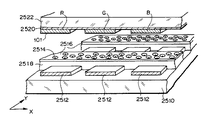
図25において、2510はガラスからなるリアプレート、2512はカソード配線(信号配線:Y方向)、2518は絶縁層、2516はゲート配線(走査配線:X方向)、2514はMoからなるエミッターチップであり、図37、38では簡略化して図示してあるが、ゲート配線とカソード配線の各交差部に約300個のエミッターチップが形成されている。各交差部のエミッタ群がフェースプレート上に形成された各色の蛍光体にそれぞれ対応している。101は導電性が付与された3原色の蛍光体(R、G、B)がそれぞれ載置されたアノード電極、2520は絶縁層、2522はガラスからなるフェースプレートである。本参考例では、図25に示すように、ゲート配線(走査配線:X方向)と分割されたアノード電極101の方向(Y方向)とが直交するようになっている。
【0251】
また、図37、38に示す様に、本参考例の画像形成装置では、X方向にプレート状のスペーサ2540を配置している。つまり、カソード配線2512間、及び分割されたアノード電極101間をまたがってスペーサ2540を配置している。
【0252】
本参考例で用いたスペーサ2540は図37、38に示す様に、放電を誘発する可能性のある鋭角な部分ができないよう角部を削って形状加工したガラス板の表面にポリイミドの膜をコートした絶縁性のスペーサを用いている。絶縁性スペーサのフェースプレートとリアプレート間方向の高さは1mmであり、X方向の長さは4mmとした。このスペーサを図38に示すように、ゲート配線間に配置し、画像形成装置内の全面にわたってジグザグ状に配置してある。
【0253】
本参考例の画像形成装置の製造方法を以下に記す。
【0254】
本参考例のフェースプレートには参考例1と同様にフォトリソグラフィー法を用いて、100μmピッチに分割されたITO電極上に3原色(Red、Green、Blue)の導電性の付与された蛍光体をそれぞれ形成した(101)。
【0255】
一方リアプレート側は、参考例6と同様にフォトリソグラフィー法を用いて、ゲート配線とカソード配線の各交差部に約300個のエミッタ−チップを形成した。尚、ゲート配線間ピッチを300μmとし、カソード配線間ピッチを100μmで形成した。
【0256】
次に、ゲート配線2516間に前述の絶縁性スペーサを不図示のフリットによりリアプレート側に固定し、さらに、絶縁性スペーサのフェースプレート側の固定部にもフリットを塗布・仮焼成(フリットに含まれる有機物を加熱除去)した。
【0257】
そして、スペーサを固定したリアプレートの外周部に、既に仮焼成したフリットが配置された枠部材(不図示)を載置した。
【0258】
次に、以上の様にした作成したフェースプレート上の分割されたアノード電極101と、リアプレート上のカソード配線2512とが平行になるように位置決めし、高真空中で、フェースプレートとリアプレート間間隔方向に加圧しながら加熱および冷却することで、フリットによる封着を行い、内部が高真空に維持された画像形成装置を作成した。
【0259】
この様にして作成した電界放出型電子放出素子を用いた画像形成装置に不図示の駆動回路を接続し、アノード電極に3kVの高電圧を印加し、電子放出素子を駆動したが、放電と見られる発光は確認されなかった。
【0260】
尚、本参考例では、絶縁性スペーサとして平板状のものを用いた例を示したが、アノード電極あるいはカソード配線間隔未満の直径を有する公知の棒(ファイバー)状の絶縁性スペーサを用い、カソード配線間及びアノード電極間をまたがらないようにスペーサを配置した画像形成装置でも放電と見られる発光及び電子放出素子の破壊等も確認されなかった。
【0261】
電子放出素子を設けた電子放出装置の構成例として、電子放出素子の電極や、電子放出素子への配線を電子放出素子が設けられた基板側の電極とし、該基板に対向する電極を分割する構成にした例を示した。本発明は、電圧を印加する様々な構成に適用可能である。また、例えば平板対向型の表示装置には好適に採用しうる。また、対向する電極間に印加される高電圧がDC電圧又はDCに近い(若干の変調による電圧変動を含む)電圧が印加される構成に対しても特に有効である。
【0262】
【発明の効果】
以上述べたように、本発明では、両極間での放電の影響を抑制することができる。より具体的に言えば、両極間の静電容量を実質的に小さくすることができる。
【0263】
より具体的には、電圧印加装置としては、放電の際の放電量を少なくすることができ、また電子放出装置としては、放電による電子放出素子への影響を緩和でき、良好な耐久性、長寿命化を実現できる。
【図面の簡単な説明】
【図1】 本発明の電子放出装置に用いるフェースプレートの一例を示す平面図である。
【図2】 図1、図5のフェースプレートに蛍光体を塗布した状態を示す平面図である。
【図3】 本発明の電子放出装置に用いるリアプレートの一例を示す平面図である。
【図4】 従来例(比較例)のフェースプレートを示す平面図である。
【図5】 図1のフェースプレートの変形例である。
【図6】 表面型電子放出素子以外の冷陰極アレーの例(リアプレートの一部)を示す断面図である。
【図7】 従来の電子放出装置の動作を説明するための等価回路図である。
【図8】 本発明の電子放出装置の動作を説明するための等価回路図である。
【図9】 従来の電子放出装置の動作を説明するための等価回路図である。
【図10】 本発明の電子放出装置の動作を説明するための等価回路図である。
【図11】 本発明のフェースプレートの別の例を示す図である。
【図12】 表面型電子放出素子の概念図である。
【図13】 表面伝導型放出素子の作製工程を示す図である。
【図14】 フォーミング工程での電圧印加の例を示す図である。
【図15】 Alメタルバックを具備した場合のフェースプレートの例を示す平面図である。
【図16】 図15のフェースプレートの別の例を示す平面図及び断面図である。
【図17】 本発明が適用される平面ディスプレイの典型例を示す図である。
【図18】 蛍光膜の構成を示す図である。
【図19】 電子放出装置を示す概念図である。
【図20】 本発明の参考例8におけるフェースプレートの平面図である。
【図21】 本発明の参考例9におけるフェースプレートの平面図である。
【図22】 本発明の参考例9におけるフェースプレートの断面図である。
【図23】 本発明の参考例10におけるフェースプレートの拡大図である。
【図24】 本発明の参考例10におけるフェースプレートの平面図である。
【図25】 本発明の参考例16における画像形成装置の概略構成図である。
【図26】 本発明の参考例10におけるフェースプレートの平面図である。
【図27】 本発明の参考例11におけるフェースプレートの平面図である。
【図28】 リアプレートの平面図である。
【図29】 本発明の画像形成装置の一例を示す概略構成図である。
【図30】 本発明の画像形成装置の一例を示す断面図である。
【図31】 本発明の実施例に係わる画像形成装置の構成図である。
【図32】 本発明の実施例に係わる画像形成装置の電子源の製法図である。
【図33】 本発明の実施例に係わるスペーサの製法図である。
【図34】 本発明の実施例、参考例13に係わるフェースプレートの構成図である。
【図35】 本発明の比較例に係わるスペーサの製法図である。
【図36】 本発明の参考例15に係わるスペーサの製法図である。
【図37】 本発明の参考例16の画像形成装置の断面図である。
【図38】 本発明の参考例16のリアプレートの平面図である。
【符号の説明】
1 電子源基板(リアプレート)
2 陽極基板(フェースプレート)
3 スペーサ
4 ガラス基板
5 電子放出素子
6a,6b 素子電極
7a 配線電極(走査電極)
7b 配線電極(信号電極)
8 基板
9 透明電極
10 蛍光体
11 帯電防止膜
12 接触電極
13 外枠
14 層間絶縁層
31 導電性薄膜
32 電子放出部[0001]
BACKGROUND OF THE INVENTION
The invention related to this application isElectronicThe present invention relates to an image forming apparatus that forms an image by the above.
[0002]
[Prior art]
Conventionally, as an application form of an electron emission device using an electron emission element, there is an image forming apparatus. For example, an electron source substrate on which a large number of cold cathode electron emission elements are formed, and electrons emitted from the electron emission element are accelerated. 2. Description of the Related Art A flat-type electron beam display panel is known in which a metal back or a transparent electrode and an anode substrate provided with a phosphor face each other in parallel and are evacuated to a vacuum. In such an image forming apparatus, a device using a field emission type electron-emitting device is described in, for example, Brodie, "Advanced technology: flat cold-cathode CRTs", Information Display, 1/89, 17 (1989). A device using a surface conduction electron-emitting device is disclosed in, for example, US Pat. No. 5,066,883. The flat-type electron beam display panel can achieve a lighter and larger screen than a cathode ray tube (CRT) display device that is widely used at present, and a flat-panel display using liquid crystal. Compared with other flat display panels such as panels, plasma displays, and electroluminescent displays, it is possible to provide images with higher brightness and higher quality.
[0003]
FIG. 17 shows a schematic configuration diagram of an electron beam display panel as an example of an image forming apparatus using electron-emitting devices. The configuration of this panel will be described in detail. In the figure, 31 is a rear plate which is an electron source substrate, 46 is a face plate which is an anode substrate, 42 is an outer frame, 41 is a glass substrate which is a base of the rear plate, These constitute a
[0004]
To form an image on this display panel,MatrixBy sequentially applying a predetermined voltage to the
[0005]
Although an example using a transparent electrode has been described here, a phosphor 45 is formed on a glass substrate 46, and a metal back made of aluminum or the like is further applied thereon to accelerate the electrons. It may also be used as an electrode for this purpose.
[0006]
FIG. 18 is a schematic view showing a fluorescent film. In the case of monochrome, the fluorescent film can be composed only of a phosphor. In the case of a color fluorescent film, it can be composed of a
[0007]
As a method of applying the phosphor on the glass substrate, a precipitation method, a printing method, or the like can be adopted regardless of monochrome or color. The purpose of using the metal back is to improve the brightness by specularly reflecting the light emitted from the phosphor toward the inner surface to the
[0008]
In order to further increase the conductivity of the fluorescent film 45, a transparent electrode (not shown) may be provided on the
[0009]
In the case of color, it is necessary to associate each color phosphor with the electron-emitting device, and sufficient alignment is required.
[0010]
Further, in the case of a flat type image forming apparatus using the electron beam as described above, when the display area is increased, the container is supported against the difference between the vacuum inside the container and the atmospheric pressure outside. A structural member may be required.
[0011]
When such a member is provided, a part of electrons emitted from the electron source near the spacer or reflected by the face plate collide with the spacer, or positive ions ionized by the emitted electron adhere to the spacer. As a result, the spacer may be charged. When the spacer is highly charged, the electrons emitted from the electron source are bent in their trajectories, reach a position different from the normal position on the phosphor, and when the display image is viewed from the entire surface, the image near the spacer is Displayed with distortion or contrast.
[0012]
In order to solve this problem, proposals have been made to remove the charge so that a minute current flows through the spacer (Japanese Patent Laid-Open Nos. 57-118355 and 61-124031). Therefore, charging is prevented by forming a high resistance film on the surface of the insulating spacer so that a minute current flows through the spacer.
[0013]
[Problems to be solved by the invention]
In the image forming apparatus of the type in which a high voltage is applied between the above-described positive electrode and the above-described metal back or transparent electrode for accelerating the cold cathode multi-electron source, in order to obtain the maximum emission luminance It is advantageous to apply a high voltage. Since the electron beam emitted depending on the type of element diverges before reaching the counter electrode, it is preferable that the distance between both electrodes is short in order to realize a high-resolution display.
[0014]
However, a phenomenon in which the
[0015]
In order to solve such a problem, it is necessary to reduce the frequency of discharge or to make it difficult to cause discharge breakdown.
[0016]
Causes of discharge destruction are that a large current flows into one point in a short time and the element is destroyed by heat generation, or that the voltage applied to the electron-emitting element rises momentarily to destroy the element. Conceivable.
[0017]
As a means for reducing the current causing the discharge breakdown, a method of inserting a limiting resistor in series as shown in FIG. 19 is conceivable. For example, vertical 500 elements × horizontal 1000 elements are driven line-sequentially by matrix wiring, When this method is adopted in this device in which about 1000 elements are turned on at the same time, the following new problem arises.
[0018]
Assuming that the emission current per element where about 1000 elements are turned on is 5 μA, an anode inflow current fluctuation of 0 to 5 mA is generated according to the image. Therefore, a series resistance of 1 MΩ is externally inserted into the anode. In the example of FIG. 19, when the voltage drop is 0 to 5 kV and acceleration is performed at a high voltage of 10 kV, luminance unevenness of about 50% at maximum occurs.
[0019]
Further, since a high voltage is applied to the opposing flat plates, the charge accumulated as a capacitor is, for example, the area of the cathode and anode in FIG.2The distance is 1 mm, and the potential difference between the anode and the cathode is 10 kV.-6Even if it reaches the coulomb and discharges at 1 μsec, the current of 1A concentrates in one place, which causes element destruction. Therefore, even if there is no brightness unevenness problem as described above, the addition of the external series resistance is sufficient solution It will not be.
[0020]
Therefore, an object of the present invention is to improve the configuration of voltage application.
[0021]
[Means for Solving the Problems]
An image forming apparatus according to the present invention is connected to an X direction wiring to which a scanning signal is applied, a Y direction wiring to which a modulation signal is applied, the X direction wiring and the Y direction wiring,By the scanning signal and the modulation signalA first substrate comprising a plurality of electron-emitting devices driven line-sequentially;
A second substrate comprising a plurality of electrodes connected to acceleration voltage applying means via a resistor and applied with a constant voltage;
It is arranged across two or more electrodes of the plurality of electrodes, maintains an interval between the first substrate and the second substrate, and is electrically connected to the wiring in the X direction and the two or more electrodes. An image forming apparatus having a support member connected to
The second substrate includes a plurality of phosphors positioned on each of the plurality of electrodes, and a plurality of phosphors positioned on each of the plurality of phosphors and at an interval equal to the interval between the plurality of electrodes. With a metal back,
Each of the plurality of electrodes and each of the plurality of metal backs has a shape extending in a direction non-parallel to the X direction,
The support member has a first member having a first conductivity, a second conductivity higher than the first conductivity, and the two or more electrodes and the first member. A plurality of second members electrically connected,
The plurality of second members are spaced apart from each other, and each of the second members is electrically connected to each of the two or more electrodes.
[0022]
Hereinafter, an electron emission device, an image forming device, and a voltage applying device related to the image forming device of the present invention will be described.
[0023]
The constant voltage referred to in the above invention is a voltage that does not involve switching between a voltage of a certain value and a voltage of another value during substantial operation, that is, a voltage that does not involve clear switching of ON and OFF. is there.
[0024]
Support memberSpecifically, the distance between the first substrate and the second substrate is prevented from changing due to the force due to the difference between the pressure between the first substrate and the second substrate and the pressure on the outside. Or the distance between the first substrate and the second substrate is kept substantially uniform.
[0025]
In the above invention, the support member may be capable of passing a current between the first substrate and the second substrate.Support memberWhen the charging of the support member becomes a problem due to the conductive property, the charging can be relaxed. Here, since the power consumption increases when the conductivity of the support member is improved (the current easily flows), it is preferable to set the conductivity in consideration of the power consumption and how much charging is desired to be eased. . In addition, when electrically connecting the support member having conductivity, a member having better conductivity may be provided at the connection portion so that the connection is good.
[0026]
The support memberHas a first member having first conductivity, and is configured to electrically connect the support member to the electrode, and to make a good electrical connection to a connection portion with the electrode. A second member for providing a good electrical connection when the second member having conductivity is provided and the support member is provided across at least two of the divided electrodes. Therefore, the divided electrodes are easily short-circuited. In order to suppress this, the second member having good second conductivity may be provided separately. At this time, the first conductivity may be set to such an extent that a short circuit between a plurality of divided electrodes can be suppressed within an allowable range. Of course, the first conductivity may be set so that a large current does not flow from the viewpoint of suppressing power consumption. Therefore, considering the suppression of the short circuit and the suppression of power consumption, It may be determined in consideration of the degree of mitigation.
[0027]
AlsoIn each invention using the first member having the first conductivity and the second member having the second conductivity, the member having the second conductivity is used in order to improve the electrical connection. The surface resistance of 10-1To 10-2Ω, and the surface resistance of the first conductive member is 108To 1011It is preferable to use Ω.
[0028]
In addition, the conductive support member in each of the above inventions can be variously configured. In particular, a conductive support member can be obtained by forming a film for imparting electrical conductivity to the surface of the substrate of the support member. By selecting the material, composition, thickness, and shape of the film, desired conductivity can be given.
[0029]
In each of the above-described inventions, an applied voltage may be set for each of the divided electrodes.
[0030]
AlsoIn the above invention, the resistance value of the resistor is preferably between 10 kΩ and 1 GΩ, or between 10 kΩ and 4 MG.
[0031]
In each of the above inventions, a plurality of the electron-emitting devices are provided, the resistance value of the resistor is R, the emission current value of each electron-emitting device is Ie, and the acceleration voltage applied by the electrode is V, divided. When the number of electron-emitting devices that emit electrons toward one electrode is n,
R ≦ 0.004 × V / (n × Ie)
It is preferable to satisfy the above condition.
[0032]
In each of the above inventions, the electron-emitting device is preferably a surface conduction electron-emitting device.
[0033]
hereThe image forming member may be a light emitter that emits light when irradiated with electrons, or may be a phosphor that emits light when irradiated with electrons.
[0034]
Here, the image forming member may be provided on a substrate on which the divided electrodes are provided.
[0035]
The divided electrodes may include electrodes having a horizontal to vertical ratio of 4: 3. Alternatively, the divided electrodes may have an overall horizontal to vertical ratio of 16: 9.There is.
[0036]
DETAILED DESCRIPTION OF THE INVENTION
Embodiments of the invention will be described below.
[0037]
At first,Electron emission deviceThe outline of the configuration will be described and compared with the conventionally known configuration using an equivalent circuit diagram.
[0038]
FIG. 7 shows an equivalent circuit of a conventional electron emission device. The rear plate substrate side on which a plurality of electron emission elements and a matrix wiring for selectively driving the elements are formed is at a potential almost close to GND. As a trigger, the discharge current Ib1 caused by the capacitor formed by the face plate and the rear plate fluctuates the element applied potential. The degree of variation depends on the circuit configuration on the rear plate side (simulated by resistance Rr), but in the case of a surface conduction electron-emitting device, the device deteriorates even when the device driving voltage is typically about 1 to 5 Volt. There is.
[0039]
In the present invention, as shown in FIG. 8, the face plate side electrodes (transparent electrode 44 in FIG. 17 and the above-described metal back, etc.) are divided and a high resistance R1 is inserted into each of them to reduce the capacitor capacity and reduce the discharge current Ib2. Reduced. As a result, voltage fluctuations applied to the device due to the discharge current are reduced, and damage during discharge is improved. In FIG. 8, each electrode is connected in parallel through a resistor. Here, if a large number of electron-emitting devices are arranged so as to be selected on the cathode side, an electron-emitting type or other electron-emitting devices can be preferably used.
[0040]
A structure having a plurality of divided anodes is disclosed in U.S. Pat. No. 5,225,820, which splits the anodes in order to select (address) phosphors to emit light. It does not include all the components.
[0041]
FIGS. 9 and 10 show the portion corresponding to the resistor Rr in FIGS. 7 and 8 in more detail, and a switch for inputting an image signal is connected through the resistor Rs of each element. It is considered that the breakdown due to the discharge occurs when the voltage across the Rs becomes too large.
[0042]
As described above, according to the present invention, the charge accumulated in the capacitor component is reduced by dividing the anode (anode) into the anode. If divided into N, the amount of accumulated charge becomes 1 / N. In addition, by making the electrode separation non-parallel to the direction in which elements that can be driven at the same time are arranged, the range of current that can simultaneously flow into each of the divided electrodes is narrowed, and the voltage drop can be suppressed. . Further, in particular, by making the direction in which the simultaneously driven elements are arranged orthogonal to the direction of division, the maximum value of the emission current flowing into each electrode is reduced to 1 / N, so the voltage drop is also reduced to 1 / N. I can do it. Therefore, the luminance unevenness caused by the additional resistance and the charge accumulated as the capacitor can be reduced at the same time. That is, the discharge damage is effectively reduced without adverse visual effects.
[0043]
Further, the divided areas of the anodes are not necessarily equal, and may be divided so that the areas of the anodes are different as shown in FIG.
[0044]
In general, the larger N is, the greater the effect is. However, even when N = 2, the accumulated charge can be halved, and the maximum emission current flowing in can be reduced to ½ by arranging a current limiting resistor for each anode. There is. The maximum value of N is determined by the production accuracy limit. However, when one pixel is opposed to the electrode, the luminance distribution due to the voltage drop is suitably suppressed. Therefore, N is arranged in a matrix of m × 1 pixels. In this case, it is preferable to separate each pixel with N = m × l. It is easy to separate up to about the number of elements that are driven simultaneously in normal line order, and the effect can be expected sufficiently.
[0045]
For example, when 1000 elements are driven simultaneously as shown in FIG. 1, the ITO electrode, which is the anode of the face plate, is divided into 1-1000 as shown in FIG. FIG. 3: For example, alignment is performed so as to correspond to 1 to 1000 emission points on the v004 common electrode (scanning electrode), and the panel is sealed as shown in FIG.
[0046]
The
[0047]
However, in the case where an electrode that is not at the end is generated when the rectangular face plate is separated into an m × 1 matrix, a configuration in which wiring to the electrode that is not at the end is provided in the pattern can be taken. When realizing the present invention without making an isolated electrode that requires such wiring, it is easy to make a resistance to connect and an extraction electrode by setting either m or l to 2 or less.
[0048]
The number of divisions of the anode of the face plate is not provided corresponding to the number of element arrangements of the rear plate, and the anode is divided and formed for each block of emission points of
[0049]
The anode division is arranged so as to be orthogonal to the element arrangement and there is no division break in the pixel, but the design is easier, but the effect is not lost even if it is crossed obliquely as shown in FIG.
[0050]
Here, when an appropriate resistance value in the example of 1000 element simultaneous line sequential driving is estimated, 0.1 to 1000 MΩ is preferable when the emission current of 1 element is 1 to 10 μA. The practical upper limit of the resistance value is determined in a range where luminance drop does not occur when the voltage drop is about 1 to several tens of Va or less.
[0051]
In general, when a metal back treatment with a thickness of about 1000 angstroms to 2000 angstroms is performed on a phosphor, the accelerated electron transmittance is about 10 kV and the transmittance is close to 1. High efficiency. If the voltage drop of 1 kV at an acceleration voltage of 10 kV is taken as one guide when designed to accelerate at 10 kV, there are examples of combinations such as <10 μA, 100 MΩ, 1 μA, 1000 MΩ> depending on the emission current value. The lower limit of the resistance value can be selected to such an extent that the current flowing in a DC manner does not hinder device destruction. At 0.1 MΩ and Va = 10 kV, a current of 100 mA flows, and this is a region where the breakdown becomes remarkable. However, the breakdown depends on the characteristics of the electron-emitting device, the wiring resistance value, and the switching resistance value of the scanning electrode / signal electrode. Therefore, the resistance value to be added is specifically selected from 0.01 MΩ to 10 GΩ. It is considered that 1 MΩ to 100 MΩ functions more effectively.
[0052]
In addition, for example, 256 gray scales are a specification for high-quality demands such as TV receivers, so it is important to suppress luminance unevenness below that level.
[0053]
In order to suppress the 256 gradations, that is, the width of 0.4%, it is necessary to make the fluctuation range of the voltage of the anode within about 0.4%. Therefore, the voltage drop due to the resistance should be limited to the width.
[0054]
In other words, when connecting resistors to the divided anodes and driving with common wiring, it is desirable that the voltages in the region where electrons are actually accelerated are accurately aligned. The adjusted electrodes are adjusted so that the respective voltages are aligned.
[0055]
Assuming that the luminance is linear with respect to the accelerating voltage, if the number of elements that are turned on simultaneously among the divided anodes to which the accelerating voltage V is applied is n, the allowable voltage drop amount is ΔV. Since ΔV / V should be 0.004, the resistance connected to the anode is R, and the emission current value flowing from one element is Ie
Since ΔV = R × n × Ie
R = 0.004 × V / (n × Ie)
Since the minimum value of lighting number n is 2,
R ≦ 0.002 × V / Ie.
When Va = 10 kVolt and Ie = 5 μA, R ≦ 4 MΩ.
Similarly, if n is 3, then R ≦ 2.67 MΩ.
[0056]
When an element is driven using simple matrix wiring to display an image, line sequential scanning is generally performed. As a preferred application method of the present invention in the case of performing line sequential scanning, the accelerating electrode division pattern is arranged perpendicular to one line of scanning wiring selected simultaneously during scanning. Therefore, the influence of the voltage drop due to the resistance connected to the divided acceleration electrode on the luminance distribution is a result of dividing the number of electron-emitting devices connected to one scanning wiring by the number of divisions dividing one scanning wiring horizontally. Since n in the above equation is determined, a larger resistor R can be connected when the number of divisions is determined.
[0057]
Furthermore, in view of the case where a means such as laser trimming is necessary to achieve 0.4% accuracy in the production of a general thin film resistor, which leads to a long process time and a factor of cost increase, the present invention is divided. This problem is solved by providing a setting means that can vary the driving conditions for each element facing the divided electrodes in order to correct the luminance variation due to the accuracy of the resistance connected to the acceleration electrode.
[0058]
The antistatic film on the spacer is for removing charges accumulated on the surface of the insulating substrate by coating the surface of the insulating substrate with a conductive film. Usually, the surface resistance of the antistatic film is 10%.12It should be Ω or less. Furthermore, in order to obtain a sufficient antistatic effect, a lower resistance value may be used.11The resistance is preferably Ω or less, and if the resistance is lower, the charge removal effect is improved.
[0059]
When the antistatic film is applied to the spacer of the image forming apparatus, the surface resistance of the spacer is set in a desirable range from the antistatic and power consumption. The lower limit of the surface resistance is limited by the power consumption in the spacer. The lower the resistance, the quicker the charge accumulated in the spacer can be removed, but the power consumed by the spacer increases. The antistatic film used for the spacer is preferably a semiconductive material rather than a metal film having a small specific resistance. The reason is that when a material having a small specific resistance is used, the antistatic film must be made very thin in order to obtain a desired surface resistance. Although it depends on the surface energy of the thin film material, the adhesion to the substrate and the substrate temperature, it is generally 102Thin films below angstroms are island-shaped, unstable resistance, and poor film reproducibility.
[0060]
Therefore, a semiconductive material having a specific resistance value larger than that of the metal conductor and smaller than that of the insulator is preferable. However, many of these materials have a negative resistance temperature coefficient. If the temperature coefficient of resistance is negative, the resistance value decreases due to the temperature rise due to the electric power consumed on the spacer surface, further generates heat, and the temperature continues to rise, causing so-called thermal runaway in which excessive current flows. However, thermal runaway does not occur in a situation where the heat generation amount, that is, power consumption and heat dissipation are balanced. Also, if the absolute value of the resistance temperature coefficient TCR of the antistatic film material is small, thermal runaway is difficult.
[0061]
Spacer 1cm under the condition using antistatic film with TCR -1%2Experiments have confirmed that when the power consumption per unit exceeds about 0.1 W, the current flowing through the spacer continues to increase, resulting in a thermal runaway state. Of course, depending on the spacer shape, the voltage Va applied between the spacers and the resistance temperature coefficient of the antistatic film, the power consumption is 1 cm from the above conditions.2The value of the surface resistance not exceeding 0.1 W per unit is 10 × Va2Ω or more. That is, the surface resistance of the antistatic film formed on the spacer is 10 × Va.2Ω to 1011It is preferable to set in the range of Ω.
[0062]
As described above, the antistatic film formed on the insulating substrate has a film thickness of 102Angstrom or more is desirable. On the other hand, the film thickness is 10FourAbove angstroms, the film stress increases and the risk of film peeling increases, and the film formation time becomes longer, resulting in poor productivity. Therefore, the film thickness is 102-10FourAngstrom, or 2.0 × 10²~ 5.0 × 10ThreeAn angstrom is desirable. The specific resistance is the product of the surface resistance and the film thickness. From the preferred range described above, the specific resistance of the antistatic film is 10-Five× Va2-107It is good that it is Ωcm. Furthermore, in order to realize a more preferable range of surface resistance and film thickness, 2.0 × 10-Five× Va2~ 5.0 × 10⁶It is good to use Ωcm.
[0063]
The acceleration voltage Va of electrons in the image forming apparatus is 100 or more, and a voltage of 1 kV is required to obtain sufficient luminance. Under the condition of Va = 1 kV, the specific resistance of the antistatic film is 10-10.7Ωcm is a preferred range.
[0064]
Further, in order to obtain good electrical contact with the anode electrode and the wiring electrode, a strip-shaped contact electrode is preferably formed on the spacer with a metal conductive film. That is, an antistatic film is provided as the first member having the first conductivity, and the second electrode having the second conductivity is provided to improve the electrical connection between the antistatic film and the anode electrode or the wiring electrode. A contact electrode (metal conductive film) may be provided as the member.
[0065]
Therefore, in the present invention, a spacer may be arranged so as not to straddle the divided anode electrode so that the divided anode electrode is not electrically short-circuited.
[0066]
In the present invention, the contact electrode may be formed without electrically short-circuiting the divided anode electrode with respect to the spacer arranged over the divided anode electrode.
[0067]
For example, the surface resistance is 10-1-10-2The contact electrode set to Ω is formed in an island shape on the divided anode electrode side. The surface resistance of the antistatic film is 108To 1011It is set to Ω and prevents an electrical short circuit between island-shaped contact electrodes and between divided anode electrodes. Furthermore, when the width of the island-shaped contact electrode is smaller than the distance between the divided anodes, alignment at the time of assembling the spacer is simple or unnecessary, and the spacer can be assembled by a simple method using a conventional figure hole jig. . Moreover, when the pitch of the island-shaped contact electrodes is formed smaller than the spacer height, the influence on the emitted electron trajectory can be suppressed, and a desirable effect can be expected.
[0068]
An image forming apparatus using a face plate in which a plurality of divided anode electrodes commonly connected to a spacer having the above-described configuration through a current limiting resistor are disposed, and a light emitting portion that emits light by irradiation with an electron beam is formed. By applying to the above, it is possible to obtain a display image with high brightness and no distortion, and further, it is possible to manufacture a long-life image forming apparatus without element destruction.
[0069]
29 and 30 are schematic views showing an example of the configuration of the image forming apparatus using the spacer of the present invention, and FIG. 30 is a cross-sectional view taken along line AA ′ in FIG.
[0070]
29, 1 is a rear plate which is an electron source substrate, 2 is a face plate which is an anode substrate, 3 is a spacer, 4 is a substrate which is a base of the
[0071]
The
[0072]
FIG. 31 is a configuration diagram of an image forming apparatus according to this configuration example, and FIG. 32 is a manufacturing diagram of an electron source of the image forming apparatus according to this configuration example. 31 and 32, the same parts as those shown in FIGS. 29 and 30 are denoted by the same reference numerals as those shown in FIGS. In FIG. 32, 31 is a conductive thin film, and 32 is an electron emission portion. For the conductive
[0073]
As the
[0074]
Various arrangements of the electron-emitting devices 5 can be employed. What is described here is an arrangement called a simple matrix arrangement, in which a plurality of electron-emitting devices 5 are arranged in a matrix in the X and Y directions, and a plurality of electron-emitting devices 5 arranged in the same row are arranged. One electrode 6a is commonly connected to the X-direction wiring 7a, and the
[0075]
In the above configuration, individual elements can be selected and driven independently by simple matrix driving.
[0076]
In addition, a plurality of electron-emitting devices arranged in parallel are connected at both ends, and a plurality of rows of electron-emitting devices are arranged (referred to as a row direction), and a direction perpendicular to the wiring (referred to as a column direction). There are ladder-type arrangements in which electrons from the electron-emitting devices are controlled and driven by a control electrode (also referred to as a grid) disposed above the electron-emitting devices, but the present invention is particularly limited by these arrangements. It is not something.
[0077]
The
[0078]
The metal back 9 is divided and patterned by photolithography so as to be arranged parallel to the Y-direction wiring 7b and perpendicular to the X-direction wiring 7a in order to keep the voltage drop as small as possible, and further, a current limiting resistance of about 100 MΩ for each divided column A positive high voltage Va is applied from an external power source (not shown) to the extraction portion commonly connected via the. At this time, the width La and the pitch Pa of the divided anode electrodes differ depending on the number of elements in the image forming apparatus, the element pitch Px on the X-direction wiring side, etc., but are generally defined as follows.
[0079]
Pa = n · Px (n∈N | n <100)
10-6m ≦ Pa−La ≦ 10-Fourm
Thus, the electrons emitted from the electron-emitting device 5 are attracted to the
[0080]
In FIG. 31, the outer frame 13 is connected to the
[0081]
Hereinafter, an example of a manufacturing method of the spacer of the present invention will be described.
[0082]
First, a contact electrode is formed of a conductive metal on a cleaned glass substrate by a vacuum deposition method, a sputtering method, a printing method, a pulling method, or the like. With respect to the scale of the island-like contact electrode on the face plate side, it is desirable to satisfy the following conditions using the reference numerals in FIG.
[0083]
First, the condition that the island-shaped contact electrode does not short-circuit a plurality of divided anode lines by any alignment,
Lc <Pa -La ...(1)
Second, the condition for suppressing the electric field unevenness that causes the bright spot variation between elements due to the island-shaped contact electrode,
Pc ≤ Px ≤ Pa ...(2)
H << d ...(3)
Regarding the scale of the strip-shaped contact electrode on the rear plate side, it is desirable to satisfy the second condition.
[0084]
H '<< d ...(4)
The spacer on which the contact electrode is formed in this manner is further formed with an antistatic film having conductivity by a vacuum deposition method, a sputtering method, a printing method, a pulling method or the like.
[0085]
The surface resistance Rs of this antistatic film is
108Ω <Rs <1011Ω
Desirably set in a range. The lower limit of the resistance is defined from suppression of a short circuit between the divided anode electrodes, suppression of power consumption, and the like, and the upper limit is defined in a range where the antistatic effect of the spacer is recognized.
[0086]
If the above conditions are satisfied, a uniform image forming apparatus can be produced without the positional alignment of the spacer and the face plate, and without any positional variation in discharge tolerance and emission electron trajectory.
[0087]
【Example】
Hereinafter, the present invention will be described in more detail with reference to examples.In order to facilitate understanding of the present invention, reference examples will also be described.
[0088]
ExampleAnd reference examplesSuppose that the scanning wiring has parallel to the X direction and the signal wiring has parallel to the Y direction with respect to the XY axis.
[0089]
[Reference example1]
An image forming apparatus using the electron-emitting device described in FIG. As shown in FIG. 3, the multi-electron source of the rear plate isMatrixWired SEC electron source (to be described in detail later).
[0090]
On the other hand, as shown in FIG. 1, the face plate is formed with a solid ITO film on a glass substrate, and then separated (101) by a photolithography process at a pitch of 230 μm (1000 lines), and one side has a 100 MΩ resistor ( A high voltage can be applied from the terminal 103 by bundling through the patterned NiO film (102).
[0091]
Next, as shown in FIG. 2, phosphor ZnS (Cu dope) is applied and fired on the separated ITO, 201 and 202, and a face plate for applying an anode high voltage to the cold cathode multi-electron source (rear plate) is obtained. .
[0092]
The common wirings v001, v002,... On the rear plate and the
[0093]
The gap between the face plate of FIG. 1 and the rear plate of FIG. 3 was 2 mm, and a high voltage Va: 5 kV was applied. Line-sequential driving was scrolled at 30 μsec per line at the TV rate. In order to investigate the influence of the discharge between the rear plate and the face plate, the measurement was performed by reducing (decreasing) the degree of vacuum in the image forming apparatus. Discharge was observed about twice per hour by measuring the external circuit and detecting the bright spot of the phosphor with a CCD, but no significant deterioration in luminance of the pixel was observed. For comparison, when the ITO of the prototype face plate was not separated (FIG. 4), significant luminance degradation of the pixels was observed along the vertical and horizontal wirings.
[0094]
In FIG. 4, 401 indicates an ITO film, and 403 indicates an extraction electrode.
[0095]
Hereinafter, the surface conduction type (SCE) electron-emitting device used in the present invention will be described. 12A and 12B are schematic views showing the configuration of a planar surface conduction electron-emitting device to which the present invention can be applied. FIG. 12A is a plan view and FIG. 12B is a cross-sectional view. In FIG. 12, 311 is a substrate, 312 and 313 are device electrodes, 314 is a conductive thin film, and 315 is an electron emission portion.
[0096]
The
[0097]
The element electrode interval SL, the element electrode length SW, the shape of the conductive
[0098]
The element electrode length SW can be in the range of several micrometers to several hundred micrometers in consideration of the resistance value of the electrode and the electron emission characteristics. The film thickness d of the
[0099]
The conductive
[0100]
The material forming the conductive
[0101]
The fine particle film described here is a film in which a plurality of fine particles are aggregated, and the fine structure thereof is a state in which the fine particles are individually dispersed and arranged, or a state in which the fine particles are adjacent to each other or overlap each other (some fine particles are aggregated, Including the case where an island-like structure is formed as a whole). The particle size of the fine particles is in the range of several angstroms to several thousand angstroms, preferably in the range of 10 angstroms to 200 angstroms. In the present specification, the term “fine particles” is frequently used, and the meaning thereof will be described.
[0102]
Small particles are called “fine particles”, and smaller particles are called “ultrafine particles”. It is widely used to call a “cluster” that is smaller than “ultrafine particles” and has about several hundred atoms or less.
[0103]
However, each boundary is not strict and changes depending on what kind of property is focused on. In addition, “fine particles” and “ultra fine particles” may be collectively referred to as “fine particles”, and the description in the present specification follows this. "Experimental physics course 14: Surface and fine particles" (Kinoshita Yoshio, Kyoritsu Shuppan, published September 1, 1986) describes as follows.
[0104]
“In this paper, the term“ fine particle ”means that the diameter is about from 2 to 3 μm to about 10 nm, and particularly the term“ ultrafine particle ”means that the particle size is about 10 nm to about 2 to 3 nm. It's just a rough guide because it is simply written as a fine particle, and it is called a cluster when the number of atoms constituting the particle is from 2 to several tens to several hundreds. ”(Page 195) 22nd to 26th lines)
In addition, the definition of “ultrafine particles” in the “forest / ultrafine particle project” of the New Technology Development Corporation was as follows. “In the“ Ultra Fine Particle Project ”(1981-1986) of the Creative Science and Technology Promotion System, those whose particle size (diameter) is in the range of approximately 1 to 100 nm are called“ ultra fine particles ”. Then, one ultrafine particle is about 100 to 108It is an aggregate of about one atom. From the atomic scale, ultrafine particles are large to huge particles. "
("Ultra-fine particle creation science and technology" Hayashi Lord Tax, Ryoji Ueda, Akira Tazaki edited by Mita Publishing, 1988,
Based on the general term as described above, in this specification, “fine particles” are an aggregate of a large number of atoms / molecules, the lower limit of the particle size is about several angstroms to 10 angstroms, and the upper limit is about several μm. I will refer to things.
[0105]
The
[0106]
There are various methods for manufacturing the surface conduction electron-emitting device described above, and an example is schematically shown in FIG.
[0107]
Hereinafter, an example of the manufacturing method will be described with reference to FIG. Also in FIG. 13, the same reference numerals as those in FIG. 12 are attached to the same parts as those shown in FIG.
[0108]
1) The
[0109]
2) An organometallic solution is applied to the
[0110]
3) Next, a forming process is performed. A method using energization processing will be described as an example of the forming process. When energization is performed between the
[0111]
The voltage waveform is preferably a pulse waveform. For this purpose, the method shown in FIG. 14 (a) in which a pulse having a pulse peak value as a constant voltage is continuously applied and the method shown in FIG. 14 (b) in which a voltage pulse is applied while increasing the pulse peak value. There is.
[0112]
T1 and T2 in FIG. 14A are the pulse width and pulse interval of the voltage waveform. Usually, T1 is set in the range of 1 microsecond to 10 milliseconds, and T2 is set in the range of 10 microseconds to 100 milliseconds. The peak value of the triangular wave (peak voltage during energization forming) is appropriately selected according to the form of the surface conduction electron-emitting device. Under such conditions, for example, a voltage is applied for several seconds to several tens of minutes. The pulse waveform is not limited to a triangular wave, and a desired waveform such as a rectangular wave can be adopted.
[0113]
T1 and T2 in FIG. 14B can be the same as those shown in FIG. The peak value of the triangular wave (peak voltage during energization forming) can be increased, for example, by about 0.1 V step.
[0114]
The end of the energization forming process can be detected by applying a voltage that does not cause local destruction or deformation of the conductive
[0115]
4) It is preferable to perform a process called an activation process on the element after forming. The activation process is a process in which the device current If and the emission current Ie are remarkably changed by this process.
[0116]
The activation step can be performed, for example, by repeating the application of pulses in the same manner as the energization forming in an atmosphere containing an organic substance gas. This atmosphere can be formed by using the organic gas remaining in the atmosphere when the inside of the vacuum vessel is evacuated using, for example, an oil diffusion pump or a rotary pump. It can also be obtained by introducing a gas of an appropriate organic substance in a vacuum. The preferable gas pressure of the organic substance at this time is appropriately set according to the case because it varies depending on the application form, the shape of the vacuum container, the kind of the organic substance, and the like. Examples of suitable organic substances include alkanes, alkenes, alkyne aliphatic hydrocarbons, aromatic hydrocarbons, alcohols, aldehydes, ketones, amines, organic acids such as phenol, carvone, and sulfonic acid. Specifically, methane, ethane, propane, etc. CnH2n + 2Saturated hydrocarbon, ethylene, propylene, etc. represented by CnH2nAn unsaturated hydrocarbon represented by a composition formula such as benzene, toluene, methanol, ethanol, formaldehyde, acetaldehyde, ascent, methyl ethyl ketone, methylamine, ethylamine, phenol, formic acid, acetic acid, propionic acid and the like can be used. By this treatment, carbon or a carbon compound is deposited on the element from an organic substance present in the atmosphere, and the element current If and the emission current Ie are remarkably changed. The end determination of the activation process is appropriately performed while measuring the device current If and the emission current Ie. The pulse width, pulse interval, pulse peak value, etc. are set as appropriate.
[0117]
Carbon and carbon compounds include, for example, graphite (so-called HOPG, PG, and GC. HOPG is an almost perfect crystal structure of graphite, PG is a crystal grain having a crystal structure of about 200 angstroms, and the crystal structure is slightly disordered, and GC is a crystal. This refers to those in which the grain size is about 20 angstroms and the disorder of the crystal structure is further increased.), Amorphous carbon (refers to amorphous carbon and a mixture of amorphous carbon and graphite microcrystals), and its film thickness Is preferably in the range of 500 angstroms or less, and more preferably in the range of 300 angstroms or less.
[0118]
5) The electron-emitting device obtained through such steps is preferably subjected to a stabilization step. This step is a step of exhausting the organic substance in the vacuum vessel. The pressure in the vacuum vessel is 1 to 3 × 10⁻⁷Torr or less is preferable, and further 1 × 10⁻⁸Torr or less is particularly preferable. As the vacuum exhaust device for exhausting the vacuum vessel, it is preferable to use a device that does not use oil so that the oil generated from the device does not affect the characteristics of the element. Specifically, vacuum exhaust apparatuses such as a sorption pump and an ion pump can be used. Further, when evacuating the inside of the vacuum vessel, it is preferable that the whole vacuum vessel is heated so that organic substance molecules adsorbed on the inner wall of the vacuum vessel or the electron-emitting device can be easily evacuated. The heating conditions at this time are preferably 80 to 200 ° C. for 5 hours or longer. However, the heating conditions are not particularly limited to these conditions. The heating conditions are appropriately selected according to various conditions such as the size and shape of the vacuum vessel and the configuration of the electron-emitting device. Do.
[0119]
The driving atmosphere after the stabilization process is preferably maintained at the end of the stabilization process, but is not limited to this, and the degree of vacuum itself is sufficient if the organic material is sufficiently removed. Can maintain sufficiently stable characteristics even if it drops somewhat. By adopting such a vacuum atmosphere, deposition of new carbon or a carbon compound can be suppressed, and as a result, the device current If and the emission current Ie are stabilized.
[0120]
[Reference example2]
BookReference exampleThen, as shown in FIG. 15, conductive black stripes; BS (60% carbon and 40% water glass component dispersed) were screen-printed on a faceplate glass substrate (1001). The width was 100 μm, the pitch was 230 μm, and the thickness was 10 μm. The resistance value is 150Ω / □.
[0121]
RuO as a high resistance body2Printed. The resistance value was 10 MΩ at a width of 100 μm and a length of 750 μm (1002). Next, the phosphor P22 for CRT was applied in a stripe shape between the BS, R, G, and B at a thickness of 10 μm and baked. Subsequently, an Al metal back was applied (1003). After forming an acrylic resin by dipping, 1000 Å of Al is deposited and fired. The target face plate was obtained by separating the Al film from the Al side by laser processing.
[0122]
This elementReference exampleWith one rear plateReference example1 was sealed, a panel was formed, and the same discharge resistance test was conducted. Discharge was observed about 2 to 5 times / hour, but no significant deterioration in luminance of the pixel was observed, and the Al film was separated. The effect of remarkably reducing the discharge damage was recognized as compared with the case of not. In addition, when the test was performed by changing the separation width every 1 line, 10 lines, and 100 lines as a test, it was found that the smaller separation width was more effective with less discharge damage. (FIG. 15 is a schematic view of this laser processing.IndicationIt is a thing. )
Specifically, in the 1-line and 10-line separation regions, there was no significant luminance degradation of the pixels, but in the 100-line portion, degradation over several pixels was observed (decrease in luminance).
[0123]
In a panel that does not separate Al as a comparative exampleReference exampleThe luminance degradation of the pixel occurred along the same wiring as in FIG.
[0124]
[Reference example3]
BookReference exampleThen, as shown in FIGS. 16 (a) and 16 (b),Reference exampleIn FIG. 16, in which Al oblique deposition was performed after the resin dipping performed in
[0125]
The height of the
[0126]
[Reference example4]
BookReference exampleThen, a conductive black stripe; BS (60% carbon, 40% water glass component dispersed) was screen-printed on a glass substrate constituting the face plate. BookReference exampleThen, the conductive black stripe also serves as the anode electrode. The width was 100 μm, the pitch was 230 μm, and the thickness was 10 μm. The resistance value is 150Ω / □. RuO as high resistance2Printed. The resistance value was 10 MΩ with a width of 100 μm and a length of 750 μm. Next, GREEN phosphor (ZnS, Cu doped In)2OThreeAddition, specific resistance of 109Ωcm) was formed on the entire surface of the display portion with a thickness of 10 μm. The resistance value between the conductive BSs is RuO2The resistance value is 10 MΩ, and the conductive phosphor resistance between adjacent BSs is separated by a parallel resistance of 300 MΩ.Reference exampleThe image forming apparatus was formed in the same manner as in No. 1, and the deterioration characteristics due to discharge were compared.Reference exampleThe same effective results were obtained as in the case of element isolation with the ITO pattern of 1. When ZnS not subjected to low resistance treatment is used, 1012Although it had a specific resistance of Ωcm and a slight charge-up phenomenon was observed, the effect of discharge resistance was recognized. As described above, it was proved that the present invention is effective if separation of about 1 to 100 MΩ can be performed on the faceplate anode.
[0127]
[Reference example5]
BookReference exampleThen, a transparent conductive film is formed on a glass substrate constituting the face plate, and Sb is doped so that the sheet resistance value becomes 100 KΩ / □.2OThreeFormed with.
[0128]
Reference examplePattern in stripes as in 1,Reference exampleAfter the resistance per one divided anode was set to 100 MΩ as in the case of No. 1, an Ag printed
[0129]
Reference exampleIn the same sealing process as No. 1, a panel was formed facing the rear plate to form a display. The resistance against discharge was superior to the comparative solid low resistance ITO sample shown in FIG. 4, and the luminance unevenness due to the voltage drop was also practical enough. The simultaneous emission current during the line-sequential driving experiment was ΣIe = 0 to 1 mA, and the luminance unevenness due to the voltage drop of the DC applied voltage was in an acceptable range.
[0130]
[Reference example6]
BookReference exampleThen, a field emission type electron-emitting device (FE) was used as the electron-emitting device.
[0131]
As shown in FIG. 6, a cathode film 706, an amorphous
[0132]
A 1000 × 500 cathode-side electron emission source was used as a rear plate with ˜2,000 electron-emitting devices as one pixel. The anode side is [Reference exampleUsing the face plate coated with the phosphor by the method of 1], it was sealed with the rear plate to form a display panel.
[0133]
A flat display was realized by applying a 600 V voltage between the face plate and the rear plate, and selectively driving the necessary pixels with the cathode electrode and the gate electrode on the rear plate. The panel using the face plate that did not divide the anode ITO (FIG. 4) was noticeably deteriorated due to the discharge at the tip of the gate electrode and the Mo cathode, but the ITO divided face plate (FIG. 1) was used. In those cases, the deterioration of discharge was remarkably reduced, and the effectiveness of the present invention was proved. That is, when ITO was divided, there was no significant deterioration in pixel luminance due to discharge during driving for a certain period of time. In the comparative example, 20 pixels having a luminance of 50% or less due to discharge were observed.
[0134]
[Reference example7]
BookReference exampleThe face plate structure will be described.Reference exampleIn the same way as in No. 1, an ITO film is formed on a glass substrate, separated into 230 μm pitches (1500 lines), and one side is a 100 MΩ resistor (RuO by screen printing)2The high voltage can be applied by bundling through separation formation (FIG. 1).
[0135]
Next, an insulating black stripe was printed for each separation groove on the separated ITO, and then each color RGB phosphor (P22) was periodically applied and fired on the separated
[0136]
The rear plate forms a 1500 × 500 SCE electron emission element, and the common wiring shown in FIG. 3 and the ITO separation wiring of the face plate are orthogonal (intersect) so that the electron emission element and the RGB phosphor face each other. Alignment sealed.
[0137]
The distance between the face plate and the rear plate was 3 mm, and a high voltage Va; 8 kV was applied. Line-sequential driving was scrolled at 30 μsec per line at the TV rate. The discharge between the rear plate and the face plate was measured by measuring the external circuit and detecting the bright spot of the phosphor with a CCD, and was observed about 5 times / hour at the beginning of the drive, but element degradation on the rear plate side was recognized. I couldn't. That is, no significant deterioration in the luminance of the pixels was observed. For comparison, when the ITO of the prototype face plate was not separated, there was a case where a significant deterioration of the luminance of the pixel due to the discharge was recognized along the horizontal and vertical wirings.
[0138]
[Reference example8]
BookReference exampleThe face plate structure in will be described.
[0139]
As shown in FIG. 20, three Ag extraction wirings 103 were printed on the face plate glass substrate. Vertical and horizontal insulating black stripes were screen printed. The width was 100 μm, the horizontal pitch was 282 μm, the vertical width was 300 μm, the vertical pitch was 842 μm, and the thickness was 10 μm. The take-out wiring is connected to the power sources V1, V2, and V3 through three external resistors so that an acceleration voltage can be applied. The respective resistance values were 10.1 MΩ, 10.3 MΩ, and 10.4 MΩ.
[0140]
Next, the phosphor P22 for CRT was coated with R, G, and B in a stripe shape between BSs in a thickness of 15 μm and baked. Subsequently, an Al metal back was formed. (After forming the acrylic resin by dipping, 1000 Å of Al is deposited and baked.) The face plate has a display area of about 16: 9.
[0141]
The target face plate was obtained by separating the Al film from the two Al sides along the 320th vertical black stripe from the left and right by laser processing. The rear plate formed a 2556 × 480 SCE electron-emitting device.
[0142]
The face plate and the rear plate were aligned and sealed so that the electron-emitting device and the RGB phosphor face each other. The gap between the face plate and the rear plate was 3 mm, and a high voltage Va; 8 kV was applied. Line-sequential driving was scrolled at 30 μsec per line at the TV rate.
[0143]
When the entire surface was lit and measured with a CCD, the brightness of the surface corresponding to the divided acceleration electrode supplying the high voltage of the extraction electrode connected to the resistor with the highest resistance value was dark as well as the variation in resistance value. When the output of the power supply was adjusted and driven, the luminance difference corresponding to the divided electrodes could be within the measurement error.
[0144]
The discharge between the rear plate and the face plate was observed about 5 times / hour at the beginning of driving by measuring the external circuit and detecting the bright spot of the phosphor with CCD, but no element degradation on the rear plate side was observed. It was. In addition, when a 4: 3 aspect ratio such as an NTSC image was displayed at the center of the screen, the high voltage in the outer area was reduced by 0.3 kV, and the number of discharges was reduced to about 2 times / hour. No discharge was observed in the region. Further, no deterioration of the luminance of the pixel due to discharge was observed.
[0145]
[Reference example9]
BookReference exampleSo the multi-electron source on the rear plateMatrixWired SCE electron source. This electron source is line-sequentially driven every 1500 elements of a common wiring unit. The emission point is 1500 × 500.
[0146]
On the other hand, as shown in FIG. 21, the face plate is formed such that the
[0147]
Next, insulative black stripes were printed vertically and horizontally on ITO with a width of 100 μm, a pitch of 230 μm, and a thickness of 10 μm (not shown). Next, a CRT phosphor P22 with conductivity added (In2OThreeAddition, specific resistance of 109(Ωcm) Each color R, G, B was applied in a stripe shape between BSs in a thickness of 10 μm and baked (2103). Subsequently, an Al metal back was applied (2104). (After forming an acrylic resin by dipping, 1000 angstroms of Al is deposited and fired.) After forming an Al metal back, laser processing is performed along the BS to separate the Al film, thereby cold cathode multi-electron source (rear plate) A color face plate to which an anode high voltage was applied was used.
[0148]
Figure 22Reference exampleA schematic cross-sectional view of the face plate is shown.
[0149]
A
[0150]
The rear plate and the face plate were aligned and sealed so that the electron-emitting device and the RGB phosphor face each other. The gap between the face plate and the rear plate was 3 mm, and a high voltage Va; 8 kV was applied. Line-sequential driving was scrolled at 30 μsec per line at the TV rate. The discharge between the rear plate and the face plate was observed about 8 times / hour at the beginning of driving by measuring the external circuit and detecting the luminescent spot of the phosphor with CCD, but no significant deterioration in luminance of the pixel was observed. It was. For comparison, when the metal back of the prototype face plate was not separated, significant luminance degradation of the pixels was observed along the vertical and horizontal wirings due to discharge.
[0151]
[Reference example10]
BookReference exampleSo the multi-electron source on the rear plateMatrixWired SCE electron source. This electron source is line-sequentially driven every 2556 elements in a common wiring unit. The emission point is 2556 × 480.
[0152]
On the other hand, FIG. 23 shows a partially enlarged view of the face plate structure.
[0153]
An
[0154]
Next, the phosphor P22 for CRT was coated with R, G and B in a matrix between BS in a thickness of 15 μm and baked. Subsequently, an Al metal back was formed (2304). (After forming an acrylic resin by dipping, 1000 angstroms of Al is deposited and baked.) The Al film is separated from the Al side by laser processing along the black stripe.
[0155]
Next, the target face plate as shown in FIG. 24 was obtained by dividing into two perpendicular to the scanning line. FIG. 24 is a diagram in which the face plate and the rear plate are overlapped. That is, it is a face plate in which a metal back, which is an acceleration electrode, has a width corresponding to each electron-emitting device and is separated into stripes.
[0156]
The common wirings v001, v002,... Of the rear plate and the separated aluminum metal back 2304 of the face plate are arranged so as to be orthogonal (intersect) as illustrated.
[0157]
The wiring of the display panel is connected to an external electric circuit via terminals Dx1 to Dxm (m = 2556) and Dy1 to Dyn (n = 480). The outputs of the
[0158]
The
[0159]
Next, the flow of the input image signal will be described with reference to FIG.
[0160]
The input composite image signal is separated into a luminance signal of three primary colors and a horizontal and vertical synchronizing signal (HSYNC, VSYNC) by a decoder. A timing
[0161]
Image data (luminance data) is input to the
[0162]
The
[0163]
A pulse
[0164]
The pulse
[0165]
In the panel supplied with the voltage output pulse, only the surface conduction electron-emitting devices connected to the row selected by the scanning circuit emit electrons for a period corresponding to the supplied pulse width.
[0166]
When a high voltage Va; 5 kV is applied between the face plate and the rear plate, electrons are accelerated and the phosphor emits light. A two-dimensional image is formed by sequentially scanning the rows selected by the scanning circuit.
[0167]
The discharge between the rear plate and the face plate was observed about 3 times / hour by measuring the external circuit and detecting the bright spot of the phosphor with the CCD, but no element degradation on the rear plate side was observed. For comparison, when the ITO of the prototype face plate was not separated (FIG. 4), element deterioration due to discharge was observed along the horizontal and vertical wirings.
[0168]
In addition, each element of R, G, and B arranged corresponding to one divided acceleration electrode shows a constant luminance value regardless of whether other elements are lit or not with respect to the same input signal. It was. For example, the luminance of R did not change even when the light emission of each of the elements G and B was changed in a state where an instruction value of 240 was given to R.
[0169]
[Reference example11]
BookReference exampleThenReference exampleA rear plate similar to 1 is used.
[0170]
On the other hand, with respect to the face plate, as shown in FIG. 27, the ITO film separation pitch is changed to 230 × 5 μm pitch, and one side is bundled through a 100 MΩ resistor (patterned NiO film (102)). The voltage can be applied. Further, the above high resistance films were produced without paying particular attention to the accuracy.
[0171]
At this time, the resistance value of the 100 MΩ resistor had a variation of about 5%.
[0172]
Next, a phosphor ZnS (Cu dope) was applied and baked on the separated ITO, and a face plate for applying an anode high voltage to a cold cathode multi-electron source (rear plate) was obtained.
[0173]
BookReference exampleThen, the difference in characteristics for each divided electrode region is corrected to a more desirable state by controlling the driving conditions of the electron-emitting device that emits electrons to each electrode region. More specifically, correction is performed so as to reduce the difference in characteristics. The difference in characteristics for each electrode region is manifested by, for example, a difference in light emission state for each region. Control of the driving conditions of the electron-emitting device can be realized by controlling an applied signal waveform such as a voltage applied to the electron-emitting device and a voltage application time when performing pulse width modulation.
[0174]
BookReference exampleThen, a
[0175]
A high voltage Va; 5 kV was applied to 2 mm between the take-out
[0176]
[Reference example12]
BookReference exampleThenReference example1 is used, but a rear plate in which the vertical relationship between the scanning wiring and the signal wiring is reversed is used. On the other hand, as shown in FIG. 1, the face plate is a RuO obtained by printing and patterning insulating black stripes on a glass substrate at a pitch of 230 × 3 μm (for 1000 lines).2A film (2.6 MΩ resistor) is prepared.
[0177]
Next, each color RGB phosphor (P22) was periodically applied and baked between the separated black stripes. After forming the Al metal back, laser processing was performed every two along the BS, and the Al metal back was also separated to form a color face plate for applying an anode high voltage to a cold cathode multi-electron source (rear plate) described later. That is, it is a face plate in which metal backs are separated and arranged with a width corresponding to three electron emitting elements of one pixel RGB.
[0178]
The common wirings v001, v002,... On the rear plate and the separated metal back film on the face plate are arranged to intersect (orthogonal). FIG. 28 shows a plan view of the rear plate.
[0179]
The
[0180]
In the case of a panel in which line-sequential driving is scrolled at a TV rate of 30 μsec per line and an output pulse is supplied, only a surface conduction electron-emitting device connected to the row selected by the scanning circuit is supplied for a period corresponding to the pulse width. discharge. In a state where a high voltage Va; 5 kV is applied between the face plate and the rear plate, electrons are accelerated and the phosphor emits light. A two-dimensional image is formed by sequentially scanning the rows selected by the scanning circuit.
[0181]
The discharge between the rear plate and the face plate was observed about 3 times / hour by measuring the external circuit and detecting the bright spot of the phosphor with the CCD, but no significant deterioration in the luminance of the pixel was observed. In addition, each element of R, G, and B arranged corresponding to one divided acceleration electrode shows a constant luminance value regardless of whether other elements are lit or not with respect to the same input signal. It was. For example, the luminance of R did not change even when the light emission of each of the elements G and B was changed in a state where an instruction value of 240 was given to R.
[0182]
For comparison, RuO is a high resistance face plate prototype.2When the resistance value of 5 MΩ was fabricated, the characteristics against discharge were improved, but depending on the displayed image, the luminance difference for each separated metal back could be visually confirmed.
[0183]
[Example]
The basic configuration of the image forming apparatus according to the present embodiment is the same as that shown in FIGS. 29 and 30, and the overall overview is shown in FIG. In FIG. 31, the same parts as those shown in FIGS. 29 and 30 are denoted by the same reference numerals. The manufacturing method of the electron source of the image forming apparatus according to the present invention is shown in FIG. 32, the manufacturing method of the spacer is shown in FIG. 33, and the configuration diagram of the face plate is shown in FIG.
[0184]
Hereinafter, the basic configuration and manufacturing method of the image forming apparatus according to the present invention will be described with reference to FIGS. 32, 33 and 34. For convenience, FIG. 32 shows an enlarged manufacturing process in the vicinity of a small number of electron-emitting devices, but this embodiment is an example of an image forming apparatus in which a large number of surface-conduction electron-emitting devices are arranged in a simple matrix.
[0185]
Step-a
[0186]
Step-b
Next, an electrode wiring layer (signal side) 7a is formed by thick film screen printing. The paste material used was Noritake Co. Ag-containing thick film paste NP-4035CA. The firing temperature is 400 ° C. and the peak retention time is about 13 minutes. The film thickness after printing and baking was ˜7 μm.
[0187]
Step-c
Next, the
[0188]
Step-d
Next, an electrode wiring layer (scanning side) 7b scanning side wiring layer is formed by thick film screen printing. The paste material used was Noritake Co. Ag-containing thick film paste NP-4035CA. The firing temperature is 400 ° C. and the peak retention time is about 13 minutes. The film thickness after printing and baking was ˜11 μm.
[0189]
The matrix wiring is completed through the above steps.
[0190]
Step-e
The mask of the conductive
[0191]
The Cr film and the fired conductive
[0192]
Step-f
Next, the spacer of the present invention is produced.
[0193]
First, a 0.5 μm silicon nitride film is formed as an Na block layer on an insulating substrate (height 3.8 mm, plate thickness 200 μm, length 20 mm) made of cleaned soda-lime glass, and Cr is formed thereon. And a nitride film of Al were formed by a vacuum film formation method. The Cr and Al nitride film used in this example was formed by simultaneously sputtering a Cr and Al target in a mixed atmosphere of argon and nitrogen using a sputtering apparatus. The composition was adjusted by changing the electric power applied to each target, and the optimum resistance value was obtained. The substrate is grounded to ground at room temperature. The produced nitride film of Cr and Al has a film thickness of 200 nm and a specific resistance of 2.4 × 10.FiveΩcm [surface resistance 1.2 × 10TenΩ]. Moreover, the temperature coefficient of resistance of this material was −0.5%, and no thermal runaway was observed even at Va = 5 kV.
[0194]
Subsequently, in order to ensure connection between the X-direction wiring on the rear plate and the divided anode electrode on the face plate, the
[0195]
The height of the belt-like contact electrode on the rear plate side, that is, the side connected to the X direction wiring is H* = 50 μm, and the height of the island-like contact electrode on the face plate side, that is, the side connected to the divided anode electrode is H = 50 μm, the width is Lc = 40 μm, and the pitch is Pc = 145 μm (= (Px / 2) = (Pa / 2)). At this time, the width of the transparent electrode constituting the divided anode electrode in the face plate is La = 240 μm, the pitch is Pa = 290 μm, and the island-shaped contact electrode does not short-circuit the plurality of divided anode lines. This satisfies the condition that does not cause electric field unevenness that causes unacceptable bright spot variation between elements due to the strip-shaped contact electrode on the plate side.
[0196]
Process-g
Next, a conductive frit is applied on the electrode wiring 7b and pre-baked. The conductive frit was prepared by stirring and mixing a mixed powder of a conductive filler and frit glass together with a terpineol / erbasite solution, and applied with a dispenser. Dispenser application conditions vary depending on the viscosity of the conductive frit, but the conditions when applied at room temperature using a nozzle with a 175 μm aperture are: discharge pressure is 2.0 kgf / cm2The nozzle-wiring gap was 150 μm, and the coating width at this time was ˜150 μm.
[0197]
Temporary baking refers to a process in which a vehicle component composed of an organic solvent and a resin binder is volatilized and burned, and is fired in the air or in a nitrogen atmosphere at a temperature lower than the softening point temperature of the frit glass.
[0198]
Step-h
Next, the spacer and the rear plate are connected by firing at 410 ° C. for 10 minutes in the air or in a nitrogen atmosphere while positioning using a figure hole jig (not shown).
[0199]
Step-i
The outer frame 13 is disposed on the
[0200]
The face plate in FIG. 34 is made of ruthenium oxide (RuO2), A plurality of divided anode electrodes commonly connected via a 100 MΩ current limiting resistor of a pressure film resistor made of borosilicate glass or the like are arranged, and a fluorescent film (not shown) is arranged thereon. Yes. The divided anode electrodes are patterned by photolithography with a width of La = 240 μm and a pitch of Pa = 290 μm.
[0201]
In the case of monochrome, the phosphor film is composed only of a phosphor, but in this embodiment, the phosphor adopts a stripe shape, and first forms a black stripe in an arrangement in which the divided anode electrodes are not electrically short-circuited. What applied each color fluorescent substance to the gap | interval part is used. As the material of the black stripe, a material mainly composed of graphite, which is commonly used, is used. A slurry method was used as a method of applying the phosphor on the glass substrate 8.
[0202]
A metal back was formed on the inner surface side of the fluorescent film. The metal back is produced by performing a smoothing process (usually called filming) on the inner surface of the phosphor film after producing the phosphor film, and then vacuum-depositing Al. Further, the metal back formed as a solid film was cut by irradiating the Nb: YAG laser (532 nm) along the black stripe formed between the divided anodes, thereby avoiding an electrical short circuit. At this time, the divided metal back interval was substantially equal to the transparent electrode interval and was ˜50 μm.
[0203]
When performing the above-described sealing, in the case of a color, each color phosphor must correspond to the electron-emitting device, so that sufficient alignment was performed.
[0204]
The atmosphere in the glass container completed as described above is exhausted by a vacuum pump through an exhaust pipe (not shown), and after reaching a sufficient degree of vacuum, electrons are emitted through the external terminals Dxo1 to Doxm and Doy1 to Doyn. A voltage is applied between the
[0205]
Then 1.0 × 10⁻⁶The exhaust is exhausted to a vacuum level of about torr, and an exhaust pipe (not shown) is heated by a gas burner to be welded to seal the envelope.
[0206]
Finally, in order to maintain the degree of vacuum after sealing, getter processing is performed by a high-frequency heating method.
[0207]
In the image display apparatus according to the present embodiment completed as described above, a scanning signal and a modulation signal are applied to each electron-emitting device from the signal generation means (not shown) through the external terminals Dx1 to Dxm and Dy1 to Dyn. Thus, electrons can be emitted, a high voltage Va is applied to the transparent electrode through the high voltage terminal Hv, the electron beam is accelerated, collides with the
[0208]
In the image forming apparatus of this embodiment, it can be stably driven at a high voltage Va = 5.5 kV, can obtain a uniform and clear display image with high brightness and no distortion, and further face-to-rear. A long-life image forming apparatus in which the luminance of the pixels is not deteriorated even when a discharge occurs between the plates can be manufactured.
[0209]
[Reference Example 13]
BookReference exampleThen, except process -fExampleIt is the same.
[0210]
Step-f
Next, the spacer of the present invention is produced.
[0211]
First, a silicon nitride film having a thickness of 0.5 μm is formed as an Na block layer on an insulating substrate (height 3.8 mm, plate thickness 200 μm, length 20 mm) made of cleaned soda-lime glass. A nitride film of Cr and Al was formed by vacuum film formation. BookReference exampleThe Cr and Al nitride films used in the above were formed by simultaneously sputtering a Cr and Al target in a mixed atmosphere of argon and nitrogen using a sputtering apparatus. The composition was adjusted by changing the electric power applied to each target, and the optimum resistance value was obtained. The substrate is grounded to ground at room temperature. The produced nitride film of Cr and Al has a film thickness of 200 nm and a specific resistance of 2.4 × 10.FiveΩcm [surface resistance 1.2 × 10TenΩ]. Moreover, the temperature coefficient of resistance of this material was −0.5%, and no thermal runaway was observed even at Va = 5 kV.
[0212]
Subsequently, in order to ensure connection between the X-direction wiring on the rear plate and the divided anode electrode on the face plate, the
[0213]
The height of the belt-like contact electrode on the rear plate side, that is, the side connected to the X direction wiring is H* = 50 μm, and the height of the island-like contact electrode on the face plate side, that is, the side connected to the divided anode electrode is H = 50 μm, the width is Lc = 40 μm, and the pitch is Pc = 290 μm (= Px = (Pa / 5)) Met. At this time, the width of the electrode constituting the divided anode electrode in the face plate is La = 1400 μm, the pitch is Pa = 1450 μm, the condition that the island-shaped contact electrode does not short-circuit the plurality of divided anode lines, the island-shaped contact electrode or the rear plate This satisfies the condition that the unevenness of the electric field is not generated such that the bright band varies between the elements due to the band-shaped contact electrode on the side.
[0214]
In the case of monochrome, the fluorescent film on the faceplate consists of only a phosphor.Reference exampleThen, the phosphor adopts a stripe shape, and an insulating black stripe having a pitch of 1450 μm and a width of 50 μm is formed first, and each color phosphor is applied to the gap portion. A slurry method was used as a method of applying the phosphor on the glass substrate 8. Also, ruthenium oxide (RuO2), A 20 MΩ current limiting resistor of a pressure film resistor made of borosilicate glass or the like was disposed, and a metal back was formed. The metal back is produced by performing a smoothing process (usually called filming) on the inner surface of the phosphor film after producing the phosphor film, and then vacuum-depositing Al. Further, the metal back formed as a solid film was irradiated with an Nb: YAG laser (532 nm) along the black stripe and cut to avoid an electrical short circuit. At this time, the divided metal back interval was 50 μm. In this way, a divided anode electrode composed only of a metal back with a width La = 1450 μm and a pitch Pa = 1450 μm was formed, and a face plate that was commonly taken out through a 20 MΩ current limiting resistor was used.
[0215]
The atmosphere inside the glass container completed as described above is exhausted by a vacuum pump through an exhaust pipe, and after reaching a sufficient degree of vacuum,Reference exampleThe forming process and the activation process are performed in the same manner as in FIG.
[0216]
Next, after exhausting and sealing, a getter process is performed by a high frequency heating method.
[0217]
The book completed as aboveReference exampleIn each of the image display devices, each electron-emitting device emits electrons by applying a scanning signal and a modulation signal from a signal generating means (not shown) through the container external terminals Dx1 to Dxm and Dy1 to Dyn, respectively, and the high-voltage terminal Hv. An image can be displayed by applying a high voltage Va to the transparent electrode, accelerating the electron beam, causing it to collide with the
[0218]
BookReference exampleIn this image forming apparatus, it is possible to stably drive at a high voltage Va = 5.0 kV, to obtain a uniform and clear display image with high brightness and no distortion, and between the face and rear plates. A long-life image forming apparatus in which the luminance of the pixel is not deteriorated even when discharge occurs can be manufactured.
[0219]
[ExampleComparative Example 1]
In this comparative example, except for steps -f, g, hReference example12 is the same.
[0220]
Step-f
First, a Cr—Al nitride film is formed on a cleaned insulating substrate made of soda lime glass (height 3.8 mm, plate thickness 200 μm, length 20 mm) using a sputtering apparatus.
[0221]
A film was formed by simultaneously sputtering a Cr and Al target in an argon and nitrogen mixed atmosphere. The composition was adjusted by changing the electric power applied to each target, and the optimum resistance value was obtained. The substrate is grounded to ground at room temperature. The produced nitride film of Cr and Al has a thickness of 200 nm and a specific resistance of 2.4 × 10.FiveΩcm [surface resistance 1.2 × 10TenΩ].
[0222]
Subsequently, in order to ensure connection between the X-direction wiring on the rear plate and the divided anode electrode on the face plate, the
[0223]
Process-g
Next, a conductive frit is applied on the electrode wiring 7b and pre-baked. The conductive frit was prepared by stirring and mixing a mixed powder of a conductive filler and frit glass together with a terpineol / erbasite solution, and applied with a dispenser. Dispenser application conditions vary depending on the viscosity of the conductive frit, but the conditions when applied at room temperature using a nozzle with a 175 μm aperture are: discharge pressure is 2.0 kgf / cm2The nozzle-wiring gap was 150 μm, and the coating width at this time was ˜150 μm.
[0224]
Temporary baking refers to a process in which a vehicle component composed of an organic solvent and a resin binder is volatilized and burned, and is fired in the air or in a nitrogen atmosphere at a temperature lower than the softening point temperature of the frit glass.
[0225]
Step-h
Next, the spacer and the rear plate are connected by firing at 410 ° C. for 10 minutes in the air or in a nitrogen atmosphere while positioning using a figure hole jig (not shown). As a result, the plurality of divided anode lines are short-circuited by the belt-like contact electrode on the face plate side. Specifically, 69 split anode lines are short-circuited,Reference exampleCompared to 12, the capacitance and the amount of accumulated charge were about 100 times converted from the anode area.
[0226]
The outer frame 13 is disposed on the
[0227]
The atmosphere inside the glass container completed as described above is exhausted by a vacuum pump through an exhaust pipe, and after reaching a sufficient degree of vacuum,ExampleThe forming process and the activation process are performed in the same manner as above. Next, after exhausting and sealing, a getter process is performed by a high frequency heating method.
[0228]
In the image display device completed as described above,ExampleSimilarly to the above, an electron beam was made to collide with the fluorescent film, and an image was displayed by exciting and emitting light.
[0229]
In the image forming apparatus of this comparative example, when the high voltage Va was increased to 5.2 kV, element breakdown due to discharge was observed. Therefore, when the image was evaluated by decreasing Va to 4.0 kV, the luminance was low. The color expression was not enough. Also, the image was disturbed within a few minutes, and stable display could not be performed.
[0230]
In the image forming apparatus of this comparative example, element destruction due to discharge between the face and rear plates was observed, and it was difficult to produce an image forming apparatus with high brightness and long life.
[0231]
[Reference Example 14]
BookReference exampleThese are examples of an image forming apparatus using a Spindt-type field emission electron emitter (FE) as an electron emitter. The production of Spindt-type FEReference exampleThe one used in 6 was used. A rear plate was prepared by providing a cathode side electron emission source of 1000 × 500 elements with up to 2,000 electron emitting elements as one pixel. For faceplates and spacers,Reference exampleThe same as 12 was used.
[0232]
A voltage of Va = 600 V was applied between the face plate and the rear plate, and the rear plate selectively driven necessary pixels with a cathode wiring and a gate electrode to realize a flat display.
[0233]
BookReference exampleIn this image forming apparatus, it is possible to stably drive at a high voltage Va = 600 V, to obtain a uniform and clear display image with high brightness and no distortion, and further, discharge is generated between the face and rear plates. Even when it occurred, a long-life image forming apparatus in which the elements, in particular, the gate electrode and the Mo cathode tip were not destroyed, could be produced.
[0234]
[Comparative Example 2]
In this comparative example, a Spindt-type field emission electron emitter (FE) was used as the electron emitter.Reference Example 14Is an example of an image forming apparatus. The spacer is the same as in Comparative Example 1.
[0235]
In the image forming apparatus of this comparative example, element destruction due to discharge between the face and rear plates, particularly deterioration due to discharge at the tip of the gate electrode and the Mo cathode, is remarkable. Specifically, the luminance is reduced to 50% or less by discharge. 20 pixels were observed, and it was difficult to produce an image forming apparatus with high brightness and long life.
[0236]
BookReference exampleIn this image forming apparatus, it is possible to stably drive at a high voltage Va = 600 V, to obtain a uniform and clear display image with high brightness and no distortion, and further, discharge is generated between the face and rear plates. Even when it occurred, a long-life image forming apparatus in which the elements, in particular, the gate electrode and the Mo cathode tip were not destroyed, could be produced.
[0237]
[Reference Example 15]
BookReference exampleThen, the spacer of the comparative example is used.
[0238]
Process-g
Next, a conductive frit and an insulating frit are applied in combination on the faceplate divided electrode wiring (how to combine them will be described later) and pre-baked.
[0239]
Figure 36Reference exampleA method of combining the conductive frit and the insulating frit will be described.
[0240]
FIG. 36 is an enlarged schematic view of the joint portion between the face plate and the spacer after the preliminary firing.
[0241]
Step-h
Next, the spacer and the face plate are connected by baking at 410 ° C. for 10 minutes in the air or in a nitrogen atmosphere while positioning using a figure hole jig (not shown). afterwardsExampleAnd sealing as in step i.
[0242]
The book completed as aboveReference exampleIn other image display devicesReference exampleWhen driven in the same manner as above, it is possible to stably drive at a high voltage Va = 8 kV, to obtain a uniform and clear display image with high brightness and no distortion, and further, discharge occurred between the face and rear plates. In particular, a long-life image forming apparatus without pixel luminance deterioration could be produced.
[0243]
[Reference Example 16]
BookReference exampleThenReference exampleIn the same manner as in Example 6, a field emission electron-emitting device was used as the electron-emitting device, and a display with a screen size of 14 inches diagonal was created. BookReference exampleThe image forming apparatus created in the above will be described below with reference to FIGS. 1, 25, 37 and 38.
[0244]
BookReference exampleIn the image forming apparatus, a spacer for supporting atmospheric pressure resistance is disposed between a face plate on which a phosphor is formed and a rear plate on which Spindt-type field emission electron-emitting devices are arranged in a matrix.
[0245]
BookReference exampleThe schematic plan view of the face plate is the same as FIG.
[0246]
Figure 25 shows a bookReference exampleFIG. 2 is a schematic partial cross-sectional perspective view of the image forming apparatus created in
[0247]
Figure 37 shows a bookReference example2 is a schematic cross-sectional view in the direction parallel to the
[0248]
Figure 38 shows a bookReference exampleFIG. 6 is a schematic plan view of a rear plate of the image forming apparatus, and shows a state in which a
[0249]
In FIG. 1, 101 is a divided anode electrode made of ITO on which a phosphor is placed, 102 is a high resistance film (NiO film) of 100 MΩ, 105 is a common electrode, and 103 is led out of the image forming apparatus. High voltage terminal.
[0250]
In FIG. 25, 2510 is a rear plate made of glass, 2512 is a cathode wiring (signal wiring: Y direction), 2518 is an insulating layer, 2516 is a gate wiring (scanning wiring: X direction), and 2514 is an emitter chip made of Mo. 37 and 38, although simplified, about 300 emitter tips are formed at each intersection of the gate wiring and the cathode wiring. Each intersecting emitter group corresponds to each color phosphor formed on the face plate.
[0251]
Also, as shown in FIGS.Reference exampleIn this image forming apparatus, plate-
[0252]
BookReference exampleAs shown in FIGS. 37 and 38, the
[0253]
BookReference exampleA method for manufacturing the image forming apparatus will be described below.
[0254]
BookReference exampleThe face plateReference exampleIn the same manner as in No. 1, phosphors imparted with conductivity of three primary colors (Red, Green, Blue) were formed on the ITO electrodes divided at a pitch of 100 μm using the photolithography method (101).
[0255]
On the other hand, the rear plate sideReference exampleIn the same manner as in No. 6, about 300 emitter-tips were formed at each intersection of the gate wiring and the cathode wiring by using the photolithography method. Note that the gate wiring pitch was 300 μm, and the cathode wiring pitch was 100 μm.
[0256]
Next, the above-described insulating spacer is fixed to the rear plate side between the
[0257]
Then, a frame member (not shown) on which the pre-fired frit was already placed was placed on the outer peripheral portion of the rear plate to which the spacer was fixed.
[0258]
Next, the divided
[0259]
A drive circuit (not shown) was connected to the image forming apparatus using the field emission type electron-emitting device prepared in this way, and a high voltage of 3 kV was applied to the anode electrode to drive the electron-emitting device. No luminescence was observed.
[0260]
BookReference exampleIn the above, an example in which a flat plate-shaped insulating spacer is used has been shown. However, a known rod (fiber) -shaped insulating spacer having a diameter less than the interval between the anode electrodes and the cathode wirings is used, and between the cathode wirings and the anode electrodes. Even in the image forming apparatus in which the spacers are arranged so as not to cross the gap, the light emission and the electron-emitting device, which are considered to be discharged, were not confirmed.
[0261]
As an example of the configuration of an electron-emitting device provided with an electron-emitting device, an electrode of the electron-emitting device or a wiring to the electron-emitting device is used as an electrode on the substrate side provided with the electron-emitting device, and the electrode facing the substrate is divided An example configured is shown. The present invention is applicable to various configurations for applying a voltage. Further, for example, it can be suitably used for a flat plate-type display device. It is also particularly effective for a configuration in which a high voltage applied between the opposing electrodes is a DC voltage or a voltage close to DC (including voltage fluctuation due to slight modulation).
[0262]
【The invention's effect】
As described above, in the present invention, it is possible to suppress the influence of discharge between the two electrodes. More specifically, the capacitance between both electrodes can be substantially reduced.
[0263]
More specifically, the voltage application device can reduce the amount of discharge at the time of discharge, and the electron emission device can alleviate the influence of the discharge on the electron-emitting device, and has good durability and long life. Life expectancy can be realized.
[Brief description of the drawings]
FIG. 1 is a plan view showing an example of a face plate used in an electron emission device of the present invention.
2 is a plan view showing a state in which a phosphor is applied to the face plate of FIGS. 1 and 5. FIG.
FIG. 3 is a plan view showing an example of a rear plate used in the electron emission device of the present invention.
FIG. 4 is a plan view showing a face plate of a conventional example (comparative example).
FIG. 5 is a modification of the face plate of FIG.
FIG. 6 is a cross-sectional view showing an example of a cold cathode array (part of the rear plate) other than the surface-type electron-emitting device.
FIG. 7 is an equivalent circuit diagram for explaining the operation of a conventional electron emission device.
FIG. 8 is an equivalent circuit diagram for explaining the operation of the electron-emitting device of the present invention.
FIG. 9 is an equivalent circuit diagram for explaining the operation of a conventional electron emission device.
FIG. 10 is an equivalent circuit diagram for explaining the operation of the electron-emitting device of the present invention.
FIG. 11 is a diagram showing another example of the face plate of the present invention.
FIG. 12 is a conceptual diagram of a surface-type electron-emitting device.
FIG. 13 is a diagram showing a manufacturing process of a surface conduction electron-emitting device.
FIG. 14 is a diagram illustrating an example of voltage application in a forming process.
FIG. 15 is a plan view showing an example of a face plate when an Al metal back is provided.
16 is a plan view and a cross-sectional view showing another example of the face plate of FIG.
FIG. 17 is a diagram showing a typical example of a flat display to which the present invention is applied.
FIG. 18 is a diagram showing a configuration of a fluorescent film.
FIG. 19 is a conceptual diagram showing an electron emission device.
FIG. 20 shows the present invention.Reference example9 is a plan view of a face plate in FIG.
FIG. 21 shows the present invention.Reference exampleFIG. 9 is a plan view of a face plate in FIG.
FIG. 22 shows the present invention.Reference example9 is a cross-sectional view of the face plate in FIG.
FIG. 23 shows the present invention.Reference example10 is an enlarged view of a face plate in FIG.
FIG. 24 shows the present invention.Reference example10 is a plan view of a face plate in FIG.
FIG. 25 shows the present invention.Reference Example 161 is a schematic configuration diagram of an image forming apparatus in FIG.
FIG. 26 of the present inventionReference example10 is a plan view of a face plate in FIG.
Fig. 27 of the present inventionReference example11 is a plan view of the face plate in FIG.
FIG. 28 is a plan view of the rear plate.
FIG. 29 is a schematic configuration diagram showing an example of an image forming apparatus of the present invention.
FIG. 30 is a cross-sectional view showing an example of an image forming apparatus of the present invention.
FIG. 31 of the present inventionExample1 is a configuration diagram of an image forming apparatus according to FIG.
FIG. 32 shows the present invention.ExampleFIG. 6 is a manufacturing diagram of an electron source of the image forming apparatus according to FIG.
FIG. 33 of the present inventionExampleIt is a manufacturing drawing of the spacer concerning.
FIG. 34 shows the present invention.Example,Reference Example 13It is a block diagram of the face plate concerning.
FIG. 35 is a manufacturing drawing of a spacer according to a comparative example of the present invention.
FIG. 36 shows the present invention.Reference Example 15It is a manufacturing drawing of the spacer concerning.
FIG. 37 shows the present invention.Reference Example 162 is a cross-sectional view of the image forming apparatus of FIG.
FIG. 38 of the present inventionReference Example 16It is a top view of the rear plate.
[Explanation of symbols]
1 Electron source substrate (rear plate)
2 Anode substrate (face plate)
3 Spacer
4 Glass substrate
5 Electron emitter
6a, 6b Device electrode
7a Wiring electrode (scanning electrode)
7b Wiring electrode (signal electrode)
8 Board
9 Transparent electrode
10 Phosphor
11 Antistatic film
12 Contact electrode
13 Outer frame
14 Interlayer insulation layer
31 Conductive thin film
32 Electron emission part
Claims (1)
抵抗体を介して加速電圧印加手段に接続され定電圧が印加される複数の電極を備える第2の基板と、
前記複数の電極の内の2つ以上の電極にまたがって配置され前記第1の基板と第2の基板との間隔を保持するとともに、前記X方向の配線及び前記2つ以上の電極と電気的に接続される支持部材とを有する画像形成装置であって、
前記第2の基板は、前記複数の電極の各々の上に位置する複数の蛍光体と、前記複数の蛍光体の各々の上であって、前記複数の電極の間隔と等しい間隔で位置する複数のメタルバックとを更に備え、
前記複数の電極の各々及び複数のメタルバックの各々は、前記X方向と非平行な方向に延びる形状であり、
前記支持部材は、第1の導電性を有する第1の部材と、前記第1の導電性よりも高い第2の導電性を有し、前記2つ以上の電極と前記第1の部材とを電気的に接続する複数の第2の部材とを備え、
前記複数の第2の部材は、それぞれ離間して位置し、該それぞれの第2の部材は、前記2つ以上の電極のそれぞれと電気的に接続していることを特徴とする画像形成装置。An X-direction wiring to which a scanning signal is applied, a Y-direction wiring to which a modulation signal is applied, an X-direction wiring and a Y-direction wiring are connected, and line-sequential driving is performed by the scanning signal and the modulation signal. A first substrate comprising a plurality of electron-emitting devices,
A second substrate comprising a plurality of electrodes connected to acceleration voltage applying means via a resistor and applied with a constant voltage;
It is arranged across two or more electrodes of the plurality of electrodes, maintains an interval between the first substrate and the second substrate, and is electrically connected to the wiring in the X direction and the two or more electrodes. An image forming apparatus having a support member connected to
The second substrate includes a plurality of phosphors positioned on each of the plurality of electrodes, and a plurality of phosphors positioned on each of the plurality of phosphors and at an interval equal to the interval between the plurality of electrodes. With a metal back,
Each of the plurality of electrodes and each of the plurality of metal backs has a shape extending in a direction non-parallel to the X direction,
The support member has a first member having a first conductivity, a second conductivity higher than the first conductivity, and the two or more electrodes and the first member. A plurality of second members electrically connected,
The plurality of second members are spaced apart from each other, and each of the second members is electrically connected to each of the two or more electrodes.
Priority Applications (1)
| Application Number | Priority Date | Filing Date | Title |
|---|---|---|---|
| JP2001140585A JP3943860B2 (en) | 1997-03-21 | 2001-05-10 | Image forming apparatus |
Applications Claiming Priority (3)
| Application Number | Priority Date | Filing Date | Title |
|---|---|---|---|
| JP6817497 | 1997-03-21 | ||
| JP9-68174 | 1997-03-21 | ||
| JP2001140585A JP3943860B2 (en) | 1997-03-21 | 2001-05-10 | Image forming apparatus |
Related Parent Applications (1)
| Application Number | Title | Priority Date | Filing Date |
|---|---|---|---|
| JP07053598A Division JP3199682B2 (en) | 1997-03-21 | 1998-03-19 | Electron emission device and image forming apparatus using the same |
Publications (3)
| Publication Number | Publication Date |
|---|---|
| JP2001325904A JP2001325904A (en) | 2001-11-22 |
| JP2001325904A5 JP2001325904A5 (en) | 2006-05-11 |
| JP3943860B2 true JP3943860B2 (en) | 2007-07-11 |
Family
ID=26409403
Family Applications (1)
| Application Number | Title | Priority Date | Filing Date |
|---|---|---|---|
| JP2001140585A Expired - Fee Related JP3943860B2 (en) | 1997-03-21 | 2001-05-10 | Image forming apparatus |
Country Status (1)
| Country | Link |
|---|---|
| JP (1) | JP3943860B2 (en) |
Families Citing this family (8)
| Publication number | Priority date | Publication date | Assignee | Title |
|---|---|---|---|---|
| KR100511259B1 (en) * | 2003-01-29 | 2005-08-31 | 엘지전자 주식회사 | Ground electrode structure of fed panel |
| JP2005123066A (en) * | 2003-10-17 | 2005-05-12 | Toshiba Corp | Image display device |
| JP4131238B2 (en) | 2003-12-26 | 2008-08-13 | ソニー株式会社 | Display panel and display device |
| US20070273617A1 (en) * | 2004-04-28 | 2007-11-29 | Hiroyuki Yamakawa | Field emission display and method for controlling the same |
| JP2006004807A (en) * | 2004-06-18 | 2006-01-05 | Toshiba Corp | Flat-surface display device |
| JP2006019219A (en) * | 2004-07-05 | 2006-01-19 | Toshiba Corp | Display device |
| JP2006120622A (en) * | 2004-09-21 | 2006-05-11 | Canon Inc | Luminescent screen structure and image forming apparatus |
| JP5514421B2 (en) * | 2008-09-19 | 2014-06-04 | ソニー株式会社 | Flat display device and spacer |
-
2001
- 2001-05-10 JP JP2001140585A patent/JP3943860B2/en not_active Expired - Fee Related
Also Published As
| Publication number | Publication date |
|---|---|
| JP2001325904A (en) | 2001-11-22 |
Similar Documents
| Publication | Publication Date | Title |
|---|---|---|
| JP3199682B2 (en) | Electron emission device and image forming apparatus using the same | |
| EP0869531A2 (en) | Image forming apparatus and method of manufacturing the same | |
| JP3187367B2 (en) | Electronic device and image forming apparatus using the same | |
| JPH097532A (en) | Picture image forming device | |
| JP3195290B2 (en) | Image forming device | |
| JP3423661B2 (en) | Electron emitting element, electron source, and method of manufacturing image forming apparatus | |
| JP3703287B2 (en) | Image forming apparatus | |
| JP3943860B2 (en) | Image forming apparatus | |
| US6522064B2 (en) | Image forming apparatus and method of manufacture the same | |
| JP3466870B2 (en) | Method of manufacturing image forming apparatus | |
| JP2001319561A (en) | Electron source and picture display device | |
| JP3689683B2 (en) | Electron emitting device, electron source, and method of manufacturing image forming apparatus | |
| JP3740296B2 (en) | Image forming apparatus | |
| JP3323750B2 (en) | Electron emitting element, electron source including the same, and image forming apparatus | |
| JP3619043B2 (en) | Image forming apparatus | |
| JPH0945266A (en) | Image forming device | |
| JP3768697B2 (en) | Image forming apparatus | |
| JPH0945226A (en) | Electron emitting element, electron source using it, and image forming device and those manufacture | |
| KR100340890B1 (en) | Electron emission apparatus comprising electron-emitting devices, image-forming apparatus and voltage application apparatus for applying voltage between electrodes | |
| JP3466868B2 (en) | Electron beam generator and image forming apparatus | |
| JP3548431B2 (en) | Electron source and image forming apparatus using the electron source | |
| JP2001332194A (en) | Electron beam generator and image forming device | |
| JPH07326284A (en) | Electron source, control method thereof, and image forming method and device using the same | |
| JPH09330676A (en) | Electron emitting element, electron source, and image forming device | |
| JPH07335152A (en) | Method and device for image formation |
Legal Events
| Date | Code | Title | Description |
|---|---|---|---|
| A621 | Written request for application examination |
Free format text: JAPANESE INTERMEDIATE CODE: A621 Effective date: 20050225 |
|
| A521 | Written amendment |
Free format text: JAPANESE INTERMEDIATE CODE: A523 Effective date: 20060314 |
|
| A977 | Report on retrieval |
Free format text: JAPANESE INTERMEDIATE CODE: A971007 Effective date: 20060510 |
|
| A131 | Notification of reasons for refusal |
Free format text: JAPANESE INTERMEDIATE CODE: A131 Effective date: 20060530 |
|
| A521 | Written amendment |
Free format text: JAPANESE INTERMEDIATE CODE: A523 Effective date: 20060725 |
|
| A131 | Notification of reasons for refusal |
Free format text: JAPANESE INTERMEDIATE CODE: A131 Effective date: 20060928 |
|
| A521 | Written amendment |
Free format text: JAPANESE INTERMEDIATE CODE: A523 Effective date: 20061127 |
|
| TRDD | Decision of grant or rejection written | ||
| A01 | Written decision to grant a patent or to grant a registration (utility model) |
Free format text: JAPANESE INTERMEDIATE CODE: A01 Effective date: 20070320 |
|
| A61 | First payment of annual fees (during grant procedure) |
Free format text: JAPANESE INTERMEDIATE CODE: A61 Effective date: 20070406 |
|
| R150 | Certificate of patent or registration of utility model |
Free format text: JAPANESE INTERMEDIATE CODE: R150 |
|
| FPAY | Renewal fee payment (event date is renewal date of database) |
Free format text: PAYMENT UNTIL: 20110413 Year of fee payment: 4 |
|
| FPAY | Renewal fee payment (event date is renewal date of database) |
Free format text: PAYMENT UNTIL: 20130413 Year of fee payment: 6 |
|
| FPAY | Renewal fee payment (event date is renewal date of database) |
Free format text: PAYMENT UNTIL: 20130413 Year of fee payment: 6 |
|
| FPAY | Renewal fee payment (event date is renewal date of database) |
Free format text: PAYMENT UNTIL: 20140413 Year of fee payment: 7 |
|
| LAPS | Cancellation because of no payment of annual fees |