JP3937797B2 - Electro-optical device and electronic apparatus - Google Patents
Electro-optical device and electronic apparatus Download PDFInfo
- Publication number
- JP3937797B2 JP3937797B2 JP2001322800A JP2001322800A JP3937797B2 JP 3937797 B2 JP3937797 B2 JP 3937797B2 JP 2001322800 A JP2001322800 A JP 2001322800A JP 2001322800 A JP2001322800 A JP 2001322800A JP 3937797 B2 JP3937797 B2 JP 3937797B2
- Authority
- JP
- Japan
- Prior art keywords
- light
- guide plate
- glass
- light guide
- light source
- Prior art date
- Legal status (The legal status is an assumption and is not a legal conclusion. Google has not performed a legal analysis and makes no representation as to the accuracy of the status listed.)
- Expired - Fee Related
Links
Images


Description
【0001】
【発明の属する技術分野】
本発明は、電気光学装置、照明装置及び電子機器に関する。
【0002】
【従来の技術】
電気光学装置の一例である半透過型液晶装置は、電気光学パネルの一例である液晶パネルと、液晶パネルと隣接して配置されたバックライトとを有する。
【0003】
液晶パネルは、一対の基板と、基板の外周部に沿って一対の基板間に形成されたシール材と、これら一対の基板及びシール材により囲まれた領域に配置された電気光学物質としての液晶と、液晶を駆動するための駆動回路を有する。駆動回路を構成する半導体装置は、例えば、液晶パネルを構成する一対の基板の一方の基板に直接実装される、あるいは、可撓性基板に実装され、この可撓性基板が液晶パネルを構成する一対の基板の一方に電気的に接続される構成となっている。
【0004】
バックライトは、プラスチック製のガラス導光板とガラス導光板と重ねられるシート状光学部品と、ガラス導光板の側方からガラス導光板に光を入射する蛍光管の光源部を持っている。その蛍光管は、外付けのインバータにより駆動されガラス導光板に光を入射している。ガラス導光板は、平面的に、液晶パネルの液晶が挟持された領域、すなわちほぼ表示領域に相当する領域よりもやや大きい形状を有している。
【0005】
【発明が解決しようとする課題】
しかしながら、導光板の厚みはバックライトの輝度に差を生じさせるので、例えば、導光板の厚みが対照的に蛍光管のランプ径(通常1.5mmから3mm)より小さくなると、輝度は急激に低下する。この理由のひとつとして、導光板側の反対に出たランプの光が第1の反射板に反射して戻る際、蛍光管のランプ自身によって遮られ、導光板に入射しないためである。この対策として導光板の厚みを大きく取ればよいが、薄型化、軽量化に相反するという問題がある。さらに、蛍光管を駆動するには駆動装置としてインバータが必要となり液晶装置自体が大掛かりとなるという問題もある。また、この蛍光管は青色系のLEDチップ上に蛍光体を塗布したものを白色光源としてプラスチック製の導光板を用いたが、蛍光管を利用した光源では演色性にかけるという問題もある。
【0006】
そこで、本発明は上記事情に鑑みてなされたものであり、薄型化、軽量化を促進し、かつ、演色性を高めた電子光学装置、液晶表示装置、照明装置、照明装置の製造方法及び電子機器を提供することを目的とする。
【0007】
【課題を解決するための手段】
上記課題を解決するために、本発明の照明装置は、透過表示が可能な表示パネルの背面に配置され、バックライトとして用いられる照明装置であって、表示パネルに相対する面を光出射面としたガラス導光板と、ガラス導光板の側面における一端面に隣接したUV光源と、ガラス導光板の光出射面の反対面に対向配置された反射板と、を含み、ガラス導光板の光出射面には、蛍光体が塗布されるとともに、ガラス導光板の内部には、複数のバブルが形成され、反射板は、ガラス導光板からの光の一部を反射する反射領域と、ガラス導光板からの光の一部を透過する光透過領域とを備え、反射板のUV光源から近い領域の反射面積が、反射板のUV光源から遠い領域の反射面積よりも小さくなるように、光透過領域が設けられていることを特徴とする。
【0008】
この照明装置によれば、反射板において、UV光源から近い領域の反射面積が、UV光源から遠い領域の反射面積よりも小さくなるように、光透過領域が設けられていることにより、導光板の光出射面から出射される光量の均一化が図られ、均一な明るさの照明ができる。
具体的には、前記構成により、UV光源から入射したUV光のうち、反射板に進行した光は、反射領域の大きさに応じて反射され、反射されたUV光の多くは蛍光体で励起されて白色光となる。
ここで、反射領域は、UV光源から遠ざかるにつれて大きくなるように形成されているため、光出射面に向うUV光の光量の均一化が計られ、蛍光体で励起される白色光の光量も略均一なものとなる。また、導光板内に形成された複数のバブルにより、導光板内を通る光が多重散乱されるため、より光量分布の均一化を計ることができる。
さらに、UV光源は、従来の蛍光管に比べて駆動装置が簡便であるため、小型(薄型・軽量)に構成することができ、また、蛍光体で励起される白色光は、演色性に富んでいることから、均一な明るさで演色性に優れた照明ができる小型の照明装置を提供することができる。
【0009】
本発明に係る照明装置によれば、ガラス導光板の光出射面に対向配置された光学シートを具備することが好ましい。
また、光透過領域はスリットにより形成され、反射板には、スリットがUV光源側に向かうにつれて多く設けられていることが好ましい。
また、ガラス導光板は反射板と対向する面をフロスト加工してなることが好ましい。
【0010】
上記課題を解決するために、本発明の電気光学装置は、前記記載の照明装置と、透過表示が可能な電気光学パネルと、を含み、電気光学パネルのバックライトとして照明装置を備えることを特徴とする。
【0011】
このような構成によれば、蛍光体から演色性の優れた白色光を出射する。ことができる。
【0012】
本発明の一の形態によれば、前記第2の基板と前記蛍光体の間には光学シートを介することが好ましい。
【0013】
このような構成によれば、光学シート、例えば、プリズムシートを介することにより、光の法線方向を調整する。これによって、輝度を高めることができる。
【0014】
本発明の一の形態によれば、前記ガラス導光板の前記蛍光体を塗布した面に対向する面の外側に第1の反射板を具備することが好ましい。
【0015】
このような構成によれば、導光板内に入射された光を反射する。これによって、UV光源に励起された蛍光体からの白色光等を効果的に電気光学物質に対して出射することができる。つまり、液晶パネルを構成する基板を高輝度で表示することができる。
【0016】
本発明の一の形態によれば、前記光透過領域はスリットにより形成され、第1の反射板には、前記スリットが前記UV光源側に向かうにつれて多く設けられていることを特徴とする。
【0017】
このような構成によれば、第1の反射板にはUV光源に近くになるにつれて強い光が入射されかつ反射率は高く、また逆にUV光源に遠ざかるにつれて弱い光となり反射率は低くなり、反射板から電気光学物質に対して出射する光をUV光源近くになるにつれて光量が強くなりすぎるのでUV光源近くにスリット等の光透過領域をより多く設けることにより反射する光量を調整する。これによって、反射板に入射する光の強い領域の光量を減らし、入射する光の弱い領域はそのままにすることにより、反射板より電気光学物質に対して出射する光量を均一に保つことができる。
【0018】
本発明の一の形態によれば、前記第1の反射板には、前記ガラス導光板と隣接する面とは対向する面側にさらに第2の反射板を具備することが好ましい。
【0019】
このような構成によれば、第1の反射板のスリット等の光透過領域より漏れた光をさらに外側に具備された第2の反射板で反射することにより、第1の反射板との反射率の差を利用して、前記蛍光体を塗布した面の輝度を均一に保つことができる。これによって、2枚の反射板より出射する光量を電気光学物質に対してより均一に保つことができる。
【0020】
また、第1の反射板のスリット等の光透過領域より漏れた光量を無駄なく利用することによって、効率が非常によい。
【0021】
本発明の一の形態によれば、前記ガラス導光板の中にはバブルが具備されていることが好ましい。
【0022】
このような構成によれば、ガラス導光板内のバブル等の屈折率の異なる領域と光がぶつかることによって、光の多重散乱を起こす。これによって、UV光源側からガラス導光板に入射された光の直進性を妨げ効果的に蛍光体に紫外線を充てることができ光の利用光率を上げることができる。
【0023】
本発明の一の形態によれば、前記ガラス導光板は前記第1の反射板と接触する面をフロスト加工することが好ましい。
【0024】
このような構成によれば、ガラス導光板を第1の反射板と接触する面にフロスト加工等の拡散面を形成することにより光が直接第1の反射板に入射するのではなく、乱反射をしながら第1の反射板に入射される。これによって、第1の反射板から電気光学物質へ向かう光は乱反射を起こしながら基板上に均一に向かうことができる。
【0025】
本発明の液晶表示装置は、第1のガラス基板と、前記第1のガラス基板と対向する位置に配置された第2のガラス基板と、前記第1のガラス基板と前記第2のガラス基板に挟持された液晶と、前記第2のガラス基板に隣接し、前記液晶に対し光を出射するガラス導光板と、前記ガラス導光板の導光領域に隣接したUV光源とを具備することが好ましい。
【0026】
このような構成によれば、UV光源のUV光は演色性に優れている。これによって、UV光源からガラス導光板へこのUV光が入射され、さらにガラス導光板からガラス基板に挟持された液晶に対してこのUV光によって励起された蛍光体の発する白色光等が出射されることにより、液晶パネルを構成するガラス基板の液晶パネルの表示面を演色性の優れた表示にすることができる。さらに、従来の光源である蛍光管では蛍光管を駆動させるインバータが必要であったが、本発明に使用のUV光源には不要である。これにより、液晶装置の薄型化、軽量化を促進することができる。
【0027】
また、UV光源からのUV光が導光板に入射されるので、従来のプラスチック製の導光板ではUV光による劣化が進むので、ガラス製の導光板を用いた。これによって、ガラス製であるのでガラス導光板の長期使用が可能となる。
【0028】
本発明の一の形態によれば、前記ガラス導光板の前記第2のガラス基板の隣接面に蛍光体を塗布することが好ましい。
【0029】
このような構成によれば、蛍光体から演色性の優れた白色光を出射する。これによって、液晶表示画面がさらに演色性よく表示できる。
【0030】
本発明の一の形態によれば、前記第2のガラス基板と前記蛍光体の間には光学シートを介することが好ましい。
【0031】
このような構成によれば、光学シート、例えば、プリズムシートを介することにより、第2のガラス基板への光の法線方向を調整する。これによって、液晶表示画面の輝度を高めることができる。
【0032】
本発明の一の形態によれば、前記ガラス導光板の前記蛍光体を塗布した面に対向する面の外側に第1の反射板を具備することが好ましい。
【0033】
このような構成によれば、導光板内に入射された光を反射する。これによって、UV光源に励起された蛍光体からの白色光等を効果的に液晶表示画面に対して出射することができる。つまり、液晶表示画面を高輝度で表示することができる。
【0034】
本発明の一の形態によれば、前記第1の反射板は前記UV光源側に向かうにつれてスリットがより多く具備されていることが好ましい。
【0035】
このような構成によれば、第1の反射板にはUV光源に近くになるにつれて強い光が入射されかつ反射率は高く、また逆にUV光源に遠ざかるにつれて弱い光となり反射率は低くなるので、第1の反射板から液晶に対して出射する光量をUV光源近くになるにつれて強くなりすぎないようにUV光源近くにスリット等の光透過領域をより多く設ける。これによって、第1の反射板に入射する光の強い領域の光量をスリット等の光透過領域を設けることにより反射面積を減らし、かつ、入射する光の弱い領域はそのままに保つことにより、第1の反射板より液晶表示画面に対して出射する光量を均一に保つことができる。
【0036】
本発明の一の形態によれば、前記第1の反射板には、前記ガラス導光板と隣接する面とは対向する面側にさらに第2の反射板を具備することが好ましい。
【0037】
このような構成によれば、第1の反射板のスリット等の光透過領域より漏れた光をさらに外側に具備された第2の反射板で反射することにより、第1の反射板との反射率の差を利用して、前記蛍光体を塗布した面の輝度を均一に保つことができる。
【0038】
また、第1の反射板のスリット等の光透過領域より漏れた光量を無駄なく利用することによって、効率が非常によい。
【0039】
本発明の一の形態によれば、前記ガラス導光板の中にはバブルが具備されていることが好ましい。
【0040】
このような構成によれば、ガラス導光板内のバブル等の屈折率の異なる領域と光がぶつかることによって、光の多重散乱を起こす。これによって、UV光源側からガラス導光板に入射された光の直進性を妨げ効果的に蛍光体に紫外線を充てることができ光の利用効率を上げることができる。
【0041】
本発明の一の形態によれば、前記ガラス導光板は前記第1の反射板と接触する面をフロスト加工することが好ましい。
【0042】
このような構成によれば、ガラス導光板を第1の反射板と接触する面にフロスト加工等の拡散面を形成することにより光が直接的に第1の反射板に入射するのではなく、乱反射を起こしながら第1の反射板に入射される。これによって、第1の反射板から液晶表示画面へ向かう光は乱反射を起こしてガラス基板上に均一に向かうことができ、UV光源が片側に設置される為に起こりうる光の輝度差を減少することができる。
【0043】
本発明の照明装置は、被照明部材に対し光を出射するガラス導光板と、前記ガラス導光板に隣接したUV光源とを具備することを特徴とする。
【0044】
このような構成によれば、UV光源のUV光は演色性に優れている。これによって、UV光源からガラス導光板へこのUV光が入射され、さらにガラス導光板から被照明部材に対してこのUV光によって励起された蛍光体の発する白色光等が出射されることにより、被照明部材を演色性の優れた光により照射することができる。さらに、従来の光源である蛍光管では蛍光管を駆動させるインバータが必要であったが、本発明に使用のUV光源には不要である。これにより、照明装置の薄型化、軽量化を促進することができる。
【0045】
また、UV光源からのUV光が導光板に入射されるので、従来のプラスチック製の導光板ではUV光による劣化が進むので、ガラス製の導光板を用いた。これによって、UVに対して強いガラス製であるのでガラス導光板の長期使用が可能となる。
【0046】
本発明の一の形態によれば、前記ガラス導光板の前記UV光源に対向する面に隣接し光を出射する光出射面に蛍光体を塗布することを特徴とする。
【0047】
このような構成によれば、蛍光体から演色性の優れた白色光を出射する。これによって、被照明部材がさらに演色性がよい状態で表示することができる。
【0048】
本発明の一の形態によれば、前記ガラス導光板の前記光出射面に対向する光学シートを具備することを特徴とする。
【0049】
このような構成によれば、光学シート、例えば、プリズムシートを介することにより、被照明部材への光の法線方向を調整する。これによって、UV光源や蛍光体からの光がプリズムシートで反射されることにより発光効率を高めることができ、それにより消費電力も低減させることができる。
【0050】
本発明の一の形態によれば、前記ガラス導光板の前記光出射面の反対面に対向する第1の反射板を具備することを特徴とする。
【0051】
このような構成によれば、導光板内に入射された光を反射する。これによって、UV光源に励起された蛍光体からの白色光等を効果的に液晶表示画面に対して出射することができる。つまり、液晶表示画面を高輝度で表示することができ、さらには光の発光効率を高め、消費電力の低減を行うことができる。
【0052】
本発明の一の形態によれば、前記第1の反射板は前記UV光源側に向かうにつれて多く設けられたスリットを具備することを特徴とする。
【0053】
このような構成によれば、第1の反射板にはUV光源に近くになるにつれて強い光が入射されかつ反射率は高く、また逆にUV光源に遠ざかるにつれて弱い光となり反射率は低くなるので、第1の反射板から被照明部材に対して出射する光量をUV光源近くになるにつれて強くなりすぎないようにUV光源近くにスリット等の光透過領域をより多く設ける。これによって、第1の反射板に入射する光の強い領域の光量をスリット等の光透過領域を設けることにより光が反射可能な面積を減少させ、かつ、入射する光の弱い領域はそのままに保つことにより、第1の反射板より被照明部材に対して出射する光量を均一に保つことができる。
【0054】
本発明の一の形態によれば、前記第1の反射板の前記ガラス導光板と対向する面の反対面側にさらに第2の反射板を具備することを特徴とする。
【0055】
このような構成によれば、第1の反射板のスリット等の光透過領域より漏れた光をさらに外側に具備された第2の反射板で反射することにより、第1の反射板途の反射率の差を利用して、前記蛍光体を塗布した面の輝度を均一に保つことができる。また、この第2の反射板より反射した光は第1の反射板のスリット等の光透過領域より被照明部材に向けて戻るので必ずしも全ての反射光が戻るわけではない。これによって、2枚の反射板より出射する光量を被照明部材に対してより均一に保つことができる。この2枚の反射板は便宜上板状で説明をしているが反射膜又は反射層であってもかまわない。
【0056】
また、第1の反射板のスリット等の光透過領域より漏れた光量を無駄なく利用することによって、効率が非常によい。
【0057】
本発明の一の形態によれば、前記ガラス導光板の中にはバブルを具備することを特徴とする。
【0058】
このような構成によれば、ガラス導光板内のバブル等の屈折率の異なる領域と光がぶつかることによって、光の多重散乱を起こす。これによって、UV光源側からガラス導光板に入射された光の直進性を妨げ効果的に蛍光体に紫外線を充てることができ光の利用効率を上げることができる。
【0059】
本発明の一の形態によれば、前記ガラス導光板は前記第1の反射板と対向する面をフロスト加工してなることを特徴とする。
【0060】
このような構成によれば、ガラス導光板を第1の反射板と接触する面にフロスト加工等の拡散面を配置することにより光が直接的に第1の反射板に入射するのではなく、乱反射を起こしながら第1の反射板に入射される。これによって、第1の反射板から液晶表示画面へ向かう光は乱反射を起こしてガラス基板上に光の量が均一に向かうことができ、UV光源が片側に設置される為に起こりうる光の輝度差を減少することができる。
【0061】
本発明の照明装置の製造方法は、被照明部材に対し光を出射するガラス導光板を配置し、UV光源を前記ガラス導光板の導光領域に隣接して配置することが好ましい。
【0062】
このような構成によれば、UV光源は単独に駆動することができるので、外部に駆動装置を具備する必要がない。これによって、従来の蛍光管における駆動装置等を配置するという手間を省くことや、コンパクトな照明装置を製造することができる。
【0063】
本発明の一の形態によれば、前記ガラス導光板の前記UV光源を設置する面に隣接し光を出射する面に蛍光体を塗布する工程をさらに具備する。
【0064】
このような構成によれば、UV光源の白色光への変換がスムーズになり輝度効率の高い照明装置が製造可能となる。
【0065】
本発明の一の形態によれば、前記蛍光体の外側には光学シートをさらに具備することが好ましい。
【0066】
このような構成によれば、照明装置からの白色光が被照明部材へ法線方向を整えながら向かう。これによって、被照明部材の面に対し強度の高い光が出射されるので、輝度効率を上げることができる。
【0067】
本発明の一の形態によれば、前記ガラス導光板の前記蛍光体を塗布した面に対向する面の外側に第1の反射板を具備することが好ましい。
【0068】
このような構成によれば、UV光源からのUV光や蛍光体からの光が導光板の被照明部材側と対抗する側へ向かった時に、第1の反射板により前述のような光を反射させて被照明部材へ向けて出射する。これによって、被照明部材方向へ向かわなかった光に関しても第1の反射板を用いることにより、向かわせることができる。
【0069】
本発明の一の形態によれば、前記第1の反射板は前記UV光源側に向かうにつれてスリットがより多く設ける工程を具備する。
【0070】
このような構成によれば、第1の反射板にはUV光源に近くになるにつれて強い光が入射されかつ反射率は高く、また逆にUV光源に遠ざかるにつれて弱い光となり反射率は低くなるので、被照明部材に対して均一の光量を出射するようにUV光源近く側の第2の反射板にスリット等の光透過領域をより多く設ける。これによって、被照明部材の輝度むらを低減させて製造することができる。
【0071】
本発明の一の形態によれば、前記第1の反射板には、前記ガラス導光板と隣接する面とは対向する面側にさらに第2の反射板を具備することが好ましい。
【0072】
このような構成によれば、前述した第1の反射板のスリット等の光透過領域より漏出した光が第2の反射板まで到達し、そして第1の反射板へ向かって反射される。さらに、その反射した光は第1の反射板上のスリット等の光透過領域を通り導光板へ向かう。この際に、第1の反射板にはUV光源側にいけばいくほどスリット等の光透過領域が多く、逆にUV光源から離れれば離れるほどスリット等の光透過領域が減少するので必ずしも全てスリット等の光透過領域から漏出した入射光が反射光として導光板へ向かうことはない。これによって、第1の反射板のスリット等の光透過領域から漏出した光の全てを損失するのではなく一部は導光板に反射光として出射させることができる。つまり、被照明部材への光量の均一性をほぼ保ちながら、スリット等の光透過領域から漏出した光を一部利用するので、製造における消費の無駄を少し低減することができる。
【0073】
本発明の一の形態によれば、前記ガラス導光板の中にはバブルが具備されていることが好ましい。
【0074】
このような構成によれば、ガラス導光板内のバブル等の屈折率の異なる領域と光がぶつかることによって、光の多重散乱を起こす。これによって、UV光源側からガラス導光板に入射された光の直進性を妨げ効果的に蛍光体に紫外線を充てることができ光の利用効率を上げることができる。
【0075】
本発明の一の形態によれば、前記ガラス導光板は前記第1の反射板と接触する面をフロスト加工する工程を具備することが好ましい。
【0076】
このような構成によれば、ガラス導光板を第1の反射板と接触する面にフロスト加工等の拡散面を形成することにより光が直接的に第1の反射板に入射するのではなく、乱反射を起こしながら第1の反射板に入射される。これによって、第1の反射板から被照明部材へ向かう光は乱反射を起こしてガラス基板上に光の量が均一に向かうことができ、UV光源が片側に設置される為に起こりうる光の輝度差を減少することができる。これによって、製造における輝度むらを低減させることができ製造における能率を上げることができる。
【0077】
本発明の電子機器は、上述に記載である電気光学装置を有することを特徴とする。
【0078】
このような構成によれば、電子機器がUV光源とUV光に強いガラス製のガラス導光板を有し、蛍光体で白色光を出して演色性を高め、反射板や光学シートを設けることにより発光効率を高め、さらに反射板のスリットやガラス導光板内のバブルやガラス導光板の反射板と接する面をフロスト加工することにより輝度むらをなくことができる。これによって、演色性もよく発光効率も高く輝度むらも低減し、さらには従来の蛍光管を配置する場合に必要な駆動装置が不要なので、薄型化、軽量化ができる。したがって、品質の優れた電子機器を得ることができ、特に携帯電話などの小型の電子機器に適用することが有効である。
【0079】
【発明の実施の形態】
以下、図面を参照して電気光学装置としての液晶装置を例にあげて説明する。
【0080】
(液晶装置の構造)
まず、液晶装置の構造について、図1及び図2を用いて説明する。図1は、本実施形態における液晶装置の概略分解斜視図であり、図2は液晶装置の概略断面図である。
【0081】
図1及び図2において、液晶装置1は、液晶パネル100とバックライト200とを有する。
【0082】
液晶パネル100は第1面100a及び第2面100bを有し、第2面100b側に配置された第2の基板4と、第1面側配置された第1の基板3と、これら一対の第1の基板3及び第2の基板4を貼り合わせる基板周縁部に設けられたシール材7と、一対の第1の基板3及び第2の基板4とシール材7とにより形成された空間内に挟持された電気光学物質としての液晶5と、一対の第1の基板3及び第2の基板4を挟むように設けられた第1の偏光板6a及び第2の偏光板6bとを有する。
【0083】
第2の基板4の第1の基板3と対向する面上には、複数のITO(Indium Tin Oxide)膜からなるストライプ状の第1の透明電極12aが設けられ、この第1の透明電極12aを覆うようにポリイミドなどからなる配向膜(図示せず)が形成されている。一方、第1基板3の第2の基板4と対向する面上には、第1の透明電極12aと交差するように複数のITO膜からなるストライプ状の第2の透明電極12bが設けられ、この第2の透明電極12bを覆うようにポリイミドからなる配向膜(図示せず)が形成されている。
【0084】
第1の基板3、第2の基板4は、それぞれ矩形状を有し、第2の基板4は、第1の基板3と対向する面上には第1の透明電極12aが延在してなる第1配線12bと、この第1配線12bと電気的に接続する第1端子12cと、第2の透明電極12bとシール材7に混入された導電材を介して電気的に接続された第2の配線(図示せず)と、この第2の配線と電気的に接続する第2の端子(図示せず)とが形成されている。第1の端子12c及び第2の端子には、第1の透明電極12a及び第2の透明電極12bに対して駆動信号を供給するための外部回路基板(図示せず)が電気的に接続される。
【0085】
本実施形態においては、バックライト200は、液晶パネル100の第2面100bに隣り合って配置され、液晶パネル100の第2面100bは、バックライト200から照射される光が入射する光入射側の面となり、液晶パネル100の第1面100aは、バックライト200から照射された光が液晶パネル100内を通過して液晶パネル100から出射する光出射側の面となる。すなわち、上述の第1の偏光板6a及び第2の偏光板6bは、それぞれ光入射側の面、光出射側の面に配置される。
【0086】
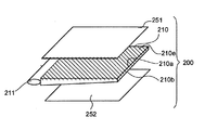
バックライト200は、液晶パネル100の第2面100b側に光出射面210aを向ける断面楔型の矩形のガラス導光板210と、ガラス導光板210の側部に配置されガラス導光板210に光を入射するUV光源211と、液晶パネル100とガラス導光板210との間に矩形状のシート状光学部品としてのプリズムシート251と、ガラス導光板210の光出射面210aと、対抗する面210bと隣り合って配置された矩形状のシート状光学製品としての第1の反射板252とさらにその外側に第2の反射板253とを有する。UV光源211は、直接プリント基板に電気的に接続されている。
【0087】
第1の反射板252と第2の反射板253は、UV光源211からでる光をガラス導光板210に反射させるためのものである。また、プリズムシート251は、出射光の配向角を調整し、正面の輝度を向上させるためのものである。
【0088】
(バックライトの構造)
次にバックライト200について図3及び図4を用いて説明する。図3は、本発明の実施の形態に係るバックライトの概略分解斜視図であり、図4は、図3に示したバックライトの断面図である。
【0089】
バックライト200は、液晶パネル100の第2面100b側に光出射面210aを向ける断面楔型の矩形のガラス導光板210と、ガラス導光板210の側部に配置されガラス導光板210に光を入射するUV光源211と、液晶パネル100とガラス導光板210との間に矩形状のシート状光学部品としてのプリズムシート251と、ガラス導光板210の光出射面210aと、対抗する面210bと隣り合って配置された矩形状のシート状光学製品としての第1の反射板252とを有する。
【0090】
従来の光源として用いられていた蛍光管は、外部にインバータなどの駆動装置を用いていたが、本発明に使用のUV光源211は、プリント基板に電気的に直接接続されているため駆動装置などが不要である。このような構成により、液晶装置1の光源を駆動させる装置を新たに設ける必要がないので、小型化が可能となる。
【0091】
また、UV光源211のUV光は演色性に優れている。このUV光は、UV光源211からガラス導光板210へ入射され、さらにガラス導光板210から基板に挟持された電気光学物質としての液晶5に対してこのUVによって励起された蛍光体の発する白色光等光が出射される。これにより、液晶パネル100の画面が演色性の優れた表示が可能となる。
【0092】
導光板は、光源からの光を受けそしてその光を基板へ向けて出射する領域である。本発明の光源は演色性の優れるが非常に強いUV光を採用しているために従来のプラスチック製の導光板では劣化が進む。そこで、本発明はUV光源211に対応してUV光に強いガラス製の導光板を用いることによって、ガラス導光板210の長期使用を可能とする。
【0093】
液晶装置100におけるガラス導光板210の光出射面210aには、蛍光体210eを塗布する。この蛍光体210eから演色性の優れた白色光を出射することができる。また、プリズムシート251は、液晶パネル100とガラス導光板210の蛍光体210eが塗布された光出射面210aとの間に介在している。プリズムシート251は、UV光源211や蛍光体210eからの出射光の法線方向の強度を調整する。さらに、ガラス導光板210の蛍光体210eが塗布された対向する面210bの外側には第1の反射板252が存在する。この第1の反射弁252は、ガラス導光板210内に入射された光を反射する。これによって、UV光源211から入射した蛍光体210eからの白色光等を効果的に液晶5に対して出射することができる。つまり、これらのプリズムシート251と蛍光体210eと第1の反射板252によって、液晶パネル100を構成する基板を高輝度で表示することができる。
【0094】
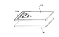
また、図5と図6において、スリット252aと第2の反射板253をさらに具備したバックライト200について説明する。
【0095】
図5では、図4におけるバックライト200にさらにスリット252aと第2の反射板253を具備した断面図について示し、図6では、第1の反射板252と第2の反射板253とスリット252aとの概略分解斜視図について示している。
【0096】
第1の反射板252はUV光源211に近づくにつれて強い光が入射されかつ反射率は高い。つまり、ガラス導光板210は、第1の反射板252から反射されるUV光はUV光源211に近い側ほど強い。また逆にUV光源211から遠ざかるにつれて弱い光となり反射率は低くなる。これにより、ガラス導光板210は、第1の反射板252から反射されるUV光はUV光源211に遠い側ほど弱い。これによって、ガラス導光板210へ第1の反射板252から均一な光量で反射させるのは非常に難しい。そこで、図6に示すように第1の反射板252から出射する光量を均一とするために、UV光源211近くになるにつれてスリット252aをより多く設ける。これによって、第1の反射板252上のUV光源211近くにスリット252aを多く設けることにより反射面積を減らすことができる。そこで、反射する光の量を調整することができる。また、UV光の弱い領域はスリット252aを設けない。つまり、光量の弱い領域はそのままに保ち、光量の強い領域をスリット252aを設けることにより弱めて、均一な光量をガラス導光板210に反射するようにすることができる。また、図5または図6に示すように第1の反射板252の外側に第2の反射板253をさらに設けた。これにより、第1の反射板252のスリット252aより漏れた光をさらに外側に具備された第2の反射板253で反射することができる。このような構成によれば、第1の反射板252のスリット等の光透過領域より漏れた光をさらに外側に具備された第2の反射板253で反射することにより、第1の反射板252との反射率の差を利用して、前記蛍光体を塗布した面の輝度を均一に保つことができる。これによって、2枚の反射板253より出射する光量を制御し電気光学物質に対してより均一に保つことができる。この2枚の反射板は便宜上板状で説明をしているが反射膜または反射層であってもかまわない。また、スリット252aはUV光源211に近づくにつれて多く存在するので、第1の反射板252から漏れたUV光が第2の反射板253で反射されたからといって、必ずしも全てがガラス導光板210に反射されるわけではない。つまり、第2の反射板253面上で反射された光が、第1の反射板252のスリット252aを通過しない限りガラス導光板210に戻ることはない。第1の反射板252のスリット252aから漏出したUV光は第2の反射板253で反射され、ガラス導光板210へ向かおうとする。このようにして、全ての第1の反射板のスリット252aから漏出したUV光を無駄にはせず、2種の反射板の反射率差を利用してより均一になるように調整を行う。
【0097】
図7においては、ガラス導光板210内にバブル210cが設けられている図を示す。ガラス導光板210内にはバブル210cがあり、そのバブル210cはエアーで形成されており、ガラス導光板210内へ入射された光とぶつかる。そして、入射光とバブル210cとがぶつかることによって、光の多重散乱を起こすことができる。これによって、ガラス導光板210内に入射される光を多重散乱させる。つまり、ガラス導光板210に反射する光を偏らないようにすることができ、光量の均一化をはかることが可能となる。
【0098】
図8においては、ガラス導光板210は第1の反射板252と接触する面をフロスト加工する図を示す。ガラス導光板210を第1の反射板252と接触する面をフロスト加工する。それによって、ガラス導光板210からの光が直接的に第1の反射板252に入射せずに、光が乱反射を起こしながら第1の反射板252に入射される。これによって、第1の反射板252へ入射される光は乱反射により偏りが減少し、第1の反射板252上で反射する場合に関してもその偏りが減少した状態で反射される。つまり、第1の反射板252から液晶5へ反射され向かう光は偏りを減少させた状態で向かうので、均一な光量に近づくことができる。
【0099】
図9は、本発明に係る電子機器の一実施形態である携帯電話機を示す斜視図である。電子機器がUV光源211とUV光に強いガラス製のガラス導光板210を有し、蛍光体210eで白色光を出して演色性を高め、第1の反射板252と光学シートであるプリズムシート251とを設けることにより発光効率を高める。さらに第1の反射板252のスリット252aやガラス導光板210内のバブル210cやガラス導光板210の第1の反射板252と接する面をフロスト加工することにより輝度むらをなくことができる。また、スリット252aを設けることによって、スリット252aから漏出したUV光を第1の反射板252の外側に設けられた第2の反射板253で反射させることもできる。これらの構成によって、演色性もよく発光効率も高く輝度むらも低減し、さらには従来の蛍光管を配置する場合に必要な駆動装置が不要なので、薄型化、軽量化ができる。したがって、品質の優れた電子機器を得ることができ、特に携帯電話などの小型の電子機器に適用することが有効である。
【図面の簡単な説明】
【図1】本発明の実施形態にかかる液晶装置の概略分解斜視図である。
【図2】図1に示した液晶装置の断面図である。
【図3】本発明の実施の形態に係るバックライトの概略分解斜視図である。
【図4】図3に示したバックライトの断面図である。
【図5】本発明に係るバックライトの一実施形態に係る断面図である。
【図6】本発明に係る第1の反射板の一実施形態に係る斜視図である。
【図7】本発明に係るガラス導光板の一実施形態に係る斜視図である。
【図8】本発明に係るバックライトの他の実施形態に係る断面図である。
【図9】本発明に係る電子機器の一実施形態である携帯電話機を示す斜視図である。
【符号の説明】
1 液晶装置
3 第1の基板
4 第2の基板
5 液晶
6a 第1の偏光板
6b 第2の偏光板
7 シール材
12a 第1の透明電極
12b 第2の透明電極
12c 第1の端子
100 液晶パネル
100a 第1の面
100b 第2の面
110 液晶画面
200 バックライト
210 ガラス導光板
210a 光出射面
210b 対抗する面
210c バブル
210d フロスト加工面
210e 蛍光体
211 UV光源
251 プリズムシート
252 第1の反射板
252a スリット
253 第2の反射板
300 携帯電話[0001]
BACKGROUND OF THE INVENTION
The present invention relates to an electro-optical device, a lighting device, and an electronic apparatus.
[0002]
[Prior art]
A transflective liquid crystal device, which is an example of an electro-optical device, includes a liquid crystal panel, which is an example of an electro-optical panel, and a backlight that is disposed adjacent to the liquid crystal panel.
[0003]
The liquid crystal panel includes a pair of substrates, a sealing material formed between the pair of substrates along the outer peripheral portion of the substrate, and a liquid crystal as an electro-optical material disposed in a region surrounded by the pair of substrates and the sealing material. And a driving circuit for driving the liquid crystal. For example, the semiconductor device constituting the drive circuit is directly mounted on one of a pair of substrates constituting the liquid crystal panel, or is mounted on a flexible substrate, and the flexible substrate constitutes the liquid crystal panel. It is configured to be electrically connected to one of the pair of substrates.
[0004]
The backlight has a plastic glass light guide plate, a sheet-like optical component stacked on the glass light guide plate, and a light source portion of a fluorescent tube that allows light to enter the glass light guide plate from the side of the glass light guide plate. The fluorescent tube is driven by an external inverter and makes light incident on the glass light guide plate. The glass light guide plate has a shape that is slightly larger in plan view than a region where the liquid crystal of the liquid crystal panel is sandwiched, that is, a region substantially corresponding to the display region.
[0005]
[Problems to be solved by the invention]
However, since the thickness of the light guide plate makes a difference in the luminance of the backlight, for example, when the thickness of the light guide plate is smaller than the lamp diameter of the fluorescent tube (usually 1.5 mm to 3 mm), the luminance decreases sharply. To do. One reason for this is that when the light of the lamp that has come out on the opposite side of the light guide plate is reflected back to the first reflecting plate, it is blocked by the lamp itself of the fluorescent tube and does not enter the light guide plate. As a countermeasure, it is sufficient to increase the thickness of the light guide plate. Furthermore, in order to drive the fluorescent tube, an inverter is required as a drive device, and there is a problem that the liquid crystal device itself becomes large. Further, this fluorescent tube uses a plastic light guide plate as a white light source obtained by applying a fluorescent material on a blue LED chip. However, there is a problem that the light source using the fluorescent tube is subject to color rendering.
[0006]
Accordingly, the present invention has been made in view of the above circumstances, and has been made thinner, lighter, and improved in color rendering, and an electro-optical device, a liquid crystal display device, a lighting device, a lighting device manufacturing method, and an electronic device The purpose is to provide equipment.
[0007]
[Means for Solving the Problems]
In order to solve the above problems, an illumination device of the present invention is an illumination device that is disposed on the back surface of a display panel capable of transmissive display and is used as a backlight, and a surface facing the display panel is defined as a light emitting surface. A light guide surface of the glass light guide plate, a UV light source adjacent to one end face of the side surface of the glass light guide plate, and a reflective plate disposed opposite to the light output surface of the glass light guide plate. The phosphor is applied, and a plurality of bubbles are formed inside the glass light guide plate. The reflection plate includes a reflection region that reflects a part of light from the glass light guide plate, and a glass light guide plate. A light transmission region that transmits a part of the light of the reflection plate, and the reflection region of the reflection plate in the region near the UV light source is smaller than the reflection area of the reflection plate in the region far from the UV light source. Features that are provided To.
[0008]
According to this illuminating device, in the reflector, the light transmission region is provided so that the reflection area in the region near the UV light source is smaller than the reflection area in the region far from the UV light source. The amount of light emitted from the light exit surface is made uniform, and illumination with uniform brightness can be achieved.
Specifically, of the UV light incident from the UV light source, the light that has traveled to the reflector is reflected according to the size of the reflection region, and most of the reflected UV light is excited by the phosphor. It becomes white light.
Here, since the reflection region is formed so as to increase with distance from the UV light source, the amount of UV light directed toward the light exit surface is made uniform, and the amount of white light excited by the phosphor is also substantially reduced. It will be uniform. In addition, since the light passing through the light guide plate is multiply scattered by the plurality of bubbles formed in the light guide plate, the light quantity distribution can be made more uniform.
Furthermore, the UV light source has a simpler driving device than conventional fluorescent tubes, so it can be made compact (thin and light), and white light excited by the phosphor is rich in color rendering. Therefore, it is possible to provide a small illumination device that can perform illumination with uniform brightness and excellent color rendering.
[0009]
According to the illuminating device which concerns on this invention, it is preferable to comprise the optical sheet arrange | positioned facing the light-projection surface of a glass light-guide plate.
Moreover, it is preferable that the light transmission region is formed by slits, and the reflector is provided with more slits toward the UV light source side.
The glass light guide plate is preferably formed by frosting the surface facing the reflector.
[0010]
In order to solve the above problems, an electro-optical device of the present invention includes the above-described illumination device and an electro-optical panel capable of transmissive display, and includes the illumination device as a backlight of the electro-optical panel. And
[0011]
According to such a configuration, white light having excellent color rendering properties is emitted from the phosphor. be able to.
[0012]
According to an aspect of the present invention, it is preferable that an optical sheet is interposed between the second substrate and the phosphor.
[0013]
According to such a configuration, the normal direction of light is adjusted through an optical sheet, for example, a prism sheet. Thereby, the luminance can be increased.
[0014]
According to one form of this invention, it is preferable to comprise a 1st reflecting plate on the outer side of the surface facing the surface which apply | coated the said fluorescent substance of the said glass light-guide plate.
[0015]
According to such a configuration, the light incident on the light guide plate is reflected. Thereby, white light or the like from the phosphor excited by the UV light source can be effectively emitted to the electro-optic material. That is, the substrate constituting the liquid crystal panel can be displayed with high luminance.
[0016]
According to an aspect of the present invention, the light transmission region is formed by a slit, and the first reflecting plate is provided with more slits toward the UV light source.
[0017]
According to such a configuration, strong light is incident on the first reflecting plate as it approaches the UV light source and the reflectance becomes high, and conversely, the light becomes weak as the distance from the UV light source decreases, and the reflectance becomes low. Since the amount of light emitted from the reflector to the electro-optical material becomes too strong as it approaches the UV light source, the amount of light reflected is adjusted by providing more light transmission regions such as slits near the UV light source. Accordingly, the amount of light emitted from the reflecting plate to the electro-optical material can be kept uniform by reducing the amount of light in the strong region incident on the reflecting plate and leaving the region where the incident light is weak.
[0018]
According to an aspect of the present invention, it is preferable that the first reflecting plate further includes a second reflecting plate on a surface side facing the surface adjacent to the glass light guide plate.
[0019]
According to such a configuration, the light that has leaked from the light transmission region such as the slit of the first reflecting plate is reflected by the second reflecting plate that is further provided on the outer side, thereby being reflected from the first reflecting plate. Utilizing the difference in rate, the luminance of the surface coated with the phosphor can be kept uniform. As a result, the amount of light emitted from the two reflectors can be kept more uniform with respect to the electro-optic material.
[0020]
Further, the efficiency is very good by using the light amount leaked from the light transmission region such as the slit of the first reflecting plate without waste.
[0021]
According to one form of this invention, it is preferable that the glass light-guide plate is equipped with the bubble.
[0022]
According to such a configuration, multiple scattering of light occurs when light collides with regions having different refractive indexes such as bubbles in the glass light guide plate. Thereby, the straightness of the light incident on the glass light guide plate from the UV light source side is prevented, and the phosphor can be effectively filled with ultraviolet rays, so that the light utilization rate can be increased.
[0023]
According to one form of this invention, it is preferable that the said glass light-guide plate carries out the frost process of the surface which contacts a said 1st reflecting plate.
[0024]
According to such a configuration, by forming a diffusing surface such as frost processing on the surface where the glass light guide plate is in contact with the first reflecting plate, light is not incident directly on the first reflecting plate but diffusely reflected. The light is incident on the first reflecting plate. As a result, the light traveling from the first reflecting plate to the electro-optic material can be uniformly directed onto the substrate while causing irregular reflection.
[0025]
The liquid crystal display device of the present invention includes a first glass substrate, a second glass substrate disposed at a position facing the first glass substrate, the first glass substrate, and the second glass substrate. It is preferable to include a sandwiched liquid crystal, a glass light guide plate that is adjacent to the second glass substrate and emits light to the liquid crystal, and a UV light source that is adjacent to the light guide region of the glass light guide plate.
[0026]
According to such a configuration, the UV light of the UV light source is excellent in color rendering. As a result, the UV light is incident on the glass light guide plate from the UV light source, and white light emitted by the phosphor excited by the UV light is emitted from the glass light guide plate to the liquid crystal sandwiched between the glass substrates. Thereby, the display surface of the liquid crystal panel of the glass substrate which comprises a liquid crystal panel can be made into the display excellent in color rendering property. Furthermore, an inverter that drives the fluorescent tube is necessary in the fluorescent tube that is a conventional light source, but it is not necessary in the UV light source used in the present invention. Thereby, the thinning and weight reduction of the liquid crystal device can be promoted.
[0027]
In addition, since UV light from the UV light source is incident on the light guide plate, the conventional plastic light guide plate is deteriorated by the UV light, so the glass light guide plate is used. Accordingly, the glass light guide plate can be used for a long time because it is made of glass.
[0028]
According to one form of this invention, it is preferable to apply | coat a fluorescent substance to the adjacent surface of the said 2nd glass substrate of the said glass light-guide plate.
[0029]
According to such a configuration, white light having excellent color rendering properties is emitted from the phosphor. Thereby, the liquid crystal display screen can be displayed with better color rendering.
[0030]
According to an aspect of the present invention, it is preferable that an optical sheet is interposed between the second glass substrate and the phosphor.
[0031]
According to such a configuration, the normal direction of light to the second glass substrate is adjusted via an optical sheet, for example, a prism sheet. Thereby, the brightness of the liquid crystal display screen can be increased.
[0032]
According to one form of this invention, it is preferable to comprise a 1st reflecting plate on the outer side of the surface facing the surface which apply | coated the said fluorescent substance of the said glass light-guide plate.
[0033]
According to such a configuration, the light incident on the light guide plate is reflected. Thereby, white light or the like from the phosphor excited by the UV light source can be effectively emitted to the liquid crystal display screen. That is, the liquid crystal display screen can be displayed with high luminance.
[0034]
According to one form of this invention, it is preferable that the said 1st reflecting plate is equipped with more slits as it goes to the said UV light source side.
[0035]
According to such a configuration, strong light is incident on the first reflector as it approaches the UV light source, and the reflectivity increases. Conversely, as the distance from the UV light source increases, the light becomes weak and the reflectivity decreases. More light transmission regions such as slits are provided near the UV light source so that the amount of light emitted from the first reflector to the liquid crystal does not become too strong as it approaches the UV light source. Accordingly, the light intensity of the strong region incident on the first reflector is reduced by providing a light transmission region such as a slit, and the weak region of the incident light is kept as it is. The amount of light emitted from the reflector to the liquid crystal display screen can be kept uniform.
[0036]
According to an aspect of the present invention, it is preferable that the first reflecting plate further includes a second reflecting plate on a surface side facing the surface adjacent to the glass light guide plate.
[0037]
According to such a configuration, the light that has leaked from the light transmission region such as the slit of the first reflecting plate is reflected by the second reflecting plate that is further provided on the outer side, thereby being reflected from the first reflecting plate. Utilizing the difference in rate, the luminance of the surface coated with the phosphor can be kept uniform.
[0038]
Further, the efficiency is very good by using the light amount leaked from the light transmission region such as the slit of the first reflecting plate without waste.
[0039]
According to one form of this invention, it is preferable that the glass light-guide plate is equipped with the bubble.
[0040]
According to such a configuration, multiple scattering of light occurs when light collides with regions having different refractive indexes such as bubbles in the glass light guide plate. Thereby, the straightness of the light incident on the glass light guide plate from the UV light source side can be prevented, and the phosphor can be effectively filled with ultraviolet rays, so that the light utilization efficiency can be increased.
[0041]
According to one form of this invention, it is preferable that the said glass light-guide plate carries out the frost process of the surface which contacts a said 1st reflecting plate.
[0042]
According to such a configuration, the light is not directly incident on the first reflecting plate by forming a diffusing surface such as frost processing on the surface of the glass light guide plate that contacts the first reflecting plate, The light is incident on the first reflecting plate while causing irregular reflection. As a result, the light traveling from the first reflecting plate toward the liquid crystal display screen is diffusely reflected and can be uniformly directed onto the glass substrate, and the brightness difference of light that may occur because the UV light source is installed on one side is reduced. be able to.
[0043]
The illuminating device of the present invention includes a glass light guide plate that emits light to a member to be illuminated, and a UV light source adjacent to the glass light guide plate.
[0044]
According to such a configuration, the UV light of the UV light source is excellent in color rendering. As a result, the UV light is incident on the glass light guide plate from the UV light source, and the white light emitted from the phosphor excited by the UV light is emitted from the glass light guide plate to the illuminated member. The illumination member can be irradiated with light having excellent color rendering properties. Furthermore, an inverter that drives the fluorescent tube is necessary in the fluorescent tube that is a conventional light source, but it is not necessary in the UV light source used in the present invention. Thereby, thickness reduction and weight reduction of an illuminating device can be promoted.
[0045]
In addition, since UV light from the UV light source is incident on the light guide plate, the conventional plastic light guide plate is deteriorated by the UV light, so the glass light guide plate is used. Accordingly, since the glass is strong against UV, the glass light guide plate can be used for a long time.
[0046]
According to an aspect of the present invention, the phosphor is applied to the light emitting surface that emits light adjacent to the surface of the glass light guide plate facing the UV light source.
[0047]
According to such a configuration, white light having excellent color rendering properties is emitted from the phosphor. As a result, the member to be illuminated can be displayed in a state where the color rendering property is better.
[0048]
According to one form of this invention, it comprises the optical sheet facing the said light-projection surface of the said glass light-guide plate, It is characterized by the above-mentioned.
[0049]
According to such a structure, the normal line direction of the light with respect to a to-be-illuminated member is adjusted through an optical sheet, for example, a prism sheet. As a result, light from the UV light source or the fluorescent material is reflected by the prism sheet, so that the light emission efficiency can be increased, thereby reducing the power consumption.
[0050]
According to an aspect of the present invention, the glass light guide plate includes a first reflecting plate facing the surface opposite to the light emitting surface.
[0051]
According to such a configuration, the light incident on the light guide plate is reflected. Thereby, white light or the like from the phosphor excited by the UV light source can be effectively emitted to the liquid crystal display screen. That is, the liquid crystal display screen can be displayed with high luminance, and further, the light emission efficiency can be increased and the power consumption can be reduced.
[0052]
According to an aspect of the present invention, the first reflecting plate includes a plurality of slits provided toward the UV light source side.
[0053]
According to such a configuration, strong light is incident on the first reflector as it approaches the UV light source, and the reflectivity increases. Conversely, as the distance from the UV light source increases, the light becomes weak and the reflectivity decreases. More light transmission regions such as slits are provided near the UV light source so that the amount of light emitted from the first reflecting plate to the illuminated member does not become too strong as it approaches the UV light source. As a result, the amount of light in the strong region incident on the first reflector is reduced by reducing the area where light can be reflected by providing a light transmission region such as a slit, and the region where the incident light is weak is kept as it is. Thus, the amount of light emitted from the first reflecting plate to the illuminated member can be kept uniform.
[0054]
According to an aspect of the present invention, a second reflecting plate is further provided on the opposite side of the surface of the first reflecting plate facing the glass light guide plate.
[0055]
According to such a configuration, the light leaked from the light transmission region such as the slit of the first reflecting plate is reflected by the second reflecting plate provided further outside, thereby reflecting the first reflecting plate. Utilizing the difference in rate, the luminance of the surface coated with the phosphor can be kept uniform. Further, since the light reflected from the second reflecting plate returns toward the illuminated member from the light transmission region such as the slit of the first reflecting plate, not all the reflected light necessarily returns. As a result, the amount of light emitted from the two reflectors can be kept more uniform with respect to the illuminated member. The two reflecting plates are described as a plate for convenience, but may be a reflecting film or a reflecting layer.
[0056]
Further, the efficiency is very good by using the light amount leaked from the light transmission region such as the slit of the first reflecting plate without waste.
[0057]
According to an aspect of the present invention, the glass light guide plate includes bubbles.
[0058]
According to such a configuration, multiple scattering of light occurs when light collides with regions having different refractive indexes such as bubbles in the glass light guide plate. Thereby, the straightness of the light incident on the glass light guide plate from the UV light source side can be prevented, and the phosphor can be effectively filled with ultraviolet rays, so that the light utilization efficiency can be increased.
[0059]
According to one form of this invention, the said glass light-guide plate carries out the frost process of the surface facing a said 1st reflecting plate, It is characterized by the above-mentioned.
[0060]
According to such a configuration, the light is not directly incident on the first reflecting plate by disposing a diffusing surface such as frost processing on the surface of the glass light guide plate that contacts the first reflecting plate, The light is incident on the first reflecting plate while causing irregular reflection. As a result, the light traveling from the first reflector to the liquid crystal display screen is diffusely reflected so that the amount of light can be uniformly directed on the glass substrate, and the luminance of light that can occur because the UV light source is installed on one side. The difference can be reduced.
[0061]
In the manufacturing method of the lighting device according to the present invention, it is preferable that a glass light guide plate that emits light is disposed on the member to be illuminated, and a UV light source is disposed adjacent to the light guide region of the glass light guide plate.
[0062]
According to such a configuration, since the UV light source can be driven independently, it is not necessary to provide a driving device outside. As a result, it is possible to save the trouble of arranging a driving device or the like in a conventional fluorescent tube, or to manufacture a compact lighting device.
[0063]
According to one form of this invention, it further comprises the process of apply | coating fluorescent substance to the surface which adjoins the surface which installs the said UV light source of the said glass light-guide plate, and radiate | emits light.
[0064]
According to such a configuration, conversion of the UV light source into white light is smooth, and an illumination device with high luminance efficiency can be manufactured.
[0065]
According to an aspect of the present invention, it is preferable that an optical sheet is further provided outside the phosphor.
[0066]
According to such a configuration, white light from the illumination device travels toward the member to be illuminated while adjusting the normal direction. As a result, light with high intensity is emitted to the surface of the member to be illuminated, so that the luminance efficiency can be increased.
[0067]
According to one form of this invention, it is preferable to comprise a 1st reflecting plate on the outer side of the surface facing the surface which apply | coated the said fluorescent substance of the said glass light-guide plate.
[0068]
According to such a configuration, when the UV light from the UV light source or the light from the phosphor is directed to the side of the light guide plate facing the illuminated member side, the light as described above is reflected by the first reflecting plate. Then, the light is emitted toward the illuminated member. As a result, light that has not been directed toward the illuminated member can also be directed by using the first reflector.
[0069]
According to an aspect of the present invention, the first reflecting plate includes a step of providing more slits toward the UV light source side.
[0070]
According to such a configuration, strong light is incident on the first reflector as it approaches the UV light source, and the reflectivity increases. Conversely, as the distance from the UV light source increases, the light becomes weak and the reflectivity decreases. More light transmission regions such as slits are provided on the second reflector near the UV light source so as to emit a uniform amount of light to the illuminated member. As a result, it is possible to manufacture the member to be illuminated with reduced luminance unevenness.
[0071]
According to an aspect of the present invention, it is preferable that the first reflecting plate further includes a second reflecting plate on a surface side facing the surface adjacent to the glass light guide plate.
[0072]
According to such a configuration, the light leaking from the light transmission region such as the slit of the first reflecting plate reaches the second reflecting plate and is reflected toward the first reflecting plate. Further, the reflected light passes through a light transmission region such as a slit on the first reflecting plate and travels toward the light guide plate. At this time, the first reflection plate has more light transmission areas such as slits as it goes to the UV light source side, and conversely, the light transmission areas such as slits decrease as it moves away from the UV light source. The incident light leaked from the light transmission region such as the light does not go to the light guide plate as reflected light. As a result, not all of the light leaked from the light transmission region such as the slit of the first reflecting plate is lost, but a part of the light can be emitted to the light guide plate as reflected light. That is, a part of the light leaked from the light transmission region such as the slit is used while substantially maintaining the uniformity of the amount of light to the illuminated member, so that the waste of manufacturing can be slightly reduced.
[0073]
According to one form of this invention, it is preferable that the glass light-guide plate is equipped with the bubble.
[0074]
According to such a configuration, multiple scattering of light occurs when light collides with regions having different refractive indexes such as bubbles in the glass light guide plate. Thereby, the straightness of the light incident on the glass light guide plate from the UV light source side can be prevented, and the phosphor can be effectively filled with ultraviolet rays, so that the light utilization efficiency can be increased.
[0075]
According to one form of this invention, it is preferable that the said glass light-guide plate comprises the process of frosting the surface which contacts a said 1st reflecting plate.
[0076]
According to such a configuration, the light is not directly incident on the first reflecting plate by forming a diffusing surface such as frost processing on the surface of the glass light guide plate that contacts the first reflecting plate, The light is incident on the first reflecting plate while causing irregular reflection. As a result, the light traveling from the first reflector to the member to be illuminated is diffusely reflected so that the amount of light can be uniformly directed on the glass substrate, and the luminance of light that can occur because the UV light source is installed on one side. The difference can be reduced. Thereby, luminance unevenness in manufacturing can be reduced, and efficiency in manufacturing can be increased.
[0077]
An electronic apparatus according to an aspect of the invention includes the electro-optical device described above.
[0078]
According to such a configuration, the electronic apparatus has a glass light guide plate made of glass that is strong against a UV light source and UV light, emits white light with a phosphor, enhances color rendering, and is provided with a reflector and an optical sheet. Luminance unevenness can be eliminated by increasing the luminous efficiency and further frosting the slit of the reflector, the bubble in the glass light guide plate, or the surface of the glass light guide plate that contacts the reflector. As a result, the color rendering property is good, the light emission efficiency is high, the luminance unevenness is reduced, and further, the driving device necessary for arranging the conventional fluorescent tube is unnecessary, so that the thickness and weight can be reduced. Therefore, an electronic device with excellent quality can be obtained, and it is particularly effective to apply to a small electronic device such as a mobile phone.
[0079]
DETAILED DESCRIPTION OF THE INVENTION
Hereinafter, a liquid crystal device as an electro-optical device will be described as an example with reference to the drawings.
[0080]
(Structure of the liquid crystal device)
First, the structure of the liquid crystal device will be described with reference to FIGS. FIG. 1 is a schematic exploded perspective view of a liquid crystal device according to this embodiment, and FIG. 2 is a schematic cross-sectional view of the liquid crystal device.
[0081]
1 and 2, the
[0082]
The
[0083]
On the surface of the second substrate 4 facing the
[0084]
Each of the
[0085]
In the present embodiment, the
[0086]
The
[0087]
The first reflecting
[0088]
(Backlight structure)
Next, the
[0089]
The
[0090]
The fluorescent tube used as a conventional light source used an external drive device such as an inverter. However, since the UV
[0091]
The UV light from the UV
[0092]
The light guide plate is a region that receives light from the light source and emits the light toward the substrate. The light source of the present invention is excellent in color rendering, but uses very strong UV light, so that the conventional plastic light guide plate deteriorates. Therefore, the present invention enables long-term use of the glass
[0093]
A
[0094]
5 and 6, the
[0095]
5 shows a cross-sectional view in which the
[0096]
The
[0097]
In FIG. 7, the figure by which the
[0098]
In FIG. 8, the glass light-
[0099]
FIG. 9 is a perspective view showing a mobile phone which is an embodiment of the electronic apparatus according to the present invention. The electronic device has a
[Brief description of the drawings]
FIG. 1 is a schematic exploded perspective view of a liquid crystal device according to an embodiment of the present invention.
FIG. 2 is a cross-sectional view of the liquid crystal device shown in FIG.
FIG. 3 is a schematic exploded perspective view of a backlight according to an embodiment of the present invention.
4 is a cross-sectional view of the backlight shown in FIG.
FIG. 5 is a cross-sectional view according to an embodiment of a backlight according to the present invention.
FIG. 6 is a perspective view according to an embodiment of the first reflecting plate according to the present invention.
FIG. 7 is a perspective view according to an embodiment of a glass light guide plate according to the present invention.
FIG. 8 is a cross-sectional view according to another embodiment of a backlight according to the present invention.
FIG. 9 is a perspective view showing a mobile phone which is an embodiment of an electronic apparatus according to the invention.
[Explanation of symbols]
1 Liquid crystal device
3 First substrate
4 Second substrate
5 Liquid crystal
6a First polarizing plate
6b Second polarizing plate
7 Sealing material
12a First transparent electrode
12b Second transparent electrode
12c first terminal
100 LCD panel
100a first side
100b second side
110 LCD screen
200 Backlight
210 glass light guide plate
210a Light exit surface
210b Opposing surface
210c bubble
210d Frosted surface
210e phosphor
211 UV light source
251 Prism sheet
252 First reflector
252a slit
253 Second reflector
300 mobile phone
Claims (5)
前記表示パネルに相対する面を光出射面としたガラス導光板と、
前記ガラス導光板の側面における一端面に隣接したUV光源と、
前記ガラス導光板の前記光出射面の反対面に対向配置された反射板と、を含み、
前記ガラス導光板の前記光出射面には、蛍光体が塗布されるとともに、前記ガラス導光板の内部には、複数のバブルが形成され、
前記反射板は、前記ガラス導光板からの光の一部を反射する反射領域と、前記ガラス導光板からの光の一部を透過する光透過領域とを備え、
前記反射板の前記UV光源から近い領域の反射面積が、前記反射板の前記UV光源から遠い領域の反射面積よりも小さくなるように、前記光透過領域が設けられていることを特徴とする照明装置。An illumination device that is disposed on the back of a display panel capable of transmissive display and is used as a backlight,
A glass light guide plate having a surface facing the display panel as a light exit surface;
A UV light source adjacent to one end surface of the side surface of the glass light guide plate;
A reflector disposed opposite to the surface opposite to the light exit surface of the glass light guide plate,
A phosphor is applied to the light exit surface of the glass light guide plate, and a plurality of bubbles are formed inside the glass light guide plate,
The reflection plate includes a reflection region that reflects a part of light from the glass light guide plate, and a light transmission region that transmits a part of light from the glass light guide plate,
The illumination is characterized in that the light transmission region is provided so that a reflection area of a region near the UV light source of the reflection plate is smaller than a reflection area of a region of the reflection plate far from the UV light source. apparatus.
前記反射板には、前記スリットが前記UV光源側に向かうにつれて多く設けられていることを特徴とする請求項1または請求項2に記載の照明装置。The light transmission region is formed by a slit,
The lighting device according to claim 1, wherein the reflector is provided with more slits toward the UV light source side.
透過表示が可能な電気光学パネルと、を含み、
前記電気光学パネルのバックライトとして前記照明装置を備えることを特徴とする電気光学装置。The lighting device according to any one of claims 1 to 4,
An electro-optical panel capable of transmissive display, and
An electro-optical device comprising the illumination device as a backlight of the electro-optical panel.
Priority Applications (1)
| Application Number | Priority Date | Filing Date | Title |
|---|---|---|---|
| JP2001322800A JP3937797B2 (en) | 2001-10-19 | 2001-10-19 | Electro-optical device and electronic apparatus |
Applications Claiming Priority (1)
| Application Number | Priority Date | Filing Date | Title |
|---|---|---|---|
| JP2001322800A JP3937797B2 (en) | 2001-10-19 | 2001-10-19 | Electro-optical device and electronic apparatus |
Publications (3)
| Publication Number | Publication Date |
|---|---|
| JP2003131221A JP2003131221A (en) | 2003-05-08 |
| JP2003131221A5 JP2003131221A5 (en) | 2005-06-30 |
| JP3937797B2 true JP3937797B2 (en) | 2007-06-27 |
Family
ID=19139781
Family Applications (1)
| Application Number | Title | Priority Date | Filing Date |
|---|---|---|---|
| JP2001322800A Expired - Fee Related JP3937797B2 (en) | 2001-10-19 | 2001-10-19 | Electro-optical device and electronic apparatus |
Country Status (1)
| Country | Link |
|---|---|
| JP (1) | JP3937797B2 (en) |
Families Citing this family (4)
| Publication number | Priority date | Publication date | Assignee | Title |
|---|---|---|---|---|
| JP5783827B2 (en) * | 2011-07-15 | 2015-09-24 | キヤノン株式会社 | LIGHTING DEVICE, ITS CONTROL METHOD, AND DISPLAY DEVICE |
| CN102829393B (en) * | 2012-08-01 | 2015-04-15 | 深圳市华星光电技术有限公司 | Illuminating component |
| CN105393166B (en) | 2014-03-07 | 2019-01-15 | 堺显示器制品株式会社 | Display device |
| JP6787566B2 (en) * | 2016-07-13 | 2020-11-18 | 富士通コネクテッドテクノロジーズ株式会社 | Electronic device equipped with biometric authentication device and biometric authentication device |
-
2001
- 2001-10-19 JP JP2001322800A patent/JP3937797B2/en not_active Expired - Fee Related
Also Published As
| Publication number | Publication date |
|---|---|
| JP2003131221A (en) | 2003-05-08 |
Similar Documents
| Publication | Publication Date | Title |
|---|---|---|
| US7139048B2 (en) | Backlight assembly and liquid crystal display apparatus comprising a light guide plate having light source receiving recess and light guiding recess | |
| KR101331907B1 (en) | Back light unit and liquid crystal display device having thereof | |
| JP4604801B2 (en) | Planar light source device and display device using the same | |
| US9638956B2 (en) | Backlight unit and display apparatus thereof | |
| US20070064444A1 (en) | Display device | |
| US6554440B2 (en) | Light pipe, plane light source unit and liquid-crystal display device | |
| KR20050055387A (en) | Liquid crystal display module | |
| JP2004311353A (en) | Surface light source device and liquid crystal display device using this device | |
| WO2000032981A9 (en) | Illuminator, illuminating device, front light, and liquid crystal display | |
| WO2011135627A1 (en) | Planar light source apparatus and display apparatus using same | |
| US20150253484A1 (en) | Illumination device and display device | |
| JP2006106736A (en) | Optical film, backlight assembly having same and display device having same | |
| US8810749B2 (en) | Backlight sources having reduced thickness and liquid crystal display device using the same | |
| JP2007094253A (en) | Electrooptical apparatus, electronic device, and manufacturing method of electrooptical apparatus | |
| US8400581B2 (en) | Back light unit and liquid crystal display comprising the same | |
| KR101540216B1 (en) | Optical member and display device having the same | |
| KR20060029391A (en) | Optical film, and backlight assembly and display device having the same | |
| JP2006066120A (en) | Light source device, electro-optical device, and electronic apparatus | |
| KR20070108991A (en) | Backlight assembly and liquid crystal display using the same | |
| KR101186868B1 (en) | Back light and liquid crystal display device having thereof | |
| JP3937797B2 (en) | Electro-optical device and electronic apparatus | |
| KR20140067471A (en) | Diffusing light guide film, backlight unit, and liquid crystal display device having thereof | |
| KR100710281B1 (en) | Optical Reflective Diffusing Plate and Liquid Crystal Display Module Using the Same | |
| KR20060131243A (en) | Back light assembly and display apparatus having the same | |
| JP2002229019A (en) | Reflection-type liquid crystal display and auxiliary light source device |
Legal Events
| Date | Code | Title | Description |
|---|---|---|---|
| A521 | Written amendment |
Free format text: JAPANESE INTERMEDIATE CODE: A523 Effective date: 20041012 |
|
| A621 | Written request for application examination |
Free format text: JAPANESE INTERMEDIATE CODE: A621 Effective date: 20041012 |
|
| A977 | Report on retrieval |
Free format text: JAPANESE INTERMEDIATE CODE: A971007 Effective date: 20060801 |
|
| A131 | Notification of reasons for refusal |
Free format text: JAPANESE INTERMEDIATE CODE: A131 Effective date: 20060808 |
|
| A521 | Written amendment |
Free format text: JAPANESE INTERMEDIATE CODE: A523 Effective date: 20061006 |
|
| A02 | Decision of refusal |
Free format text: JAPANESE INTERMEDIATE CODE: A02 Effective date: 20061212 |
|
| A521 | Written amendment |
Free format text: JAPANESE INTERMEDIATE CODE: A523 Effective date: 20070208 |
|
| A911 | Transfer of reconsideration by examiner before appeal (zenchi) |
Free format text: JAPANESE INTERMEDIATE CODE: A911 Effective date: 20070214 |
|
| TRDD | Decision of grant or rejection written | ||
| A01 | Written decision to grant a patent or to grant a registration (utility model) |
Free format text: JAPANESE INTERMEDIATE CODE: A01 Effective date: 20070306 |
|
| A61 | First payment of annual fees (during grant procedure) |
Free format text: JAPANESE INTERMEDIATE CODE: A61 Effective date: 20070319 |
|
| R150 | Certificate of patent or registration of utility model |
Free format text: JAPANESE INTERMEDIATE CODE: R150 |
|
| FPAY | Renewal fee payment (event date is renewal date of database) |
Free format text: PAYMENT UNTIL: 20110406 Year of fee payment: 4 |
|
| FPAY | Renewal fee payment (event date is renewal date of database) |
Free format text: PAYMENT UNTIL: 20110406 Year of fee payment: 4 |
|
| FPAY | Renewal fee payment (event date is renewal date of database) |
Free format text: PAYMENT UNTIL: 20120406 Year of fee payment: 5 |
|
| FPAY | Renewal fee payment (event date is renewal date of database) |
Free format text: PAYMENT UNTIL: 20130406 Year of fee payment: 6 |
|
| FPAY | Renewal fee payment (event date is renewal date of database) |
Free format text: PAYMENT UNTIL: 20130406 Year of fee payment: 6 |
|
| FPAY | Renewal fee payment (event date is renewal date of database) |
Free format text: PAYMENT UNTIL: 20140406 Year of fee payment: 7 |
|
| S531 | Written request for registration of change of domicile |
Free format text: JAPANESE INTERMEDIATE CODE: R313531 |
|
| R350 | Written notification of registration of transfer |
Free format text: JAPANESE INTERMEDIATE CODE: R350 |
|
| LAPS | Cancellation because of no payment of annual fees |