JP3920249B2 - Optical waveguide - Google Patents
Optical waveguide Download PDFInfo
- Publication number
- JP3920249B2 JP3920249B2 JP2003196759A JP2003196759A JP3920249B2 JP 3920249 B2 JP3920249 B2 JP 3920249B2 JP 2003196759 A JP2003196759 A JP 2003196759A JP 2003196759 A JP2003196759 A JP 2003196759A JP 3920249 B2 JP3920249 B2 JP 3920249B2
- Authority
- JP
- Japan
- Prior art keywords
- optical waveguide
- substrate
- micromirror
- light
- optical
- Prior art date
- Legal status (The legal status is an assumption and is not a legal conclusion. Google has not performed a legal analysis and makes no representation as to the accuracy of the status listed.)
- Expired - Fee Related
Links
Images


Landscapes
- Optical Integrated Circuits (AREA)
Description
【0001】
【発明の属する技術分野】
本発明は、集積回路間を接続するために用いられる光導波路およびその製造方法、ならびに、光導波路を用いて光信号を伝搬する光情報処理装置に関する。
【0002】
【従来技術】
複数の集積回路間での信号の送受信のために、電気信号を一旦光信号に変換し、光信号で送受信する光インターコネクション(内部光結合)の技術として、文献Jpn.J.Appl.Phys.Vol.36(1997)pp.1903−1906では、基板上の光導波路を用いて電気信号を伝搬する構成が開示されている。この構成では、LSI基板に、電気信号と光信号との変換のための発光ダイオードおよび受光素子を取り付け、このLSI基板を光導波路が形成された基板上に搭載している。そして、光導波路を伝搬する光信号を、光導波路内のマイクロミラーで基板面に垂直な方向に偏向させることにより、光導波路から出射させ、この光信号をLSI基板上の受光素子で受光する。また、発光ダイオードから光導波路に向かって光信号を出射させ、これを光導波路内のマイクロミラーで光導波路の伝搬方向に偏向させ、光導波路を伝搬させる。この光導波路内のマイクロミラーとしては、光導波路の下面上に形成した山型のアルミミラーを用いている。この山型のアルミミラーの斜面で光を反射させて偏向させている。
【0003】
しかしながら、光導波路内のマイクロミラーを効率よく製造する方法は、従来知られていなかった。
【0004】
また、光導波路内にマイクロミラーを多段に配置した場合に、伝搬損失のために後段のマイクロミラーによる反射光強度が減少してしまうという問題もあった。
【0005】
また、上述の光インターコネクションのシステムでは、LSIの入出力信号は光信号に変換されるため、光導波路で伝送できるが、LSIや発光ダイオードや受光素子へは依然として電源電圧を供給する必要がある。このため、電源電圧供給用の配線をどこに配置するのかが問題となる。
【0006】
【発明が解決しようとする課題】
本発明は、伝搬光を基板面の上方に入出射させるために、内部にマイクロミラーを備えた光導波路を容易に製造するための製造方法を提供することを第1の目的とする。
【0007】
本発明は、伝搬光を基板面の上方に入出射させるために、内部に多段のマイクロミラーを備えた光導波路であって、後段のマイクロミラーの反射光強度を一定以上にすることのできる光導波路を提供することを第2の目的とする。
【0008】
本発明は、電気回路と受発光素子とが形成された基板を、光導波路基板上に搭載する構成の光情報処理装置であって、電気回路等への電源供給用配線を、効率よくコンパクトに配置することの可能な光情報処理装置を提供することを第3の目的とする。
【0009】
【課題を解決するための手段】
上記第1の目的を達成するために、本発明によれば、以下のような光導波路の製造方法が提供される。
【0010】
すなわち、側面が傾斜した凸部を、表面に有するクラッド層を基板上に形成する第1の工程と、
前記クラッド層の前記凸部の側面上に、反射膜を形成する第2の工程と、
前記クラッド層の前記凸部の上に、光導波路を形成する第3の工程とを有し、前記第1の工程は、前記側面が傾斜した凸部を形成するために、等方性エッチングを用いることを特徴とするマイクロミラーを備えた光導波路の製造方法である。
【0011】
また、上記第2の目的を達成するために、本発明によれば、以下のような光導波路が提供される。
【0012】
すなわち、基板と、
前記基板上に形成された、側面が傾斜した凸部を複数表面に有すクラッド層と、
前記クラッド層上に形成され光導波路層とを備えており、
前記複数の凸部の斜面の光の進行方向に対して同一側に反射膜が形成された光導波路であって、
前記反射膜は反射膜に到達する光量の減衰度に応じ反射光量が一定になるように調整されていることを特徴とする光導波路である。
【0013】
また、上記第3の目的を達成するために、本発明によれば、以下のような光情報処理装置が提供される。
【0014】
すなわち、光導波路と所定の配線パターンとを備えた導波路基板と、
前記光導波路と対向するように前記導波路基板上に搭載された電気回路基板と、
前記前記導波路基板と前記電気回路基板とを連結する一以上の連結部とを有し、
前記電気回路基板は、前記光導波路を伝搬する光信号を受光するための受光素子と、電気回路とを備え、
前記連結部は、導電性であり、
前記配線パターンは、前記連結部を介して、前記受光素子および電気回路と電気的に接続されていることを特徴とする光情報処理装置である。
【0015】
【発明の実施の形態】
本発明の一実施の形態について、以下図面を用いて説明する。
【0016】
まず、本発明の第1の実施の形態のマイクロミラーを備えた光導波路の製造方法について図1〜図8を用いて説明する。
【0017】
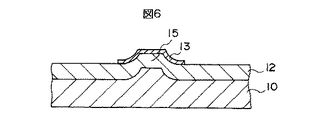
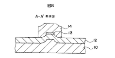
まず、図1のように、シリコン基板10上に厚さ約1μmのレジスト膜11を形成する。具体的には、粘度20cpの感光性樹脂溶液((株)東京応化社製OFPR−800)を1500rpmで2秒、さらに、3000rpmで30秒の条件でスピナーを用いて塗布した後、キュアすることによりレジスト膜11を形成する。その後、露光および現像し、図2のような形状にパターニングする。現像液としては、テトラメチルアンモニウムハイドロオキサイド2.38%を含む現像液((株)東京応化社製NMD−3)を用いる。
【0018】
つぎに、レジスト膜11をマスクとし、シリコン基板10を等方性エッチングするエッチング液を用いてエッチングを行い、シリコン基板10に、高さ約0.5μmの凸部15を形成する(図3)。エッチング液としては、本実施の形態では、HNO3とHFとをHNO3/HF=95/5の割合で混合したものを用いる。このように等方性エッチングを行うと、エッチングがシリコン基板10の厚さ方向の他に横方向にも進行するため、レジスト膜11の下部にもエッチング液が回り込んでアンダーカットが生じる。これにより、形成される凸部15の側面を、ミラー面に適した角度の傾斜面にすることができる。
【0019】
この後、レジスト膜11を取り除き、シリコン基板10の表面全体を1100℃で6時間かけて熱酸化して、厚さ1.2μm程度の酸化膜を形成する(図4)。これにより、前記凸部15の形状にならうように酸化膜を形成することができる。この酸化膜が下部クラッド12となる。さらに、下部クラッド12の上に、厚さ0.2μmのアルミ膜13をスパッタ成膜で形成した(図5)後、アルミ膜13が凸部15の傾斜面を覆うように残し、残りの部分をフォトリソグラフィにより取り除く。これにより、アルミ膜13からなるマイクロミラーを構成することができる。
【0020】
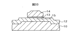
つぎに、下部クラッド12の表面に、厚さが分子オーダーの極薄い有機ジルコニウム化合物の被膜を形成する。このように有機ジルコニウム化合物の被膜を形成するのは、この上に形成するポリイミドの光導波路14と下部クラッド12との密着強度を向上させるためである。そして、日立化成工業(株)社製のOPI−N3505を塗布・ベークして所望の厚さのポリイミド層を形成した後、図8のように、リッジ型導波路形状にドライエッチングによりエッチングし、ポリイミドからなる光導波路14を形成する。なお、図33のように、凸部15の幅およびアルミ膜13の幅を光導波路14の幅と同等かそれ以上に広くした構成にすることもできる。図33の構成の場合、アルミ膜13により偏向される光量が大きくなり、偏向光量を大きくしたい場合の構成として適している。
【0021】
この光導波路14は、図9のように、空気を上部クラッドとして光を伝搬する。伝搬光の一部は、アルミ膜13のマイクロミラーの一方の傾斜面13aにより、シリコン基板10の上方に向かって偏向され、光導波路14から上方に向かって出射される。よって、シリコン基板10の上方に、LSI103、受光素子101および発光ダイオード(LEDの他レーザダイオードなどの発光素子を含む)102を搭載した基板100を配置しておくことにより、光導波路14の伝搬光の一部を、受光素子101で受光することができる。これにより、伝搬光を光信号を電気信号に変換して、LSI103で処理することができる。また、LSI103から出力される電気信号を発光ダイオード102により光信号に変換し、アルミ膜13のマイクロミラーに向かって出射させることにより、アルミ膜13のもう一方の傾斜面13bで反射して、光導波路14の伝搬方向に偏向することできる。これにより、LSI103の出力した電気信号を、光導波路14で伝送することができる。
【0022】
このように、第1の実施の形態の製造方法では、等方性エッチングによるアンダーエッチングを利用することにより、マイクロミラーに適した斜面を持つ凸部を容易に形成することができるため、これに金属膜を被せることにより、マイクロミラーを備えた光導波路14を容易に製造することができる。また、等方性エッチングのエッチング条件を変化させることにより、形成される凸部の形状を制御することができるため、光導波路を伝搬する光のモード等に応じて、凸部の傾斜面の角度を制御し、所望の方向に光を偏向するマイクロミラーを製造することができる。
【0023】
なお、本実施の形態では、マイクロミラーを構成するためにアルミ膜13を用いているが、他の金属、例えばCr,Cu,Au,Agなどの膜を用いることももちろん可能である。また、金属膜以外に、伝搬光を反射する誘電体膜を用いることも可能である。
【0024】
また、光導波路14の屈折率に対して、凸部15の屈折率が小さくなるようにするとともに、凸部15の傾斜面の角度を調整して形成することにより、金属膜等の反射膜を特別に設けることなく、凸部15のみでマイクロミラーを構成することも可能である。この場合、光導波路14の屈折率と凸部15の屈折率とに応じて凸部15の傾斜面の角度を調整することで、全反射のマイクロミラーを構成することが可能である。
【0025】
また、上述の実施の形態では、下部クラッド12を熱酸化による酸化膜で形成しているが、熱酸化の代わりに図4の工程で、基板10上にCVD、スパッタリング等によりSiO2膜等を形成し、これを下部クラッド12にすることも可能である。この場合、厚さの厚い下部クラッド12を容易に形成することができる。また、SOG(Spin On Glass)膜を塗布し硬化させることにより、下部クラッド12を形成することも可能である。さらに、下部クラッド12を、導波路14よりも屈折率の小さい樹脂を用いて形成することもできる。この場合、安価に製造することができる。
【0026】
また、上述の実施の形態では、基板10の表面に凸部15を形成し、これにならうように下部クラッド12を形成することにより、下部クラッド12の表面に凸部15を形成しているが、この方法に限らず、平坦な基板10の上に下部クラッド12を形成した後、下部クラッド12の表面を等方性エッチングすることにより、下部クラッド12の表面に直接凸部を形成することも可能である。
【0027】
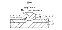
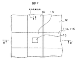
さらに、図9の構成において、LSI103、発光ダイオード102および受光素子101を駆動電流を供給するための電源線やグランド線、ならびに、これらから出力される電気信号を伝達するための電気配線を、後述するように、基板10上に形成することができる。この場合には、アルミ膜13をマイクロミラーの形状にパターニングするのと同時に、電源線、グランド線、配線等の所望の配線パターンにパターニングすることにより、マイクロミラーと配線を一括して製造できる。さらに、図16、図17に示すような形状にアルミ膜13をパターニングすることにより、マイクロミラーを光導波路14を横切る配線の一部にすることも可能である。
【0028】
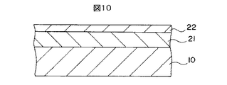
つぎに、本発明の第2の実施の形態のマイクロミラーを備えた光導波路の製造方法について図10〜図13を用いて説明する。
【0029】
本実施の形態では、金属膜を等方性エッチングすることにより、斜面を有するマイクロミラーを形成する。
【0030】
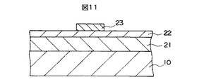
まず、シリコン基板10の上に、SiO2膜を成膜して下部クラッド21を形成した後、さらにアルミ膜22を成膜する(図10)。この上に、レジスト膜23を形成してパターニングする(図11)。このレジスト膜23をマスクとして、アルミ膜22を等方性エッチングするエッチング液を用いてエッチングを行うと、レジスト膜23の下部にもエッチング液が回り込んでアンダーエッチングが生じ、傾斜面を有する凸形状のアルミ膜22のマイクロミラーを形成することができる。この後、第1の実施の形態と同様の方法で、下部クラッド21の表面をOPIカップラで処理した後、ポリイミドの光導波路14を形成する。
【0031】
この方法では、アルミ膜22を直接等方性エッチングするため、下部クラッド21を平坦にすることができ、光導波路14の伝搬効率を高めることができる。
【0032】
また、この方法では、下部クラッド21が平坦であるため、下部クラッド21をポリイミド等の有機樹脂により形成することも可能である。
【0033】
さらに、本発明の第3の実施の形態のマイクロミラーを備えた光導波路の製造方法について説明する。本実施の形態では、異方性エッチングを利用して基板上に傾斜面を有する凸部を形成する。
【0034】
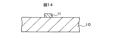
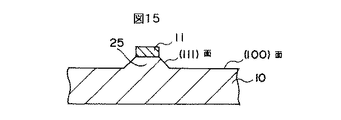
本第3の実施の形態の製造方法は、第1の実施の形態とほぼ同じであるが、シリコン基板10として、基板面が(100)面のものを用いる。このような基板10を用い、図14のようにレジスト膜11を形成し、エッチング液として水酸化カリウム水溶液等を用いると、シリコン結晶の(111)面のエッチング速度が、(100)面のエッチング速度よりも極めて遅いという特性を利用して、側面が(111)面の斜面となる凸部25を形成することができる。これ以降の工程は、第1の実施の形態と同様にする。
【0035】
この方法では、傾斜面である(111)面の角度が基板面の(100)面に対して、54.7°と正確に決定されるため、マイクロミラーの傾斜面のばらつきをなくすことができる。よって、この傾斜面の角度に合わせて、光導波路のモードを設計しておくことにより、精度よく所望の方向に光を偏向することができる。
【0036】
また、上述の各実施の形態の光導波路は、空気を上部クラッドとする構成であったが、図18のように上部クラッド17を備える構成にすることもできる。上部クラッド17としては、スパッタリング法等で形成したSiO2膜や、日立化成工業(株)社製のOPI−N1005を塗布およびベークして形成したポリイミド層等の有機樹脂層を用いることができる。
【0037】
さらに、上述の各実施の形態では、光導波路14の下部に、凸形状のマイクロミラーを構成するため、この部分で光導波路14も凸形状となる。そこで、光導波路14の上面を研磨することにより、図18のように上面が平坦な光導波路14を形成することも可能である。この場合、光導波路14の伝搬損失を低減することができるという効果が得られる。
【0038】
また、上述の第1および第2の実施の形態では、等方性エッチングとして、ウエットエッチングを用いているが、本発明はウエットエッチングに限られるものではなく、アンダーカットが生じる等方性エッチングが行える条件であれば、ドライエッチングを用いることも可能である。
【0039】
つぎに、本発明の第4の実施の形態として、第1の実施の形態の光導波路14を用いて構成した光情報処理システムについて説明する。
【0040】
シリコン基板10には、図19のように、環状の光導波路14が形成されている。また、基板10の上には、合計6枚のLSI基板100、111、112が、光導波路14に沿うように搭載されている。LSI基板100、111、112の基板10に対向する面の四隅には、図21のように、アルミパッド121が形成され、基板10上にも、アルミパッド121と対向する位置にアルミパッド122が形成されている。これらは、クロム膜123および導電性接着剤層142を介して銅バンプ124によって接続されている。これによって、基板100、111、112が、わずかな空隙をあけて基板10上に搭載される。なお、クロム膜123は、銅バンプ124とアルミパッド122との接着強度を高めるために配置されている。
【0041】
また、基板10上には、光導波路14の他に、図19のように、電源用配線113、グランド用配線114、クロック信号用配線115、および、入出力信号配線116、117が形成されている。電源用配線113、グランド用配線114、クロック信号用配線115は、基板100、111、112の下の四隅のアルミパッド122のいずれかにそれぞれ接続されている。また、入力信号配線116は、基板112のアルミパッド122に接続され、出力信号配線117は、基板111のアルミパッド122に接続されている。よって、電源、グランド、クロック信号、入出力信号は、それぞれ、銅バンプ124、アルミパッド121を介して、基板100、111、112に供給される。また、電源用配線113、グランド用配線114、クロック信号用配線115、および、入出力信号配線116、117には、アルミパッド121とは逆側の端部にそれぞれ接続パッド113a,114a,115a,116a,117aが形成されている。接続パッド113aは、電源回路130に接続され、接続パッド114aは、アース131に接続され、接続パッド115aは、クロック回路132に接続されている。また、接続パッド116a、117aは、制御部133に接続されている。なお、図19では、基板10上の配線113等の経路をわかりやすくするために模式的な配線経路にしているが、実際の配線経路は配線113の引き回し等を考慮した効率的な経路にする。また、図19、図21では、図示を省略しているが、配線113等の上には保護膜が形成されている。
【0042】
また、4枚のLSI基板100には、図20のように、発光ダイオード102と受光素子101とLSI103とが搭載されている。また、LSI基板111には、発光ダイオードは搭載されておらず、受光素子101とLSI103とが搭載されている。
【0043】
LSI基板112には、受光素子は搭載されておらず、発光ダイオード102とLSI103とが搭載されている。発光ダイオード102および受光素子101は、それぞれ、図21、図9のように受発光面が光導波路14の真上に位置し、しかも、受発光面が光導波路14を向くように基板100、111、112に搭載されている。
【0044】
LSI基板100には、銅バンプを介して基板10側から供給される電源電圧およびグランド電圧を発光ダイオード102、受光素子101、LSI103に供給するとともに、クロック信号をLSI103に入力するための配線134が配置されている(図22(a))。また、受光素子101の出力をLSI103に入力するための配線134およびLSIの出力を発光ダイオード102に入力するための配線134が配置されている。
【0045】
LSI基板112にも同様に、発光ダイオード102およびLSI103に電源電圧およびグランド電圧を供給するとともに、クロック信号をLSI103に入力するための配線135が形成されている(図22(b))。また、基板112には、受光素子が搭載されていないため、外部の制御部133からの入力信号をLSI103に入力するための配線135も配置されている。LSI基板111にも、受光索子101およびLSI103に電源電圧およびグランド電圧を供給するとともに、クロック信号をLSI103に入力するための配線136が形成されている(図22(c))。また、基板111には、発光素子が搭載されていないため、LSI103の出力信号を外部の制御部133へ出力するための配線136も配置されている。
【0046】
また、光導波路14には、6枚の基板100、111、112と対向する位置に、アルミ膜13からなるマイクロミラーが備えられている(図9)。このマイクロミラーは、光導波路14の光の伝搬方向にそって2つの傾斜面13a,13bを有し、一方の傾斜面13aによって、伝搬光の一部を基板10の上方に偏向する。また、他方の傾斜面13bによって、発光ダイオード102から出射された光を、光導波路14の伝搬方向に偏向し、光導波路14に伝搬させる。
【0047】
つぎに、本実施の形態の光情報処理システムの動作について説明する。
【0048】
電源回路130からの電源電圧は、基板10上の接続パッド113aおよび電源用配線113およびアルミパッド122を通った後、銅バンプ124を通って6枚のLSI基板100、111、112に達し、これらの基板100、111、112上の配線134、135、136によって、発光ダイオード102、受光素子101およびLSI103へ供給される。同様に、グランド電圧も、基板10上の接続パッド114a、グランド用配線114、アルミパッド122、銅バンプ124、アルミパッド121および配線134、135、136を経由して発光ダイオード102、受光素子101およびLSI103へ供給される。クロック回路132から出力されたクロック信号も、同様に、基板上のクロック信号用配線115、銅バンプ124等を経由して、LSI103に供給される。
【0049】
これら電源電圧およびグランド電圧の供給によって、発光ダイオード102および受光素子101は、受発光が可能になる。また、LSI103も動作が可能になる。
【0050】
4枚の基板100上のLSI103は、いずれも受光素子101および発光ダイオード102と接続されているため、他の基板100、111、112のLSI103との間で送受信すべき信号を、すべて光信号に変換して、光導波路14を介して送受信する。ただし、基板111には発光ダイオードは搭載されていないため、基板111のLSI103は、光導波路14を介して他の基板100、112のLSI103から光信号を受光素子101を介して受け取ることはできるが、受け取った信号を演算した結果は、電気信号のまま制御部133に受け渡す。また、基板111には受光素子は搭載されていないため、基板111のLSI103は、制御部133から電気信号として受け取った信号を演算したのち、発光ダイオード102により光信号に変換して他の基板100、111のLSIに出力する。制御部133との電気信号は、銅バンプ124、基板10上の信号用配線116、117を経由して送受信される。
【0051】
本実施の形態では、基板100のLSI103は、選択回路と、演算回路と、信号出力回路とを備える構成にする。選択回路は、受光素子101が受け取った信号から自分に向けられて発信された信号のみを選択する。演算回路は、選択回路が選択した信号を用いて予め定められた演算を行う。そして、信号出力回路は、演算回路の演算結果に、基板111のLSI103を示す宛先信号をつけた信号を作成し、それを発光ダイオード102に光信号として出力させる。
【0052】
また、基板112のLSI103は、情報分割回路と信号出力回路とを備える構成にする。この情報分割回路は、制御部133から受け取った処理すべき情報を、4つの情報に分割し、それぞれの情報を4つの基板100のLSI103にひとつづつ割り当てる。信号出力回路は、分割した情報に割り当てた相手を示す宛先信号をつけた信号を作成し、それを発光ダイオード102に光信号として出力させる。
【0053】
基板111のLSI103は、選択回路と、出力回路とを備える。選択回路は、受光素子101が受け取った信号から自分に向けられて発信された信号のみを選択する。出力回路は、受け取った信号を合成し、制御部133に出力する。
【0054】
これらの動作について具体的に説明する。基板112のLSI103は、図23のように、処理すべき情報を制御部133から電気信号として受け取る。基板112のLSI103の情報分割回路は、受け取った情報を4つの情報に分割し、分割した情報をひとつづつ割り当てる先の基板100を定める。基板112のLSI103の信号出力回路は、4つの情報にそれぞれ割り当て先の基板100を特定する宛先信号をつけた信号を作成し、それを発光ダイオード102に光信号として出力させる。基板112の発光ダイオード102から発せられた光は、基板112の下にあるアルミ膜13からなるマイクロミラーで偏向されることにより、光導波路14の伝搬光となって、光導波路14を伝搬する。
【0055】
4つの情報の光信号は、それぞれ光導波路を伝搬し、基板112に最も近い基板100の下部に到達すると、アルミ膜13からなるマイクロミラーによって伝搬光の一部が図9のように基板10の上方に偏向され、基板100上の受光索子101によって受光され、電気信号に変換され、LSI103に受け渡される。基板100のLSI103の選択回路は、受け取った電気信号のうち、自分宛の情報の信号のみを選択し、演算回路がその情報を演算する。そして、信号出力回路は、演算結果に、基板111のLSI103を示す宛先信号をつけた信号を作成し、それを発光ダイオード102に光信号として出力させる。基板100の発光ダイオード102から発せられた光は、基板100の下にあるアルミ膜13からなるマイクロミラーで偏向されることにより、光導波路14の伝搬光となって、光導波路14を伝搬する。
【0056】
同様に、他の基板100の下部においても、光導波路14を伝搬している光の一部がマイクロミラーによって偏向されることにより、受光素子101によって受光され、基板100のLSI103に受け渡される。基板100のLSI103は、そのうちの自分宛の情報の信号のみを選択して演算し、演算結果に基板111のLSI103を示す宛先信号をつけた信号を作成し、それを発光ダイオード102に光信号として出力させる。この光信号は、光導波路14の伝搬光となって、光導波路14を伝搬する 基板111の下部においても、光導波路14を伝搬している光の一部がマイクロミラーによって偏向されることにより、受光素子101によって受光され、基板111のLSI103に受け渡される。
【0057】
基板111のLSI103の選択回路は、そのうちの自分宛の情報の信号のみを選択することにより、4つの基板100のLSI103がそれぞれ演算した結果を受け取る。そして、この結果を合成することにより所望の演算結果を得て、出力回路が電気信号として制御部133に受け渡す。
【0058】
このように、本実施の形態の光情報処理システムでは、環状の光導波路14を用いているため、情報が光導波路14を環状に循環している。したがって、ある基板から出力された情報を、常に、すべての基板で受信可能な状態にある。よって、LSI基板100、111、112を1対1に光導波路で接続する必要がなく、1本の光導波路14ですべてのLSI基板100、111、112間での信号の送受信が可能になるという利点がある。よって、複雑な光導波路網を形成する必要がない。また、本実施の形態では、6枚の基板100、111、112を搭載しているが、情報処理内容が変更になり、基板を追加する必要が生じた場合にも、光導波路14上のどこかに、追加すべき基板を搭載するだけで、他のすべての基板との間で情報の送受信が可能になる。よって、光導波路14の経路を作り直す必要がなく、容易に情報処理内容の変更を行うことができる。なお、この場合には、追加する基板の位置に、マイクロミラーや電源用配線等が必要があるため、予め基板10上に光導波路14を製造する段階で、基板を追加可能な位置のすべてにマイクロミラーやアルミパッド122を設けておくことが望ましい。この場合、基板が配置されていない位置のマイクロミラーにおいても、伝搬光の一部が偏向され、光の損失となるが、発光ダイオード102の出力光強度を十分大きく設定しておけば問題は生じない。
【0059】
なお、本実施の形態では、LSI基板112が、電気信号で処理すべき情報を受け取って、LSI基板100が分割処理し、LSI基板111で処理結果を合成して出力するという構成を示したが、本発明は、この構成に限定されるものではなく、LSI基板100間で演算結果を送受信する構成にすることももちろん可能である。また、電気信号で処理すべき情報を外部から受け取るのではなく、光導波路14に接続された光導波路から光信号として受け取る構成や、処理結果を光信号として外部に出力する構成にすることも可能である。このように、入出力される情報をすべて光信号にする場合には、LSI基板111、112のように電気信号で情報を入出力させる基板に代えて、すべてのLSI基板を基板100のように、発光ダイオード102および受光素子101を備えた構成にする。
【0060】
また、本実施の形態では、LSI基板100、111、112への電源電圧等の供給を、基板10上に設けた配線113等、ならびに、LSI基板100等を支持するための銅バンプを介して行っている。このような構成にすることにより、発光ダイオード102、受光素子101を下面側に搭載している基板100、111、112等への給電を、フリップ・チップのように下面側から行うことができる。これにより、基板100、111、112の上面側に配線や端子を設ける必要がない。また、基板100、111、112の基板10上への取り付けと、電気的な接続とを銅バンプによって同時に行うことができるため、製造工程が簡単になる。
【0061】
また、基板10上に配線113等を配置することにより、配線113を形成する工程を、アルミ膜13からなるマイクロミラーを形成する工程や、光導波路14等を形成する工程と一連の工程として簡単に形成できるという利点もある。以下、基板10上に、光導波路14、マイクロミラー、および、配線113等を形成する製造工程について説明する。
【0062】
まず、第1の実施の形態で説明した図1〜図6の工程により、図19の基板10上に下部クラッドを形成するとともに、基板100、111、112の下部となる位置にアルミ膜13と凸部15とからなるマイクロミラーを形成する。
【0063】
つぎに、下部クラッド12上にレジスト膜を形成した後、リフトオフ法により配線113、114、115、116、117、アルミパッド122、接続パッド113a、114a、115a、116a、117aを、厚さ0.8μmのアルミ膜によって形成する。さらに、基板10の表面全体に、日立化成工業(株)社製のPIX−1400を塗布およびベークすることにより、表面全体にポリイミドからなる保護膜140を形成する(図14)。その後、ドライエッチングによって、光導波路14を形成すべき領域、アルミパッド122、ならびに、接続パッド113a等の領域から保護膜140を取り除く。
【0064】
つぎに、光導波路14を形成すべき領域の下部クラッド12の表面に、日立化成工業(株)社製のOPIカップラを塗布し、下部クラッド12の表面に、厚さが分子オーダーの極薄いOPIカップラの有機分子膜を形成する。このようにOPIカップラの有機分子膜を形成するのは、この上に形成するポリイミドの光導波路14と下部クラッド12との密着強度を向上させるためである。そして、日立化成工業(株)社製のOPI−N3505を塗布・ベークして所望の厚さのポリイミド層を形成した後、図13、図14のように、リッジ型導波路形状にドライエッチングによりエッチングし、ポリイミドからなる光導波路14を形成する。
【0065】
つぎに、アルミパッド122の上に、クロム膜123を成膜した後、めっき法により、高さ30μmの銅パンプ124を形成する。そして、別途作成した基板100、111、112を、赤外透過光を用いて基板10とアライメントしながら、銀ペーストによる導電性接着材層142を形成して、基板100、111、112を固定する。
【0066】
この製造方法では、配線113、114等を製造するための成膜およびリソグラフィの工程を、他のアルミ膜13等を成膜およびリソグラフィする工程と連続して行うことができるという利点がある。
【0067】
また、上述の製造方法では、マイクロミラーを構成するアルミ膜13と、配線113、114等を構成するアルミ膜とを別々の工程で形成しているが、2つのアルミ膜13、113、114等を一つの工程でいっしょに加工することも可能である。具体的には、図6の工程でアルミ膜13をリソグラフィする際に、マイクロミラーの形状と、配線113、114等の形状に一度にパターニングする。これにより、製造工程を簡略化することができる。また、その際に、図17、図18に示すようにマイクロミラーのアルミ膜13が配線114、115の一部となるようにパターニングすることにより、マイクロミラーと配線114と、115と一体にすることができる。これにより、マイクロミラーを光導波路14を横切る配線部分140(図19、図20)として利用することができるため、配線114、115が光導波路14を横切る箇所を減らすことができ、光導波路14の伝搬損失を減少させることができる。
【0068】
なお、本実施の形態では、マイクロミラーおよび配線を構成するためにアルミ膜を用いているが、他の金属、例えばCr,Cu,Au,Agなどの膜を用いることももちろん可能である。また、金属膜以外に、伝搬光を反射す誘電体膜を用いることも可能である。
【0069】
また、本実施の形態では、基板10と、搭載される基板100、111、112とを銅パンプ124によって接続しているが、導電性であって、基板100、111、112を支持できるものであれば、銅パンプ124以外のものを用いることももちろん可能である。例えば、はんだ等の他の金属のパンプや、アニソルムを用いることも可能である。はんだバンプを用いる場合には、接着剤層142を用いることなく、はんだパンフを溶融することにより、基板100、111、112を接着することができる。はんだバンプは、めっき法ではなく、予め球形に成形されたバンプを用いることができる。アニソルムは、接着剤樹脂成分(例えばエポキシ樹脂、アクリルゴム及び潜在性硬化剤)に導電粒子を混入・分散したもので、加圧された箇所は導電粒子の接触により導電性となり、加圧されない箇所は絶縁性である。よって、基板100、111、112を搭載する際に加圧することにより、接着と導通を同時に行うことができる。アニソルムの導電粒子は、例えばAu、Ag、Cuやはんだ等の金属の粒子や、ポリスチレン等の高分子の球状の核材にNi、Cu、Au、はんだ等の導電層を設けたものが使用できる。接着剤樹脂成分100容量部に対する導電粒子の割合としては、0.3〜30容量部が望ましい。また、アニソルムは、予めフィルム状に成形したものを使用することもできる。
【0070】
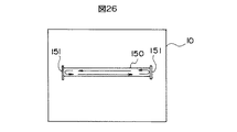
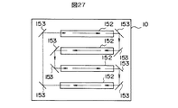
また、本実施の形態では、光導波路14をリング状にすることにより、光信号を循環させているが、光が循環する構造であればリング状以外の光導波路の形状であってもかまわない。例えば、第5の実施の形態として図26に示すように、1本の直線状の光導波路150の両端にミラー151を配置し、伝搬光をミラー151で折り返させ、光導波路150を往復させることにより循環させる構成にすることができる。また、第6の実施の形態として図27に示すように、直線状の光導波路152を平行に配置し、それぞれの端面にミラー153を配置した構成にすることもできる。この図27の構成では、光導波路152の伝搬した光が、端面から出射されて、ミラー153により折り返され、次の光導波路152の端面から入射することを繰り返すことにより、光を循環させる構成である。図26、図27の構成は、光導波路150、152が直線状であるため、光導波路150、151の製造が簡単である。また、図27の構成は、基板10の大きさの割に光導波路152の長さが長くできるため、小さな基板10上に、多数のLSI基板を効率よく配置する必要がある場合に適している。
【0071】
つぎに、本発明の第7の実施の形態のマイクロミラーを備えた光導波路について説明する。
【0072】
第1の実施の形態で示したマイクロミラーを備えた光導波路14では、光導波路14にそって複数のマイクロミラーを配置した場合、ミラーの段数が進むに従って、ミラーによって偏向される光強度が指数関数的に減少してしまうため、多くミラーを配置するためには、光導波路14に入射させる光強度を増やさなければならない。以下、光導波路の上方へ光を偏向することを”跳ね上げ”とも称す。
【0073】
跳ね上げ光強度を増やすためには凸部15の段差高さを高くする方法が考えられるが、これはリソグラフィ工程が煩雑になる欠点がある。
【0074】
そこで、この第7の実施の形態では、伝搬光を基板面の上方に入出射させるために、内部にマイクロミラーを備えた光導波路にあって、マイクロミラーにおける反射光量が一定になるように調製された光導波路を提供する。
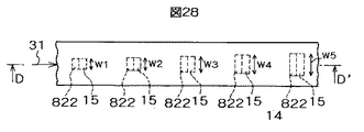
【0075】
図27および図28の構成の光導波路14は、凸部15の光の入射側の斜面にのみアルミ膜822を設けてマイクロミラーを構成している。光導波路14を伝搬する光は、一般に、光導波路14、下部クラッド21、マイクロミラー等の構成部材の材質や、均質度、界面の形状などの影響を受けて吸収あるいは散乱されるため、伝搬光強度は、光導波路内を伝搬するのにともなって減衰する。マイクロミラーが光導波路14中に形成されていない場合には、概ねランバートの吸収則に従って伝搬距離と共に指数関数的に減衰する。マイクロミラーがあることで光信号は一部偏向する。この偏向による伝搬光強度の減衰は、マイクロミラーの面積が大きい程大きくなる。また、図31の様な形状に凸部15を形成した場合、アルミ膜822部分で偏向される他に、凸部15の形状によって伝搬光は一部偏向あるいは散乱する。
【0076】
このように、マイクロミラーを有する光導波路14内を伝搬する光信号の減衰の様子は複雑である。図28で光入射方向31へ伝搬する光信号は、第1のマイクロミラーに到達する時と第2,第3・・・のマイクロミラーに到達する時とでは、順に減衰して到達光量が減少する。そこで、マイクロミラーの面積が全て一定の場合には、それぞれのマイクロミラーで偏向される光量が順に減少することになる。例えば、マイクロミラーで偏向された光信号は、図9に示したように実装された受光素子101を搭載した基板100へ出射されるが、この際、受光素子101の感度以上の光量がマイクロミラーで偏向されることが必須である。そのため、光の入射部から最も遠い位置にあるマイクロミラー、すなわち、最も光信号が減衰して到達したマイクロミラー上に設置された受光素子101に十分な光量を入射させることができるように、当初の光導波路14へ入射させる光量を十分強くしておかねばならない。
【0077】
第7の実施の形態では、各マイクロミラーでの反射光量を一定にするために、それぞれのマイクロミラーに到達する光量の減衰度に応じ反射光量が一定になるように調製する。具体的には、光の入射点に近いマイクロミラーでは、ミラーを小さく、遠くなるにつれてミラーを大きくするようにする。このようにマイクロミラーの大きさが調整されている光導波路の場合には、各マイクロミラーでの反射光量が受光素子の感度以上となるようにすることで、当初光導波路14へ入射させる光量を小さくすることが可能である。従って、例えば、図19に示したような光マルチチップモジュールにこれを適用することにより消費電力を低減することができる。
【0078】
各マイクロミラーでの反射光量を一定にするためには、上述のように到達光量が大きいミラーでは、ミラーの面積を小さくし、到達光量が小さいミラーでは、ミラーの面積を大きくすればよい。マイクロミラー間の距離が等しく設置されておりそれぞれのマイクロミラーが面積以外は同様の構造を持っている場合には、マイクロミラーの面積を等比級数的に大きくしていけば反射光量一定の条件を実現できる。
【0079】
マイクロミラーの面積を等比級数的に変化させるためには、例えば、ミラーの高さを一定として、ミラーの幅を等比級数的(公比=W2/W1=W3/W2=・・・=Wn/Wn−1)に変化させることで実現できる。この場合、ミラーの高さを低くすることが好ましい。ミラーの高さは、光導波路14の高さの5〜20%であることが好ましい。
【0080】
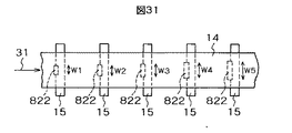
マイクロミラーの面積を等比級数的に変化させるためには、図31の様に凸部15の幅を光導波路14の幅よりも広くして、反射膜であるアルミ膜822の部分の面積だけを変化させることで実現できる。
【0081】
マイクロミラーの面積を等比級数的に変化させるためには、図28の様に凸部15の幅を変化させることで、反射膜の面積を調製することでも実現できる。この構成は、必要な凸部15での光信号の減衰が無いためマイクロミラー部での損失が小さくなり好ましい。このように光導波路14内部にミラーを納める方が望ましい。リソグラフィのマージンを考慮して、コア端部からミラー端部まで2μm以上離すのが好ましい。
【0082】
マイクロミラーを形成するための凸部15の光信号の伝搬方向の長さは、リソグラフィのマージンから5〜200μmが好適である。
【0083】
マイクロミラーの面積を等比級数的に変化させるためには、また、ミラーの幅を一定として、ミラーの高さを等比級数的に変化させることで実現できる。
【0084】
アルミ膜822等の反射膜の光信号の伝搬方向の長さは、2〜20μmが好適である。長すぎるとアルミ膜822が金属クラッディングとして作用する影響で過剰な損失をまねくことになり、短すぎるとリソグラフィが困難となる。
【0085】
光導波路14の寸法は、幅10〜50μm、高さ5〜20μmが好適である。光導波路14の寸法が大きすぎると、モードが増えすぎるため均一な導波光強度が得られなくなる。なお、有機材料、例えばポリイミドを光導波路14の材料に用いることができる。
【0086】
なお、反射光量が一定になるとは、実質的に一定であることを意味する。すなわち、各マイクロミラーではね上げられた光信号が、それぞれのミラー上部に実装された受光素子101に入射する際に、何れの受光素子101においてもその検出感度以下とならず、当初の光導波路14へ入射させる光量を過大としないですむ程度に一定であればよい。
【0087】
また、マイクロミラーを構成する凸部15の傾斜面の形状は、平面、凹面、凸面の何れでも良い。目的に応じて平面、凹面、凸面の形状を選択して用いることにより、集光、拡散等の効果を併せ持たせることができる。
【0088】
マイクロミラーを構成する凸部15の傾斜面の角度は、0〜90°の何れでも良い。また、図28〜図31では上方に偏向する構成を示したが、偏向の方向は、上方、下方、側方の何れでも良い。受光素子、発光素子の設置位置、設置方向などを考慮して決定することができる。
【0089】
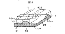
図28、図29のようなマイクロミラーを構成する凸部15を形成する手順を簡単に述べる。まず、平坦な基板上に平坦な下部クラッド21を形成した後、この上に光導波路14と同一の材質の膜を形成し、この膜を等方性エッチング等の方法でテーパー状にエッチングすることで凸部15を形成する。この凸部15上にアルミ膜822を形成した後、光導波路14を形成する。この方法は、特に図31あるいは図32のようにマイクロミラーを構成する凸部15を光導波路14からはみ出すような幅で形成しても、過剰な損失が生じないため好ましい。
【0090】
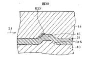
この方法で作成した下部クラッド21の上面は平坦になるが、第1の実施の形態と同様に基板10の表面を凸部形状に加工することにより、下部クラッド21に凸部15を形成する方法にするも可能である。この場合、図30のように、下部クラッド21の上面は平坦にはならない。図30のようなマイクロミラーを有する光導波路14の製造方法についてさらに具体的に説明する。
(1)フォトレジストOFPR−800(東京応化製)をシリコンウエハ基板10に塗布し、90℃で30分オーブンでプリベークした後マスクを介して露光し、現像・リンスを行って凸部15の下部に段差部を形成するためのレジストパターンを得た。段差の間隔は200μmとした。次に濃硝酸/フッ酸混合液(=95/5)を用いて15秒間ウエットエッチングを行った後、濃硫酸/過酸化水素水混合液(=2/1)処理でレジストを剥離し、基板10に段差パターン815(高さ0.5μm)を形成した。
(2)(1)の基板に熱酸化処理(1100℃/6時間、パイロ)を行い、表面に1.2μmの酸化膜(下部クラッド21)を形成した。次にアルミ膜を厚さ0.2μmになるようにスパッタし、段差の側面に架かるように長さ20μm程度にをリソグラフィ処理してアルミ膜822を形成した。このとき、アルミ膜822の幅Wは、最初のミラー幅W1を10μm、n番目のミラーの幅Wnを次式で規定される公比に設定した。
【0091】
公比=W2/W1=Wn+1/Wn
(3)(2)で形成した下部クラッド21上に光導波路14の材料としてOPI−N3505(日立化成製)を塗布・ベークし、ドライエッチングによって、マイクロミラー上にリッジ形状を残して光導波路14(幅40μm×高さ4μm)を形成した。
(4)光導波路14の端部から波長633nmのHe/Neレーザ光を入射し、マイクロミラーにより跳ね上げられた光をCCDカメラで観察し、画像処理によって跳ね上げ光量分布を調べた。ミラー幅が不変である公比=1.0では、跳ね上げ光量が減衰した。等比級数的にミラー幅を増加させていく場合、公比=1.2ではほぼ等しい跳ね上げ光量が得られたのに対し、公比1.3では跳ね上げ光量がnの増加に伴って増大することが確認された。
【0092】
第7の実施の形態の光導波路14においては、入射点に近いところではミラーを小さく、遠くなるにつれて大きくしていくことにより、跳ね上げられる光量の減少を抑えることができる。また、ミラーの大きさを伝搬光量の減少よりも大きくすることにより、跳ね上げ光量を一定量ずつ増やしていくことも容易に可能である。これにより、受光素子101のしきい値以上の光量を跳ね上げることが可能になるため、光導波路14に配置可能なマイクロミラー段数を増やすことができる。
【0093】
上述してきたように、本発明によれば、伝搬光を、基板面の上方に入出射させるために、内部にマイクロミラーを備えた光導波路を容易に製造することのできる製造方法を提供することができる。
【0094】
また、本発明によれば、電気回路と受発光素子とが形成された基板を、光導波路基板上に搭載する構成の光情報処理装置において、電気回路等への電源供給用配線を、導波路基板上に配置することにより、効率よくコンパクトに配置することが可能である。
【0095】
【発明の効果】
以上のように、本発明にかかるマイクロミラーを備えた光導波路の製造方法は、マイクロミラーを備えた光導波路を効率よく製造するのに有用である。また、本発明にかかるマイクロミラーを備えた光導波路は、光情報処理装置の光信号を伝搬する光導波路として有用である。さらに、本発明にかかる光情報処理装置は、情報伝達を光信号で行うことができるため、処理速度の速い情報処理装置として有用である。
【図面の簡単な説明】
【図1】図1は、本発明の第1の実施の形態のマイクロミラーを備えた光導波路を製造する工程を示す断面図である。
【図2】図2は、本発明の第1の実施の形態のマイクロミラーを備えた光導波路を製造する工程を示す断面図である。
【図3】図3は、本発明の第1の実施の形態のマイクロミラーを備えた光導波路を製造する工程を示す断面図である。
【図4】図4は、本発明の第1の実施の形態のマイクロミラーを備えた光導波路を製造する工程を示す断面図である。
【図5】図5は、本発明の第1の実施の形態のマイクロミラーを備えた光導波路を製造する工程を示す断面図である。
【図6】図6は、本発明の第1の実施の形態のマイクロミラーを備えた光導波路を製造する工程を示す断面図である。
【図7】図7は、本発明の第1の実施の形態のマイクロミラーを備えた光導波路を製造する工程を示す断面図である。
【図8】図8は、本発明の第1の実施の形態のマイクロミラーを備えた光導波路を製造する工程を示す断面図である。
【図9】図9は、第1の実施の形態のマイクロミラーを備えた光導波路の伝搬光の入出射を示す説明図である。
【図10】図10は、本発明の第2の実施の形態のマイクロミラーを備えた光導波路を製造する工程を示す断面図である。
【図11】図11は、本発明の第2の実施の形態のマイクロミラーを備えた光導波路を製造する工程を示す断面図である。
【図12】図12は、本発明の第2の実施の形態のマイクロミラーを備えた光導波路を製造する工程を示す断面図である。
【図13】図13は、本発明の第2の実施の形態のマイクロミラーを備えた光導波路を製造する工程を示す断面図である。
【図14】図14は、本発明の第3の実施の形態のマイクロミラーを備えた光導波路を製造する工程を示す断面図である。
【図15】図15は、本発明の第3の実施の形態のマイクロミラーを備えた光導波路を製造する工程を示す断面図である。
【図16】図16は、第3の実施の形態において、マイクロミラーを、光導波路を横切る配線の一部とした場合の光導波路の構成を示す断面図である。
【図17】図17は、図16の光導波路と配線の上面図である。
【図18】図18は、第1〜第3の実施の形態の光導波路に上部クラッドを設け、かつ、光導波路上面を平坦にした構成を示す断面図である。
【図19】図19は、本発明の第4の実施の形態の形態の光情報処理システムの基板10上の光導波路および配線の構成を説明するための上面図である。
【図20】図20は、図19の光情報処理システムにおいて、基板100、111、112に搭載されるLSI、受光素子および発光ダイオードの配置を示すブロック図である。
【図21】図21は、図19の光情報処理システムにおいて、基板10と、基板100等との間の連結構造を示す断面図である。
【図22】図22は、(a),(b),(c) 図19の光情報処理システムにおいて、基板100、111、112上の配線を示すブロック図である。
【図23】図23は、図19の光情報処理システムにおいて、光信号の流れを示す説明図である。
【図24】図24は、図19の光情報処理システムの基板10上の光導波路を製造する工程を示す断面図である。
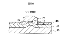
【図25】図25は、図24のC−C’断面図である。
【図26】図26は、本発明の第5の実施の形態の光情報処理システムの光導波路の形状を示す説明図である。
【図27】図27は、本発明の第6の実施の形態の光情報処理システムの光導波路の形状を示す説明図である。
【図28】図28は、本発明の第7の実施の形態のマイクロミラーを備えた光導波路の構成を説明するための上面図である。
【図29】図29は、図28のD−D’断面図である。
【図30】図30は、第7の実施の形態のマイクロミラーを備えた光導波路であって、基板10に段差部815を設けた場合の構成を説明するための断面図である。
【図31】図31は、第7の実施の形態のマイクロミラーを備えた光導波路であって、凸部15の幅を光導波路14の幅よりも大きくした場合の構成を示す上面図である。
【図32】図32は、図31の光導波路14の構成を説明するための斜視図である。
【図33】図33は、図8において、凸部15およびアルミ膜13の幅を光導波路14の幅と同等かそれ以上にした構成を示すための断面図である。[0001]
BACKGROUND OF THE INVENTION
The present invention relates to an optical waveguide used for connecting integrated circuits, a method for manufacturing the same, and an optical information processing apparatus that propagates an optical signal using the optical waveguide.
[0002]
[Prior art]
As a technique of optical interconnection (internal optical coupling) in which an electrical signal is once converted into an optical signal and transmitted / received by an optical signal for transmission / reception of signals between a plurality of integrated circuits, reference Jpn. J. et al. Appl. Phys. Vol. 36 (1997) p. In 1903 to 1906, a configuration for propagating an electrical signal using an optical waveguide on a substrate is disclosed. In this configuration, a light emitting diode and a light receiving element for conversion between an electric signal and an optical signal are attached to an LSI substrate, and this LSI substrate is mounted on a substrate on which an optical waveguide is formed. Then, an optical signal propagating through the optical waveguide is deflected in a direction perpendicular to the substrate surface by a micromirror in the optical waveguide to be emitted from the optical waveguide, and this optical signal is received by a light receiving element on the LSI substrate. In addition, an optical signal is emitted from the light emitting diode toward the optical waveguide, and is deflected in the propagation direction of the optical waveguide by a micromirror in the optical waveguide to propagate through the optical waveguide. As the micromirror in the optical waveguide, a mountain-shaped aluminum mirror formed on the lower surface of the optical waveguide is used. Light is reflected and deflected by the slope of this mountain-shaped aluminum mirror.
[0003]
However, a method for efficiently producing micromirrors in an optical waveguide has not been known conventionally.
[0004]
In addition, when the micromirrors are arranged in multiple stages in the optical waveguide, there is a problem in that the reflected light intensity by the subsequent micromirror decreases due to propagation loss.
[0005]
In the optical interconnection system described above, the input / output signal of the LSI is converted into an optical signal, so that it can be transmitted through the optical waveguide, but it is still necessary to supply the power supply voltage to the LSI, the light emitting diode, and the light receiving element. . For this reason, it becomes a problem where the wiring for supplying the power supply voltage is arranged.
[0006]
[Problems to be solved by the invention]
It is a first object of the present invention to provide a manufacturing method for easily manufacturing an optical waveguide having a micromirror inside to propagate and emit propagating light above a substrate surface.
[0007]
The present invention is an optical waveguide having a multi-stage micromirror inside to propagate and emit the propagating light above the substrate surface, and the optical intensity of the reflected light intensity of the micromirror in the latter stage can be more than a certain level. A second object is to provide a waveguide.
[0008]
The present invention relates to an optical information processing apparatus configured to mount a substrate on which an electric circuit and a light emitting / receiving element are formed on an optical waveguide substrate, and to efficiently and compactly supply power supply wiring to the electric circuit or the like. It is a third object to provide an optical information processing apparatus that can be arranged.
[0009]
[Means for Solving the Problems]
In order to achieve the first object, according to the present invention, the following optical waveguide manufacturing method is provided.
[0010]
That is, a first step of forming on the substrate a clad layer having a convex portion whose side surface is inclined on the surface;
A second step of forming a reflective film on a side surface of the convex portion of the cladding layer;
A third step of forming an optical waveguide on the convex portion of the clad layer, and the first step performs isotropic etching in order to form the convex portion having the inclined side surface. It is a manufacturing method of the optical waveguide provided with the micromirror characterized by using.
[0011]
In order to achieve the second object, according to the present invention, the following optical waveguide is provided.
[0012]
A substrate,
A clad layer having a plurality of convex portions with inclined side surfaces formed on the substrate;
An optical waveguide layer formed on the cladding layer,
An optical waveguide having a reflective film formed on the same side with respect to the light traveling direction of the slopes of the plurality of convex portions,
The reflection film is an optical waveguide characterized in that the amount of reflected light is adjusted according to the attenuation of the amount of light reaching the reflection film.
[0013]
In order to achieve the third object, the present invention provides the following optical information processing apparatus.
[0014]
That is, a waveguide substrate provided with an optical waveguide and a predetermined wiring pattern;
An electric circuit board mounted on the waveguide substrate so as to face the optical waveguide;
Having one or more connecting portions for connecting the waveguide substrate and the electric circuit substrate;
The electric circuit board includes a light receiving element for receiving an optical signal propagating through the optical waveguide, and an electric circuit,
The connecting portion is conductive,
The optical information processing apparatus is characterized in that the wiring pattern is electrically connected to the light receiving element and an electric circuit through the connecting portion.
[0015]
DETAILED DESCRIPTION OF THE INVENTION
An embodiment of the present invention will be described below with reference to the drawings.
[0016]
First, the manufacturing method of the optical waveguide provided with the micromirror of the 1st Embodiment of this invention is demonstrated using FIGS.
[0017]
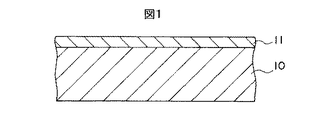
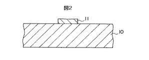
First, as shown in FIG. 1, a
[0018]
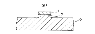
Next, using the resist
[0019]
Thereafter, the resist
[0020]
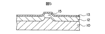
Next, a very thin organic zirconium compound film having a molecular order of thickness is formed on the surface of the lower clad 12. The reason why the coating of the organic zirconium compound is formed in this way is to improve the adhesion strength between the polyimide
[0021]
As shown in FIG. 9, the
[0022]
As described above, in the manufacturing method according to the first embodiment, a convex portion having a slope suitable for a micromirror can be easily formed by using under-etching by isotropic etching. By covering the metal film, the
[0023]
In the present embodiment, the
[0024]
Further, the refractive index of the
[0025]
In the above-described embodiment, the lower clad 12 is formed of an oxide film by thermal oxidation. However, instead of thermal oxidation, an SiO2 film or the like is formed on the
[0026]
Further, in the above-described embodiment, the
[0027]
Further, in the configuration of FIG. 9, power lines and ground lines for supplying drive current to the
[0028]
Next, a method of manufacturing an optical waveguide provided with the micromirror according to the second embodiment of the present invention will be described with reference to FIGS.
[0029]
In this embodiment mode, a micromirror having a slope is formed by isotropic etching of a metal film.
[0030]
First, an SiO2 film is formed on the
[0031]
In this method, since the
[0032]
Further, in this method, since the lower clad 21 is flat, the lower clad 21 can be formed of an organic resin such as polyimide.
[0033]
Furthermore, the manufacturing method of the optical waveguide provided with the micromirror of the 3rd Embodiment of this invention is demonstrated. In this embodiment, a convex portion having an inclined surface is formed on the substrate by using anisotropic etching.
[0034]
The manufacturing method of the third embodiment is almost the same as that of the first embodiment, but a silicon substrate having a (100) plane is used. When such a
[0035]
In this method, since the angle of the (111) plane that is the inclined plane is accurately determined to be 54.7 ° with respect to the (100) plane of the substrate plane, variations in the inclined plane of the micromirror can be eliminated. . Therefore, by designing the mode of the optical waveguide according to the angle of the inclined surface, it is possible to deflect light in a desired direction with high accuracy.
[0036]
Moreover, although the optical waveguide of each of the above-described embodiments has a configuration in which air is used as the upper clad, it may be configured so as to include the upper clad 17 as shown in FIG. As the upper clad 17, an organic resin layer such as a SiO 2 film formed by a sputtering method or a polyimide layer formed by applying and baking OPI-N1005 manufactured by Hitachi Chemical Co., Ltd. can be used.
[0037]
Further, in each of the above-described embodiments, a convex micromirror is formed below the
[0038]
In the first and second embodiments described above, wet etching is used as isotropic etching. However, the present invention is not limited to wet etching, and isotropic etching in which undercut occurs. Dry etching can also be used as long as it can be performed.
[0039]
Next, as a fourth embodiment of the present invention, an optical information processing system configured using the
[0040]
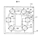
An annular
[0041]
In addition to the
[0042]
On the four
[0043]
A light receiving element is not mounted on the
[0044]
The
[0045]
Similarly, a
[0046]
Further, the
[0047]
Next, the operation of the optical information processing system of this embodiment will be described.
[0048]
The power supply voltage from the
[0049]
By supplying the power supply voltage and the ground voltage, the
[0050]
Since the
[0051]
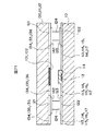
In this embodiment, the
[0052]
Further, the
[0053]
The
[0054]
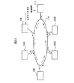
These operations will be specifically described. The
[0055]
When the four optical signals propagate through the optical waveguide and reach the lower part of the
[0056]
Similarly, also in the lower part of the
[0057]
The selection circuit of the
[0058]
As described above, in the optical information processing system of the present embodiment, since the annular
[0059]
In the present embodiment, the
[0060]
In the present embodiment, the supply of the power supply voltage and the like to the
[0061]
Further, by arranging the
[0062]
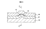
1 to 6 described in the first embodiment, a lower clad is formed on the
[0063]
Next, after a resist film is formed on the lower clad 12, the
[0064]
Next, an OPI coupler manufactured by Hitachi Chemical Co., Ltd. is applied to the surface of the lower clad 12 in the region where the
[0065]
Next, after a
[0066]
This manufacturing method has an advantage that the film forming and lithography processes for manufacturing the
[0067]
In the manufacturing method described above, the
[0068]
In this embodiment, an aluminum film is used to configure the micromirror and the wiring, but it is of course possible to use a film of another metal such as Cr, Cu, Au, or Ag. In addition to the metal film, a dielectric film that reflects propagating light can also be used.
[0069]
In this embodiment, the
[0070]
Further, in this embodiment, the optical signal is circulated by making the
[0071]
Next, an optical waveguide provided with a micromirror according to a seventh embodiment of the present invention will be described.
[0072]
In the
[0073]
In order to increase the jumping light intensity, a method of increasing the step height of the
[0074]
Therefore, in the seventh embodiment, in order to make the propagating light enter and exit above the substrate surface, it is in an optical waveguide provided with a micromirror inside, and is prepared so that the amount of light reflected by the micromirror is constant. An optical waveguide is provided.
[0075]
The
[0076]
Thus, the state of attenuation of the optical signal propagating through the
[0077]
In the seventh embodiment, in order to make the amount of reflected light at each micromirror constant, the amount of reflected light is adjusted to be constant according to the attenuation of the amount of light reaching each micromirror. Specifically, in the micromirror close to the incident point of light, the mirror is made smaller and the mirror is made larger as the distance becomes farther. In the case of an optical waveguide in which the size of the micromirror is adjusted in this way, the amount of light initially incident on the
[0078]
In order to make the amount of light reflected by each micromirror constant, as described above, the mirror area is small for a mirror with a large amount of reaching light, and the mirror area is large for a mirror with a small amount of light. If the distance between the micromirrors is set equal and each micromirror has the same structure except for the area, the condition that the amount of reflected light is constant if the area of the micromirror is increased geometrically Can be realized.
[0079]
In order to change the area of the micromirror in a geometric series, for example, the mirror height is fixed and the width of the mirror is geometrical series (common ratio = W2 / W1 = W3 / W2 =... This can be realized by changing to Wn / Wn-1). In this case, it is preferable to reduce the height of the mirror. The height of the mirror is preferably 5 to 20% of the height of the
[0080]
In order to change the area of the micromirror in a geometric series, the width of the
[0081]
In order to change the area of the micromirror in a geometric series, it can also be realized by adjusting the area of the reflective film by changing the width of the
[0082]
The length of the
[0083]
In order to change the area of the micromirror in a geometric series, it can be realized by changing the height of the mirror in a geometric series while keeping the width of the mirror constant.
[0084]
The length in the propagation direction of the optical signal of the reflective film such as the
[0085]
The dimensions of the
[0086]
In addition, that the amount of reflected light is constant means that it is substantially constant. That is, when the optical signal raised by each micromirror is incident on the
[0087]
Moreover, the shape of the inclined surface of the
[0088]
The angle of the inclined surface of the
[0089]
A procedure for forming the
[0090]
Although the upper surface of the lower clad 21 produced by this method is flat, a method of forming the
(1) Photoresist OFPR-800 (manufactured by Tokyo Ohka Kogyo Co., Ltd.) is applied to the
(2) The substrate of (1) was subjected to thermal oxidation treatment (1100 ° C./6 hours, pyro) to form a 1.2 μm oxide film (lower cladding 21) on the surface. Next, the aluminum film was sputtered to a thickness of 0.2 μm, and an
[0091]
Common ratio = W2 / W1 = Wn + 1 / Wn
(3) OPI-N3505 (manufactured by Hitachi Chemical Co., Ltd.) is applied and baked as a material of the
(4) He / Ne laser light having a wavelength of 633 nm was incident from the end of the
[0092]
In the
[0093]
As described above, according to the present invention, there is provided a manufacturing method capable of easily manufacturing an optical waveguide provided with a micromirror inside in order to cause propagating light to enter and exit above the substrate surface. Can do.
[0094]
According to the present invention, in the optical information processing apparatus configured to mount the substrate on which the electric circuit and the light emitting and receiving elements are formed on the optical waveguide substrate, the power supply wiring to the electric circuit or the like is connected to the waveguide. By arranging on the substrate, it is possible to arrange efficiently and compactly.
[0095]
【The invention's effect】
As described above, the method for manufacturing an optical waveguide provided with a micromirror according to the present invention is useful for efficiently manufacturing an optical waveguide provided with a micromirror. The optical waveguide provided with the micromirror according to the present invention is useful as an optical waveguide for propagating an optical signal of the optical information processing apparatus. Furthermore, the optical information processing apparatus according to the present invention is useful as an information processing apparatus having a high processing speed because it can transmit information using an optical signal.
[Brief description of the drawings]
FIG. 1 is a cross-sectional view showing a process of manufacturing an optical waveguide provided with a micromirror according to a first embodiment of the present invention.
FIG. 2 is a cross-sectional view showing a process of manufacturing an optical waveguide provided with the micromirror according to the first embodiment of the present invention.
FIG. 3 is a cross-sectional view showing a process of manufacturing an optical waveguide provided with the micromirror according to the first embodiment of the present invention.
FIG. 4 is a cross-sectional view showing a process of manufacturing an optical waveguide provided with the micromirror according to the first embodiment of the present invention.
FIG. 5 is a cross-sectional view showing a process of manufacturing an optical waveguide provided with the micromirror according to the first embodiment of the present invention.
FIG. 6 is a cross-sectional view showing a process of manufacturing an optical waveguide provided with the micromirror according to the first embodiment of the present invention.
FIG. 7 is a cross-sectional view showing a process of manufacturing an optical waveguide provided with the micromirror according to the first embodiment of the present invention.
FIG. 8 is a cross-sectional view showing a process of manufacturing an optical waveguide provided with the micromirror according to the first embodiment of the present invention.
FIG. 9 is an explanatory diagram showing incident / exit propagation light of an optical waveguide including the micromirror according to the first embodiment;
FIG. 10 is a cross-sectional view showing a process of manufacturing an optical waveguide provided with a micromirror according to a second embodiment of the present invention.
FIG. 11 is a cross-sectional view showing a process of manufacturing an optical waveguide provided with a micromirror according to a second embodiment of the present invention.
FIG. 12 is a cross-sectional view showing a process of manufacturing an optical waveguide provided with a micromirror according to a second embodiment of the present invention.
FIG. 13 is a cross-sectional view showing a process of manufacturing an optical waveguide provided with a micromirror according to a second embodiment of the present invention.
FIG. 14 is a cross-sectional view showing a process of manufacturing an optical waveguide provided with a micromirror according to a third embodiment of the present invention.
FIG. 15 is a cross-sectional view showing a process of manufacturing an optical waveguide provided with a micromirror according to a third embodiment of the present invention.
FIG. 16 is a cross-sectional view showing a configuration of an optical waveguide when the micromirror is a part of wiring crossing the optical waveguide in the third embodiment.
FIG. 17 is a top view of the optical waveguide and the wiring in FIG. 16;
FIG. 18 is a cross-sectional view showing a configuration in which an upper cladding is provided in the optical waveguides of the first to third embodiments and the upper surface of the optical waveguide is flattened.
FIG. 19 is a top view for explaining a configuration of optical waveguides and wirings on a substrate of an optical information processing system according to a fourth embodiment of this invention.
20 is a block diagram showing an arrangement of LSIs, light receiving elements, and light emitting diodes mounted on
FIG. 21 is a cross-sectional view showing a connection structure between a
22 is a block diagram showing wiring on
FIG. 23 is an explanatory diagram showing the flow of an optical signal in the optical information processing system of FIG. 19;
24 is a cross-sectional view showing a process of manufacturing an optical waveguide on the
FIG. 25 is a cross-sectional view taken along the line CC ′ of FIG.
FIG. 26 is an explanatory diagram showing the shape of an optical waveguide of an optical information processing system according to a fifth embodiment of this invention.
FIG. 27 is an explanatory diagram showing the shape of an optical waveguide of an optical information processing system according to a sixth embodiment of this invention.
FIG. 28 is a top view for explaining a configuration of an optical waveguide including a micromirror according to a seventh embodiment of the present invention.
29 is a cross-sectional view taken along the line DD ′ of FIG. 28. FIG.
FIG. 30 is a cross-sectional view for explaining a configuration in the case where an optical waveguide including a micromirror according to a seventh embodiment and a stepped
FIG. 31 is a top view showing a configuration in the case where an optical waveguide provided with a micromirror according to a seventh embodiment and the width of a
32 is a perspective view for explaining the configuration of the
33 is a cross-sectional view showing a configuration in FIG. 8 in which the widths of the
Claims (5)
Priority Applications (1)
| Application Number | Priority Date | Filing Date | Title |
|---|---|---|---|
| JP2003196759A JP3920249B2 (en) | 1997-10-01 | 2003-07-14 | Optical waveguide |
Applications Claiming Priority (4)
| Application Number | Priority Date | Filing Date | Title |
|---|---|---|---|
| JP26900197 | 1997-10-01 | ||
| JP26900297 | 1997-10-01 | ||
| JP1612298 | 1998-01-28 | ||
| JP2003196759A JP3920249B2 (en) | 1997-10-01 | 2003-07-14 | Optical waveguide |
Related Parent Applications (1)
| Application Number | Title | Priority Date | Filing Date |
|---|---|---|---|
| JP2000-514155A Division JPWO1999017143A1 (en) | 1997-10-01 | 1998-10-01 | Optical waveguide with micromirror, its manufacturing method and optical information processing device |
Publications (2)
| Publication Number | Publication Date |
|---|---|
| JP2004004922A JP2004004922A (en) | 2004-01-08 |
| JP3920249B2 true JP3920249B2 (en) | 2007-05-30 |
Family
ID=30449433
Family Applications (1)
| Application Number | Title | Priority Date | Filing Date |
|---|---|---|---|
| JP2003196759A Expired - Fee Related JP3920249B2 (en) | 1997-10-01 | 2003-07-14 | Optical waveguide |
Country Status (1)
| Country | Link |
|---|---|
| JP (1) | JP3920249B2 (en) |
Families Citing this family (1)
| Publication number | Priority date | Publication date | Assignee | Title |
|---|---|---|---|---|
| JP7622408B2 (en) * | 2020-11-27 | 2025-01-28 | セイコーエプソン株式会社 | Image Processing Device |
-
2003
- 2003-07-14 JP JP2003196759A patent/JP3920249B2/en not_active Expired - Fee Related
Also Published As
| Publication number | Publication date |
|---|---|
| JP2004004922A (en) | 2004-01-08 |
Similar Documents
| Publication | Publication Date | Title |
|---|---|---|
| US7079741B2 (en) | Optical interconnection circuit board and manufacturing method thereof | |
| US20240241329A1 (en) | Heterogeneous packaging integration of photonic and electronic elements | |
| JP4688248B2 (en) | Multilayer optoelectronic substrate having electrical interconnection and optical interconnection and method for manufacturing the same | |
| JP2644303B2 (en) | Fiber optic coupling assembly | |
| CN110998393A (en) | Optical interconnect module with 3D polymer waveguides | |
| JPH0567770A (en) | Optoelectronic integrated circuit device | |
| JP3257776B2 (en) | Optical module mounting structure | |
| KR100463911B1 (en) | Optical information processor | |
| JP3570874B2 (en) | Optical connection structure | |
| JP2003114365A (en) | Optical path conversion device and method of manufacturing the same | |
| KR100460388B1 (en) | Optical waveguide with micromirror, its manufacturing method and optical information processor | |
| JP4624162B2 (en) | Opto-electric wiring board | |
| JP4306011B2 (en) | Optical wiring layer and manufacturing method thereof, optical / electrical wiring substrate, manufacturing method thereof, and mounting substrate | |
| JP3652080B2 (en) | Optical connection structure | |
| JP3920249B2 (en) | Optical waveguide | |
| US7453058B2 (en) | Optical bumps for low-loss interconnection between a device and its supported substrate and related methods | |
| CN111103658A (en) | Device for optical coupling and system for communication | |
| JP2001042171A (en) | Active optical wiring equipment | |
| JP2005148129A (en) | Optical wiring system manufacturing method and optical wiring system | |
| JP2004022666A (en) | Semiconductor device | |
| JP2008102283A (en) | Optical waveguide, optical module, and optical waveguide manufacturing method | |
| JP2001042145A (en) | Opto-electric wiring board | |
| JPWO1999017143A1 (en) | Optical waveguide with micromirror, its manufacturing method and optical information processing device | |
| US20250355198A1 (en) | Optical elements on photonic integrated circuits | |
| JP3886840B2 (en) | Optical path conversion device |
Legal Events
| Date | Code | Title | Description |
|---|---|---|---|
| A621 | Written request for application examination |
Free format text: JAPANESE INTERMEDIATE CODE: A621 Effective date: 20050929 |
|
| RD02 | Notification of acceptance of power of attorney |
Free format text: JAPANESE INTERMEDIATE CODE: A7422 Effective date: 20051220 |
|
| RD03 | Notification of appointment of power of attorney |
Free format text: JAPANESE INTERMEDIATE CODE: A7423 Effective date: 20051220 |
|
| A521 | Written amendment |
Free format text: JAPANESE INTERMEDIATE CODE: A821 Effective date: 20051220 |
|
| A521 | Written amendment |
Free format text: JAPANESE INTERMEDIATE CODE: A523 Effective date: 20060216 |
|
| A521 | Written amendment |
Free format text: JAPANESE INTERMEDIATE CODE: A523 Effective date: 20060216 |
|
| A131 | Notification of reasons for refusal |
Free format text: JAPANESE INTERMEDIATE CODE: A131 Effective date: 20060417 |
|
| A521 | Written amendment |
Free format text: JAPANESE INTERMEDIATE CODE: A523 Effective date: 20060616 |
|
| TRDD | Decision of grant or rejection written | ||
| A01 | Written decision to grant a patent or to grant a registration (utility model) |
Free format text: JAPANESE INTERMEDIATE CODE: A01 Effective date: 20070115 |
|
| A61 | First payment of annual fees (during grant procedure) |
Free format text: JAPANESE INTERMEDIATE CODE: A61 Effective date: 20070214 |
|
| R150 | Certificate of patent or registration of utility model |
Free format text: JAPANESE INTERMEDIATE CODE: R150 |
|
| FPAY | Renewal fee payment (event date is renewal date of database) |
Free format text: PAYMENT UNTIL: 20100223 Year of fee payment: 3 |
|
| FPAY | Renewal fee payment (event date is renewal date of database) |
Free format text: PAYMENT UNTIL: 20110223 Year of fee payment: 4 |
|
| FPAY | Renewal fee payment (event date is renewal date of database) |
Free format text: PAYMENT UNTIL: 20120223 Year of fee payment: 5 |
|
| LAPS | Cancellation because of no payment of annual fees |