JP3916366B2 - Chip thermocompression bonding tool and chip mounting apparatus including the same - Google Patents
Chip thermocompression bonding tool and chip mounting apparatus including the same Download PDFInfo
- Publication number
- JP3916366B2 JP3916366B2 JP2000074710A JP2000074710A JP3916366B2 JP 3916366 B2 JP3916366 B2 JP 3916366B2 JP 2000074710 A JP2000074710 A JP 2000074710A JP 2000074710 A JP2000074710 A JP 2000074710A JP 3916366 B2 JP3916366 B2 JP 3916366B2
- Authority
- JP
- Japan
- Prior art keywords
- ceramic
- indenter
- chip
- holder
- thermocompression bonding
- Prior art date
- Legal status (The legal status is an assumption and is not a legal conclusion. Google has not performed a legal analysis and makes no representation as to the accuracy of the status listed.)
- Expired - Fee Related
Links
Images


Description
【0001】
【発明の属する技術分野】
本発明は、チップ熱圧着ツール及びそれを備えたチップ実装装置に関するものである。
【0002】
【従来の技術】
従来、液晶基板等、各種の基板にチップを熱圧着、すなわち、実装する際に用いられるチップ熱圧着ツールは、各種型式のものが公知である。その一つとして、例えば、特開平7−86341号公報において開示されているように、ツール本体の下端にセラミックホルダーを装着すると共に前記セラミックホルダーの下端にセラミックヒータ及びセラミック圧子を装着したチップ熱圧着ツールが挙げられる。
【0003】
【発明が解決しようとする課題】
ところが、この種のチップ熱圧着ツールは、セラミックホルダーとセラミックヒータとセラミック圧子との一体化(三者相互間の固着)を、適当な接着剤を用いて行っている関係上、接着剤の塗布厚さの不均一性に起因する熱膨張の相違や接着剤の経時的な劣化等によって、或いは、前記接着剤は一般に熱伝導率が小さい為に、これを挟む二者間に発生する温度差に起因する熱変形歪みによって、セラミック圧子の平行度(加工面と基板又は基板保持ステージとの平行度のこと)又は平面度(加工面の平面度のこと)、以下、かかる平行度又は平面度を単に平行度というが、これが経時的に変化し易くて一定しないといった欠点を有していた。
【0004】
加えて、ツール本体が金属製である為、ツール本体とセラミックホルダーとをボルト締めによって固着していたが、この箇所の加熱冷却が繰り返されることに起因してボルト締めに緩みが生じたり、或いは、ツール本体の上端部に装着されている平行度調整機構に熱伝導し、これ等の影響によってもセラミック圧子の平行度が変化し易かった。
【0005】
なお、セラミック圧子の平行度は、特に、ミクロン単位の精度が要求される実装において問題視され、かつ、それが規定内に一定に保たれないと、実装時にチップずれ等が生じて、例えば、それが数μm以下といった高精度の実装が困難になる。
【0006】
そこで、本発明者等は先願(特願平9−282618)において、セラミックホルダーとセラミックヒータとセラミック圧子とを焼結せしめた熱圧着ツールを提案したが、これにおいては、それらの熱膨張及び熱伝導の影響を考慮していない為に、次々と実装して行くうちに、セラミックホルダー等が夫々異なった状態に熱膨張して歪みが発生すると共に、セラミックヒータからの伝熱によってツール本体も加熱されて同様に歪みが発生し、その為、チップ熱圧着ツールの平行度を規定内に一定に保つことが困難になり易く、従って、高精度の実装を一定して行うことの困難性を有していた。本発明は、このような欠点に鑑み、それを解消すべく鋭意検討の結果、得られたものである。
【0007】
【課題を解決するための手段】
すなわち、本発明に係る熱圧着ツールの一つは、請求項1に記載するように、ツール本体の下端に直接若しくはツール本体の下端に装着されている接続ブロックの下端にセラミックホルダーを装着すると共に前記セラミックホルダーの下端に接続孔を有したT字状のセラミックヒータ及びセラミック圧子を焼結せしめたチップ熱圧着ツールにおいて、前記セラミックホルダーの線膨張係数が、前記接続孔を有したT字状のセラミックヒータ及び前記セラミック圧子の線膨張係数と略等しく、かつ、前記セラミック圧子の熱伝導率は、前記接続孔を有したT字状のセラミックヒータから前記セラミック圧子の先端側の加圧面に向うにつれて大きくなり、
前記セラミックホルダーの熱伝導率は、接続孔を有したT字状のセラミックヒータから前記セラミックホルダーの基端側の取付面に向うにつれて小さくなることを特徴とするものである。
【0008】
本発明に係る熱圧着ツールの他の一つは、請求項7に記載するように、ツール本体の下端に直接若しくはツール本体の下端に装着されている接続ブロックの下端にセラミックホルダーを装着すると共に前記セラミックホルダーの下端に接続孔を有したT字状のセラミックヒータ兼用圧子を焼結せしめたチップ熱圧着ツールにおいて、前記セラミックホルダーの線膨張係数が、前記接続孔を有したT字状のセラミックヒータ兼用圧子の線膨張係数と略等しく、かつ、前記セラミックホルダーの熱伝導率は、前記接続孔を有したT字状のセラミックヒータ兼用圧子から前記セラミックホルダーの基端側の取付面に向うにつれて小さくなることを特徴とするものである。
【0009】
また、本発明に係るチップ実装装置は、請求項10に記載するように、請求項1〜9に記載のチップ熱圧着ツールのいずれか一つを備えていることを特徴とするものである。
【0010】
なお、チップ実装装置とは、チップを搭載するマウント装置やチップを接合するボンディング装置に加えて、例えば、基板とチップ、基板と接着剤(ACF、NCF等)など予め対象物同士が接触(搭載又は仮接着等)されたものを加熱加圧することによって固着又は転写させる装置を包含する広い概念の装置をいう。また、基板保持ステージ側は、加熱式、非加熱式のいずれの形態であってもよい。
【0011】
【発明の実施の形態】
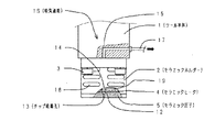
正面図である図1及び図1の左側面図である図2において、チップ熱圧着ツールの下端部分が示されているが、このツールの下端部分は、金属製のツール本体1の下端に直接、セラミックホルダー2(セラミック製のホルダー)が複数のボルト3で固着されていると共に、このホルダー2の下端に、セラミックヒータ4及びセラミック圧子5(セラミック製の圧子)が焼結されている。
【0012】
なお、セラミック圧子5に温度検出手段31(例えば、熱電対、放射温度計など)を設けて設定温度に制御可能な形態に設けられている。
【0013】
すなわち、セラミックヒータ4は、図3において示されているように、発熱部6と端子部7とをT字状に配した所定厚さ(例えば、1mm程度)のパネル体に形成されているが、このヒータ4の発熱部6が、セラミックホルダー2の下端面に形成されている取付け用凹部8に嵌挿されてセラミックホルダー2と焼結されていると共にセラミック圧子5の上端部も、取付け用凹部8に嵌挿されてセラミックホルダー2及びセラミックヒータ4と焼結されている。なお、セラミック圧子5に温度検出手段31(例えば、熱電対、放射温度計など)を装着して設定温度に制御可能に設けている。
【0014】
また、前記焼結は、窒化けい素粉、窒化アルミニウム粉又は窒化ほう素粉等が混入されているバインダーを各部の接触面に塗布した状態で数千気圧下、1700℃〜1800℃に加熱して行うことができ、かつ、これにより、セラミックホルダー2とセラミックヒータ4とセラミック圧子5とを一体化させることができるが、その際、セラミックヒータ4の発熱部6及びセラミック圧子5の上端部が取付け用凹部8に嵌挿されているので、位置ずれを生じさせないで強固に接合することができる。
【0015】
また、セラミックヒータ4は、図3及び図4(発熱部6の縦断面図)において示されているように、電気絶縁材であるセラミック材10で発熱体9を被覆して構成され、その端子部7から発熱体9の端子11を突出せしめていると共に発熱部6に接続孔12を貫通せしめており、そして、この接続孔12は、図1において示されているように、セラミック圧子5に貫通せしめられているチップ吸着孔13とセラミックホルダー2に貫通せしめられている接続孔14とに接続されている。
【0016】
なお、セラミックホルダー2、セラミックヒータ4のセラミック材10及びセラミック圧子5は、窒化けい素に所定量のガラスなどが添加された材で構成され、かつ、セラミックホルダー2の線膨張係数は、セラミックヒータ4及びセラミック圧子5の線膨張係数と同等若しくは略等しく、しかも、それらの熱伝導率は、セラミックヒータ4を基点としてセラミック圧子5の加圧面側(チップ吸着孔13が開口されている面側)へ向う程大きいと共にそれと反対側のセラミックホルダー2の取付面側へ向う程小さくなるように設けている。
【0017】
より具体的には、セラミックホルダー2、セラミックヒータ4及びセラミック圧子5の線膨張係数は、2.5〜3.0(×10-6)/℃であると共に、セラミック圧子5の熱伝導率は、84W/m・K、セラミックホルダー2のそれは、17〜84W/m・Kである。
【0018】
なお、上述のようにセラミックヒータとセラミック圧子とを別体にしないで、それらを一体に構成したセラミックヒータ兼用圧子を装着する場合においては、両者の線膨張係数は、同一又は略同一に設けられると共に熱伝導率は、セラミックホルダー取付部方向へ向う程、小さくなるように設けられる。
【0019】
また、セラミック材は、周知のように、窒化けい素等(主成分)及びガラスなど(添加物)を組成分とするが、ガラスの混入量によって熱伝導率が異なっているので、所定の熱伝導率のものを選択することができる。
【0020】
また、図1においては、接続孔14の上端が示されていないが、接続孔14は、ツール本体1に貫通せしめられている接続孔15に接続されている。このように、接続孔12と14と15とでチップ吸着孔13に連通される吸気通路16を形成している。その為、ツール本体1に装着されている耐圧ホース17を経て吸気することによりチップ吸着孔13から吸気することができ、従って、セラミック圧子5でチップ(図示されていない)を吸着保持することができる。
【0021】
また、セラミックホルダー2に、長穴状の複数の冷却スリット18と第1エアー吹出し通路19と接続孔20(図5参照)とが貫通せしめられているが、第1エアー吹出し通路19は、セラミックヒータ4の発熱部6の上端面上に形成され、かつ、図1において、その左右両端が開口せしめられている。
【0022】
また、接続孔20は、第1エアー吹出し通路19とツール本体1に貫通せしめられている接続孔21(図5参照)とに接続されている。このように、接続孔20と21とで第1エアー吹出し通路19に連通される第1エアー供給通路22を形成している。
【0023】
また、第1エアー供給通路22は、図6において示されているように一対設けられている。その為、ツール本体1に装着されている耐圧ホース23(図5参照)を経てエアーを供給することにより、図1において、第1エアー吹出し通路19の左右両端の開口からエアーを吹き出すことができる。
【0024】
よって、セラミックヒータ4の発熱部6から発せられる熱が、かかるエアーによって奪われ、従って、セラミックヒータ4及びセラミック圧子5を急速に冷却することができると共にセラミックホルダー2に過度に熱伝導するのを防止することができ、しかも、冷却スリット18によって、加熱されたセラミックホルダー2を冷却して、セラミックホルダー2と金属製のツール本体1との接合部が過度に加熱されるのを防止することができる。
【0025】
更に、図2において示されているように、セラミックホルダー2の上端面に一対の第2エアー吹出し通路24が設けられているが、この第2エアー吹出し24は、同図において、前後両端が開口せしめられ、かつ、これに、ツール本体1に貫通せしめられている第2エアー供給通路25が連通せしめられているので、ツール本体1に装着されている耐圧ホース26を経てエアーを供給することにより、図2において、第2エアー吹出し通路24の前後両端の開口からエアーを吹き出すことができて、セラミックホルダー2と金属製のツール本体1との接合部を強制的に冷却することができる。
【0026】
このように、本発明に係るチップ熱圧着ツールの一つは、線膨張率の低い金属製のツール本体1の下端に直接、装着されたセラミックホルダー2とセラミックヒータ4とセラミック圧子5とを焼結すると共に、セラミックホルダー2の線膨張係数は、セラミックヒータ4及びセラミック圧子5の線膨張係数と同等若しくは略等しく、しかも、それらの熱伝導率は、セラミックヒータ4を基点としてセラミック圧子5の加圧面側(チップ吸着孔13が開口されている面側)へ向う程大きいと共にそれと反対側のセラミックホルダー2の取付面側へ向う程小さくなるように設けている。
【0027】
また、セラミックヒータとセラミック圧子とを一体にした形態のセラミックヒータ兼用圧子を装着する場合においては、両者(上側のヒータ部分とその下側の圧子部分)の線膨張係数は、同一又は略同一に設けられると共に熱伝導率は、セラミックホルダー取付部方向へ向う程、小さくなるように設けている。
【0028】
その為、このチップ熱圧着ツールを備えたボンディング装置によって次々と熱圧着(実装)を行っても、セラミック圧子5の平行度を長期間にわたって規定内に保つことがことができ、従って、高精度の実装を一定して行うことができる。
【0029】
図示されていないが、チップ実装装置は、水平面内において移動し得るように装着されている基板保持ステージで液晶基板等の基板を支持すると共に、かかるステージの移動制御若しくは移動回転制御によって基板の実装箇所を、それの上方に装着されているチップ熱圧着ツールが吸着保持しているチップに対して精密に位置合わせせしめ、次いで、チップ吸着孔13を介してチップを吸着保持しているチップ熱圧着ツールを降下させて基板保持ステージ上の前記基板に熱圧着(実装)することができるように構成されている。
【0030】
なお、上記基板保持ステージは、XY方向若しくはXYθ方向に移動制御可能な可動テーブル上に装着されていると共にチップ熱圧着ツールは、水平方向には移動し得ないが、垂直に上下動し得るように装着される。しかし、これ以外の形態に設けてもよい。例えば、チップ熱圧着ツールを回転させ得るように装着したり或いは水平方向へ移動し得るように装着したりしてもよい。
【0031】
また、チップ熱圧着ツールに関し、吸気通路16及びチップ吸着孔13を設けていないものであってもよいが、温度制御の高速応答が図れるので、それらを設ける方が好ましい。また、セラミックホルダー2、セラミックヒータ4及びセラミック圧子5は、アルミナ、ジルコニアのような酸化物系セラミックや、窒化アルミニウム、窒化ほう素、窒化けい素のような非酸化物系セラミックのいずれを用いて構成してもよいが、好ましくは、セラミック圧子5は、前者に比して熱伝導率を調整できる後者が用いられる。
【0032】
また、ツール本体1に対してセラミックホルダー2を、適当な接着剤を用いて固着してもよいが、セラミックヒータ4が損傷した場合等において交換することができるようにボルト締めにより装着するのが好ましく、更には、その他のクランプ機構であってもよい。
【0033】
また、冷却スリット18は、貫通せしめられるのが好ましいが、貫通させないで所定深さに設けてもよく、かつ、その個数は必要に応じて所定個数が選択されると共に、その形状も必要に応じて所定形状に設けられる。
【0034】
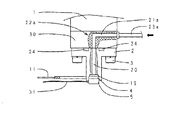
以上、金属製のツール本体1の下端に直接、セラミックホルダー2を装着した場合の形態について述べたが、本発明においては、図7〜9において示されているように、金属製のツール本体1の下端に金属製の接続ブロック30を装着し、そして、この接続ブロック30の下端にセラミックホルダー2を装着すると共にセラミックホルダー2とセラミックヒータ4とセラミック圧子5とを焼結してもよい。
【0035】
なお、図7は正面図、図8,9は図7の左側面図であるが、これらの図において示されているように、接続ブロック30には、吸気通路16aを形成する為の接続孔15aが貫通せしめられていると共に、第2エアー供給通路25a及び第1エアー供給通路22aを形成する為の接続孔21aが貫通せしめられ、そして、第1エアー供給通路22aは、図6において示されている上述の
第1エアー供給通路22と同様に、図9において前後方向に所定間隔に一対設けられ、更に、耐圧ホース17a、23a、26aが装着されている。
【0036】
よって、金属製のツール本体1の下端に接続ブロック30を装着したチップ熱圧着ツールにおいても、金属製のツール本体1の下端に直接、セラミックホルダー2を装着したチップ熱圧着ツールと同様に、セラミックヒータ4の発熱部6からセラミックホルダー2への熱伝導を抑制することができる。
【0037】
従って、セラミックホルダー2の温度昇降の大きさを小さくすることができることにより、歪みが発生しないので、ボルトの緩みも無くなると共に、平行調整機能を有したツール本体の熱膨張による伸び、平行度の狂い(歪み)を無くすることができる。
【0038】
なお、図示されていないが、接続ブロック30は、ボルト締めによって金属製のツール本体1の下端に装着されている。また、セラミック圧子5に、測温用の熱電対31(図2,8参照)が装着されていると共に、ツール本体1は、図示されていないXYZ方向に移動制御可能な可動テーブルを介して三軸方向へ移動し得るように装着されている。
【0039】
しかし、これ以外の、例えば、Z軸方向だけに移動、或いはそれらに加えて所定角度θに回転し得るように装着してもよく、更に、第1,2エアー供給通路22(又は22a),25(又は25a)から第1,2エアー吹出し通路19,24に供給されるエアーについても、常温エアー、冷却エアーのいずれであってもよい。
【0040】
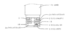
また、セラミックホルダー2に関し、上述のような一体型(図1〜9において示されているような型)に代えて、積層型に設けてもよい。図10,11において、二層型のものが示されているが、このホルダー2は、下側のセラミックブロック2aと上側のセラミックブロック2bとを焼結せしめて形成されている。
【0041】
なお、両ブロック2a,2bは、その熱膨張係数が略同一であるが、その熱伝導率は、上側のセラミックブロック2bの熱伝導率の方が、下側のセラミックブロック2aのそれよりも小さい。このように、二個以上の、すなわち、複数のセラミックブロックをセラミックヒータ側からセラミックホルダー取付部に向って熱伝導率の大きい順に積層して形成(熱伝導率が大きなセラミックブロックの上に、それよりも熱伝導率が小さいセラミックブロックを順に積層して形成)してもよい。
【0042】
このように、セラミックホルダー2を積層型に設けることにより、ホルダー自身及び平行調整機能を有したツール本体1に温度上昇による歪みが発生するのを、より効果的に防止することができ、従って、チップ熱圧着ツールの平行度が短期間で規定外に変化するのを防止することができる。
【0043】
また、上述の図10、11において示されているセラミックブロック2a,2bでは、平面的に積層しているが、凹凸形にして組み合わせた形態であってもよい。更に積層が増えても同様である。
【0044】
すなわち、セラミックホルダー2が、前記一体型(非積層型)及び前記積層型のいずれであっても、セラミックヒータ4部分は高温(例えば、250℃)であると共にツール本体1の下端部分は低温(例えば、30℃〜50℃)である。しかし、前記一体型においては、セラミックホルダー2の中間部分で急激に温度が下がる為に、その温度差による熱変形歪みが発生し易いのに対し、前記積層型においては、そのように熱伝導を妨げる部分がなく急激に温度が下がらず緩やかに下がる故、歪みが発生し難く、従って、これの方が有利である。
【0045】
また、セラミック圧子も、セラミックヒータ側からツール先端側(セラミック圧子の加圧面側)に向って熱伝導率の小さい順にセラミック板を積層し、かつ、線膨張係数を同一又は略同一にすることにより、熱による歪み、伸びの影響を無くすことができる。
【0046】
以上からして明らかのように、本発明に係るチップ熱圧着ツールの構成形態としては、(1)セラミックホルダーとセラミックヒータ兼用圧子との組み合わせと、(2)二層以上のセラミックブロック積層型ホルダーとセラミックヒータ兼用圧子との組み合わせと、(3)セラミックホルダーとセラミックヒータとセラミック圧子との組み合わせと、(4)二層以上のセラミックブロック積層型ホルダーとセラミックヒータとセラミック圧子との組み合わせと、(5)セラミックホルダーとセラミックヒータと二層以上のセラミック板積層型圧子との組み合わせと、(6)二層以上のセラミックブロック積層型ホルダーとセラミックヒータと二層以上のセラミック板積層型圧子との組み合わせ等が挙げられる。
【0047】
なお、セラミックホルダーとセラミックヒータとセラミック圧子との組み合わせ全体の熱伝導率の理想バランスとしては、セラミック圧子の加圧面からセラミックホルダー取付部方向へ向って熱伝導率が小さくなるように設ける方が好ましいが、セラミックヒータは発熱源である為、前記熱伝導率のバランスから外れ出た場合においても本効果は得られ、かつ、かかる本効果は、セラミックホルダー、セラミック圧子夫々を積層型に設けた場合、及び、セラミックホルダーとセラミックヒータとを個別に設けないで、それに代えて、セラミックヒータ兼用圧子を設けても同じである。
【0048】
また、セラミックヒータ及びセラミック圧子は、焼結によって固着せしめる場合のみならず、必要に応じて、取り外し可能な形態に装着、例えば、吸着方法、静電気方法、メカクランプ方法等によって装着してもよい。なお、温度検出手段31はセラミックヒータ4又はセラミックホルダー2に装着してもよいが、チップ吸着位置に最も近い箇所に装着するのが好ましい。
【0049】
また、セラミックホルダー、セラミックヒータ及びセラミック圧子は、基板保持ステージ側に設けることもあるが、この場合、基板保持ステージに装着されたセラミックホルダーの上端にそれらを焼結したり、或いは、取り外し可能な形態に装着、例えば、吸着方法、静電気方法、メカクランプ方法等によって装着したり、更には、重力のみで保持せしめる場合もある。
【0050】
また、本発明におけるチップとは、例えば、半導体チップ、ICチップ、光素子、ウエハなど、その種類や大きさに関係なく、基板に対して搭載又は接合させようとする実装対象物をいう。
【0051】
更に、基板とは、例えば、樹脂基板、ガラス基板、フィルム基板、チップ、ウエハなど、上記チップが搭載又は接合せしめられる方の実装対象物をいう。
【0052】
【発明の効果】
上述のように、本発明によると、セラミックホルダー、セラミックヒータ、セラミック圧子等の省スペース中で、ツール本体とセラミックホルダーの取付部へ熱を伝えにくいように構成したことにより、平行調整機能を有したツール本体の熱膨張による伸び、平行度の狂い(歪み)を無くすることができる。
【0053】
また、セラミックホルダーは、セラミックヒータ側からセラミックホルダ取付部に向って熱伝導を徐々に低下するように焼結により構成し、かつ、線膨張係数を同一又は略同一にするような積層構造にすることにより、隣り合う積層間では温度差を小さくすることができる(急激に熱を落とすのではなく徐々に落とすことができる)為、セラミック圧子、セラミックヒータ、セラミックホルダー、ツール本体の熱変形を押さえることができる。
【0054】
従って、この積層構造により、熱は、チップ加圧側へは伝え易く、平行調整機能を有したツール本体側には伝え難く、線膨張係数は同一又は略同一である為、熱が要因となる問題を無くすことができ、高精度な実装を実現することができる。
【図面の簡単な説明】
【図1】チップ熱圧着ツールの下端部分の正面図である。
【図2】図1の左側面図である。
【図3】セラミックヒータの斜視図である。
【図4】セラミックヒータの発熱部の縦断面図である。
【図5】図1の左側面図である。
【図6】チップ熱圧着ツールの下端部分の正面図である。
【図7】チップ熱圧着ツールの下端部分の正面図である。
【図8】図7の左側面図である。
【図9】図7の左側面図である。
【図10】他の例に係るチップ熱圧着ツールの正面図である。
【図11】図10の左側面図である。
【符号の説明】
1:ツール本体
2:セラミックホルダー
4:セラミックヒータ
5:セラミック圧子
6:発熱部
8:取付け用凹部
13:チップ吸着孔
30:接続ブロック[0001]
BACKGROUND OF THE INVENTION
The present invention relates to a chip thermocompression bonding tool and a chip mounting apparatus including the tool.
[0002]
[Prior art]
Conventionally, various types of chip thermocompression bonding tools used for thermocompression bonding, that is, mounting a chip on various substrates such as a liquid crystal substrate are known. As one of them, for example, as disclosed in JP-A-7-86341, a chip thermocompression bonding in which a ceramic holder is attached to the lower end of the tool body and a ceramic heater and a ceramic indenter are attached to the lower end of the ceramic holder. Tools.
[0003]
[Problems to be solved by the invention]
However, in this type of chip thermocompression bonding tool, the ceramic holder, ceramic heater and ceramic indenter are integrated (adherence between the three) using a suitable adhesive. Due to differences in thermal expansion due to thickness non-uniformity, deterioration of the adhesive over time, etc., or because the adhesive generally has a low thermal conductivity, the temperature difference generated between the two sandwiching it Due to thermal deformation strain caused by the above, the parallelism of the ceramic indenter (the parallelism between the processed surface and the substrate or the substrate holding stage) or the flatness (the flatness of the processed surface). Is simply referred to as parallelism, but it has a drawback that it is easy to change over time and is not constant.
[0004]
In addition, since the tool main body is made of metal, the tool main body and the ceramic holder are fixed by bolting, but the bolting is loosened due to repeated heating and cooling of this part, or The parallelism of the ceramic indenter easily changed due to the heat conduction to the parallelism adjusting mechanism mounted on the upper end of the tool body.
[0005]
In addition, the parallelism of the ceramic indenter is regarded as a problem particularly in mounting where accuracy in units of microns is required, and if it is not kept constant within the specification, chip deviation or the like occurs during mounting, for example, It becomes difficult to mount with high accuracy of several μm or less.
[0006]
In view of this, the present inventors have proposed a thermocompression bonding tool in which a ceramic holder, a ceramic heater, and a ceramic indenter are sintered in a prior application (Japanese Patent Application No. 9-282618). Since the effect of heat conduction is not taken into consideration, the ceramic holders etc. will thermally expand to different states and become distorted as they are mounted one after the other, and the tool body will also be affected by heat transfer from the ceramic heater. Similarly, distortion occurs when heated, so it is difficult to keep the parallelism of the chip thermocompression bonding tool constant within the specified range. Therefore, it is difficult to perform high-precision mounting constantly. Had. The present invention has been obtained as a result of intensive studies in order to eliminate such drawbacks.
[0007]
[Means for Solving the Problems]
That is, according to one of the thermocompression bonding tools according to the present invention, as described in
The thermal conductivity of the ceramic holder decreases from the T-shaped ceramic heater having a connection hole toward the mounting surface on the base end side of the ceramic holder .
[0008]
As another aspect of the thermocompression bonding tool according to the present invention, as described in
[0009]
In addition, a chip mounting apparatus according to the present invention includes any one of the chip thermocompression bonding tools according to
[0010]
In addition to the mounting device for mounting the chip and the bonding device for bonding the chip, the chip mounting device is such that, for example, the substrate and the chip, the substrate and the adhesive (ACF, NCF, etc.) contact each other in advance (mounting). Or a device having a broad concept including a device for fixing or transferring by heat-pressing what has been temporarily bonded or the like. Further, the substrate holding stage side may be either a heating type or a non-heating type.
[0011]
DETAILED DESCRIPTION OF THE INVENTION
In FIG. 1 which is a front view and FIG. 2 which is a left side view of FIG. 1, the lower end portion of the chip thermocompression bonding tool is shown. The lower end portion of this tool is directly connected to the lower end of the
[0012]
The
[0013]
That is, as shown in FIG. 3, the
[0014]
The sintering is performed by heating at 1700 ° C. to 1800 ° C. under several thousand atmospheres with a binder mixed with silicon nitride powder, aluminum nitride powder, boron nitride powder or the like applied to the contact surface of each part. In this case, the
[0015]
Further, as shown in FIGS. 3 and 4 (longitudinal sectional view of the heat generating portion 6), the
[0016]
The
[0017]
More specifically, the linear expansion coefficient of the
[0018]
In the case where the ceramic heater combined with the ceramic heater and the ceramic indenter are mounted separately as described above, the linear expansion coefficient of the both is set to be the same or substantially the same. At the same time, the thermal conductivity is provided so as to decrease toward the ceramic holder mounting portion.
[0019]
In addition, as is well known, ceramic materials have silicon nitride or the like (main component) and glass or the like (additives) as components, but the thermal conductivity differs depending on the amount of glass mixed in. One having conductivity can be selected.
[0020]
Although the upper end of the
[0021]
The
[0022]
Further, the
[0023]
A pair of the first
[0024]
Therefore, the heat generated from the heat generating portion 6 of the
[0025]
Further, as shown in FIG. 2, a pair of second
[0026]
As described above, one of the chip thermocompression bonding tools according to the present invention bakes the
[0027]
When a ceramic heater / indenter in which the ceramic heater and the ceramic indenter are integrated is mounted, the linear expansion coefficients of both (the upper heater portion and the lower indenter portion) are the same or substantially the same. In addition to being provided, the thermal conductivity is provided so as to decrease toward the ceramic holder mounting portion.
[0028]
For this reason, the parallelism of the
[0029]
Although not shown, the chip mounting apparatus supports a substrate such as a liquid crystal substrate on a substrate holding stage mounted so as to be movable in a horizontal plane, and mounts the substrate by controlling the movement or rotation of the stage. The chip is precisely positioned with respect to the chip held by the chip thermocompression bonding tool mounted above it, and then the chip thermocompression bonding that holds the chip through the
[0030]
The substrate holding stage is mounted on a movable table whose movement can be controlled in the XY direction or XYθ direction, and the chip thermocompression bonding tool cannot move in the horizontal direction, but can move up and down vertically. It is attached to. However, it may be provided in other forms. For example, the chip thermocompression bonding tool may be mounted so as to be rotated or mounted so as to be moved in the horizontal direction.
[0031]
In addition, the chip thermocompression bonding tool may not be provided with the
[0032]
Further, the
[0033]
The cooling slit 18 is preferably penetrated, but may be provided at a predetermined depth without penetrating, and the predetermined number is selected as necessary, and the shape thereof is also required. Are provided in a predetermined shape.
[0034]
As mentioned above, although the form at the time of attaching the
[0035]
7 is a front view, and FIGS. 8 and 9 are left side views of FIG. 7. As shown in these drawings, the
[0036]
Therefore, in the chip thermocompression bonding tool in which the
[0037]
Accordingly, since the magnitude of the temperature rise and fall of the
[0038]
Although not shown, the
[0039]
However, other than this, for example, it may be mounted so that it can move only in the Z-axis direction, or can be rotated to a predetermined angle θ in addition thereto, and further, the first and second air supply passages 22 (or 22a), The air supplied from 25 (or 25a) to the first and second
[0040]
Moreover, regarding the
[0041]
Both the blocks 2a and 2b have substantially the same thermal expansion coefficient, but the thermal conductivity of the upper ceramic block 2b is smaller than that of the lower ceramic block 2a. . In this way, two or more ceramic blocks, that is, a plurality of ceramic blocks are laminated from the ceramic heater side to the ceramic holder mounting portion in order of increasing thermal conductivity (on the ceramic block having high thermal conductivity, Alternatively, ceramic blocks having lower thermal conductivity may be stacked in order.
[0042]
In this way, by providing the
[0043]
Further, although the ceramic blocks 2a and 2b shown in FIGS. 10 and 11 are laminated in a plane, they may be combined in an uneven shape. The same applies even if the number of layers increases.
[0044]
That is, regardless of whether the
[0045]
The ceramic indenter is also formed by laminating ceramic plates in ascending order of thermal conductivity from the ceramic heater side to the tool tip side (pressure surface side of the ceramic indenter), and by making the linear expansion coefficient the same or substantially the same. The effect of strain and elongation due to heat can be eliminated.
[0046]
As can be seen from the above, the configuration of the chip thermocompression bonding tool according to the present invention includes (1) a combination of a ceramic holder and a ceramic heater combined indenter, and (2) a ceramic block multi-layer holder having two or more layers. And (3) a combination of a ceramic holder, a ceramic heater and a ceramic indenter, and (4) a combination of a ceramic block laminate type holder of two or more layers, a ceramic heater and a ceramic indenter ( 5) Combination of ceramic holder, ceramic heater and two or more layers of ceramic plate stacking indenter; (6) Combination of two or more layers of ceramic block stacking type holder, ceramic heater and two or more layers of ceramic plate stacking indenter Etc.
[0047]
In addition, as an ideal balance of the thermal conductivity of the entire combination of the ceramic holder, the ceramic heater, and the ceramic indenter, it is preferable to provide the thermal conductivity to decrease from the pressing surface of the ceramic indenter toward the ceramic holder mounting portion. However, since the ceramic heater is a heat generation source, this effect can be obtained even when the thermal conductivity is out of balance, and this effect can be obtained when the ceramic holder and the ceramic indenter are provided in a laminated type. In addition, the ceramic holder and the ceramic heater are not separately provided, and a ceramic heater combined indenter is provided instead.
[0048]
Further, the ceramic heater and the ceramic indenter may be mounted not only in the case of being fixed by sintering but also in a removable form, for example, by an adsorption method, an electrostatic method, a mechanical clamp method, or the like, if necessary. The
[0049]
The ceramic holder, ceramic heater and ceramic indenter may be provided on the substrate holding stage side. In this case, they can be sintered or removed from the upper end of the ceramic holder mounted on the substrate holding stage. It may be attached to the form, for example, attached by an adsorption method, an electrostatic method, a mechanical clamp method, or may be held only by gravity.
[0050]
In addition, the chip in the present invention refers to an object to be mounted or bonded to a substrate, for example, a semiconductor chip, an IC chip, an optical element, a wafer or the like regardless of the type or size.
[0051]
Furthermore, the substrate refers to a mounting object on which the chip is mounted or bonded, such as a resin substrate, a glass substrate, a film substrate, a chip, or a wafer.
[0052]
【The invention's effect】
As described above, according to the present invention, a parallel adjustment function is provided by configuring the ceramic holder, ceramic heater, ceramic indenter, and the like so that heat is not easily transmitted to the mounting portion of the tool body and the ceramic holder. Elongation due to thermal expansion of the tool body and parallelism deviation (distortion) can be eliminated.
[0053]
The ceramic holder is constructed by sintering so that the heat conduction gradually decreases from the ceramic heater side toward the ceramic holder mounting portion, and has a laminated structure in which the linear expansion coefficients are the same or substantially the same. As a result, the temperature difference between adjacent stacks can be reduced (it can be gradually reduced rather than suddenly dropping heat), so that the thermal deformation of the ceramic indenter, ceramic heater, ceramic holder and tool body is suppressed. be able to.
[0054]
Thus, this laminated structure, heat is easily transmitted in the chip pressure side, rather flame reportedly on the tool body side having a parallel adjustment function, since the coefficient of linear expansion the same or substantially the same, the heat is a factor Problems can be eliminated and high-precision mounting can be realized.
[Brief description of the drawings]
FIG. 1 is a front view of a lower end portion of a chip thermocompression bonding tool.
FIG. 2 is a left side view of FIG.
FIG. 3 is a perspective view of a ceramic heater.
FIG. 4 is a longitudinal sectional view of a heat generating part of a ceramic heater.
FIG. 5 is a left side view of FIG. 1;
FIG. 6 is a front view of a lower end portion of a chip thermocompression bonding tool.
FIG. 7 is a front view of a lower end portion of a chip thermocompression bonding tool.
8 is a left side view of FIG.
9 is a left side view of FIG.
FIG. 10 is a front view of a chip thermocompression bonding tool according to another example.
11 is a left side view of FIG.
[Explanation of symbols]
1: Tool body 2: Ceramic holder 4: Ceramic heater 5: Ceramic indenter 6: Heat generating part 8: Recess for mounting 13: Chip suction hole 30: Connection block
Claims (10)
前記セラミックホルダーの熱伝導率は、接続孔を有したT字状のセラミックヒータから前記セラミックホルダーの基端側の取付面に向うにつれて小さくなることを特徴とするチップ熱圧着ツール。A ceramic holder is attached directly to the lower end of the tool body or to the lower end of a connection block attached to the lower end of the tool body, and a T-shaped ceramic heater and ceramic indenter having a connection hole at the lower end of the ceramic holder are sintered. In the crimped chip thermocompression bonding tool, the linear expansion coefficient of the ceramic holder is substantially equal to the linear expansion coefficient of the T-shaped ceramic heater having the connection hole and the ceramic indenter, and the thermal conductivity of the ceramic indenter Increases from the T-shaped ceramic heater having the connection hole toward the pressure surface on the tip side of the ceramic indenter,
The chip thermocompression bonding tool, wherein the thermal conductivity of the ceramic holder decreases from a T-shaped ceramic heater having a connection hole toward a mounting surface on the base end side of the ceramic holder .
Priority Applications (1)
| Application Number | Priority Date | Filing Date | Title |
|---|---|---|---|
| JP2000074710A JP3916366B2 (en) | 1999-03-16 | 2000-03-16 | Chip thermocompression bonding tool and chip mounting apparatus including the same |
Applications Claiming Priority (3)
| Application Number | Priority Date | Filing Date | Title |
|---|---|---|---|
| JP11-70229 | 1999-03-16 | ||
| JP7022999 | 1999-03-16 | ||
| JP2000074710A JP3916366B2 (en) | 1999-03-16 | 2000-03-16 | Chip thermocompression bonding tool and chip mounting apparatus including the same |
Publications (3)
| Publication Number | Publication Date |
|---|---|
| JP2000332061A JP2000332061A (en) | 2000-11-30 |
| JP2000332061A5 JP2000332061A5 (en) | 2005-07-07 |
| JP3916366B2 true JP3916366B2 (en) | 2007-05-16 |
Family
ID=26411400
Family Applications (1)
| Application Number | Title | Priority Date | Filing Date |
|---|---|---|---|
| JP2000074710A Expired - Fee Related JP3916366B2 (en) | 1999-03-16 | 2000-03-16 | Chip thermocompression bonding tool and chip mounting apparatus including the same |
Country Status (1)
| Country | Link |
|---|---|
| JP (1) | JP3916366B2 (en) |
Families Citing this family (7)
| Publication number | Priority date | Publication date | Assignee | Title |
|---|---|---|---|---|
| WO2002041385A1 (en) * | 1999-03-16 | 2002-05-23 | Toray Engineering Co., Ltd. | Tool for thermo-compression-bonding chips, and chip packaging device having the same |
| US6821381B1 (en) | 1999-03-16 | 2004-11-23 | Toray Engineering Co., Ltd. | Tool for thermo-compression-bonding chips, and chip packaging device having the same |
| AT414079B (en) * | 2002-12-20 | 2006-08-15 | Datacon Semiconductor Equip | DEVICE FOR POSITIONING |
| AT412603B (en) * | 2003-03-12 | 2005-04-25 | Datacon Semiconductor Equip | DEVICE FOR CONNECTING ELECTRONIC CIRCUITS |
| JP4941305B2 (en) | 2005-10-12 | 2012-05-30 | 株式会社村田製作所 | Joining device |
| JP6106320B2 (en) * | 2016-06-24 | 2017-03-29 | 東レエンジニアリング株式会社 | Mounting device |
| CN115394689B (en) * | 2022-09-05 | 2023-09-01 | 江苏富乐华功率半导体研究院有限公司 | Hot-pressing sintering device for power semiconductor device |
-
2000
- 2000-03-16 JP JP2000074710A patent/JP3916366B2/en not_active Expired - Fee Related
Also Published As
| Publication number | Publication date |
|---|---|
| JP2000332061A (en) | 2000-11-30 |
Similar Documents
| Publication | Publication Date | Title |
|---|---|---|
| JP4941305B2 (en) | Joining device | |
| JP4749072B2 (en) | Wafer holder | |
| US20060021705A1 (en) | Substrate mounting apparatus and control method of substrate temperature | |
| TWI681478B (en) | Installation device and installation method | |
| US6821381B1 (en) | Tool for thermo-compression-bonding chips, and chip packaging device having the same | |
| JP3916366B2 (en) | Chip thermocompression bonding tool and chip mounting apparatus including the same | |
| JP2018060833A (en) | Electrostatic chuck and substrate fixing device | |
| CN106068061B (en) | Electronic component engaging head | |
| KR20190001271A (en) | Bonding head and apparatus for bonding chips having the bonding head | |
| KR20200067322A (en) | Bonding head and apparatus for bonding chips having the bonding head | |
| JP7164959B2 (en) | HOLDING DEVICE AND HOLDING DEVICE MANUFACTURING METHOD | |
| CN111212489A (en) | Heater assembly | |
| JP5552826B2 (en) | Substrate laminating apparatus, laminated semiconductor device manufacturing method, and laminated semiconductor device | |
| JP3872568B2 (en) | Chip thermocompression tool | |
| WO2002041385A1 (en) | Tool for thermo-compression-bonding chips, and chip packaging device having the same | |
| JP3898630B2 (en) | Press heating device | |
| JP7352317B2 (en) | Bonding equipment and bonding head adjustment method | |
| WO2022211370A1 (en) | Bonding tool having high flatness and provided with polycrystalline diamond tip integrated with cemented carbide body | |
| KR102658985B1 (en) | Bonding head and die bonding apparatus including the same | |
| KR101614252B1 (en) | Unit for preheating a printed circuit board and apparatus for bonding a die including the same | |
| JP3123354U (en) | Heater device for semiconductor wafer | |
| KR101578605B1 (en) | Unit for preheating a printed circuit board and apparatus for bonding a die including the same | |
| JP4089966B2 (en) | Press heater and processing method thereof | |
| JP2024019807A (en) | holding device | |
| JP2001332588A (en) | Scrub head for mounting chip |
Legal Events
| Date | Code | Title | Description |
|---|---|---|---|
| A621 | Written request for application examination |
Free format text: JAPANESE INTERMEDIATE CODE: A621 Effective date: 20040402 |
|
| A521 | Written amendment |
Free format text: JAPANESE INTERMEDIATE CODE: A523 Effective date: 20041028 |
|
| A871 | Explanation of circumstances concerning accelerated examination |
Free format text: JAPANESE INTERMEDIATE CODE: A871 Effective date: 20041028 |
|
| A975 | Report on accelerated examination |
Free format text: JAPANESE INTERMEDIATE CODE: A971005 Effective date: 20041122 |
|
| A977 | Report on retrieval |
Free format text: JAPANESE INTERMEDIATE CODE: A971007 Effective date: 20041208 |
|
| A131 | Notification of reasons for refusal |
Free format text: JAPANESE INTERMEDIATE CODE: A131 Effective date: 20041214 |
|
| A521 | Written amendment |
Free format text: JAPANESE INTERMEDIATE CODE: A523 Effective date: 20050209 |
|
| A02 | Decision of refusal |
Free format text: JAPANESE INTERMEDIATE CODE: A02 Effective date: 20050303 |
|
| RD02 | Notification of acceptance of power of attorney |
Free format text: JAPANESE INTERMEDIATE CODE: A7422 Effective date: 20050404 |
|
| A521 | Written amendment |
Free format text: JAPANESE INTERMEDIATE CODE: A523 Effective date: 20050428 |
|
| A911 | Transfer of reconsideration by examiner before appeal (zenchi) |
Free format text: JAPANESE INTERMEDIATE CODE: A911 Effective date: 20050512 |
|
| A912 | Removal of reconsideration by examiner before appeal (zenchi) |
Free format text: JAPANESE INTERMEDIATE CODE: A912 Effective date: 20050603 |
|
| A521 | Written amendment |
Free format text: JAPANESE INTERMEDIATE CODE: A523 Effective date: 20061208 |
|
| A521 | Written amendment |
Free format text: JAPANESE INTERMEDIATE CODE: A523 Effective date: 20061226 |
|
| A61 | First payment of annual fees (during grant procedure) |
Free format text: JAPANESE INTERMEDIATE CODE: A61 Effective date: 20070206 |
|
| R150 | Certificate of patent or registration of utility model |
Free format text: JAPANESE INTERMEDIATE CODE: R150 |
|
| FPAY | Renewal fee payment (event date is renewal date of database) |
Free format text: PAYMENT UNTIL: 20100216 Year of fee payment: 3 |
|
| FPAY | Renewal fee payment (event date is renewal date of database) |
Free format text: PAYMENT UNTIL: 20110216 Year of fee payment: 4 |
|
| FPAY | Renewal fee payment (event date is renewal date of database) |
Free format text: PAYMENT UNTIL: 20120216 Year of fee payment: 5 |
|
| FPAY | Renewal fee payment (event date is renewal date of database) |
Free format text: PAYMENT UNTIL: 20120216 Year of fee payment: 5 |
|
| FPAY | Renewal fee payment (event date is renewal date of database) |
Free format text: PAYMENT UNTIL: 20130216 Year of fee payment: 6 |
|
| FPAY | Renewal fee payment (event date is renewal date of database) |
Free format text: PAYMENT UNTIL: 20140216 Year of fee payment: 7 |
|
| LAPS | Cancellation because of no payment of annual fees |