JP3904018B2 - Microsample processing observation method and apparatus - Google Patents
Microsample processing observation method and apparatus Download PDFInfo
- Publication number
- JP3904018B2 JP3904018B2 JP2005107006A JP2005107006A JP3904018B2 JP 3904018 B2 JP3904018 B2 JP 3904018B2 JP 2005107006 A JP2005107006 A JP 2005107006A JP 2005107006 A JP2005107006 A JP 2005107006A JP 3904018 B2 JP3904018 B2 JP 3904018B2
- Authority
- JP
- Japan
- Prior art keywords
- sample
- micro
- stage
- sample stage
- processing
- Prior art date
- Legal status (The legal status is an assumption and is not a legal conclusion. Google has not performed a legal analysis and makes no representation as to the accuracy of the status listed.)
- Expired - Lifetime
Links
Images


Description
本発明は、被観察対象物の表面のみならず表面に近い内部の断面をも観察分析すること
を必要とする、半導体デバイス,液晶デバイス,磁気ヘッド、等の電子デバイスやマイク
ロデバイス等の研究開発や製造における観察・分析・評価手段として利用される装置シス
テムに関する。
The present invention researches and develops electronic devices such as semiconductor devices, liquid crystal devices, magnetic heads, and micro devices that require observation and analysis of not only the surface of the object to be observed but also the internal cross section close to the surface. The present invention relates to an apparatus system used as an observation / analysis / evaluation means in manufacturing and manufacturing.
ダイナミックランダムアクセスメモリに代表される半導体メモリやマイクロプロセッサ
,半導体レーザなど半導体デバイス、および磁気ヘッドなど電子部品の製造においては、
製品の品質管理のために製造工程途中あるいは終了の段階で製品特性が検査される。検査
では、製作寸法の計測や、回路パターンの欠陥検査や異物分析がなされる。このため、各
種の手段が用意され利用されている。
In the manufacture of semiconductor devices such as dynamic random access memory, semiconductor devices such as microprocessors and semiconductor lasers, and electronic components such as magnetic heads,
Product characteristics are inspected during or during the manufacturing process for product quality control. In the inspection, measurement of manufacturing dimensions, inspection of circuit pattern defects, and analysis of foreign matter are performed. For this reason, various means are prepared and used.
特に異常箇所が製品の内部に存在する場合は、従来、集束イオンビーム(Focused Ion
beam : FIB)装置と電子顕微鏡を組み合わせた、微細加工観察装置が用いられる機会
が増している。この装置は特許文献1に開示されている。
In particular, when there is an abnormal part inside the product, the conventional focused ion beam (Focused Ion
Beam: FIB) An opportunity to use a microfabrication observation apparatus combining an electron microscope and an electron microscope is increasing. This apparatus is disclosed in
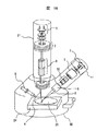
同種の装置の概略構成を、図16を用いて説明する。走査電子顕微鏡機能を有する集束
イオンビーム装置は、真空試料室60を有しており、イオン源1,イオンビーム走査偏向
器3、およびレンズ2などから構成される集束イオンビーム光学系31,FIB照射によ
って試料から放出する二次電子や二次イオンを検出する二次粒子検出器6,半導体ウェー
ハや半導体チップなどのウェーハ21を載置する試料台24などが配置されている。また
、電子ビームを放出する電子銃7,電子ビームレンズ9,電子ビーム走査偏向器10、な
どから構成される走査電子顕微鏡光学系41を設置している。
A schematic configuration of the same type of apparatus will be described with reference to FIG. A focused ion beam apparatus having a scanning electron microscope function has a
次に、本装置の動作について説明する。まず、イオン源1から放出したイオンを、レン
ズ31を通してウェーハ21に照射する。FIB4は試料上で直径数ナノメートルから1
マイクロメートル程度に細束化される。FIB4をウェーハ21に照射するとスパッタリ
ング現象により試料表面の構成原子が真空中に放出される。したがってイオンビーム走査
偏向器3を用いてFIB4を走査させることで、マイクロメートルからサブマイクロメー
トルレベルの加工ができることになる。そこで、図14において試料となるウェーハ21
を装置内部の試料台24に載せ、座標値で指定された観察箇所p1を位置出し後、観察箇
所にFIB4を照射し溝穴を掘り、図15に示す観察箇所の内部断面s1を創生する。創
生された溝穴の外面や内壁面を、電子ビーム照射による走査電子顕微鏡機能で観察したり
、分析装置51で適宜分析する。尚、ウェーハプロセスで用いられる従来の微細加工観察
装置は、集束イオンビーム光学系と電子ビーム光学系を、試料表面の観察部位で両ビーム
軸が交差する様に配置されている。
Next, the operation of this apparatus will be described. First, the ions emitted from the
It is bundled to about a micrometer. When the FIB 4 is irradiated onto the
Is placed on the
ところで最近、観察部位を含むミクロンオーダーの微小領域を切出した微小試料を加工
観察装置の外部へ取り出し、別途用意した装置に微小試料を移して最適形状に追加工し観
察・分析する方法が考案され利用されている。この方法は、特許文献2に開示されている
。
Recently, a method has been devised in which a micro-sample cut out of a micron-order region including the observation site is taken out of the processing observation device, transferred to a separately prepared device, and further processed into an optimal shape for observation and analysis. It's being used. This method is disclosed in
この方法は図17に示すように、まず、試料102の表面に対しFIB4が直角に照射
するように試料102の姿勢を保ち、試料上でFIB4を矩形に走査させ、試料表面に所
要の深さの角穴107を形成する(図17(a))。次に、試料102を傾斜させ、底穴
108を形成する。試料102の傾斜角の変更は、試料台(図示せず)によって行われる
(図17(b))。試料102の姿勢を変更し、試料102の表面がFIB4に対して再
び垂直になるように試料102を設置し、切り欠き溝109を形成する(図17(c))
。マニピュレータ(図示せず)を駆動し、マニピュレータ先端のプローブ72の先端を、
試料102を分離する部分に接触させる(図17(d))。ガスノズル110から堆積性ガ
ス105を供給し、FIB4をプローブ72の先端部を含む領域に局所的に照射し、イオ
ンビームアシストデポジション膜(以下、デポ膜104と略す)を形成する。接触状態に
ある試料102の分離部分とプローブ72の先端はデポ膜104で接続される(図17
(e))。FIB4で残りの部分を切り欠き加工し(図17(f))、試料102から分離試
料である微小試料12を切出す。切出された分離試料12は、接続されたプローブ72で
支持された状態になる(図17(g))。この微小試料12を、FIB4で加工し、観察
しようとする領域をウォール加工するとTEM試料(図示せず)となる。以上がウェーハ
などの試料から所望の解析領域を含む微小試料を、FIB加工と微小試料の搬送手段を駆
使して分離する方法である。この方法で分離した微小試料を本微細加工装置の外に取り出
し、各種観察・分析装置に導入することで解析することができる。但し、試料を大気に晒
すことを嫌う場合には利用できない。また、別装置も必要になるため設備コストや設置ス
ペースの増加することが避けられない。
In this method, as shown in FIG. 17, first, the posture of the
. A manipulator (not shown) is driven, and the tip of the
The
(E)). The remaining part is cut out with FIB 4 (FIG. 17 (f)), and a
以上述べた従来法には次のような問題がある。 The conventional methods described above have the following problems.
問題(1)FIB加工で形成した試料の穴溝断面を観察するには、試料台を傾斜させる
ことにより斜め方向から穴溝内壁断面を観察する。その場合、FIB装置のワーキングデ
ィスタンスや、対物レンズの存在、或るいは試料台の大きさに起因する構造上の制約によ
り試料台の傾斜角度調整範囲が、制限され、それ以上の角度に傾斜できない。従って溝内
壁断面の垂直観察は不可能である。しかしながら半導体デバイス製造のプロセス開発等に
おけるドライエッチング,平坦化,薄膜形成等の処理特性確認では垂直断面観察が不可欠
であるが、上記公知例の装置では対応できなかった。
Problem (1) In order to observe the hole groove cross section of the sample formed by FIB processing, the hole groove inner wall cross section is observed from an oblique direction by inclining the sample stage. In this case, the tilt angle adjustment range of the sample stage is limited due to the structural distance caused by the working distance of the FIB apparatus, the presence of the objective lens, or the size of the sample stage, and the tilt cannot be increased beyond that. . Accordingly, vertical observation of the groove inner wall cross section is impossible. However, vertical cross-section observation is indispensable for confirmation of processing characteristics such as dry etching, flattening, and thin film formation in the process development of semiconductor device manufacturing, etc., but the apparatus of the above-mentioned known example cannot cope with it.
問題(2)斜め観察による分解能低下が大きな問題になる。ウェーハ表面に対し斜め上
方から電子ビームを照射し穴溝内壁断面を観察する場合、ウェーハ表面に垂直方向即ち溝
穴内壁断面の観察分解能が低下する。低下率は、およそ30°では約15%、最も多用さ
れる45°近辺では30%にも達する。最近の半導体デバイスの微細化は極限に達してお
り、数ナノメータ以下の精度での寸法や形状の測定が必要となっている。要求される観察
分解能は3nm以下と、走査電子顕微鏡の技術的限界域に突入している。加えてこの程度
の高分解能下では焦点深度が極めて浅くなり1μmの数10%以下の範囲しかピントが合
わないため、斜め観察時のデバイス縦方向断面の適正観察範囲は、要求領域の半分にも満
たない場合が頻発する。この問題は垂直観察することにより全観察領域で焦点の合った高
品位な観察が可能にできる。
Problem (2) Decrease in resolution due to oblique observation is a major problem. When irradiating the wafer surface with an electron beam obliquely from above and observing the cross section of the inner wall of the hole groove, the observation resolution in the direction perpendicular to the wafer surface, that is, the inner wall section of the groove hole is lowered. The reduction rate is about 15% at about 30 °, and reaches 30% at around 45 °, which is most frequently used. Recent miniaturization of semiconductor devices has reached the limit, and it is necessary to measure dimensions and shapes with an accuracy of several nanometers or less. The required observation resolution is 3 nm or less, which has entered the technical limit of the scanning electron microscope. In addition, under such a high resolution, the depth of focus becomes extremely shallow and only a range of several tens of percent of 1 μm is in focus. Therefore, the proper observation range of the device longitudinal section during oblique observation is half the required area. Less often occurs. This problem can be achieved by performing high-speed observation with focus in the entire observation region by performing vertical observation.
問題(3)観察断面がウェーハ上に形成した微小な溝穴壁面に存在するため、穴から出
てくる二次電子の数密度がウェーハ表面と比較して減少する。従って二次電子検出効率が
低下することで二次電子像のS/Nの低下を招き、断面観察の精度低下を余儀なくされた
。
Problem (3) Since the observed cross section exists on the wall surface of the minute slot formed on the wafer, the number density of secondary electrons coming out of the hole is reduced as compared with the wafer surface. Therefore, the secondary electron detection efficiency is lowered, leading to a reduction in the S / N of the secondary electron image, and the accuracy of cross-sectional observation is inevitably lowered.
LSIパターンの微細化は止まることなく2〜3年毎に30%低減するペースで進んで
おり、観察装置には益々高い分解能が要求されている。更には電子ビームを照射して励起
される原子特性X線の面分布をX線検出器で測定して元素分析(EDX分析)を行っても、
試料中への電子ビーム侵入によるX線発生領域の拡大により、電子ビーム径が0.1μm
以下であっても、分析の面分解能は約1μmとなってしまい、微細な構造を持つLSI素
子断面の分析には不十分であった。
The miniaturization of LSI patterns is steadily progressing at a pace of 30% reduction every 2 to 3 years, and higher resolution is required for observation devices. Furthermore, even if elemental analysis (EDX analysis) is performed by measuring the surface distribution of atomic characteristic X-rays excited by irradiation with an electron beam with an X-ray detector,
Due to the expansion of the X-ray generation area due to the penetration of the electron beam into the sample, the electron beam diameter becomes 0.1 μm
Even in the following cases, the surface resolution of the analysis is about 1 μm, which is insufficient for analyzing the cross-section of the LSI element having a fine structure.
問題(4)断面垂直観察が不可欠とされる事例として、ウェーハプロセスにおけるエッ
チング加工,溝穴埋め込み,平坦化加工等の出来栄え評価が挙げられる。加工断面の寸法
や形状を正確に測定するために、従来はウェーハから見たい断面を含むチップサイズの試
料を割り出し、汎用の走査電子顕微鏡などで観察している。ところがデバイスの微細化進
展やウェーハの大口径化に伴い、素子回路パターンの観察したい位置で正確に破断する作
業が非常に難しいため失敗も出ている。一方、評価用ウェーハの供給能力不足や価格上昇
のため評価試料作成の失敗が許されない状況にある。
Problem (4) As an example in which cross-sectional vertical observation is indispensable, there are performance evaluations such as etching processing, groove hole embedding, and planarization processing in a wafer process. In order to accurately measure the dimension and shape of a processed cross section, conventionally, a chip size sample including a cross section to be viewed from a wafer is determined and observed with a general-purpose scanning electron microscope or the like. However, with the progress of miniaturization of devices and the increase in diameter of wafers, the work of accurately breaking at the position where the element circuit pattern is desired to be observed is very difficult, and there have been failures. On the other hand, due to insufficient supply capacity of evaluation wafers and price increases, evaluation sample preparation is not allowed to fail.
問題(5)特許文献2に開示された手法では観察・分析の精度は分解能など十分な水準
を確保できるが、試料を従来装置内で製作し、これを装置外部に取りだし、別に用意した
観察・分析装置に導入する必要があるため、微小試料の取り出しから加工・観察・分析ま
での所要時間が数時間にも及ぶ問題があった。加えて、試料を大気に暴露すると酸化や吸
湿等で劣化するケースでは、その回避が困難であった。半導体デバイスの断面観察は、最
近では半導体製造時の有益な検査手法として重視されつつあり、その場合の処理能力は現
時点で毎時2〜3ヶ所以上の観察・分析が望まれており、今後さらなる高速処理が要望さ
れる動向にある。この要望に対して従来法の処理能力は極端に低いという問題が解決され
ていない。
Problem (5) Although the method disclosed in
上述の問題点に鑑み、本願の目的は、対象試料の内部断面を垂直断面観察できて、高分
解能,高精度,高スループット,大気暴露による劣化無し、失敗無しに観察・分析できる
微小試料加工観察装置および微小試料加工観察方法を提供することにある。
In view of the above-mentioned problems, the purpose of this application is to observe the internal cross-section of the target sample in a vertical cross-section, with high resolution, high accuracy, high throughput, no degradation due to atmospheric exposure, and observation / analysis without failure An object of the present invention is to provide an apparatus and a micro sample processing observation method.
以上に述べたような目的は、以下のようにすることによって達成される。 The object as described above is achieved by the following.
(1)イオン源,イオンビームを集束するレンズ,イオンビーム走査偏向器、を備える
集束イオンビーム光学系と、電子源,電子ビームを集束するレンズ,電子ビーム走査偏向
器、を備える電子ビーム光学系と、荷電粒子を試料に照射して該試料からの二次粒子を検
出する検出器と、該試料を併せ持つ試料台を備える微小試料加工観察装置において、集束
イオンビームを用いて該試料から微小試料を分離する機能と、該微小試料を摘出するため
のマニピュレータを具備し摘出された該微小試料を前記電子ビームまたは前記集束イオン
ビームで観察する機能を有することを特徴とする微小試料加工観察装置とする。これによ
り、対象試料の内部断面を二次電子の収率を高くして観察できるため高分解能観察ができ
、しかも微小試料を装置の外部に取り出すことが無いため短時間で観察・分析できる微小
試料加工観察装置を提供できる。
(1) An electron beam optical system including a focused ion beam optical system including an ion source, a lens for focusing an ion beam, and an ion beam scanning deflector, and an electron source, a lens for focusing the electron beam, and an electron beam scanning deflector. And a micro sample processing and observation apparatus comprising a detector for irradiating a sample with charged particles to detect secondary particles from the sample, and a sample stage having the sample together. And a micro sample processing and observation apparatus comprising a manipulator for extracting the micro sample and observing the extracted micro sample with the electron beam or the focused ion beam To do. This makes it possible to observe the internal cross-section of the target sample with a high yield of secondary electrons, enabling high-resolution observation, and the micro sample can be observed and analyzed in a short time because it is not taken out of the device. A processing observation apparatus can be provided.
(2)該マニピュレータには該試料から摘出した該微小試料の位置と姿勢を調節する機
能を有することを特徴とする請求項1記載の微小試料加工観察装置とする。
(2) The micro sample processing and observation apparatus according to
これにより、微小試料を走査電子顕微光学系もしくは集束イオンビーム光学系に対し位
置を移動できるため、観察分解能がより高くなる位置に微小試料を配置することができる
。また微小試料の内部断面観察方向を選択することができる。このため断面を垂直に観察
すれば、二次電子の収率も高いことから、高分解能で観察できる微小試料加工観察装置を
提供できる。
As a result, the position of the micro sample can be moved relative to the scanning electron microscope optical system or the focused ion beam optical system, so that the micro sample can be arranged at a position where the observation resolution becomes higher. In addition, the direction of observing the internal cross section of the micro sample can be selected. For this reason, if the cross section is observed vertically, the yield of secondary electrons is also high, so that a micro sample processing observation apparatus that can observe with high resolution can be provided.
(3)微小試料の位置と姿勢を調節する機能が、荷電粒子ビームの該微小試料への照射
角度可変機能を含むことを特徴とする請求項2記載の微小試料加工観察装置とする。
(3) The micro sample processing and observation apparatus according to
これにより、対象試料の内部断面観察方向を自由に選択することができる。このため断
面を垂直に観察すれば、エッチングや平坦化の形状寸法や埋め込み状況,膜厚等を高分解
能で観察でき、高精度な計測・評価ができる微小試料加工観察装置を提供できる。
Thereby, the internal cross-section observation direction of the target sample can be freely selected. For this reason, if the cross section is observed vertically, it is possible to provide a minute sample processing observation apparatus capable of observing with high resolution the shape dimension, embedding condition, film thickness, etc. of etching and flattening, with high accuracy.
(4)試料から分離した該微小試料に接続するマニピュレータと、該マニピュレータを
駆動させるマニピュレータ制御装置と、該試料台と独立に駆動して荷電粒子ビームの該微
小試料への照射角度可変機能を有する第2の試料台を具備することを特徴とする請求項2
記載の微小試料加工観察装置とする。これにより、対象試料の内部断面を高分解能かつ短
時間で観察・分析できる微小試料加工観察装置を提供できる。また、第2の試料台に固定
した微小試料をマニピュレータから切り離して、1つのマニピュレータで複数の微小試料
を第2の試料台に固定することが可能となることで、断面観察と元素解析の時間を短縮す
ることができる。またマニピュレータから切り離して微小試料を第2の試料台に固定する
ことで、導入試料を保持する試料台の防振機構と微小試料を固定する第2の試料台の防振
機構を共有することができる。
(4) A manipulator connected to the micro sample separated from the sample, a manipulator control device for driving the manipulator, and a function of changing the irradiation angle of the charged particle beam to the micro sample by driving independently of the sample stage The second sample stage is provided.
The described micro sample processing and observation apparatus. Thereby, it is possible to provide a micro sample processing and observation apparatus capable of observing and analyzing the internal cross section of the target sample with high resolution and in a short time. In addition, it is possible to separate the micro sample fixed to the second sample stage from the manipulator and fix a plurality of micro samples to the second sample stage with one manipulator, so that time for cross-sectional observation and elemental analysis can be obtained. Can be shortened. Further, by separating the micro sample from the manipulator and fixing it to the second sample stage, it is possible to share the anti-vibration mechanism of the sample stage that holds the introduced sample and the anti-vibration mechanism of the second sample stage that fixes the micro sample. it can.
(5)導入試料から分離した該微小試料に接続するマニピュレータと、該マニピュレー
タを該試料台と独立に駆動させるマニピュレータ制御装置とを具備し、該微小試料を前記
マニピュレータで支持した状態で、観察用荷電粒子ビームの該微小試料への照射角度可変
機能を有することを特徴とする請求項2記載の微小試料加工観察装置とする。これにより
、対象試料の内部断面を高分解能かつ短時間で観察・分析できる微小試料加工観察装置を
提供できる。また、該微小試料を固定する第2の試料台を必要としないために、微小試料
断面観察のための操作が簡単になり、操作時間を短くできる。
(5) A manipulator connected to the micro sample separated from the introduced sample, and a manipulator control device for driving the manipulator independently from the sample stage, with the micro sample supported by the manipulator for
(6)荷電粒子ビーム照射時に該微小試料から発生するX線を検出するX線検出器を備
えることを特徴とする請求項1から5記載の微小試料加工観察装置とする。これにより、
対象試料の内部断面を高分解能かつ短時間で観察・分析できる微小試料加工観察装置を提
供できる。また、荷電粒子線照射時の原子特性X線検出による元素分析において、微小試
料を薄膜化することで、荷電粒子線の試料への侵入によるX線発生領域拡大を回避できる
ので高分解能元素分析が可能となる。
(6) An apparatus for processing and observing a micro sample according to any one of
It is possible to provide a micro sample processing and observation apparatus capable of observing and analyzing an internal cross section of a target sample with high resolution and in a short time. In elemental analysis based on atomic characteristic X-ray detection at the time of charged particle beam irradiation, it is possible to avoid the expansion of the X-ray generation area due to penetration of the charged particle beam into the sample by thinning the micro sample. It becomes possible.
(7)集束イオンビーム光学系を具備し、且つ、試料に対する該光学系の傾斜角度を可
変する機構を有することを特徴とする請求項1記載の該微小試料加工観察装置とする。こ
れにより、対象試料の内部断面を高分解能かつ短時間で観察・分析できる微小試料加工観
察装置を提供する。特に、該光学系の傾斜角度を可変できるため多様な試料作製方法およ
び試料形状を実現できる。
(7) The micro-sample processing and observation apparatus according to
(8)集束イオンビーム光学系を2基具備することを特徴とする請求項1記載の該微小
試料加工観察装置とする。これにより、対象試料の内部断面を高分解能かつ短時間で観察
・分析できる微小試料加工観察装置を提供する。特に、2基の集束イオンビーム光学系を
用いるため、短時間の試料作製が可能になる。また、試料台を傾斜しない構造とすれば装
置の小型化も可能になる。
(8) The micro-sample processing and observation apparatus according to
(9)微小試料を全自動で切出す機能を有することを特徴とする微小試料加工観察装置
とする。これにより、対象試料の内部断面を高分解能かつ短時間で観察・分析できる微小
試料加工観察装置を提供する。特に装置操作の自動化により操作者の負担を軽減できるの
で、より短時間の観察・分析が可能となる。
(9) A micro sample processing and observation apparatus having a function of cutting out a micro sample fully automatically. This provides a micro sample processing and observation apparatus capable of observing and analyzing the internal cross section of the target sample with high resolution and in a short time. In particular, since the burden on the operator can be reduced by automating the operation of the apparatus, it is possible to observe and analyze in a shorter time.
(10)真空装置内で、集束イオンビームを用いて比較的大形な導入試料の表面から観
察対象部位を微小試料として分離し、該微小試料を、マニピュレータを駆動して導入試料
から摘出し、該微小試料を、真空雰囲気の試料室内に置いたまま、電子ビームまたは集束
イオビームで該微小試料の特定部位を観察することを特徴とする微小試料加工観察方法と
する。これにより、対象試料の内部断面を二次電子の収率を高くして観察できるため高分
解能観察ができ、かつ微小試料を装置の外部に取り出すことが無いため短時間で観察・分
析できる微小試料加工観察方法を提供できる。
(10) In a vacuum apparatus, a focused ion beam is used to separate the observation target site from the surface of the relatively large introduced sample as a minute sample, and the minute sample is removed from the introduced sample by driving a manipulator; A method for processing and observing a micro sample is characterized by observing a specific portion of the micro sample with an electron beam or a focused ion beam while the micro sample is placed in a sample chamber in a vacuum atmosphere. This makes it possible to observe the internal cross-section of the target sample with a high yield of secondary electrons, enabling high-resolution observation, and removing the micro sample outside the device, so that the micro sample can be observed and analyzed in a short time A processing observation method can be provided.
(11)前記微小試料の形状は四面体または五面体であることを特徴とする微小試料加
工観察方法とする。これにより、対象試料の内部断面を高分解能かつ短時間で観察・分析
できる微小試料加工観察方法を提供する。特に、微小試料を分離するのに加工に無駄が少
ないため短時間で微小試料作製ができる。
(11) The microsample processing and observation method is characterized in that the shape of the microsample is a tetrahedron or a pentahedron. This provides a micro sample processing and observation method capable of observing and analyzing the internal cross section of the target sample with high resolution and in a short time. In particular, since there is little waste in processing to separate a micro sample, the micro sample can be manufactured in a short time.
(12)前記導入試料はパターン無し或いはパターン付きの半導体ウェーハであること
を特徴とする微小試料加工観察方法とする。これにより、対象試料の内部断面を高分解能
かつ短時間で観察・分析できる微小試料加工観察方法を提供する。特に、半導体ウェーハ
に適用することにより、半導体製造プロセス検査に活用でき、デバイス不良の早期発見お
よび短時間品質管理により製造歩留まりの向上に貢献する。
(12) The micro sample processing and observation method is characterized in that the introduced sample is a semiconductor wafer having no pattern or a pattern. This provides a micro sample processing and observation method capable of observing and analyzing the internal cross section of the target sample with high resolution and in a short time. In particular, by applying it to semiconductor wafers, it can be used for semiconductor manufacturing process inspection, and contributes to the improvement of manufacturing yield by early detection of device defects and short-time quality control.
本発明により、益々微細化が進むLSIデバイス等の内部観察を高分解能で高品質かつ
短時間で実施できる微小試料加工観察装置および微小試料加工観察方法が実現できる。さ
らに薄膜成形加工した微小試料をEDX分析して高精度な元素分析することにより、総合
的に断面の観察や分析の効率の良い微小試料加工観察装置を提供できる。
According to the present invention, it is possible to realize a micro sample processing and observation apparatus and a micro sample processing and observation method capable of performing internal observation of LSI devices and the like that are increasingly miniaturized with high resolution and high quality in a short time. Furthermore, by performing EDX analysis of a micro sample formed by thin film processing and performing high-precision elemental analysis, it is possible to provide a micro sample processing / observing apparatus with a comprehensive cross-section observation and analysis efficiency.
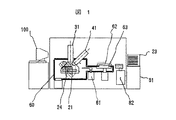
本発明の実施形態である微小試料加工観察装置の構成及びその動作を説明する。
(実施例1)
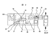
第1の実施例の装置構成と動作を図1,図2および図3を用いて説明する。図1,図2
は装置全体構成を、図3は集束イオビーム光学系、走査電子顕微鏡光学系および試料台周
辺の構成を詳細に示す。なお、本実施の形態では、本発明の微小試料加工観察装置のうち
ウェーハ対応装置を示す。また、図3は、図1の概略俯瞰断面を表しているが、説明の都
合上、機器の向きや詳細には幾分の相違があるが本質的差ではない。図1において、装置
システムの中心部には集束イオンビーム光学系31と電子ビーム光学系41が真空試料室
60の上部に適宜設置されている。真空試料室60の内部には試料となるウェーハ21を
載置する試料台24が設置されている。2基の光学系31及び41は各々の中心軸がウェ
ーハ21表面付近で一点に交わるように調整されている。試料台24にはウェーハ21を
前後左右に高精度で移動する機構を内蔵しており、ウェーハ21上の指定箇所が集束イオ
ンビーム光学系31の真下に来るように制御される。試料台24は回転,上下、あるいは
傾斜する機能を有する。真空試料室60には図示を省略した排気装置が接続され適切な圧
力に制御されている。尚、光学系31,41にも図示を省略した排気系を個別に備え適切
な圧力に維持している。真空試料室60内にはウェーハ導入手段61,ウェーハ搬送手段
62を有する。真空試料室60に隣接してウェーハ移載ロボット82,カセット導入手段
81が配置されている。真空試料室60の左隣には装置全体及び試料加工観察評価の一連
の処理を制御管理する操作制御部100を配備している。
A configuration and operation of a micro sample processing and observation apparatus according to an embodiment of the present invention will be described.
Example 1
The apparatus configuration and operation of the first embodiment will be described with reference to FIGS. 1 and 2
3 shows the overall configuration of the apparatus, and FIG. 3 shows the configuration of the focused ion beam optical system, the scanning electron microscope optical system, and the periphery of the sample stage in detail. In the present embodiment, a wafer handling apparatus is shown among the micro sample processing and observation apparatus of the present invention. FIG. 3 shows a schematic overhead cross-section of FIG. 1, but there are some differences in the orientation and details of the device for convenience of explanation, but this is not an essential difference. In FIG. 1, a focused ion beam
次に、本実施形態のウェーハ導入操作を概説する。ウェーハカセット23がカセット導
入手段81のテーブルに置かれ、作業開始指令が操作制御卓100から発せられると、ウ
ェーハ搬送ロボット82がカセット内の指定されたスロットから試料となるウェーハを引
き出し、図2に示すオリエンテーション調整手段83でウェーハ21の向きを所定の位置
に調整される。次いで、ウェーハ21はウェーハ搬送ロボット82によりウェーハ導入手
段61上部のハッチ62が開かれた時点でウェーハを載置台63に乗せられる。ハッチ
62を閉じると、ウェーハ周囲に狭い空間が形成されロードロック室となり、図示を省略
した真空排気手段で排気した後、載置台63を下降する。次いで、ウェーハ搬送手段61
が載置台63のウェーハ21を取り上げ、真空試料室60中央の試料台24に載置する。
尚、試料台24にはウェーハ21の反り矯正や振動防止のためウェーハ21をチャックす
る手段を必要に応じて設ける。ウェーハ21上の観察分析位置p1の座標値を操作制御部
100から入力して、試料台24を動かしウェーハ21の観察分析位置p1を集束イオン
ビーム光学系31の直下に合わせて停止する。
Next, the wafer introduction operation of this embodiment will be outlined. When the
Picks up the
The
次に、図3を用いて試料加工観察評価の過程を説明する。本発明の微小試料加工観察装
置では、集束イオビーム光学系31は、イオン源1,イオン源1から放出するイオンビー
ムを集束するレンズ2,イオンビーム走査偏向器3等で構成され、また、電子ビーム光学
系41は、電子銃7,前記電子銃7から放出する電子ビーム8を集束する電子レンズ9,
電子ビーム走査偏向器10で構成される。その他に、集束イオンビーム(FIB)4また
は電子ビーム8をウェーハ21に照射してウェーハからの二次粒子を検出するための二次
粒子検出器6,ウェーハ21を載せる可動の試料台24,所望の試料位置を特定するため
試料台の位置を制御する試料台制御装置25,プローブ72の先端を微小試料の摘出位置
に移動し、摘出し、集束イオンビーム(FIB)4または電子ビーム8を照射して微小試
料の特定位置を観察評価する上で最適な位置や方向を制御するためのマニピュレータ制御
装置15と電子ビーム8の照射時に励起される原子特性X線検出のためのX線検出器16
と、堆積ガス供給装置17を備えている。
Next, the process of sample processing observation evaluation will be described with reference to FIG. In the micro sample processing and observation apparatus of the present invention, the focused ion beam
It comprises an electron
And a deposition
次に、本実施形態で、ウェーハ導入後の試料加工観察評価の過程を概説する。まず、試
料台を下げてプローブ72の先端をウェーハ21から離した状態で、試料台24に対して
水平方向(XY方向)にプローブ72を移動し、プローブ72の先端をFIB4の走査領
域に設定する。マニピュレータ制御装置15は位置座標を保存した後、プローブ72を退
避する。
Next, in this embodiment, the process of sample processing observation evaluation after wafer introduction will be outlined. First, in a state where the sample stage is lowered and the tip of the
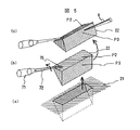
集束イオンビーム光学系31からFIB4をウェーハ21に照射して、図4に示すよう
に観察分析位置p2を横切ってコの字を描くように溝を形成する。加工領域は、長さ約5
μm,幅約1μm,深さ約3μmであり、片方側面でウェーハ21と接続している。その
後、試料台24を傾斜させ、FIB4で三角柱の斜面を形成するように加工する。ただし
、この状態では、微小試料22とウェーハ21とは支持部で接続されている。
The FIB 4 is irradiated onto the
It is μm, width is about 1 μm, depth is about 3 μm, and is connected to the
次に、試料台24傾斜を戻した後、微小試料22に、マニピュレータ70先端のプロー
ブ72を微小試料22の端部に接触させた後に、FIB4の照射により堆積性ガスを接触
点75に堆積させてプローブ72を微小試料22に接合し一体化する。更に、支持部S2
をFIB4で切断して微小試料22を切取る。微小試料22はプローブ72に支持された
状態になり、観察・分析を目的とする表面及び内部断面が微小試料22の観察分析面p3
として取り出す準備が完了する。
Next, after returning the inclination of the sample table 24, the
Is cut with the FIB 4 to cut out the
Ready to take out as
次に、図5の(b)に示すように、マニピュレータ70を操作して微小試料22をウェ
ーハ21表面から浮上する高さまで持ち上げる。尚、必要に応じてプローブ72に支持さ
れた状態で微小試料22にFIB4の照射角をマニピュレータの回転操作で適切に追加工
して所望の観察断面p3を形成する。この追加工の一例としてFIB4が持つビームのテ
ーパによって斜めに形成された観察断面p2を真に垂直断面とするための仕上げ加工があ
る。これまで行われてきた断面加工/観察ではFIBで掘った穴の側壁を観察面としなけ
ればならなかったのに対し、本実施例装置によれば、持ち上げた後に追加工することが可
能であり、観察対象面を適宜移動させつつ、対加工を行うことができるので、所望の断面
を適正に形成することが可能になる。
Next, as shown in FIG. 5B, the
次に、微小試料22を回転させて、電子ビーム光学系41の電子ビーム8が観察断面
p3へ概略垂直に入射するようにマニピュレータ70を動かして微小試料22の姿勢を制
御した後静止させる。これにより、二次粒子検出器6での二次電子の検出効率は、試料断
面を観察する場合であっても、ウェーハ最表面を観察する場合と同程度になり、微小試料
22の観察分析面p3の観察条件は非常に良好なものになり、従来例で問題であった分解
能の低下を回避でき、しかも観察分析面p2,p3の角度を望ましい角度に調整できるの
で、より綿密な観察分析ができるようになる。
Next, the
また、微小試料22を、装置の外部に取り出すことなく、真空雰囲気の試料室内に置い
たまま、観察・分析するため、対象試料の内部断面を室内大気暴露による汚染や異物付着
無しに、高分解能,高精度,最適角度での観察・分析が実現可能となる。しかも1時間当
たり2〜3ヶ所以上の高い処理能力での観察・分析が可能となる。
In addition, since the
更に、本実施例装置では観察断面p3を持つ微小試料22を、マニュピュレータ70に
よって種々の傾斜や移動を行うことができるので、例えば観察断面p2に孔を設け、試料
内部の3次元的な断層形成状態をも確認することが可能になる。
Furthermore, since the
なお、図3の例ではFIB4を挟んで対向して、マニュピュレータ70と電子ビーム光
学系41が形成されているが、マニピュレータ70等の動作数を減らして加工/観察時間
を極力減らすためは、マニピュレータ70と電子ビーム光学系41間の相対角度が、FIB4
の照射方向に対し垂直な面内で、90°に近い角度となるように形成されることが望まし
い。なぜならこのように形成することによって、マニピュレータ70は、ウェーハ21か
ら微小試料22を持ち上げる動作、電子ビーム8に対し観察断面p2が垂直となるように
プローブ72を回転させる動作、及びその他の微調動作のみを行えば良いからである。
In the example of FIG. 3, the
It is desirable to form an angle close to 90 ° in a plane perpendicular to the irradiation direction. Because of this formation, the
また、上記説明ではウェーハ21からマニピュレータ70によって、微小試料22を持
ち上げる例を用いているが、これに限られることはなくウェーハ21を降下させることに
より、結果的に微小試料22を持ち上げるようにしても良い。この場合、試料台24には
ウェーハ21をZ方向(FIB4の光軸方向)に移動させるZ軸移動機構を設けておく。
このような構成によれば、ウェーハ21内の微小試料22となる個所に、電子ビーム光学
系41の光軸を位置づけた状態で微小試料22の切出しと持ち上げを行うことが可能にな
る。この場合、FIB4による微小試料22の切出しから、観察断面p2の観察に至るま
での工程を電子顕微鏡で確認しつつ実行でき、かつその間の照射位置の変更をあまり行う
ことなく実現することが可能になる。
In the above description, an example in which the
According to such a configuration, it is possible to cut out and lift the
なお電子ビーム光学系41によって、ウェーハ21の表面を斜めから見た電子顕微鏡像
が得られるが、この電子顕微鏡像に、加工予定断面やFIB4による加工到達位置を重畳
しモデル表示すれば、FIB4による断面加工状態を容易に確認することができる。加工
予定断面を電子顕微鏡像に重畳表示するには、設定される加工深さと、倍率から算出され
る電子顕微鏡像内の寸法に基づいて、断面となる部分を示すアニメーションを電子顕微鏡
に重畳表示する。
The electron beam
また、FIBの電流や加速電圧,試料の材質等に基づいてリアルタイムでの加工深さを
算出し、電子顕微鏡像に現在の加工深さ表すアニメーションを重畳表示するようにすれば
、加工の進行状況を確認することが容易になる。本実施例装置の電子ビーム光学系41は
ウェーハ21に対し俯瞰的位置に配置されており、電子顕微鏡像は俯瞰像となるため、上
記アニメーションも併せて立体的に表示することにより、加工状況をより明確に確認する
ことができる。
Also, if the processing depth in real time is calculated based on the FIB current, acceleration voltage, sample material, etc., and the animation showing the current processing depth is superimposed on the electron microscope image, the processing progress It becomes easy to confirm. Since the electron beam
更に、本実施例装置ではウェーハ21に対しFIBを走査することにより得られる二次
電子に基づいて形成される走査イオン顕微鏡像(SIM像)上で、断面加工位置を設定す
る機能を備えているが、断面位置と加工深さの入力に基づいて、その他の設定や装置の動
作(試料台の駆動やイオンビームによる加工位置の決定)を自動的に行うようなシーケン
スを設けることもできる。この場合、まずSIM像上で観察断面p3の上辺となる部分を
指定すると共に、加工深さ(観察断面p3の深さ方向の寸法)を設定する。この2つの設
定に基づいて、微小試料22の傾斜部の形成角度と観察分析面p3を自動決定し、この設
定によってその後の加工を自動的に行う。また観察分析面p3(矩形領域)をSIM像上
で設定すると共に、加工深さを設定することによって、その後の加工を自動的に行うシー
ケンスを設けることも可能である。
Further, the apparatus according to the present embodiment has a function of setting a cross-sectional processing position on a scanning ion microscope image (SIM image) formed based on secondary electrons obtained by scanning the
なお、本実施例装置では、微小試料22を持ち上げた後、電子ビーム8に対し観察断面
p3が適正に位置づけられるように、プローブ72には微動機構(図示せず)が設けられ
ている。例えば図4の例では、単にプローブ72を回動させると、微小試料22はプロー
ブ72との接着点を中心に回転するので、観察断面p3は微小試料22の長手方向を回転
軸とする回転だけではなく、FIB4の照射方向を回転軸とする回転の成分が含まれるこ
とになる。この回転成分を除去するための微動機構をプローブ72に持たせておき、プロ
ーブ72の回転に併せて、或るいは回転動作とは異なるタイミングで微動機構を動作させ
ることにより、電子ビーム8光軸に対する垂直面内に、観察断面p3を正確に位置づける
ことが可能となる。また、FIB4の光軸に対し垂直な面内において、電子ビーム光学系
41に対し、プローブ72を90°より若干大きな角度となるように配置することによっ
ても同等の効果を得ることができる。この場合、プローブ72を電子ビーム光学系41に
対し、上記集束イオンビームの照射方向を回転軸とする回転成分+90°に配置すること
によって、その効果を達成する。
In the apparatus of this embodiment, the
また、FIB4の照射方向を回転軸とする回転成分が含まれるのは、プローブ72の回
転軸が観察分析面p2や観察断面p3に対して斜めになっていることに起因する。即ち回
転軸が、観察分析面p2と観察断面p3に平行となるようにプローブ72を形成すれば、
上記問題を解決することができる。そのために図3のような鏡体構造を持つ装置の場合、
ウェーハ21表面に平行(FIB4の光軸に対して垂直)にプローブ72の回転軸を形成
すると良い。そしてプローブ72の先端を湾曲させることで、ウェーハ21表面に平行な
回転軸を持つプローブであっても、微小試料22を支持することが可能になる。更にプロ
ーブの回転と平行移動によって電子ビーム8の光軸下に試料を移動できるよう、電子ビー
ム光学系41に対し垂直となるようにプローブ72の回転軸を形成すると良い。
The rotation component having the FIB 4 irradiation direction as the rotation axis is included because the rotation axis of the
The above problem can be solved. Therefore, in the case of a device having a mirror structure as shown in FIG.
The rotation axis of the
またマニピュレータ制御装置15からの駆動動力を、プローブ保持部71とは異なる高
さであって且つウェーハ21と平行な回転軸を持つプローブに伝達するような機構を設け
れば、微小試料22を大きく振りまわすことなく、電子ビーム8に対する観察断面p3の
位置合わせを行うことができる。
Further, if a mechanism for transmitting the driving power from the
なお、プローブ72で宙吊り状態となった微小試料22は振動の影響を受け易いので、
高倍率や振動の多い設置環境下で観察・分析する場合には、微小試料22を、ウェーハ
21上の支障ない位置へ着地させるか、試料台のウェーハ周辺の空き地に設けた微小試料
ポートへ着地させることにより微小試料の振動を大幅に抑えることができ、良質の観察・
分析が可能となる。図18に示す例はその一例であり、切出した微小試料22をウェーハ
21の上に接地させることで、耐震性を向上させた例を示す図である。このような手法を
採る場合、微小試料の接地位置と、電子ビーム8の光軸が一致するように予めシーケンス
を組んでおくと良い。
In addition, since the
When observing and analyzing in an installation environment with high magnification and a lot of vibration, the
Analysis becomes possible. The example shown in FIG. 18 is an example thereof, and shows an example in which the seismic resistance is improved by grounding the cut out
尚、図4に示す微小試料22の作成では、微小試料22を五面体となるように加工した
。これにより、特に、微小試料を分離するのに加工に無駄が少なく、短時間の微小試料作
製が実現する。但し、図示を省略するが最も加工面が少ないため加工時間を最小化できる
四面体や、これに近い形状にしても、本発明の効果が得られることは言うまでもない。
In the preparation of the
また、微小試料22の上で電子ビーム8を走査するEDX分析では、電子ビーム照射に
よる侵入距離約1μmよりも電子ビーム照射方向に薄く微小試料22を製膜すると元素分
析精度が向上する。
(実施例2)
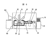
本発明の第2の実施例である微小試料加工観察装置の構成およびその動作を、装置全体
構成を示す図6,図7を用いて説明する。ここで、図7は図6の平面図を表しているが、
説明の都合上、機器の向きや詳細には幾分の相違があるが本質的差ではない。本装置では
、装置システムの中心部の真空試料室60の上部に、集束イオンビーム光学系31が垂直
に設置され、更に第2の集束イオンビーム光学系32が約40°傾斜して設置されている
。また、電子ビーム光学系41は約45°傾斜して設置されている。3基の光学系31,
32及び41は各々の中心軸がウェーハ21表面付近で一点に交わるように調整されてい
る。また、第1の実施例の装置と同様に、真空試料室60の内部には試料となるウェーハ
21を載置する試料台24が設置されている。ただし、本実施例の試料台24は水平移動
(X−Y),回転,上下移動する機能は有するが、傾斜機能は必ずしも必要ではない。
Further, in the EDX analysis in which the
(Example 2)
The configuration and operation of the micro sample processing and observation apparatus according to the second embodiment of the present invention will be described with reference to FIGS. Here, FIG. 7 shows a plan view of FIG.
For convenience of explanation, there are some differences in the orientation and details of the devices, but they are not essential. In this apparatus, a focused ion beam
32 and 41 are adjusted so that the respective central axes intersect at one point near the surface of the
次に、本装置による試料作製動作を、図4を用いて説明する。まず、集束イオンビーム
光学系31からFIB4をウェーハ21に照射して、図4に示すように観察分析位置p2
を横切ってコの字を描くように溝を形成する。ここまでは、実施の形態1と同様である。
次に、三角柱の斜面を形成するのは、もう一基の集束イオンビーム光学系32からのFIB4
により加工する。ただし、この状態では、微小試料22とウェーハ21とは支持部で接続
されている。この後、再び、集束イオンビーム光学系31からFIB4を用い、実施の形
態1と同様に微小試料を切取る。すなわち、微小試料22に、マニピュレータ70のプロ
ーブ保持部71先端のプローブ72を微小試料22の端部に接触させた後に、FIB4の
照射により堆積性ガスを接触点75に堆積させてプローブ72を微小試料22に接合し一
体化し、支持部をFIB4で切断して微小試料22を切取る。この後、微小試料22の観
察・分析等の工程は、実施の形態1と同様である。
Next, the sample preparation operation by this apparatus will be described with reference to FIG. First, the FIB 4 is irradiated onto the
A groove is formed so as to draw a U-shape across. The process up to this point is the same as in the first embodiment.
Next, the slope of the triangular prism is formed by the FIB4 from the other focused ion beam
To process. However, in this state, the
以上に述べたように、本実施の形態も、第1の実施例と同様に、高分解能で高速の観察
分析ができる。本実施の形態では、特に、2基の集束イオンビーム光学系を用いることに
より、試料台の傾斜を不要にできる。試料台の傾斜機構を省略できることにより試料台の
位置決め精度を数倍〜10倍以上向上できる。LSIデバイス製造現場では、近年各種ウ
ェーハ検査評価装置に異物検査や欠陥検査を行い、ウェーハ上の異常個所の特性並びに座
標データを収録し、その座標データをその後の更なる詳細検査用装置が受け取って指定座
標位置を割り出して観察分析を行うことが慣例になってきた。位置決め精度が高いことに
より試料ウェーハ21の観察個所の位置割り出し処理を自動化でき、しかもそのアルゴリ
ズムを単純化できる。これにより所要時間が大幅に短縮できるので高いスループットが得
られる。更には、傾斜機構を持たない試料台は小形軽量で高剛性を得やすく信頼性も増す
ので、より高品質な観察分析ができ、装置の小型化や低コスト化も可能になる。
As described above, this embodiment can perform high-resolution and high-speed observation analysis as in the first example. In the present embodiment, in particular, by using two focused ion beam optical systems, it is possible to eliminate the inclination of the sample stage. Since the tilt mechanism of the sample stage can be omitted, the positioning accuracy of the sample stage can be improved several times to 10 times or more. At the LSI device manufacturing site, in recent years, various types of wafer inspection / evaluation devices have been subjected to foreign matter inspection and defect inspection, and the characteristics and coordinate data of abnormal points on the wafer have been recorded. It has become customary to determine the designated coordinate position and perform observation analysis. Since the positioning accuracy is high, it is possible to automate the position indexing process of the observation location of the
尚、集束イオンビーム光学系31にスイング機能を待たせて垂直位置と傾斜位置の2ポ
ジションを適宜往来させることにより、試料台24を傾斜せずに、第2の実施例と同様の
処理が可能になり、本発明の効果を得ることができる。
(実施例3)
本発明の第3の実施例である微小試料加工観察装置の構成およびその動作を、装置全体
構成を示す図8,図9を用いて説明する。ここで、図9は図8の平面図を表しているが、
説明の都合上、機器の向きや詳細には幾分の相違があるが本質的差ではない。本実施例の
装置では、装置システムの中心部の真空試料室60の上部に、集束イオンビーム光学系
33が約45°傾斜して設置されている。また、電子ビーム光学系42も約45°傾斜し
て設置されている。2基の光学系33,42は各々の中心軸がウェーハ21表面付近で一
点に交わるように調整されている。また、第1の実施例の装置と同様に、真空試料室60
の内部には試料台24が設置されている。また第2の実施例と同様に、試料台24は傾斜
機能を持たない。
In addition, by making the focused ion beam
(Example 3)
The configuration and operation of a micro sample processing and observation apparatus according to a third embodiment of the present invention will be described with reference to FIGS. Here, FIG. 9 shows a plan view of FIG.
For convenience of explanation, there are some differences in the orientation and details of the devices, but they are not essential. In the apparatus of this embodiment, the focused ion beam
A
次に、本実施形態で、ウェーハ導入後の試料加工観察評価の過程を、図19を交えて説
明する。まず、試料台を下げてプローブ72の先端をウェーハ21から離した状態で、試
料台24に対して水平方向(XY方向)にプローブ72を移動し、プローブ72の先端を
FIB4の走査領域に設定する。マニピュレータ制御装置15は位置座標を保存した後、
プローブ72を退避する。
Next, in this embodiment, the process of sample processing observation evaluation after wafer introduction will be described with reference to FIG. First, in a state where the sample stage is lowered and the tip of the
The
集束イオンビーム光学系33の光軸を含む垂直平面とウェーハ上面の交線が、形成した
い試料の観察断面に重なる方向へ試料台の方角を合わせる。次にFIB4をウェーハ21
に照射し走査して観察に必要な長さと深さの垂直断面C1を形成する。次に、形成済みの
断面と交差する斜方切断面C2を形成する。この切断面C2の形成の際、斜面の傾斜角が
得られる位置まで試料台を水平に回転して方向を定める。次いで、垂直切断線に平行して
斜め溝をFIB4で形成する。更に、この溝に直角に一端C3を切断する。加工領域は、
長さ約5μm,幅約1μm,深さ約3μmであり、長さ約5μmの片持ち梁状態でウェー
ハ21と接続している。次に、微小試料22に、マニピュレータ70先端のプローブ72
を微小試料22の端部に接触させた後に、FIB4の照射により堆積性ガスを接触点75
に堆積させてプローブ72を微小試料22に接合し一体化する。その後、FIB4で微小
試料を支持する他端C4をFIB4で切断して微小試料22を切取る。微小試料22はプ
ローブ72に支持された状態になり、観察・分析を目的とする表面及び内部断面が微小試
料22の観察分析面p3として取り出す準備が完了する。以降の処理は、集束イオンビー
ム光学系による加工・観察、或いは電子ビーム光学系による観察に最適な方角へ微小試料
の向きを設定する際に試料台24の向きも適宜調整する必要が生じる以外は、第1の実施
例とほぼ同様につき説明を省く。
The direction of the sample stage is adjusted so that the line of intersection between the vertical plane including the optical axis of the focused ion beam
Is irradiated and scanned to form a vertical cross section C1 having a length and depth necessary for observation. Next, an oblique cut surface C2 intersecting with the formed cross section is formed. When the cut surface C2 is formed, the direction is determined by horizontally rotating the sample stage to a position where the slope angle can be obtained. Next, an oblique groove is formed by FIB 4 in parallel with the vertical cutting line. Further, one end C3 is cut at right angles to the groove. The processing area is
It has a length of about 5 μm, a width of about 1 μm, a depth of about 3 μm, and is connected to the
Is brought into contact with the end portion of the
The
以上に述べたように、本実施の形態も、第1の実施例と同様に、高分解能で高速の観察
分析ができる。本実施例は、1基の集束イオンビーム光学系を試料台に対して傾斜させる
ことにより、試料台に傾斜機能を持たせることなくウェーハから微小試料を切出して摘出
できる特長がある。光学系の周りには多くの機器を併せ搭載する必要があるのでスペース
難となっており、それらの機器の合計質量も大きいため取付基板の剛性確保を含めた設計
を難しいものにしている。またメンテナンス性も気掛かりとなる。本実施例は、試料台の
傾斜機構が不要で、しかも集束イオンビーム光学系が1基で済むため、構造が単純で軽量
小形にできコストも低減できる。
(実施例4)
本発明の第4の実施例である微小試料加工観察装置の概略構成を図10を用いて説明す
る。本実施例では、図3に示した微小試料加工観察装置の基本構成に、第2試料台18と
、第2試料台の角度や高さ等を制御する第2試料台制御装置19を加えたものである。本
実施例における集束イオンビーム光学系31からイオンビームを試料に照射してウェーハ
から微小試料を摘出するまでの過程は第1実施例と同様である。本実施例は、摘出した微
小試料を、マニピュレータで支持した状態で観察・分析する代わりに、第2試料台に固定
し観察・分析を行うものである。
As described above, this embodiment can perform high-resolution and high-speed observation analysis as in the first example. This embodiment has an advantage that a single sample ion beam optical system is tilted with respect to the sample stage, so that a minute sample can be cut out and extracted from the wafer without giving the tilt function to the sample stage. Since it is necessary to mount many devices around the optical system, space is difficult, and the total mass of these devices is large, which makes it difficult to design including securing the rigidity of the mounting board. Maintenance is also a concern. In this embodiment, the tilting mechanism of the sample stage is not required, and only one focused ion beam optical system is required. Therefore, the structure is simple, lightweight, and the cost can be reduced.
Example 4
A schematic configuration of a micro sample processing and observation apparatus according to a fourth embodiment of the present invention will be described with reference to FIG. In this embodiment, a
図11は、第2試料台18に微小試料22を固定した状態を示す。本実施例の第2試料
台18の微小試料固定部分には表面を平坦にした部材を用いているが、平坦であるかどう
かは問わない。微小試料の底面を第2試料台18に接触して、FIB4で堆積性ガスを第
2試料台18と微小試料22の接触点に堆積させて、アシストデポ膜76で第2試料台
18への微小試料22を固定する。なお、微小試料22作成時や、該堆積性ガスを堆積さ
せた時などに、観察断面の表面への異物吸着や観察断面の表面が破壊される不都合を予防
するために、FIB4の照射角を微小試料の観察断面に平行になるように第2試料台操作
で適切に角度設定した後、FIB4を照射して所望の観察断面を作成することもできる。
FIG. 11 shows a state in which the
図12に示す第2試料台を設置することにより複数の微小試料をまとめて扱うこともで
きる。ウェーハ21から微小試料22を摘出し、試料台脇の第2試料台18の適所へ固定
し、次の微小試料22を摘出する操作を繰り返すことにより、ウェーハ21を試料台24
に固定したまま複数個の断面観察と元素分析が可能であり、ウェーハ21全体に亘る断面
構造の分布を効率的に調べることができる。
By installing the second sample stage shown in FIG. 12, a plurality of minute samples can be handled together. By extracting the
A plurality of cross-sections can be observed and elemental analysis can be performed while being fixed to the wafer, and the distribution of the cross-sectional structure over the
図12において、第2試料台18に微小試料を数個並べて固定し、電子ビーム8に対し
て微小試料22が適切な角度になるように試料台24の停止方位と第2試料台18の角度
を併せ調整した状態で試料観察・分析を行えば、複数個の微小試料を連続的あるいは比較
しながら繰り返し観察分析できるので、ウェーハ21全体に亘って断面構造や元素分布を
詳細かつ能率的に調べることができる。また、図13に示す第2試料台18は、回転可能
な柱状の試料台の外周面に微小試料群を配列できるものであり、図12の場合より更に多
数の微小試料を一度に扱うことができる。
In FIG. 12, several micro samples are fixed side by side on the
また、微小試料22を試料回収トレイ内の指定位置に脱着して回収し、微小試料の識別
手段を付しておくことにより、事後の詳細評価が必要な場合に再び取りだし観察・分析を
実施することも可能である。
Further, the
以上に述べたように、本実施例も、ウェーハ表面を観察する場合と同程度の二次電子検
出効率が得られること、観察分析の角度を、垂直観察を含めた望ましい角度に調整できる
こと、真空雰囲気の試料室内に置いたまま観察できること、等により、微小試料22の観
察条件は非常に良好になるので、従来問題であった分解能の低下を回避でき、しかも最適
,綿密な観察分析を迅速で高効率に行うことができる。結果として高品質な観察分析を高
スループットで実行できる。
As described above, the secondary electron detection efficiency similar to that in the case of observing the wafer surface can be obtained in this embodiment, the angle of observation analysis can be adjusted to a desired angle including vertical observation, vacuum The observation condition of the
1…イオン源、2…レンズ、3…イオンビーム走査偏向器、4…集束イオンビーム
(FIB)、5…中央制御表示装置、6…二次電子検出器、7…電子銃、8…電子ビーム
、9…電子レンズ、10…電子ビーム走査偏向器、14…マニピュレータ、15…マニピ
ュレータ制御装置、16…X線検出器、17…堆積ガス供給装置、18…第2試料台、
19…第2試料台制御装置、21…ウェーハ、22…微小試料、23…カセット、24…
試料台、25…試料台制御装置、31…集束イオンビーム光学系、32…集束イオンビー
ム光学系、41…電子ビーム光学系、51…分析装置、60…真空試料室、61…ウェー
ハ搬送手段、62…ハッチ、63…載置台、70…マニピュレータ、71…プローブ保持
部、72…プローブ、75…アシストデポ膜、81…カセット導入手段、82…ウェーハ
搬送ロボット、83…オリエンテーション調整手段、90…ガス導入管、100…操作制
御部、101…試料、105…堆積性ガス、107…角穴、108…底穴、109…きり
かき溝、110…ガスノズル、p1…観察箇所、p2…観察分析面、p3…観察分析面、
s1…内部断面、s2…支持部。
DESCRIPTION OF
19 ... second sample stage control device, 21 ... wafer, 22 ... micro sample, 23 ... cassette, 24 ...
s1 ... internal cross section, s2 ... support part.
Claims (14)
前記試料から摘出された微小試料を支持できるマニピュレータと;
前記微小試料を固定できる第2試料台と;
前記試料台、及び前記第2試料台が配置された試料室と;
前記試料台に載置された前記試料、及び前記第2試料台に固定された前記微小試料にイオンビームを照射できる集束イオンビーム光学系と;
前記第2試料台に固定された前記微小試料に電子ビームを照射できる電子ビーム光学系と;
を備え、
前記第2試料台に固定された前記微小試料が、前記イオンビーム及び前記電子ビームに対して所定の角度となるよう、前記第2試料台の角度を制御できるように構成された微小試料加工観察装置。 A sample stage on which the sample is placed;
A manipulator capable of supporting a micro sample extracted from the sample;
A second sample stage capable of fixing the micro sample;
A sample chamber in which the sample stage and the second sample stage are arranged;
A focused ion beam optical system capable of irradiating an ion beam to the sample placed on the sample stage and the minute sample fixed to the second sample stage;
An electron beam optical system capable of irradiating the minute sample fixed to the second sample stage with an electron beam;
With
Microsample processing observation configured such that the angle of the second sample stage can be controlled so that the microsample fixed to the second sample stage has a predetermined angle with respect to the ion beam and the electron beam. apparatus.
前記試料から摘出された微小試料を支持できるマニピュレータと;
前記微小試料を固定できる第2試料台と;
前記試料台、及び前記第2試料台が配置された試料室と;
前記試料台に載置された前記試料、及び前記第2試料台に固定された前記微小試料にイオンビームを照射できる集束イオンビーム光学系と;
前記第2試料台に固定された前記微小試料に電子ビームを照射できる電子ビーム光学系と;
を備え、
前記第2試料台が、荷電粒子ビームの前記微小試料への照射角度可変機能を有することを特徴とする微小試料加工観察装置。 A sample stage on which the sample is placed;
A manipulator capable of supporting a micro sample extracted from the sample;
A second sample stage on which the micro sample can be fixed;
A sample chamber in which the sample stage and the second sample stage are arranged;
A focused ion beam optical system capable of irradiating an ion beam to the sample placed on the sample stage and the minute sample fixed to the second sample stage;
An electron beam optical system capable of irradiating the minute sample fixed to the second sample stage with an electron beam;
With
The second sample stage has a function of changing an irradiation angle of a charged particle beam to the minute sample.
前記試料から摘出された微小試料を支持できるマニピュレータと;
前記微小試料を固定できる第2試料台と;
前記試料台、及び前記第2試料台が配置された試料室と;
前記試料台に載置された前記試料、及び前記第2試料台に固定された前記微小試料にイオンビームを照射できる集束イオンビーム光学系と;
前記第2試料台に固定された前記微小試料に電子ビームを照射できる電子ビーム光学系と;
を備え、
前記電子ビームに対して前記微小試料が適切な角度となるように前記試料台の停止方位と前記第2試料台の角度を併せ調整するように構成された微小試料加工観察装置。 A sample stage on which the sample is placed;
A manipulator capable of supporting a micro sample extracted from the sample;
A second sample stage capable of fixing the micro sample;
A sample chamber in which the sample stage and the second sample stage are arranged;
A focused ion beam optical system capable of irradiating an ion beam to the sample placed on the sample stage and the minute sample fixed to the second sample stage;
An electron beam optical system capable of irradiating the minute sample fixed to the second sample stage with an electron beam;
With
An apparatus for processing and observing a micro sample configured to adjust both the stop direction of the sample stage and the angle of the second sample stage so that the micro sample has an appropriate angle with respect to the electron beam.
前記第2試料台を制御する第2試料台制御装置を含むことを特徴とする微小試料加工観察装置。 In the minute sample processing observation apparatus according to claim 1-3,
A micro sample processing / observation apparatus comprising a second sample stage control device for controlling the second sample stage.
前記試料から摘出された微小試料を支持できるマニピュレータと;
前記微小試料を固定できる第2試料台と;
前記試料台、及び前記第2試料台が配置された試料室と;
前記試料台に載置された前記試料、及び前記第2試料台に固定された前記微小試料にイオンビームを照射できる集束イオンビーム光学系と;
前記第2試料台に固定された前記微小試料に電子ビームを照射できる電子ビーム光学系と;
を備え、
前記イオンビーム及び前記電子ビームに対して前記微小試料が所定の角度となるように前記第2試料台を制御する第2試料台制御装置を備えた微小試料加工観察装置。 A sample stage on which the sample is placed;
A manipulator capable of supporting a micro sample extracted from the sample;
A second sample stage capable of fixing the micro sample;
A sample chamber in which the sample stage and the second sample stage are arranged;
A focused ion beam optical system capable of irradiating an ion beam to the sample placed on the sample stage and the minute sample fixed to the second sample stage;
An electron beam optical system capable of irradiating the minute sample fixed to the second sample stage with an electron beam;
With
A micro sample processing and observation apparatus comprising a second sample stage control device for controlling the second sample stage so that the micro sample is at a predetermined angle with respect to the ion beam and the electron beam.
前記試料から摘出された微小試料を支持できるマニピュレータと;
前記微小試料を固定できる第2試料台と;
前記試料台、及び前記第2試料台が配置された試料室と;
前記試料台に載置された前記試料、及び前記第2試料台に固定された前記微小試料にイオンビームを照射できる集束イオンビーム光学系と;
前記第2試料台に固定された前記微小試料に電子ビームを照射できる電子ビーム光学系と;
を備え、
前記第2試料台の角度や高さを制御する第2試料台制御装置を備えた微小試料加工観察装置。 A sample stage on which the sample is placed;
A manipulator capable of supporting a micro sample extracted from the sample;
A second sample stage capable of fixing the micro sample;
A sample chamber in which the sample stage and the second sample stage are arranged;
A focused ion beam optical system capable of irradiating an ion beam to the sample placed on the sample stage and the minute sample fixed to the second sample stage;
An electron beam optical system capable of irradiating the minute sample fixed to the second sample stage with an electron beam;
With
A micro sample processing and observation apparatus provided with a second sample stage control device for controlling the angle and height of the second sample stage.
前記マニピュレータが、前記微小試料を支持できるプローブを含むことを特徴とする微小試料加工観察装置。 In the micro sample processing observation device according to claim 1-6,
The micro sample processing observation apparatus, wherein the manipulator includes a probe capable of supporting the micro sample.
前記試料が電子デバイスであることを特徴とする微小試料加工観察装置。 In the micro sample processing observation device according to claim 1-6,
A micro sample processing observation apparatus, wherein the sample is an electronic device.
前記試料がマイクロデバイスであることを特徴とする微小試料加工観察装置。 In the micro sample processing observation device according to claim 1-6,
The sample processing observation apparatus, wherein the sample is a microdevice.
前記第2試料台が複数の前記微小試料を固定できることを特徴とする微小試料加工観察
装置。 In the minute sample processing observation apparatus according to claim 1-9 ,
An apparatus for processing and observing a micro sample, wherein the second sample stage can fix a plurality of the micro samples.
前記第2試料台が回転可能な柱状であることを特徴とする微小試料加工観察装置。 In the minute sample processing observation apparatus according to claim 1-10 ,
An apparatus for processing and observing a micro sample, wherein the second sample stage has a rotatable columnar shape.
前記微小試料の形状が5面体であることを特徴とする微小試料加工観察装置。 In the micro sample processing observation device according to claim 1-11 ,
An apparatus for processing and observing a minute sample, wherein the shape of the minute sample is a pentahedron.
前記微小試料の形状が4面体であることを特徴とする微小試料加工観察装置。 In the micro sample processing observation device according to claim 1-12 ,
An apparatus for processing and observing a minute sample, wherein the shape of the minute sample is a tetrahedron.
イオンビームの前記微小試料への照射角度を変更した後に、前記第2試料台に固定され
ている前記微小試料にイオンビームを照射することを特徴とする微小試料加工観察装置。
In the micro sample processing observation device according to claim 1-13 ,
An apparatus for processing and observing a micro sample, wherein the micro sample fixed to the second sample stage is irradiated with an ion beam after changing an irradiation angle of the ion beam to the micro sample.
Priority Applications (1)
| Application Number | Priority Date | Filing Date | Title |
|---|---|---|---|
| JP2005107006A JP3904018B2 (en) | 2005-04-04 | 2005-04-04 | Microsample processing observation method and apparatus |
Applications Claiming Priority (1)
| Application Number | Priority Date | Filing Date | Title |
|---|---|---|---|
| JP2005107006A JP3904018B2 (en) | 2005-04-04 | 2005-04-04 | Microsample processing observation method and apparatus |
Related Parent Applications (1)
| Application Number | Title | Priority Date | Filing Date |
|---|---|---|---|
| JP2004317452A Division JP4259454B2 (en) | 2004-11-01 | 2004-11-01 | Micro-sample processing observation equipment |
Publications (3)
| Publication Number | Publication Date |
|---|---|
| JP2005259706A JP2005259706A (en) | 2005-09-22 |
| JP2005259706A5 JP2005259706A5 (en) | 2006-03-09 |
| JP3904018B2 true JP3904018B2 (en) | 2007-04-11 |
Family
ID=35085183
Family Applications (1)
| Application Number | Title | Priority Date | Filing Date |
|---|---|---|---|
| JP2005107006A Expired - Lifetime JP3904018B2 (en) | 2005-04-04 | 2005-04-04 | Microsample processing observation method and apparatus |
Country Status (1)
| Country | Link |
|---|---|
| JP (1) | JP3904018B2 (en) |
Families Citing this family (1)
| Publication number | Priority date | Publication date | Assignee | Title |
|---|---|---|---|---|
| DE102020203580B4 (en) | 2020-03-20 | 2021-10-07 | Carl Zeiss Microscopy Gmbh | Method for changing the spatial orientation of a microsample in a microscope system, as well as computer program product |
-
2005
- 2005-04-04 JP JP2005107006A patent/JP3904018B2/en not_active Expired - Lifetime
Also Published As
| Publication number | Publication date |
|---|---|
| JP2005259706A (en) | 2005-09-22 |
Similar Documents
| Publication | Publication Date | Title |
|---|---|---|
| JP3736333B2 (en) | Micro sample processing observation equipment | |
| US7297965B2 (en) | Method and apparatus for sample formation and microanalysis in a vacuum chamber | |
| JP4259454B2 (en) | Micro-sample processing observation equipment | |
| JP5125123B2 (en) | Microsample processing observation method and apparatus | |
| JP3874011B2 (en) | Microsample processing observation method and apparatus | |
| JP4259604B2 (en) | Microsample processing observation method and apparatus | |
| JP2010232195A (en) | Method and device for observation of microsample processing | |
| JP3904019B2 (en) | Microsample processing observation method and apparatus | |
| JP3941816B2 (en) | Microsample processing observation method and apparatus | |
| JP4100450B2 (en) | Microsample processing observation method and apparatus | |
| JP4507952B2 (en) | Microsample processing observation method and apparatus | |
| JP5125174B2 (en) | Microsample processing observation method and apparatus | |
| JP3695181B2 (en) | Substrate extraction method and electronic component manufacturing method using the same | |
| JP3904018B2 (en) | Microsample processing observation method and apparatus | |
| JP4046144B2 (en) | Microsample processing observation method and apparatus | |
| JP3904020B2 (en) | Microsample processing observation method and apparatus | |
| JP4208031B2 (en) | Microsample processing observation method and apparatus | |
| JP5125184B2 (en) | Microsample processing observation method and apparatus | |
| JP5125143B2 (en) | Microsample processing observation method and apparatus | |
| JP5316626B2 (en) | Microsample processing observation method and apparatus | |
| JP5126031B2 (en) | Microsample processing observation method and apparatus | |
| JP4729390B2 (en) | Sample preparation equipment | |
| JP2004328003A (en) | Substrate extracting method and manufacturing method for electronic component using the same | |
| JPWO2006064548A1 (en) | Charged particle beam device and sample preparation method using the same | |
| JP4811448B2 (en) | Ion beam equipment |
Legal Events
| Date | Code | Title | Description |
|---|---|---|---|
| A521 | Request for written amendment filed |
Free format text: JAPANESE INTERMEDIATE CODE: A523 Effective date: 20060120 |
|
| A871 | Explanation of circumstances concerning accelerated examination |
Free format text: JAPANESE INTERMEDIATE CODE: A871 Effective date: 20060120 |
|
| A975 | Report on accelerated examination |
Free format text: JAPANESE INTERMEDIATE CODE: A971005 Effective date: 20060127 |
|
| A131 | Notification of reasons for refusal |
Free format text: JAPANESE INTERMEDIATE CODE: A131 Effective date: 20060307 |
|
| A521 | Request for written amendment filed |
Free format text: JAPANESE INTERMEDIATE CODE: A523 Effective date: 20060425 |
|
| RD01 | Notification of change of attorney |
Free format text: JAPANESE INTERMEDIATE CODE: A7421 Effective date: 20060425 |
|
| A131 | Notification of reasons for refusal |
Free format text: JAPANESE INTERMEDIATE CODE: A132 Effective date: 20061003 |
|
| A521 | Request for written amendment filed |
Free format text: JAPANESE INTERMEDIATE CODE: A523 Effective date: 20061030 |
|
| TRDD | Decision of grant or rejection written | ||
| A01 | Written decision to grant a patent or to grant a registration (utility model) |
Free format text: JAPANESE INTERMEDIATE CODE: A01 Effective date: 20061219 |
|
| A61 | First payment of annual fees (during grant procedure) |
Free format text: JAPANESE INTERMEDIATE CODE: A61 Effective date: 20070101 |
|
| R151 | Written notification of patent or utility model registration |
Ref document number: 3904018 Country of ref document: JP Free format text: JAPANESE INTERMEDIATE CODE: R151 |
|
| FPAY | Renewal fee payment (event date is renewal date of database) |
Free format text: PAYMENT UNTIL: 20100119 Year of fee payment: 3 |
|
| FPAY | Renewal fee payment (event date is renewal date of database) |
Free format text: PAYMENT UNTIL: 20110119 Year of fee payment: 4 |
|
| FPAY | Renewal fee payment (event date is renewal date of database) |
Free format text: PAYMENT UNTIL: 20110119 Year of fee payment: 4 |
|
| FPAY | Renewal fee payment (event date is renewal date of database) |
Free format text: PAYMENT UNTIL: 20120119 Year of fee payment: 5 |
|
| FPAY | Renewal fee payment (event date is renewal date of database) |
Free format text: PAYMENT UNTIL: 20130119 Year of fee payment: 6 |
|
| EXPY | Cancellation because of completion of term |